WO2024257633A1 - 半導体装置、電力変換装置、半導体装置の製造方法 - Google Patents
半導体装置、電力変換装置、半導体装置の製造方法 Download PDFInfo
- Publication number
- WO2024257633A1 WO2024257633A1 PCT/JP2024/020150 JP2024020150W WO2024257633A1 WO 2024257633 A1 WO2024257633 A1 WO 2024257633A1 JP 2024020150 W JP2024020150 W JP 2024020150W WO 2024257633 A1 WO2024257633 A1 WO 2024257633A1
- Authority
- WO
- WIPO (PCT)
- Prior art keywords
- semiconductor device
- semiconductor layer
- semiconductor
- region
- interface
- Prior art date
- Legal status (The legal status is an assumption and is not a legal conclusion. Google has not performed a legal analysis and makes no representation as to the accuracy of the status listed.)
- Ceased
Links
Images






Classifications
-
- H—ELECTRICITY
- H10—SEMICONDUCTOR DEVICES; ELECTRIC SOLID-STATE DEVICES NOT OTHERWISE PROVIDED FOR
- H10P—GENERIC PROCESSES OR APPARATUS FOR THE MANUFACTURE OR TREATMENT OF DEVICES COVERED BY CLASS H10
- H10P30/00—Ion implantation into wafers, substrates or parts of devices
- H10P30/20—Ion implantation into wafers, substrates or parts of devices into semiconductor materials, e.g. for doping
Definitions
- the technology disclosed in this specification relates to semiconductor technology.
- silicon carbide which has higher withstand voltages, lower resistance, and better heat resistance than silicon (Si) is being used in power semiconductor devices such as metal-oxide-semiconductor field-effect transistors (MOSFETs), insulated gate bipolar transistors (IGBTs), and Schottky barrier diodes (SBDs) (see, for example, Patent Document 1).
- MOSFETs metal-oxide-semiconductor field-effect transistors
- IGBTs insulated gate bipolar transistors
- SBDs Schottky barrier diodes
- SiC semiconductors have a high dielectric breakdown field, and the voltage-withstand layer (drift layer) required to achieve the same voltage can be made thinner compared to Si semiconductors, and furthermore, the impurity doping amount of the voltage-withstand layer can be increased.
- the interface between the SiC semiconductor substrate and the layer deposited on its top surface has the highest electric field.
- This interface has a discontinuous molecular structure, reflects the unevenness of the surface, and has many crystal defects, so when a high electric field is applied, leakage current occurs.
- junction barrier Schottky structure for passing current during reflux operation
- leakage current generates additional heat in the termination region, increasing thermal stress.
- the Schottky electrodes (barrier metal and source electrode) of the JBS formed in the termination region are prone to peeling.
- the technology disclosed in this specification was developed in consideration of the problems described above, and is a technology for preventing peeling of components that occurs when the temperature of a semiconductor device rises.
- the semiconductor device comprises an active region and a termination region surrounding the active region in a planar view, and in the termination region, comprises a first semiconductor layer of a first conductivity type, at least one second semiconductor layer of a second conductivity type provided on the surface layer of the first semiconductor layer, and a top electrode covering the first semiconductor layer and the second semiconductor layer, the top electrode being connected to the first semiconductor layer by a Schottky connection, and at least one interface between the second semiconductor layer and the top electrode being located deeper than the interface between the first semiconductor layer and the top electrode.
- the interface between the second semiconductor layer and the top electrode is located deeper than the interface between the first semiconductor layer and the top electrode, and adhesion is improved at that location through mechanical bonding, thereby making it possible to suppress peeling of the components due to thermal stress caused by a rise in temperature of the semiconductor device.
- 1 is a plan view of a semiconductor device according to an embodiment
- 2 is an enlarged view of the area indicated by the dashed line in FIG. 1, including the active region and the termination region; This is a cross-sectional view corresponding to the a-a' cross section in Figure 2.
- 4 is a flowchart showing an example of a manufacturing method of a semiconductor device according to the embodiment.
- 1A to 1C are cross-sectional views showing an example of a manufacturing method of a semiconductor device in an embodiment.
- 1A to 1C are cross-sectional views showing an example of a manufacturing method of a semiconductor device in an embodiment.
- 1A to 1C are cross-sectional views showing an example of a manufacturing method of a semiconductor device in an embodiment.
- 1A to 1C are cross-sectional views showing an example of a manufacturing method of a semiconductor device in an embodiment.
- 2 is a cross-sectional view of a termination region of a semiconductor device according to an embodiment;
- 2 is a cross-sectional view of a termination region of a semiconductor device according to an embodiment;
- 1 is a plan view of a semiconductor device according to an embodiment;
- 18 is an enlarged view of the area indicated by the dashed dotted line in FIG. 17, including the active region and the termination region.
- 1 is a diagram conceptually illustrating an example of a configuration of a power conversion system including a power conversion device according to an embodiment.
- the upper surface of " or “the lower surface of " when it is stated that “the upper surface of " or “the lower surface of " is used, it is intended to include not only the upper surface or lower surface of the target component itself, but also a state in which another component is formed on the upper surface or lower surface of the target component.
- the upper surface of " or “the lower surface of " when it is stated that "B is provided on the upper surface of A,” it does not prevent another component "C" from being interposed between A and B.
- a power semiconductor device which is a MOSFET made of an n-channel SiC substrate.
- the semiconductor device is a planar gate type semiconductor device and includes a built-in Schottky barrier diode (SBD).
- FIG. 1 is a plan view of a semiconductor device according to this embodiment.
- a source electrode 3 is formed in the center of the top surface of the semiconductor device 1, and a gate wiring 2 is formed to surround the source electrode 3.
- a gate pad 4 is formed in the lower center and is electrically connected to the gate wiring 2.
- the region in which the unit cells are periodically arranged is defined as the active region, and the region other than the active region (the region surrounding the active region) is defined as the termination region.
- FIG. 2 is an enlarged view of the region including the active region and termination region indicated by the dashed line in FIG. 1.
- unit cells 14 (corresponding to the MOSFET region) are formed in a stripe pattern in active region 13, which is made up of a MOSFET region in which a MOSFET structure is formed and an SBD region in which an SBD structure is formed.
- FIG. 3 is a cross-sectional view corresponding to the a-a' cross section in FIG. 2.
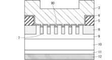
- the termination region of the semiconductor device includes an n-type SiC substrate 11, an n-type epitaxial growth layer 10 uniformly formed on the upper surface of the SiC substrate 11, an n-type n-well region 9 formed on the surface of the epitaxial growth layer 10, a p-type semiconductor region 7 partially formed on the surface of the n-well region 9, a p-type p-well region 8 partially formed on the surface of the n-well region 9, an interlayer insulating film 5 formed to cover a part of the upper surface of the p-well region 8, a barrier metal layer 6 formed to cover the interlayer insulating film 5, the n-well region 9, the p-type semiconductor region 7, and the p-well region 8, a source electrode 3 formed to cover the barrier metal layer 6, and a drain electrode 12 formed on the lower surface of the n-type SiC substrate 11.
- the interface between the p-type semiconductor region 7 and the barrier metal layer 6 is formed at a deeper position than the interface between the n-well region 9 and the barrier metal layer 6.
- the interface between the barrier metal layer 6 and the p-type semiconductor region 7, and part of the interface between the barrier metal layer 6 and the p-well region 8, are ohmic-connected.
- the interface between the barrier metal layer 6 and the n-well region 9 is Schottky-connected (i.e., the source electrode 3 and the n-well region 9 are Schottky-connected).
- the interface between the p-type semiconductor region 7 and the source electrode 3 (in FIG. 3, the interface between the p-type semiconductor region 7 and the barrier metal layer 6) is formed so as to satisfy D1>0, D2>0, and (D2 ⁇ 2)>D1.
- FIG. 4 is a flow chart showing an example of a method for manufacturing a semiconductor device according to the present embodiment.
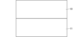
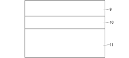
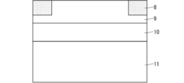
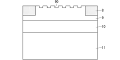
- Fig. 5 to Fig. 14 are cross-sectional views showing an example of a method for manufacturing a semiconductor device according to the present embodiment.
- an epitaxial growth layer 10 made of n-type SiC is formed on the top surface (first main surface) of an n-type SiC substrate 11 having a polytype of 4H, for example, by chemical vapor deposition (CVD) (step ST1 in FIG. 4).
- CVD chemical vapor deposition
- impurities are ion-implanted into the surface layer of the epitaxial growth layer 10 to form an n-well region 9 (step ST2 in FIG. 4).
- the impurity concentration of the n-well region 9 is controlled to be higher than the impurity concentration of the epitaxial growth layer 10.
- an implantation mask is formed in a portion of the n-well region 9 using photoresist or the like (not shown here), and then p-type impurities are ion-implanted from the top surface of the n-well region 9 to form the p-well region 8 (step ST3 in FIG. 4).
- p-type impurities include B (boron) and Al (aluminum).
- the implantation depth of the p-well region 8 is controlled so as not to deviate from the n-well region 9 (i.e., so that the implantation depth of the p-well region 8 is not deeper than the bottom surface of the n-well region 9).
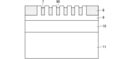
- an implantation mask is formed (not shown) using photoresist or the like in a portion of the n-well region 9 (in FIG. 8, the region where the p-well region 8 is not formed), and then a portion of the upper surface of the n-well region 9 is processed using dry etching or wet etching technology to form a recess 90 (step ST4 in FIG. 4).
- p-type impurities are ion-implanted into the recess 90 to form the p-type semiconductor region 7 (step ST5 in FIG. 4).
- the impurity concentration of the p-type semiconductor region 7 is controlled to be higher than the impurity concentration of the p-well region 8.
- the SiC substrate 11 is heat-treated at high temperature using a heat treatment device (not shown), and the implanted ions are electrically activated.
- an interlayer insulating film 5 is formed by a deposition method such as thermal oxidation or chemical vapor deposition, and then patterned using photolithography, dry etching, or wet etching so that the interlayer insulating film 5 remains in a predetermined area (step ST6 in FIG. 4).
- the interlayer insulating film may have a laminated structure of two or more layers of different materials.
- a barrier metal layer 6 is formed using a barrier metal made of titanium or a titanium compound such as titanium nitride (TiN).
- a film of aluminum, an aluminum alloy made of aluminum and silicon, or nickel is deposited to form the source electrode 3 (step ST7 in FIG. 4).
- a nickel film of about 600 nm is formed on the lower surface (second main surface) of the SiC substrate 11 by appropriately using a sputtering method or the like to form the drain electrode 12 (step ST9 in FIG. 4).
- the drain electrode 12 may be a laminated film made of a nickel film and gold or silver, etc., with a metal that is poorly reactive with the outside, such as gold (Au) or silver (Ag), used as a protective film on the nickel surface.
- This stress can cause the barrier metal layer 6 to peel off from the SiC substrate 11, or the source electrode 3 to peel off from the barrier metal layer 6.
- the amount of heat generated in the termination region increases compared to a semiconductor device without an SBD region. Therefore, when the barrier metal layer 6 and the source electrode 3 are formed on the top surface of the flat SiC substrate 11, there is a problem that the barrier metal layer 6 or the source electrode 3 peels off due to thermal stress caused by a rise in temperature when current is applied to the semiconductor device, as they have poor adhesion to lateral stress.
- the interface can be mechanically bonded (also called the anchor effect, fastener effect, or anchor effect) to increase adhesion and suppress peeling. This improves the reliability of the semiconductor device during operation.
- the p-type semiconductor region 7 by forming the p-type semiconductor region 7 by ion implanting p-type impurities into the recesses 90 of the n-well region 9, the p-type semiconductor region 7 can be formed to the same depth with lower acceleration energy compared to a structure in which ions are implanted without forming an uneven surface at the interface, and energy costs during manufacturing can be reduced. Furthermore, lowering the injection energy can reduce damage caused by ion implantation on the top surface of the SiC substrate 11, and suppress leakage current due to defects that may be formed due to the damage. This suppresses heat generation during operation of the semiconductor device 1, improving the reliability of the semiconductor device 1.
- Second Embodiment A semiconductor device and a method for manufacturing the semiconductor device according to the present embodiment will be described.
- components similar to those described in the above embodiment are illustrated with the same reference numerals, and detailed description thereof will be omitted as appropriate.
- the power semiconductor device according to the first embodiment is applied to a power conversion device.
- a power semiconductor device will be described using an n-channel MOSFET made of a SiC substrate.
- This semiconductor device is a planar gate type semiconductor device and has a built-in Schottky barrier diode (SBD).
- SBD Schottky barrier diode
- Figure 15 is a cross-sectional view of the termination region of the semiconductor device according to this embodiment.
- the device includes an n-type SiC substrate 11, an n-type epitaxial growth layer 10, an n-type n-well region 9, a plurality of p-type semiconductor regions 7a partially formed on the surface layer of the n-well region 9, a p-type p-well region 8, an interlayer insulating film 5, a barrier metal layer 6, a source electrode 3, and a drain electrode 12.
- a recess 90 is formed in the upper surface of the n-well region 9, as in the first embodiment.
- the p-type semiconductor region 7a is formed with a width that covers the recess 90 in a plan view (a range wider than the range in which the recess 90 is formed).
- the manufacturing method of the semiconductor device according to this embodiment differs in that, when ion-implanting p-type impurities to form p-type semiconductor region 7a, ion implantation is performed from a direction at an angle of 1° or more and 45° or less from a direction perpendicular to SiC substrate 11.
- the other manufacturing steps are the same as those shown in FIGS.
- the power semiconductor device according to the first or second embodiment is applied to a power conversion device.
- a power semiconductor device will be described, taking as an example a MOSFET made of an n-channel SiC substrate.
- This semiconductor device is a planar gate type semiconductor device, and includes a built-in Schottky barrier diode (SBD).
- SBD Schottky barrier diode
- Figure 16 is a cross-sectional view of the termination region of the semiconductor device according to this embodiment.
- the device includes an n-type SiC substrate 11, an n-type epitaxial growth layer 10, an n-type n-well region 9, a p-type semiconductor region 7, a p-type p-well region 8, an interlayer insulating film 5, a barrier metal layer 6b formed to cover the interlayer insulating film 5, the n-well region 9, the p-type semiconductor region 7, and the p-well region 8, a source electrode 3, and a drain electrode 12.
- a recess 90b is formed on the top surface of the n-well region 9.
- the interior angle of the bottom of the recess 90b is an obtuse angle of 90° or more.
- the barrier metal layer 6b is formed with an inclined surface so as to follow the shape of the recess 90b.
- the p-type semiconductor region provided below the recess 90b may be formed in an area larger than the area in which the recess 90b is formed.
- the manufacturing method of the semiconductor device according to this embodiment differs from the process of the first embodiment shown in Fig. 8 in that when forming the recess 90b, the side surface of the recess 90b is formed to be an inclined surface by wet etching or the like.
- the other manufacturing steps are the same as those shown in Figs. 5 to 14.
- a SiC semiconductor device that can suppress damage or peeling at the corners of the end of the recess 90 in a planar view by alleviating the concentration of electric field and stress at the corners of the end of the recess 90 in a planar view.
- FIG. 17 is an enlarged view of a region including the active region and the termination region of the above-mentioned SiC semiconductor device.
- FIG. 18 is an enlarged view of a region including a recess 90, which is indicated by a dashed line in FIG. 17.
- the concentration of electric fields and stresses at the corners of the end of the recess 90 in a planar view can be alleviated, thereby suppressing damage or peeling at the corners of the end of the recess 90 in a planar view.
- the mask for forming the recess 90 in step ST4 is changed. Then, through steps similar to steps ST5 to ST9 in the first embodiment, a SiC semiconductor device having a structure as shown in FIGS. 17 and 18 is formed.
- the semiconductor device according to the above-described embodiment is applied to a power converter.
- the power converter to which the semiconductor device is applied is not limited to a specific application, but the following describes a case where the semiconductor device is applied to a three-phase inverter.
- FIG. 19 is a conceptual diagram illustrating an example of the configuration of a power conversion system including the power conversion device of this embodiment.
- the power conversion device 2200 is a three-phase inverter connected between the power source 2100 and the load 2300.
- the power conversion device 2200 converts the DC power supplied from the power source 2100 into AC power, and further supplies the AC power to the load 2300.
- the power conversion device 2200 includes a conversion circuit 2201 that converts DC power into AC power and outputs it, a drive circuit 2202 that outputs drive signals for driving each switching element of the conversion circuit 2201, and a control circuit 2203 that outputs a control signal to the drive circuit 2202 to control the drive circuit 2202.
- the conversion circuit 2201 in this embodiment is a two-level three-phase full bridge circuit, and has six switching elements and six freewheeling diodes connected in anti-parallel to each switching element.
- a semiconductor device is applied to at least one of the switching elements and free wheel diodes in the conversion circuit 2201.
- the six switching elements are connected in series in groups of two to form upper and lower arms, and each upper and lower arm forms one phase of the full bridge circuit (i.e., U phase, V phase, and W phase).
- the output terminals of each upper and lower arm i.e., the three output terminals of the conversion circuit 2201 are connected to the load 2300.
- the drive circuit 2202 generates a drive signal for driving the switching element of the conversion circuit 2201, and further supplies the drive signal to the control electrode of the switching element of the conversion circuit 2201. Specifically, based on a control signal output from the control circuit 2203 described below, the drive circuit 2202 outputs a drive signal for turning the switching element on and a drive signal for turning the switching element off to the control electrodes of the respective switching elements.
- the drive signal When the switching element is maintained in the on state, the drive signal is a voltage signal equal to or greater than the threshold voltage of the switching element (i.e., an on signal), and when the switching element is maintained in the off state, the drive signal is a voltage signal equal to or less than the threshold voltage of the switching element (i.e., an off signal).
- the semiconductor device in any of the embodiments described above may be applied to a three-level or multi-level power conversion device.
- the semiconductor device in any of the embodiments described above may be applied to a single-phase inverter.
- the semiconductor device when supplying power to a DC load, can be applied to a DC-DC converter or an AC-DC converter.
- a power conversion device to which a semiconductor device according to any of the above-described embodiments is applied is not limited to cases in which the load described above is an electric motor, and can also be used, for example, as a power supply device for an electric discharge machine, a laser processing machine, an induction heating cooker, or a non-contact power supply system.Furthermore, a power conversion device to which a semiconductor device according to any of the above-described embodiments is applied can also be used as a power conditioner in a solar power generation system or a power storage system, etc.
- a semiconductor device is manufactured using the manufacturing method described in the embodiment described above. Then, a conversion circuit 2201 having the semiconductor device is provided as a component of a power conversion device.
- the conversion circuit 2201 is a circuit for converting input power and outputting it.
- a drive circuit 2202 is provided as a component of the power conversion device.
- the drive circuit 2202 is a circuit for outputting a drive signal to the semiconductor device for driving the semiconductor device.
- the power conversion device is further provided with a control circuit 2203.
- the control circuit 2203 is a circuit for outputting a control signal to the drive circuit 2202 for controlling the drive circuit 2202.
- the semiconductor switching elements used in the embodiments described above are not limited to switching elements made of silicon (Si) semiconductors, and may be made of, for example, non-Si semiconductor materials that have a wider band gap than Si semiconductors.
- Wide band gap semiconductors that are non-Si semiconductor materials include, for example, silicon carbide, gallium nitride-based materials, and diamond.
- Switching elements made of wide bandgap semiconductors can be used in high voltage regions where unipolar operation is difficult with silicon semiconductors, and can significantly reduce the switching losses that occur during switching operations. This allows for a significant reduction in power loss.
- switching elements made of wide band gap semiconductors have low power loss and high heat resistance. Therefore, when configuring a power module with a cooling section, it is possible to reduce the size of the heat dissipation fins of the heat sink, making it possible to further reduce the size of the semiconductor module.
- switching elements made of wide bandgap semiconductors are suitable for high-frequency switching operations. Therefore, when applied to converter circuits that require high frequencies, increasing the switching frequency can also reduce the size of reactors or capacitors connected to the converter circuit.
- the semiconductor switching element in the above-described embodiment is a switching element made of a wide-gap semiconductor such as silicon carbide.
- the semiconductor device includes an active region 13 and a termination region surrounding the active region 13 in a planar view.
- the termination region includes a first semiconductor layer of a first conductivity type (n-type), a second semiconductor layer of a second conductivity type (p-type), and a top electrode.
- the first semiconductor layer corresponds to, for example, the n-well region 9.
- the second semiconductor layer corresponds to, for example, at least one of the p-type semiconductor region 7, the p-type semiconductor region 7a, and the p-well region 8.
- the top electrode corresponds to, for example, the source electrode 3. At least one p-type semiconductor region 7 is provided on the surface layer of the n-well region 9.
- the source electrode 3 covers the n-well region 9 and the p-type semiconductor region 7.
- the source electrode 3 is connected to the n-well region 9 via a Schottky connection.
- at least one interface between the p-type semiconductor region 7 and the source electrode 3 (if a barrier metal layer 6 is present, the interface between the barrier metal layer 6 and the p-type semiconductor region 7) is located deeper than the interface between the n-well region 9 and the source electrode 3 (if a barrier metal layer 6 is present, the interface between the barrier metal layer 6 and the n-well region 9).
- the interface between the p-type semiconductor region 7 and the source electrode 3 is located deeper than the interface between the n-well region 9 and the source electrode 3, and the mechanical bond at this location improves adhesion, making it possible to suppress peeling of the source electrode 3 from the barrier metal layer 6 or the n-well region 9 due to thermal stress caused by a rise in temperature of the semiconductor device. This improves the reliability of the semiconductor device during operation.
- the distance from the interface between the n-well region 9 and the source electrode 3 (if a barrier metal layer 6 is present, the interface between the barrier metal layer 6 and the n-well region 9) to the interface between the p-type semiconductor region 7 and the source electrode 3 (if a barrier metal layer 6 is present, the interface between the barrier metal layer 6 and the p-type semiconductor region 7) is D1
- the distance from the interface between the n-well region 9 and the source electrode 3 (if a barrier metal layer 6 is present, the interface between the barrier metal layer 6 and the n-well region 9) to the underside of the p-type semiconductor region 7 is D2
- the interface between the p-type semiconductor region 7 and the source electrode 3 (if a barrier metal layer 6 is present, the interface between the barrier metal layer 6 and the p-type semiconductor region 7) is formed so as to satisfy D1>0, D2>0, and (D2 ⁇ 2)>D1.
- This configuration makes it possible to suppress peeling between the source electrode 3 and the n-well region 9 (or between the source electrode 3 and the barrier metal layer 6, or between the barrier metal layer 6 and the n-well region 9, if a barrier metal layer 6 is used) due to thermal stress that occurs during operation of the semiconductor device, without impairing the characteristics of the JBS.
- the active region 13 has a Schottky barrier diode structure.
- the active region 13 has a MOSFET structure.
- the region having the MOSFET structure and the region having the Schottky barrier diode structure are periodically arranged in a striped pattern in a plan view.
- a recess 90 (or recess 90b) is formed on the upper surface of the n-well region 9.
- the p-type semiconductor region 7a is provided to cover an area larger than the area in which the recess 90 (or recess 90b) is formed.
- the side surface of the recess 90b is an inclined surface.
- the power conversion device has the above-mentioned semiconductor device, and is equipped with a conversion circuit 2201 that converts and outputs input power, a drive circuit 2202 that outputs a drive signal to the semiconductor device for driving the semiconductor device, and a control circuit 2203 that outputs a control signal to the drive circuit 2202 for controlling the drive circuit 2202.
- the interface between the p-type semiconductor region 7 and the source electrode 3 is located deeper than the interface between the n-well region 9 and the source electrode 3, and the adhesion is improved by mechanical bonding at that location, so that peeling of the source electrode 3 from the barrier metal layer 6 or the n-well region 9 can be suppressed due to thermal stress caused by a temperature rise in the semiconductor device. This can improve the reliability of the semiconductor device during operation.
- At least one p-type semiconductor region 7 of a second conductivity type is provided on the surface of an n-well region 9 of a first conductivity type in the termination region.
- a source electrode 3 is provided in the termination region to cover the n-well region 9 and the p-type semiconductor region 7.
- the source electrode 3 is connected to the n-well region 9 by a Schottky connection.
- at least one interface between the p-type semiconductor region 7 and the source electrode 3 is located deeper than the interface between the n-well region 9 and the source electrode 3.
- the interface between the p-type semiconductor region 7 and the source electrode 3 is located deeper than the interface between the n-well region 9 and the source electrode 3, and the mechanical bond at this location improves adhesion, making it possible to suppress peeling of the source electrode 3 from the barrier metal layer 6 or the n-well region 9 due to thermal stress caused by a rise in temperature of the semiconductor device. This improves the reliability of the semiconductor device during operation.
- a conversion circuit 2201 that has a semiconductor device manufactured by the above manufacturing method and converts and outputs input power.
- a drive circuit 2202 is provided that outputs a drive signal to the semiconductor device for driving the semiconductor device.
- a control circuit 2203 is provided that outputs a control signal to the drive circuit 2202 for controlling the drive circuit 2202.
- the interface between the p-type semiconductor region 7 and the source electrode 3 is located deeper than the interface between the n-well region 9 and the source electrode 3, and the adhesion is improved by mechanical bonding at that location, so that peeling of the source electrode 3 from the barrier metal layer 6 or the n-well region 9 can be suppressed due to thermal stress caused by a rise in temperature of the semiconductor device. This can improve the reliability of the semiconductor device during operation.
- each component in the embodiments described above is a conceptual unit, and the scope of the technology disclosed in this specification includes cases where one component is made up of multiple structures, where one component corresponds to a part of a structure, and even where multiple components are provided in one structure.
- each component in the embodiments described above includes structures having other structures or shapes as long as they perform the same function.
- (Appendix 1) an active region and a termination region surrounding the active region in a plan view; In the termination region, a first semiconductor layer of a first conductivity type; At least one second semiconductor layer of a second conductivity type is provided on a surface layer of the first semiconductor layer; a top electrode covering the first semiconductor layer and the second semiconductor layer; the upper electrode is in Schottky contact with the first semiconductor layer; At least one interface between the second semiconductor layer and the top electrode is located deeper than an interface between the first semiconductor layer and the top electrode.
- Semiconductor device In the termination region, a first semiconductor layer of a first conductivity type; At least one second semiconductor layer of a second conductivity type is provided on a surface layer of the first semiconductor layer; a top electrode covering the first semiconductor layer and the second semiconductor layer; the upper electrode is in Schottky contact with the first semiconductor layer; At least one interface between the second semiconductor layer and the top electrode is located deeper than an interface between the first semiconductor layer and the top electrode.
- (Appendix 2) 2. The semiconductor device according to claim 1, a distance from an interface between the first semiconductor layer and the upper electrode to an interface between the second semiconductor layer and the upper electrode is defined as D1; When the distance from the interface between the first semiconductor layer and the upper electrode to the lower surface of the second semiconductor layer is D2, The interface between the second semiconductor layer and the upper electrode is formed so as to satisfy D1>0, D2>0, and (D2 ⁇ 2)>D1. Semiconductor device.
- the semiconductor device according to claim 1 The active region has a Schottky barrier diode structure.
- the semiconductor device according to claim 3 has a MOSFET structure, a region having a MOSFET structure and a region having a Schottky barrier diode structure are periodically arranged in a striped pattern in a plan view; Semiconductor device.
- a semiconductor device according to any one of claims 1 to 4, A recess is formed on an upper surface of the first semiconductor layer, The second semiconductor layer is provided to cover an area larger than an area in which the recess is formed. Semiconductor device.
- At least one corner of the end of the second semiconductor layer in a plan view is an obtuse angle or a curved surface.
- a conversion circuit including the semiconductor device according to any one of claims 1 to 7 and configured to convert and output an input power; a drive circuit that outputs a drive signal for driving the semiconductor device to the semiconductor device; a control circuit that outputs a control signal to the drive circuit for controlling the drive circuit; Power conversion equipment.
- a method for manufacturing a semiconductor device including an active region and a termination region surrounding the active region in a plan view, In the termination region, At least one second semiconductor layer of a second conductivity type is provided on a surface layer of a first semiconductor layer of a first conductivity type; providing a top electrode covering the first semiconductor layer and the second semiconductor layer; the upper electrode is in Schottky contact with the first semiconductor layer; At least one interface between the second semiconductor layer and the top electrode is located deeper than an interface between the first semiconductor layer and the top electrode.
- 1 semiconductor device 2 gate wiring, 3 source electrode, 4 gate pad, 5 interlayer insulating film, 6 barrier metal layer, 6b barrier metal layer, 7 p-type semiconductor region, 7a p-type semiconductor region, 8 p-well region, 9 n-well region, 10 epitaxial growth layer, 11 SiC substrate, 12 drain electrode, 13 active region, 14 unit cell, 90 recess, 90b recess, 2100 power supply, 2200 power conversion device, 2201 conversion circuit, 2202 drive circuit, 2203 control circuit, 2300 load.
Landscapes
- Electrodes Of Semiconductors (AREA)
Abstract
半導体装置の温度上昇に伴う部材の剥離を抑制する。半導体装置は、活性領域と、活性領域を平面視で囲む終端領域とを備え、終端領域において、第1の導電型の第1の半導体層と、第1の半導体層の表層に少なくとも1つ設けられる、第2の導電型の第2の半導体層と、第1の半導体層および第2の半導体層を覆う上面電極とを備え、上面電極が第1の半導体層とショットキー接続し、少なくとも1つの、第2の半導体層と上面電極との界面が、第1の半導体層と上面電極との界面よりも深く位置する。
Description
本願明細書に開示される技術は、半導体技術に関するものである。
半導体装置の高耐圧化、低損失化、高温環境下での使用などを可能とするため、シリコン(Si)に比べて、高耐電圧、低抵抗で耐熱性に優れる、炭化珪素(SiC)を用いて、金属-酸化膜-半導体電界効果トランジスタ(metal-oxide-semiconductor field-effect transistor、すなわち、MOSFET)、絶縁ゲート型バイポーラトランジスタ(insulated gate bipolar transistor、すなわち、IGBT)、または、ショットキーバリアダイオード(Schottky barrier diode、すなわち、SBD)などの電力用半導体装置への応用がなされている(たとえば、特許文献1を参照)。
耐圧が、たとえば、1kV以上、かつ、1.2kV以下程度のSiC半導体MOSFETの場合、2mΩcm2以下のオン抵抗が得られており、同耐圧のSi半導体MOSFETまたはIGBTと比較すると、その抵抗値は半分以下である。
SiC半導体を用いることで、オン抵抗をSi半導体に比べて大幅に低減することができる理由は、SiC半導体が高い絶縁破壊電界を有し、同耐圧を実現するための耐圧層(ドリフト層)をSi半導体に比べて薄くすることができること、さらに、耐圧層の不純物ドーピング量を高くすることができること、などである。
今後、半導体装置に通電する電流密度を上げることで搭載する半導体装置を小型化したり、MOSFETの中に寄生するダイオードを用いることで搭載する半導体装置の数を減らしたりすることで、半導体装置の製造コストを低減することができるため、インバータ部品としてSi半導体製IGBTの大半がSiC半導体製のものに置き換えられていくと考えられる。
半導体装置に通電する際の終端領域において、SiC半導体基板とその上面に堆積している層との境界面が最も高い電界となる。この境界面は分子構造が不連続であったり、表面の凹凸形状が反映されていたり、結晶欠陥などが多く存在したりして、高い電界が印加されるとリーク電流が発生する。
特に還流動作時の電流を流すための領域(ジャンクション・バリア・ショットキー構造、すなわち、JBS)が形成された半導体装置においては、リーク電流によって終端領域でさらに発熱が生じて熱応力が大きくなる。そのため、終端領域に形成されるJBSのショットキー電極(バリアメタルおよびソース電極)が剥離しやすくなるという課題がある。
本願明細書に開示される技術は、以上に記載されたような問題を鑑みてなされたものであり、半導体装置の温度上昇に伴う部材の剥離を抑制するための技術である。
本願明細書に開示される技術の第1の態様である半導体装置は、活性領域と、前記活性領域を平面視で囲む終端領域とを備え、前記終端領域において、第1の導電型の第1の半導体層と、前記第1の半導体層の表層に少なくとも1つ設けられる、第2の導電型の第2の半導体層と、前記第1の半導体層および前記第2の半導体層を覆う上面電極とを備え、前記上面電極が前記第1の半導体層とショットキー接続し、少なくとも1つの、前記第2の半導体層と前記上面電極との界面が、前記第1の半導体層と前記上面電極との界面よりも深く位置する。
本願明細書に開示される技術の少なくとも第1の態様によれば、第2の半導体層と上面電極との界面が、第1の半導体層と上面電極との界面よりも深く位置して当該箇所で機械的結合によって密着性を向上させることによって、半導体装置の温度上昇で生じる熱応力に対して部材の剥離を抑制することができる。
また、本願明細書に開示される技術に関連する目的と、特徴と、局面と、利点とは、以下に示される詳細な説明と添付図面とによって、さらに明白となる。
以下、添付される図面を参照しながら実施の形態について説明する。以下の実施の形態では、技術の説明のために詳細な特徴なども示されるが、それらは例示であり、実施の形態が実施可能となるために、それらのすべてが必ずしも必須の特徴ではない。
なお、図面は概略的に示されるものであり、説明の便宜のため、適宜、構成の省略、または、構成の簡略化などが図面においてなされる。また、異なる図面にそれぞれ示される構成などの大きさおよび位置の相互関係は、必ずしも正確に記載されるものではなく、適宜変更され得るものである。また、断面図ではない平面図などの図面においても、実施の形態の内容を理解することを容易にするために、ハッチングが付される場合がある。
また、以下に示される説明では、同様の構成要素には同じ符号を付して図示し、それらの名称と機能とについても同様のものとする。したがって、それらについての詳細な説明を、重複を避けるために省略する場合がある。
また、本願明細書に記載される説明において、ある構成要素を「備える」、「含む」または「有する」などと記載される場合、特に断らない限りは、他の構成要素の存在を除外する排他的な表現ではない。
また、本願明細書に記載される説明において、「第1の」または「第2の」などの序数が使われる場合があっても、これらの用語は、実施の形態の内容を理解することを容易にするために便宜上使われるものであり、実施の形態の内容はこれらの序数によって生じ得る順序などに限定されるものではない。
また、本願明細書に記載される説明において、「上」、「下」、「左」、「右」、「側」、「底」、「表」または「裏」などの特定の位置または方向を意味する用語が使われる場合があっても、これらの用語は、実施の形態の内容を理解することを容易にするために便宜上使われるものであり、実施の形態が実際に実施される際の位置または方向とは関係しないものである。
また、本願明細書に記載される説明において、「…の上面」または「…の下面」などと記載される場合、対象となる構成要素の上面自体または下面自体に加えて、対象となる構成要素の上面または下面に他の構成要素が形成された状態も含むものとする。すなわち、たとえば、「Aの上面に設けられるB」と記載される場合、AとBとの間に別の構成要素「C」が介在することを妨げるものではない。
<第1の実施の形態>
以下、本実施の形態に関する半導体装置、および、半導体装置の製造方法について説明する。
以下、本実施の形態に関する半導体装置、および、半導体装置の製造方法について説明する。
<半導体装置の構成について>
本実施の形態に関する半導体装置として、電力用半導体装置であって、nチャネル型のSiC基板からなるMOSFETを例にとって説明する。当該半導体装置は、プレーナゲート型の半導体装置であり、ショットキーバリアダイオード(SBD)を内蔵している。
本実施の形態に関する半導体装置として、電力用半導体装置であって、nチャネル型のSiC基板からなるMOSFETを例にとって説明する。当該半導体装置は、プレーナゲート型の半導体装置であり、ショットキーバリアダイオード(SBD)を内蔵している。
図1は、本実施の形態に関する半導体装置の平面図である。半導体装置1の上面の中央部にはソース電極3が形成されており、ソース電極3を取り囲むようにゲート配線2が形成されている。中央下部にはゲートパッド4が形成されており、ゲート配線2と電気的に導通している。なお、本実施の形態において、ユニットセルが周期的に並ぶ領域を活性領域と定義し、活性領域以外の領域(活性領域を囲む領域)を終端領域と定義する。
図2は、図1において一点鎖線で示された、活性領域と終端領域とを含む領域の拡大図である。本実施の形態における半導体装置のMOSFET構造が形成されるMOSFET領域とSBD構造が形成されるSBD領域とからなる活性領域13には、ストライプ状にユニットセル14(MOSFET領域に対応)が形成されている。
図3は、図2におけるa-a’断面に対応する断面図である。図3に例が示されるように、本実施の形態に関する半導体装置の終端領域は、n型のSiC基板11と、SiC基板11の上面に一様に形成されたn型のエピタキシャル成長層10と、エピタキシャル成長層10の表層に形成されたn型のnウェル領域9と、nウェル領域9の表層に部分的に複数形成されたp型のp型半導体領域7と、nウェル領域9の表層に部分的に形成されたp型のpウェル領域8と、pウェル領域8の上面の一部を覆って形成された層間絶縁膜5と、層間絶縁膜5、nウェル領域9、p型半導体領域7およびpウェル領域8を覆って形成されたバリアメタル層6と、バリアメタル層6を覆って形成されたソース電極3と、n型のSiC基板11の下面に形成されたドレイン電極12とを備える。
ここで、p型半導体領域7とバリアメタル層6との界面は、nウェル領域9とバリアメタル層6との界面よりも深い位置で形成されている。
バリアメタル層6とp型半導体領域7との界面、および、バリアメタル層6とpウェル領域8との一部の界面は、オーミック接続している。一方で、バリアメタル層6とnウェル領域9との界面は、ショットキー接続している(すなわち、ソース電極3とnウェル領域9とはショットキー接続している)。
ここで、nウェル領域9とソース電極3との界面からp型半導体領域7とソース電極3との界面までの距離をD1とし、nウェル領域9とソース電極3との界面からp型半導体領域7の下面までの距離をD2とする。ただし、図3においてはnウェル領域9とソース電極3との間にバリアメタル層6が形成されているため、nウェル領域9とバリアメタル層6との界面からp型半導体領域7とバリアメタル層6との界面までの距離をD1とし、nウェル領域9とバリアメタル層6との界面からp型半導体領域7の下面までの距離をD2とする。
この場合、D1>0、D2>0、および、(D2÷2)>D1を満たすように、p型半導体領域7とソース電極3との界面(図3では、p型半導体領域7とバリアメタル層6との界面)が形成される。
<半導体装置の製造方法について>
図4は、本実施の形態における半導体装置の製造方法の例を示すフローチャートである。図5から図14は、本実施の形態における半導体装置の製造方法の例を示す断面図である。
図4は、本実施の形態における半導体装置の製造方法の例を示すフローチャートである。図5から図14は、本実施の形態における半導体装置の製造方法の例を示す断面図である。
まず、図5に例が示されるように、4Hのポリタイプを有するn型のSiC基板11の上面(第1の主面)にn型のSiCからなるエピタキシャル成長層10を、たとえば化学気相成長(chemical vapor deposition、すなわち、CVD)法によって形成する(図4のステップST1)。
次に、図6に例が示されるように、エピタキシャル成長層10の表層に不純物をイオン注入して、nウェル領域9を形成する(図4のステップST2)。nウェル領域9の不純物濃度は、エピタキシャル成長層10の不純物濃度よりも高くなるように制御される。
次に、図7に例が示されるように、nウェル領域9の一部の領域にフォトレジストなどによって注入マスクを形成した後に(ここでは、図示しない)、nウェル領域9の上面からp型の不純物をイオン注入し、pウェル領域8を形成する(図4のステップST3)。p型の不純物としてはB(ボロン)またはAl(アルミニウム)が挙げられる。なお、pウェル領域8の注入の深さは、nウェル領域9を逸脱しないように(すなわち、pウェル領域8の注入の深さが、nウェル領域9の下面よりも深くならないように)制御される。
次に、図8に例が示されるように、nウェル領域9の一部の領域(図8では、pウェル領域8が形成されていない領域)にフォトレジストなどによって注入マスクを形成した後に(ここでは、図示しない)、ドライエッチングまたはウェットエッチング技術を用いて、nウェル領域9の上面の一部を加工し凹部90を形成する(図4のステップST4)。
次に、図9に例が示されるように、形成された凹部90にp型の不純物をイオン注入し、p型半導体領域7を形成する(図4のステップST5)。p型半導体領域7の不純物濃度は、pウェル領域8の不純物濃度よりも高くなるように制御される。
その後、イオンが注入された領域を活性化させるために、熱処理装置(ここでは、図示しない)によってSiC基板11を高温で熱処理すると、注入されたイオンが電気的に活性化される。
次に、図10に例が示されるように、熱酸化法または化学気相成長などの堆積法によって層間絶縁膜5を形成した後、フォトリソグラフィー技術、ドライエッチングまたはウェットエッチング技術を用いて、所定の領域に層間絶縁膜5が残るようにパターニングする(図4のステップST6)。なお、層間絶縁膜は、異なる材質の2層以上の積層構造であってもよい。
次に、図11に例が示されるように、チタンまたはチッ化チタン(TiN)などのチタン化合物からなるバリアメタルを用いてバリアメタル層6を形成する。
次に、図12に例が示されるように、アルミニウム、アルミニウムとシリコンとからなるアルミ合金、または、ニッケルなどを成膜してソース電極3を形成する(図4のステップST7)。
次に、図13に例が示されるように、半導体装置1のSiC基板11の下面(第2の主面)に、研削砥石を用いる機械加工によるSiC基板11の薄板化を実施する(図4のステップST8)。
次に、図14に例が示されるように、SiC基板11の下面(第2の主面)に600nm程度のニッケル膜をスパッタ法などを適宜用いて成膜することで、ドレイン電極12を形成する(図4のステップST9)。
なお、ニッケル表面については、最表面が酸化することによって、はんだ合金とニッケルとの濡れ性が悪くなり、チップ接合時の接合状態が悪化するため、ニッケル表面に金(Au)または銀(Ag)などの外部との反応性の乏しい金属を保護膜として用いた、ニッケル膜と金または銀などとからなる積層膜をドレイン電極12としてもよい。
次に、本実施の形態による効果について説明する。
電力用半導体装置は通常、還流動作時にボディダイオード(BD)領域またはSBD領域に電流が流れるため、これらの抵抗成分に起因して半導体装置自身が発熱する。特に、終端領域に還流動作時の電流を流すためのJBS領域が形成された半導体装置においては、終端領域においても発熱が起こる。ここで、SiC基板11の線膨張係数とバリアメタル層6の線膨張係数、または、バリアメタル層6の線膨張係数とソース電極3の線膨張係数とが異なるため、この違いに起因する熱応力がSiC基板11とバリアメタル層6との界面に生ずる。
この応力によって、SiC基板11からバリアメタル層6が、または、バリアメタル層6からソース電極3が剥離してしまうという課題がある。特に、本実施の形態に関する半導体装置のように、終端領域にJBS領域を設け、当該領域に積極的に還流時の電流を流す場合、SBD領域がない半導体装置と比較して終端領域の発熱量が増加する。そこで、平坦なSiC基板11の上面にバリアメタル層6およびソース電極3を形成した場合、横方向の応力に対して、密着性が低く半導体装置の通電時の温度上昇によって生じる熱応力によってバリアメタル層6またはソース電極3が剥離するという問題が発生する。
そこで、本実施の形態に示されたように、SiC基板11とバリアメタル層6との界面にpウェル領域8の深さよりも浅い凹部90を形成することによって、界面が機械的結合(投錨効果、ファスナー効果またはアンカー効果とも呼ばれる)により密着性を高くすることができ、剥離を抑制することができる。これによって、動作時における半導体装置の信頼性を向上させることができる。
また、p型半導体領域7をnウェル領域9の凹部90にp型の不純物をイオン注入して形成することによって、界面に凹凸形状を形成せずにイオン注入する構造と比較して、低い加速エネルギーで同等の深さにp型半導体領域7を形成することができ、製造に際してのエネルギーコストを低減させることができる。また、注入エネルギーが低くなることで、SiC基板11の上面のイオン注入によるダメージを低減することができ、ダメージに起因して形成され得る欠陥によるリーク電流を抑制することができる。これによって、半導体装置1の動作時における発熱が抑制でき、半導体装置1の信頼性を向上させることができる。
<第2の実施の形態>
本実施の形態に関する半導体装置、および、半導体装置の製造方法について説明する。なお、以下の説明においては、以上に記載された実施の形態で説明された構成要素と同様の構成要素については同じ符号を付して図示し、その詳細な説明については適宜省略するものとする。
本実施の形態に関する半導体装置、および、半導体装置の製造方法について説明する。なお、以下の説明においては、以上に記載された実施の形態で説明された構成要素と同様の構成要素については同じ符号を付して図示し、その詳細な説明については適宜省略するものとする。
<半導体装置の構成について>
本実施の形態は、第1の実施の形態に関する電力用半導体装置を電力変換装置に適用したものである。
本実施の形態は、第1の実施の形態に関する電力用半導体装置を電力変換装置に適用したものである。
本実施の形態に関する半導体装置として、電力用半導体装置であって、nチャネル型のSiC基板からなるMOSFETを例にとって説明する。当該半導体装置は、プレーナゲート型の半導体装置であり、ショットキーバリアダイオード(SBD)を内蔵している。
図15は、本実施の形態に関する半導体装置の終端領域の断面図である。図15においては、n型のSiC基板11と、n型のエピタキシャル成長層10と、n型のnウェル領域9と、nウェル領域9の表層に部分的に複数形成されたp型のp型半導体領域7aと、p型のpウェル領域8と、層間絶縁膜5と、バリアメタル層6と、ソース電極3と、ドレイン電極12とを備える。
図15に示される構造では、第1の実施の形態の場合と同様に、nウェル領域9の上面に凹部90が形成されている。本実施の形態に関する半導体装置では、p型半導体領域7aが、平面視で凹部90を覆うような幅(凹部90が形成される範囲よりも広い範囲)で形成されている。
このように形成することで、終端領域のSiC基板11からバリアメタル層6の、または、バリアメタル層6からソース電極3の剥離を抑制し、かつ、nウェル領域9に形成された凹部90の角部への電界の集中を抑制することができる。よって、半導体装置1の信頼性を向上させることができる。
<半導体装置の製造方法について>
本実施の形態に関する半導体装置の製造方法は、第1の実施の形態における図9に示された工程において、p型半導体領域7aを形成するp型の不純物をイオン注入する際に、SiC基板11に対して垂直方向から1°以上、かつ、45°以下の角度の方向からイオン注入を実施することが異なる。その他の製造方法は、図5から図14に示された工程と同様である。
本実施の形態に関する半導体装置の製造方法は、第1の実施の形態における図9に示された工程において、p型半導体領域7aを形成するp型の不純物をイオン注入する際に、SiC基板11に対して垂直方向から1°以上、かつ、45°以下の角度の方向からイオン注入を実施することが異なる。その他の製造方法は、図5から図14に示された工程と同様である。
<第3の実施の形態>
本実施の形態に関する半導体装置、および、半導体装置の製造方法について説明する。なお、以下の説明においては、以上に記載された実施の形態で説明された構成要素と同様の構成要素については同じ符号を付して図示し、その詳細な説明については適宜省略するものとする。
本実施の形態に関する半導体装置、および、半導体装置の製造方法について説明する。なお、以下の説明においては、以上に記載された実施の形態で説明された構成要素と同様の構成要素については同じ符号を付して図示し、その詳細な説明については適宜省略するものとする。
<半導体装置の構成について>
本実施の形態は、第1の実施の形態または第2の実施の形態に関する電力用半導体装置を電力変換装置に適用したものである。
本実施の形態は、第1の実施の形態または第2の実施の形態に関する電力用半導体装置を電力変換装置に適用したものである。
本実施の形態に関する半導体装置として、電力用半導体装置であって、nチャネル型のSiC基板からなるMOSFETを例にとって説明する。当該半導体装置は、プレーナゲート型の半導体装置であり、ショットキーバリアダイオード(SBD)を内蔵している。
図16は、本実施の形態に関する半導体装置の終端領域の断面図である。図16においては、n型のSiC基板11と、n型のエピタキシャル成長層10と、n型のnウェル領域9と、p型のp型半導体領域7と、p型のpウェル領域8と、層間絶縁膜5と、層間絶縁膜5、nウェル領域9、p型半導体領域7およびpウェル領域8を覆って形成されたバリアメタル層6bと、ソース電極3と、ドレイン電極12とを備える。
図16に示される構造では、nウェル領域9の上面に凹部90bが形成されている。本実施の形態に関する半導体装置では、凹部90bの底部の内角が90°以上の鈍角である。また、バリアメタル層6bは、凹部90bの形状に沿うように、傾斜面を有して形成される。
このように形成することで、終端領域のSiC基板11からバリアメタル層6bの、または、バリアメタル層6bからソース電極3の剥離を抑制し、かつ、nウェル領域9に形成された凹部90bの底部の角部への電界の集中を抑制することができる。よって、半導体装置1の信頼性を向上させることができる。
なお、図15に示されたp型半導体領域7aのように、凹部90bの下方に設けられるp型半導体領域を、凹部90bが形成される範囲よりも大きい範囲に形成してもよい。
<半導体装置の製造方法について>
本実施の形態に関する半導体装置の製造方法は、第1の実施の形態における図8に示された工程において、凹部90bを形成する際に、ウェットエッチングなどによって凹部90bの側面が傾斜面となるように形成することが異なる。その他の製造方法は、図5から図14に示された工程と同様である。
本実施の形態に関する半導体装置の製造方法は、第1の実施の形態における図8に示された工程において、凹部90bを形成する際に、ウェットエッチングなどによって凹部90bの側面が傾斜面となるように形成することが異なる。その他の製造方法は、図5から図14に示された工程と同様である。
<第4の実施の形態>
本実施の形態に関する半導体装置、および、半導体装置の製造方法について説明する。なお、以下の説明においては、以上に記載された実施の形態で説明された構成要素と同様の構成要素については同じ符号を付して図示し、その詳細な説明については適宜省略するものとする。
本実施の形態に関する半導体装置、および、半導体装置の製造方法について説明する。なお、以下の説明においては、以上に記載された実施の形態で説明された構成要素と同様の構成要素については同じ符号を付して図示し、その詳細な説明については適宜省略するものとする。
<半導体装置の構成について>
第1の実施の形態に示された構造と比較して、凹部90の平面視における終端の角部への電界の集中および応力の集中を緩和することで、凹部90の平面視における終端の角部での破壊または剥離を抑制することができるSiC半導体装置について説明する。
第1の実施の形態に示された構造と比較して、凹部90の平面視における終端の角部への電界の集中および応力の集中を緩和することで、凹部90の平面視における終端の角部での破壊または剥離を抑制することができるSiC半導体装置について説明する。
図17は、上記のSiC半導体装置の活性領域と終端領域とを含む領域の拡大図である。また、図18は、図17において一点鎖線で示された、凹部90を含む領域の拡大図である。
図17および図18に示されるように、凹部90の平面視における端部の形状を、第1の実施の形態と比較して鈍角または曲面(曲形状)とすることで、凹部90の平面視における終端の角部に集中する電界および応力の集中を緩和して、凹部90の平面視における終端の角部での破壊または剥離を抑制することができる。
<半導体装置の製造方法について>
第1の実施の形態に示された場合と同様の製造工程で、ステップST4で凹部90を形成するためのマスクを変更する。そして、第1の実施の形態に示されたステップST5からステップST9と同様の工程を経ることで、図17および図18に示されるような構造のSiC半導体装置が形成される。
第1の実施の形態に示された場合と同様の製造工程で、ステップST4で凹部90を形成するためのマスクを変更する。そして、第1の実施の形態に示されたステップST5からステップST9と同様の工程を経ることで、図17および図18に示されるような構造のSiC半導体装置が形成される。
<第5の実施の形態>
本実施の形態に関する電力変換装置、および、電力変換装置の製造方法について説明する。以下の説明においては、以上に記載された実施の形態で説明された構成要素と同様の構成要素については同じ符号を付して図示し、その詳細な説明については適宜省略するものとする。
本実施の形態に関する電力変換装置、および、電力変換装置の製造方法について説明する。以下の説明においては、以上に記載された実施の形態で説明された構成要素と同様の構成要素については同じ符号を付して図示し、その詳細な説明については適宜省略するものとする。
<電力変換装置の構成について>
本実施の形態は、以上に記載された実施の形態に関する半導体装置を電力変換装置に適用するものである。適用する電力変換装置は特定の用途のものに限定されるものではないが、以下では、三相のインバータに適用する場合について説明する。
本実施の形態は、以上に記載された実施の形態に関する半導体装置を電力変換装置に適用するものである。適用する電力変換装置は特定の用途のものに限定されるものではないが、以下では、三相のインバータに適用する場合について説明する。
図19は、本実施の形態の電力変換装置を含む電力変換システムの構成の例を概念的に示す図である。
図19に例が示されるように、電力変換システムは、電源2100と、電力変換装置2200と、負荷2300とを備える。電源2100は、直流電源であり、かつ、電力変換装置2200に直流電力を供給する。電源2100は種々のもので構成することが可能であり、たとえば、直流系統、太陽電池または蓄電池などで構成することができる。また、電源2100は、交流系統に接続された整流回路またはAC-DCコンバータなどで構成することができる。また、電源2100を、直流系統から出力される直流電力を所定の電力に変換するDC-DCコンバータによって構成することもできる。
電力変換装置2200は、電源2100と負荷2300との間に接続される三相のインバータである。電力変換装置2200は、電源2100から供給された直流電力を交流電力に変換し、さらに、負荷2300に当該交流電力を供給する。
また、電力変換装置2200は、図19に例が示されるように、直流電力を交流電力に変換して出力する変換回路2201と、変換回路2201のそれぞれのスイッチング素子を駆動するための駆動信号を出力する駆動回路2202と、駆動回路2202を制御するための制御信号を駆動回路2202に出力する制御回路2203とを備える。
負荷2300は、電力変換装置2200から供給された交流電力によって駆動される三相の電動機である。なお、負荷2300は特定の用途に限られるものではなく、各種電気機器に搭載される電動機であり、たとえば、ハイブリッド自動車、電気自動車、鉄道車両、エレベーター、または、空調機器向けの電動機として用いられるものである。
以下、電力変換装置2200の詳細を説明する。変換回路2201は、スイッチング素子と還流ダイオードとを備える(ここでは、図示せず)。そして、スイッチング素子がスイッチング動作をすることによって、電源2100から供給される直流電力を交流電力に変換し、さらに、負荷2300に供給する。
変換回路2201の具体的な回路構成は種々のものがあるが、本実施の形態に関する変換回路2201は、2レベルの三相フルブリッジ回路であり、かつ、6つのスイッチング素子とそれぞれのスイッチング素子に逆並列に接続される6つの還流ダイオードとを備えるものである。
変換回路2201におけるそれぞれのスイッチング素子とそれぞれの還流ダイオードの少なくとも一方には、以上に記載された実施の形態のいずれかにおける半導体装置を適用する。6つのスイッチング素子は2つのスイッチング素子ごとに直列接続されて上下アームを構成し、それぞれの上下アームは、フルブリッジ回路の各相(すなわち、U相、V相およびW相)を構成する。そして、それぞれの上下アームの出力端子(すなわち、変換回路2201の3つの出力端子)は、負荷2300に接続される。
駆動回路2202は、変換回路2201のスイッチング素子を駆動するための駆動信号を生成し、さらに、変換回路2201のスイッチング素子の制御電極に当該駆動信号を供給する。具体的には、後述する制御回路2203から出力される制御信号に基づいて、スイッチング素子をオン状態にする駆動信号とスイッチング素子をオフ状態にする駆動信号とをそれぞれのスイッチング素子の制御電極に出力する。
スイッチング素子をオン状態に維持する場合、駆動信号はスイッチング素子の閾値電圧以上の電圧信号(すなわち、オン信号)であり、スイッチング素子をオフ状態に維持する場合、駆動信号はスイッチング素子の閾値電圧以下の電圧信号(すなわち、オフ信号)となる。
制御回路2203は、負荷2300に所望の電力が供給されるよう変換回路2201のスイッチング素子を制御する。具体的には、負荷2300に供給すべき電力に基づいて変換回路2201のそれぞれのスイッチング素子がオン状態となるべき時間(すなわち、オン時間)を算出する。たとえば、出力すべき電圧に応じてスイッチング素子のオン時間を変調するPWM制御によって、変換回路2201を制御することができる。
そして、制御回路2203は、それぞれの時点においてオン状態となるべきスイッチング素子にはオン信号が、オフ状態となるべきスイッチング素子にはオフ信号がそれぞれ出力されるように、駆動回路2202に制御指令(すなわち、制御信号)を出力する。駆動回路2202は、当該制御信号に基づいて、それぞれのスイッチング素子の制御電極にオン信号またはオフ信号を駆動信号として出力する。
本実施の形態に関する電力変換装置2200では、変換回路2201のスイッチング素子として以上に記載された実施の形態のいずれかにおける半導体装置を適用するため、通電サイクルを経た後のオン抵抗を安定させることができる。
なお、本実施の形態では、2レベルの三相インバータに以上に記載された実施の形態のいずれかにおける半導体装置を適用する例が説明されたが、適用例はこれに限られるものではなく、種々の電力変換装置に以上に記載された実施の形態のいずれかにおける半導体装置を適用することができる。
また、本実施の形態では、2レベルの電力変換装置について説明されたが、3レベルまたはマルチレベルの電力変換装置に以上に記載された実施の形態のいずれかにおける半導体装置が適用されてもよい。また、単相負荷に電力を供給する場合には、単相のインバータに以上に記載された実施の形態のいずれかにおける半導体装置が適用されてもよい。
また、直流負荷などに電力を供給する場合には、DC-DCコンバータまたはAC-DCコンバータに、以上に記載された実施の形態のいずれかにおける半導体装置を適用することもできる。
また、以上に記載された実施の形態のいずれかにおける半導体装置が適用された電力変換装置は、上述された負荷が電動機である場合に限定されるものではなく、たとえば、放電加工機、レーザー加工機、誘導加熱調理器または非接触給電システムの電源装置として用いることもできる。また、以上に記載された実施の形態のいずれかにおける半導体装置が適用された電力変換装置は、太陽光発電システムまたは蓄電システムなどにおけるパワーコンディショナーとして用いることもできる。
<電力変換装置の製造方法について>
次に、本実施の形態に関する電力変換装置の製造方法を説明する。
次に、本実施の形態に関する電力変換装置の製造方法を説明する。
まず、以上に記載された実施の形態で説明された製造方法で、半導体装置を製造する。そして、当該半導体装置を有する変換回路2201を電力変換装置の構成として設ける。変換回路2201は、入力される電力を変換して出力するための回路である。
そして、電力変換装置の構成として駆動回路2202を設ける。駆動回路2202は、半導体装置を駆動するための駆動信号を当該半導体装置に出力するための回路である。そして、電力変換装置の構成として制御回路2203を設ける。制御回路2203は、駆動回路2202を制御するための制御信号を駆動回路2202に出力するための回路である。
以上に記載された実施の形態において用いられる半導体スイッチング素子は、シリコン(Si)半導体から成るスイッチング素子に限られるものではなく、例えば、半導体スイッチング素子は、Si半導体よりもバンドギャップが広い非Si半導体材料から成るものであってもよい。
非Si半導体材料であるワイドバンドギャップ半導体としては、例えば、炭化珪素、窒化ガリウム系材料またはダイヤモンドなどがある。
ワイドバンドギャップ半導体から成るスイッチング素子は、Si半導体ではユニポーラ動作が困難な高電圧領域でも使用可能であり、スイッチング動作時に発生するスイッチング損失を大きく低減できる。そのため、電力損失の大きな低減が可能となる。
また、ワイドバンドギャップ半導体から成るスイッチング素子は、電力損失が小さく、耐熱性も高い。そのため、冷却部を備えるパワーモジュールを構成する場合、ヒートシンクの放熱フィンを小型化することが可能であるため、半導体モジュールの一層の小型化が可能となる。
また、ワイドバンドギャップ半導体から成るスイッチング素子は、高周波スイッチング動作に適している。そのため、高周波化の要求が大きいコンバータ回路に適用された場合、スイッチング周波数の高周波化によって、コンバータ回路に接続されるリアクトルまたはコンデンサなどを小型化することもできる。
よって、以上に記載された実施の形態における半導体スイッチング素子は、炭化珪素などのワイドギャップ半導体から成るスイッチング素子となる場合にも、同様な効果が得られる。
<以上に記載された複数の実施の形態によって生じる効果について>
次に、以上に記載された複数の実施の形態によって生じる効果の例を示す。なお、以下の説明においては、以上に記載された複数の実施の形態に例が示された具体的な構成に基づいて当該効果が記載されるが、同様の効果が生じる範囲で、本願明細書に例が示される他の具体的な構成と置き換えられてもよい。すなわち、以下では便宜上、対応づけられる具体的な構成のうちのいずれか1つのみが代表して記載される場合があるが、代表して記載された具体的な構成が対応づけられる他の具体的な構成に置き換えられてもよい。
次に、以上に記載された複数の実施の形態によって生じる効果の例を示す。なお、以下の説明においては、以上に記載された複数の実施の形態に例が示された具体的な構成に基づいて当該効果が記載されるが、同様の効果が生じる範囲で、本願明細書に例が示される他の具体的な構成と置き換えられてもよい。すなわち、以下では便宜上、対応づけられる具体的な構成のうちのいずれか1つのみが代表して記載される場合があるが、代表して記載された具体的な構成が対応づけられる他の具体的な構成に置き換えられてもよい。
また、当該置き換えは、複数の実施の形態に跨ってなされてもよい。すなわち、異なる実施の形態において例が示されたそれぞれの構成が組み合わされて、同様の効果が生じる場合であってもよい。
以上に記載された実施の形態によれば、半導体装置は、活性領域13と、活性領域13を平面視で囲む終端領域とを備える。そして、終端領域において、第1の導電型(n型)の第1の半導体層と、第2の導電型(p型)の第2の半導体層と、上面電極とを備える。ここで、第1の半導体層は、たとえば、nウェル領域9などに対応するものである。また、第2の半導体層は、たとえば、p型半導体領域7、p型半導体領域7aおよびpウェル領域8のうちの少なくとも1つに対応するものである。また、上面電極は、たとえば、ソース電極3に対応するものである。p型半導体領域7は、nウェル領域9の表層に少なくとも1つ設けられる。ソース電極3は、nウェル領域9およびp型半導体領域7を覆う。ここで、ソース電極3がnウェル領域9とショットキー接続する。また、少なくとも1つの、p型半導体領域7とソース電極3との界面(バリアメタル層6がある場合には、バリアメタル層6とp型半導体領域7との界面)が、nウェル領域9とソース電極3との界面(バリアメタル層6がある場合には、バリアメタル層6とnウェル領域9との界面)よりも深く位置する。
このような構成によれば、p型半導体領域7とソース電極3との界面がnウェル領域9とソース電極3との界面よりも深く位置して当該箇所で機械的結合によって密着性を向上させることによって、半導体装置の温度上昇で生じる熱応力に対して、ソース電極3のバリアメタル層6またはnウェル領域9からの剥離を抑制することができる。これによって、動作時における半導体装置の信頼性を向上することができる。
なお、上記の構成に本願明細書に例が示された他の構成を適宜追加した場合、すなわち、上記の構成としては言及されなかった本願明細書中の他の構成が適宜追加された場合であっても、同様の効果を生じさせることができる。
また、以上に記載された実施の形態によれば、nウェル領域9とソース電極3との界面(バリアメタル層6がある場合には、バリアメタル層6とnウェル領域9との界面)からp型半導体領域7とソース電極3との界面(バリアメタル層6がある場合には、バリアメタル層6とp型半導体領域7との界面)までの距離をD1とし、nウェル領域9とソース電極3との界面(バリアメタル層6がある場合には、バリアメタル層6とnウェル領域9との界面)からp型半導体領域7の下面までの距離をD2とする場合に、D1>0、D2>0、および、(D2÷2)>D1を満たすように、p型半導体領域7とソース電極3との界面(バリアメタル層6がある場合には、バリアメタル層6とp型半導体領域7との界面)が形成される。このような構成によれば、JBSとしての特性を損なわずに、半導体装置の動作時に生ずる熱応力に対してソース電極3とnウェル領域9(またはバリアメタル層6を使用する場合、ソース電極3とバリアメタル層6またはバリアメタル層6とnウェル領域9)との剥離を抑制することができる。
また、以上に記載された実施の形態によれば、活性領域13において、ショットキーバリアダイオード構造を有する。このような構成によれば、終端領域におけるソース電極3の剥離を抑制する効果に加え、活性領域におけるSiC基板11中の積層欠陥の成長を抑制することができる。
また、以上に記載された実施の形態によれば、活性領域13において、MOSFET構造を有する。そして、MOSFET構造を有する領域とショットキーバリアダイオード構造を有する領域とが、平面視でストライプ状に、かつ、周期的に配置される。このような構成によれば、通電動作時の半導体装置のオン抵抗を低減することができる。
また、以上に記載された実施の形態によれば、nウェル領域9の上面に、凹部90(または、凹部90b)が形成される。そして、p型半導体領域7aが、凹部90(または、凹部90b)が形成される範囲よりも大きい範囲を覆って設けられる。このような構成によれば、nウェル領域9に形成された凹部90の角部への電界の集中を抑制することができる。よって、半導体装置1の信頼性を向上させることができる。
また、以上に記載された実施の形態によれば、凹部90bの側面が、傾斜面である。このような構成によれば、nウェル領域9に形成された凹部90bの底部の角部への電界の集中を抑制することができる。よって、半導体装置1の信頼性を向上させることができる。
また、以上に記載された実施の形態によれば、電力変換装置は、上記の半導体装置を有し、かつ、入力される電力を変換して出力する変換回路2201と、半導体装置を駆動するための駆動信号を半導体装置に出力する駆動回路2202と、駆動回路2202を制御するための制御信号を駆動回路2202に出力する制御回路2203とを備える。このような構成によれば、p型半導体領域7とソース電極3との界面がnウェル領域9とソース電極3との界面よりも深く位置して当該箇所で機械的結合によって密着性を向上させることによって、半導体装置の温度上昇で生じる熱応力に対して、ソース電極3のバリアメタル層6またはnウェル領域9からの剥離を抑制することができる。これによって、動作時における半導体装置の信頼性を向上することができる。
以上に記載された実施の形態によれば、半導体装置の製造方法において、終端領域に第1の導電型のnウェル領域9の表層に、第2の導電型のp型半導体領域7を少なくとも1つ設ける。そして、終端領域にnウェル領域9およびp型半導体領域7を覆うソース電極3を設ける。ここで、ソース電極3がnウェル領域9とショットキー接続する。また、少なくとも1つの、p型半導体領域7とソース電極3との界面が、nウェル領域9とソース電極3との界面よりも深く位置する。
このような構成によれば、p型半導体領域7とソース電極3との界面がnウェル領域9とソース電極3との界面よりも深く位置して当該箇所で機械的結合によって密着性を向上させることによって、半導体装置の温度上昇で生じる熱応力に対して、ソース電極3のバリアメタル層6またはnウェル領域9からの剥離を抑制することができる。これによって、動作時における半導体装置の信頼性を向上することができる。
なお、特段の制限がない場合には、それぞれの処理が行われる順序は変更することができる。
また、上記の構成に本願明細書に例が示された他の構成を適宜追加した場合、すなわち、上記の構成としては言及されなかった本願明細書中の他の構成が適宜追加された場合であっても、同様の効果を生じさせることができる。
また、以上に記載された実施の形態によれば、電力変換装置の製造方法において、上記の製造方法で製造される半導体装置を有し、かつ、入力される電力を変換して出力する変換回路2201を設ける。そして、半導体装置を駆動するための駆動信号を半導体装置に出力する駆動回路2202を設ける。そして、駆動回路2202を制御するための制御信号を駆動回路2202に出力する制御回路2203を設ける。このような構成によれば、p型半導体領域7とソース電極3との界面がnウェル領域9とソース電極3との界面よりも深く位置して当該箇所で機械的結合によって密着性を向上させることによって、半導体装置の温度上昇で生じる熱応力に対して、ソース電極3のバリアメタル層6またはnウェル領域9からの剥離を抑制することができる。これによって、動作時における半導体装置の信頼性を向上することができる。
<以上に記載された複数の実施の形態の変形例について>
以上に記載された複数の実施の形態では、それぞれの構成要素の材質、材料、寸法、形状、相対的配置関係または実施の条件などについても記載する場合があるが、これらはすべての局面においてひとつの例であって、限定的なものではない。
以上に記載された複数の実施の形態では、それぞれの構成要素の材質、材料、寸法、形状、相対的配置関係または実施の条件などについても記載する場合があるが、これらはすべての局面においてひとつの例であって、限定的なものではない。
したがって、例が示されていない無数の変形例と均等物とが、本願明細書に開示される技術の範囲内において想定される。たとえば、少なくとも1つの構成要素を変形する場合、追加する場合または省略する場合、さらには、少なくとも1つの実施の形態における少なくとも1つの構成要素を抽出し、他の実施の形態における構成要素と組み合わせる場合が含まれるものとする。
また、以上に記載された少なくとも1つの実施の形態において、特に指定されずに材料名などが記載された場合は、矛盾が生じない限り、当該材料に他の添加物が含まれた、たとえば、合金などが含まれるものとする。
また、矛盾が生じない限り、以上に記載された実施の形態において「1つ」の構成要素が備えられる、と記載された場合に、当該構成要素が「1つ以上」備えられていてもよい。
さらに、以上に記載された実施の形態におけるそれぞれの構成要素は概念的な単位であって、本願明細書に開示される技術の範囲内には、1つの構成要素が複数の構造物から成る場合と、1つの構成要素がある構造物の一部に対応する場合と、さらには、複数の構成要素が1つの構造物に備えられる場合とを含むものとする。
また、以上に記載された実施の形態におけるそれぞれの構成要素には、同一の機能を発揮する限り、他の構造または形状を有する構造物が含まれるものとする。
また、本願明細書における説明は、本技術に関連するすべての目的のために参照され、いずれも、従来技術であると認めるものではない。
以下、本開示の諸態様を付記としてまとめて記載する。
(付記1)
活性領域と、前記活性領域を平面視で囲む終端領域とを備え、
前記終端領域において、
第1の導電型の第1の半導体層と、
前記第1の半導体層の表層に少なくとも1つ設けられる、第2の導電型の第2の半導体層と、
前記第1の半導体層および前記第2の半導体層を覆う上面電極とを備え、
前記上面電極が前記第1の半導体層とショットキー接続し、
少なくとも1つの、前記第2の半導体層と前記上面電極との界面が、前記第1の半導体層と前記上面電極との界面よりも深く位置する、
半導体装置。
活性領域と、前記活性領域を平面視で囲む終端領域とを備え、
前記終端領域において、
第1の導電型の第1の半導体層と、
前記第1の半導体層の表層に少なくとも1つ設けられる、第2の導電型の第2の半導体層と、
前記第1の半導体層および前記第2の半導体層を覆う上面電極とを備え、
前記上面電極が前記第1の半導体層とショットキー接続し、
少なくとも1つの、前記第2の半導体層と前記上面電極との界面が、前記第1の半導体層と前記上面電極との界面よりも深く位置する、
半導体装置。
(付記2)
付記1に記載の半導体装置であり、
前記第1の半導体層と前記上面電極との界面から前記第2の半導体層と前記上面電極との界面までの距離をD1とし、
前記第1の半導体層と前記上面電極との界面から前記第2の半導体層の下面までの距離をD2とする場合に、
D1>0、D2>0、および、(D2÷2)>D1を満たすように、前記第2の半導体層と前記上面電極との界面が形成される、
半導体装置。
付記1に記載の半導体装置であり、
前記第1の半導体層と前記上面電極との界面から前記第2の半導体層と前記上面電極との界面までの距離をD1とし、
前記第1の半導体層と前記上面電極との界面から前記第2の半導体層の下面までの距離をD2とする場合に、
D1>0、D2>0、および、(D2÷2)>D1を満たすように、前記第2の半導体層と前記上面電極との界面が形成される、
半導体装置。
(付記3)
付記1または2に記載の半導体装置であり、
前記活性領域において、ショットキーバリアダイオード構造を有する、
半導体装置。
付記1または2に記載の半導体装置であり、
前記活性領域において、ショットキーバリアダイオード構造を有する、
半導体装置。
(付記4)
付記3に記載の半導体装置であり、
前記活性領域において、MOSFET構造を有し、
MOSFET構造を有する領域とショットキーバリアダイオード構造を有する領域とが、平面視でストライプ状に、かつ、周期的に配置される、
半導体装置。
付記3に記載の半導体装置であり、
前記活性領域において、MOSFET構造を有し、
MOSFET構造を有する領域とショットキーバリアダイオード構造を有する領域とが、平面視でストライプ状に、かつ、周期的に配置される、
半導体装置。
(付記5)
付記1から4のうちのいずれか1つに記載の半導体装置であり、
前記第1の半導体層の上面に、凹部が形成され、
前記第2の半導体層が、前記凹部が形成される範囲よりも大きい範囲を覆って設けられる、
半導体装置。
付記1から4のうちのいずれか1つに記載の半導体装置であり、
前記第1の半導体層の上面に、凹部が形成され、
前記第2の半導体層が、前記凹部が形成される範囲よりも大きい範囲を覆って設けられる、
半導体装置。
(付記6)
付記5に記載の半導体装置であり、
前記凹部の側面が、傾斜面である、
半導体装置。
付記5に記載の半導体装置であり、
前記凹部の側面が、傾斜面である、
半導体装置。
(付記7)
付記1または2に記載の半導体装置であり、
前記第2の半導体層の平面視における少なくとも1つの終端の角部が、鈍角または曲面である、
半導体装置。
付記1または2に記載の半導体装置であり、
前記第2の半導体層の平面視における少なくとも1つの終端の角部が、鈍角または曲面である、
半導体装置。
(付記8)
付記1から7のうちのいずれか1つに記載の半導体装置を有し、かつ、入力される電力を変換して出力する変換回路と、
前記半導体装置を駆動するための駆動信号を前記半導体装置に出力する駆動回路と、
前記駆動回路を制御するための制御信号を前記駆動回路に出力する制御回路とを備える、
電力変換装置。
付記1から7のうちのいずれか1つに記載の半導体装置を有し、かつ、入力される電力を変換して出力する変換回路と、
前記半導体装置を駆動するための駆動信号を前記半導体装置に出力する駆動回路と、
前記駆動回路を制御するための制御信号を前記駆動回路に出力する制御回路とを備える、
電力変換装置。
(付記9)
活性領域と、前記活性領域を平面視で囲む終端領域とを備える半導体装置の製造方法であり、
前記終端領域において、
第1の導電型の第1の半導体層の表層に、第2の導電型の第2の半導体層を少なくとも1つ設け、
前記第1の半導体層および前記第2の半導体層を覆う上面電極を設け、
前記上面電極が前記第1の半導体層とショットキー接続し、
少なくとも1つの、前記第2の半導体層と前記上面電極との界面が、前記第1の半導体層と前記上面電極との界面よりも深く位置する、
半導体装置の製造方法。
活性領域と、前記活性領域を平面視で囲む終端領域とを備える半導体装置の製造方法であり、
前記終端領域において、
第1の導電型の第1の半導体層の表層に、第2の導電型の第2の半導体層を少なくとも1つ設け、
前記第1の半導体層および前記第2の半導体層を覆う上面電極を設け、
前記上面電極が前記第1の半導体層とショットキー接続し、
少なくとも1つの、前記第2の半導体層と前記上面電極との界面が、前記第1の半導体層と前記上面電極との界面よりも深く位置する、
半導体装置の製造方法。
1 半導体装置、2 ゲート配線、3 ソース電極、4 ゲートパッド、5 層間絶縁膜、6 バリアメタル層、6b バリアメタル層、7 p型半導体領域、7a p型半導体領域、8 pウェル領域、9 nウェル領域、10 エピタキシャル成長層、11 SiC基板、12 ドレイン電極、13 活性領域、14 ユニットセル、90 凹部、90b 凹部、2100 電源、2200 電力変換装置、2201 変換回路、2202 駆動回路、2203 制御回路、2300 負荷。
Claims (9)
- 活性領域と、前記活性領域を平面視で囲む終端領域とを備え、
前記終端領域において、
第1の導電型の第1の半導体層と、
前記第1の半導体層の表層に少なくとも1つ設けられる、第2の導電型の第2の半導体層と、
前記第1の半導体層および前記第2の半導体層を覆う上面電極とを備え、
前記上面電極が前記第1の半導体層とショットキー接続し、
少なくとも1つの、前記第2の半導体層と前記上面電極との界面が、前記第1の半導体層と前記上面電極との界面よりも深く位置する、
半導体装置。 - 請求項1に記載の半導体装置であり、
前記第1の半導体層と前記上面電極との界面から前記第2の半導体層と前記上面電極との界面までの距離をD1とし、
前記第1の半導体層と前記上面電極との界面から前記第2の半導体層の下面までの距離をD2とする場合に、
D1>0、D2>0、および、(D2÷2)>D1を満たすように、前記第2の半導体層と前記上面電極との界面が形成される、
半導体装置。 - 請求項1または2に記載の半導体装置であり、
前記活性領域において、ショットキーバリアダイオード構造を有する、
半導体装置。 - 請求項3に記載の半導体装置であり、
前記活性領域において、MOSFET構造を有し、
MOSFET構造を有する領域とショットキーバリアダイオード構造を有する領域とが、平面視でストライプ状に、かつ、周期的に配置される、
半導体装置。 - 請求項1から4のうちのいずれか1つに記載の半導体装置であり、
前記第1の半導体層の上面に、凹部が形成され、
前記第2の半導体層が、前記凹部が形成される範囲よりも大きい範囲を覆って設けられる、
半導体装置。 - 請求項5に記載の半導体装置であり、
前記凹部の側面が、傾斜面である、
半導体装置。 - 請求項1または2に記載の半導体装置であり、
前記第2の半導体層の平面視における少なくとも1つの終端の角部が、鈍角または曲面である、
半導体装置。 - 請求項1から7のうちのいずれか1つに記載の半導体装置を有し、かつ、入力される電力を変換して出力する変換回路と、
前記半導体装置を駆動するための駆動信号を前記半導体装置に出力する駆動回路と、
前記駆動回路を制御するための制御信号を前記駆動回路に出力する制御回路とを備える、
電力変換装置。 - 活性領域と、前記活性領域を平面視で囲む終端領域とを備える半導体装置の製造方法であり、
前記終端領域において、
第1の導電型の第1の半導体層の表層に、第2の導電型の第2の半導体層を少なくとも1つ設け、
前記第1の半導体層および前記第2の半導体層を覆う上面電極を設け、
前記上面電極が前記第1の半導体層とショットキー接続し、
少なくとも1つの、前記第2の半導体層と前記上面電極との界面が、前記第1の半導体層と前記上面電極との界面よりも深く位置する、
半導体装置の製造方法。
Priority Applications (1)
| Application Number | Priority Date | Filing Date | Title |
|---|---|---|---|
| JP2025527838A JPWO2024257633A1 (ja) | 2023-06-16 | 2024-06-03 |
Applications Claiming Priority (2)
| Application Number | Priority Date | Filing Date | Title |
|---|---|---|---|
| JP2023098969 | 2023-06-16 | ||
| JP2023-098969 | 2023-06-16 |
Publications (1)
| Publication Number | Publication Date |
|---|---|
| WO2024257633A1 true WO2024257633A1 (ja) | 2024-12-19 |
Family
ID=93851887
Family Applications (1)
| Application Number | Title | Priority Date | Filing Date |
|---|---|---|---|
| PCT/JP2024/020150 Ceased WO2024257633A1 (ja) | 2023-06-16 | 2024-06-03 | 半導体装置、電力変換装置、半導体装置の製造方法 |
Country Status (2)
| Country | Link |
|---|---|
| JP (1) | JPWO2024257633A1 (ja) |
| WO (1) | WO2024257633A1 (ja) |
Citations (4)
| Publication number | Priority date | Publication date | Assignee | Title |
|---|---|---|---|---|
| WO2014038225A1 (ja) * | 2012-09-06 | 2014-03-13 | 三菱電機株式会社 | 炭化珪素半導体装置およびその製造方法 |
| WO2014155651A1 (ja) * | 2013-03-29 | 2014-10-02 | 株式会社日立製作所 | 炭化珪素半導体装置及びその製造方法 |
| WO2016052261A1 (ja) * | 2014-10-01 | 2016-04-07 | 三菱電機株式会社 | 半導体装置 |
| WO2019124378A1 (ja) * | 2017-12-19 | 2019-06-27 | 三菱電機株式会社 | 炭化珪素半導体装置および電力変換装置 |
-
2024
- 2024-06-03 JP JP2025527838A patent/JPWO2024257633A1/ja active Pending
- 2024-06-03 WO PCT/JP2024/020150 patent/WO2024257633A1/ja not_active Ceased
Patent Citations (4)
| Publication number | Priority date | Publication date | Assignee | Title |
|---|---|---|---|---|
| WO2014038225A1 (ja) * | 2012-09-06 | 2014-03-13 | 三菱電機株式会社 | 炭化珪素半導体装置およびその製造方法 |
| WO2014155651A1 (ja) * | 2013-03-29 | 2014-10-02 | 株式会社日立製作所 | 炭化珪素半導体装置及びその製造方法 |
| WO2016052261A1 (ja) * | 2014-10-01 | 2016-04-07 | 三菱電機株式会社 | 半導体装置 |
| WO2019124378A1 (ja) * | 2017-12-19 | 2019-06-27 | 三菱電機株式会社 | 炭化珪素半導体装置および電力変換装置 |
Also Published As
| Publication number | Publication date |
|---|---|
| JPWO2024257633A1 (ja) | 2024-12-19 |
Similar Documents
| Publication | Publication Date | Title |
|---|---|---|
| US11984492B2 (en) | Silicon carbide semiconductor device, power converter, and method of manufacturing silicon carbide semiconductor device | |
| JP6870119B2 (ja) | 半導体装置および電力変換装置 | |
| US20190057873A1 (en) | Semiconductor device, method of manufacturing same, and power converter | |
| JP6514338B2 (ja) | 半導体装置、パワーモジュール、電力変換装置、自動車および鉄道車両 | |
| JPWO2018155566A1 (ja) | 炭化珪素半導体装置および電力変換装置 | |
| US11915988B2 (en) | Semiconductor device and power converter | |
| JP6652802B2 (ja) | 半導体装置、および当該半導体装置を備えるインバータ装置 | |
| JPWO2020026401A1 (ja) | ワイドバンドギャップ半導体装置、および、電力変換装置 | |
| JP7094439B2 (ja) | 炭化珪素半導体装置および電力変換装置 | |
| JP7778041B2 (ja) | 半導体装置および電力変換装置 | |
| CN116325176B (zh) | 碳化硅半导体装置以及电力变换装置 | |
| JP7047981B1 (ja) | 炭化珪素半導体装置および電力変換装置 | |
| CN115668510A (zh) | 碳化硅半导体装置以及电力变换装置 | |
| JP6873273B2 (ja) | 炭化珪素半導体装置および電力変換装置 | |
| WO2019176466A1 (ja) | 半導体装置、電力変換装置 | |
| JP2019091754A (ja) | 炭化ケイ素半導体装置、電力変換装置および炭化ケイ素半導体装置の製造方法 | |
| WO2024257633A1 (ja) | 半導体装置、電力変換装置、半導体装置の製造方法 | |
| JP7262672B2 (ja) | 半導体装置および電力変換装置 | |
| US11296191B2 (en) | Power module and power converter | |
| US12464767B2 (en) | Semiconductor device and power conversion device | |
| CN116207140A (zh) | 半导体装置及电力变换装置 | |
| JP2024097559A (ja) | 半導体装置、電力変換装置および半導体装置の製造方法 | |
| WO2024237071A1 (ja) | 半導体装置、電力変換装置、半導体装置の製造方法、および、電力変換装置の製造方法 | |
| WO2025225432A1 (ja) | 半導体装置、および、電力変換装置 | |
| JP7607834B1 (ja) | 半導体装置、半導体装置の製造方法、及び、電力変換装置 |
Legal Events
| Date | Code | Title | Description |
|---|---|---|---|
| 121 | Ep: the epo has been informed by wipo that ep was designated in this application |
Ref document number: 24823253 Country of ref document: EP Kind code of ref document: A1 |
|
| WWE | Wipo information: entry into national phase |
Ref document number: 2025527838 Country of ref document: JP |
|
| NENP | Non-entry into the national phase |
Ref country code: DE |