WO2024257347A1 - 積層セラミックコンデンサ - Google Patents
積層セラミックコンデンサ Download PDFInfo
- Publication number
- WO2024257347A1 WO2024257347A1 PCT/JP2023/022467 JP2023022467W WO2024257347A1 WO 2024257347 A1 WO2024257347 A1 WO 2024257347A1 JP 2023022467 W JP2023022467 W JP 2023022467W WO 2024257347 A1 WO2024257347 A1 WO 2024257347A1
- Authority
- WO
- WIPO (PCT)
- Prior art keywords
- region
- internal electrode
- electrode layer
- thickness
- central region
- Prior art date
- Legal status (The legal status is an assumption and is not a legal conclusion. Google has not performed a legal analysis and makes no representation as to the accuracy of the status listed.)
- Ceased
Links
Images


Classifications
-
- H—ELECTRICITY
- H01—ELECTRIC ELEMENTS
- H01G—CAPACITORS; CAPACITORS, RECTIFIERS, DETECTORS, SWITCHING DEVICES, LIGHT-SENSITIVE OR TEMPERATURE-SENSITIVE DEVICES OF THE ELECTROLYTIC TYPE
- H01G4/00—Fixed capacitors; Processes of their manufacture
- H01G4/002—Details
- H01G4/005—Electrodes
-
- H—ELECTRICITY
- H01—ELECTRIC ELEMENTS
- H01G—CAPACITORS; CAPACITORS, RECTIFIERS, DETECTORS, SWITCHING DEVICES, LIGHT-SENSITIVE OR TEMPERATURE-SENSITIVE DEVICES OF THE ELECTROLYTIC TYPE
- H01G4/00—Fixed capacitors; Processes of their manufacture
- H01G4/002—Details
- H01G4/005—Electrodes
- H01G4/012—Form of non-self-supporting electrodes
-
- H—ELECTRICITY
- H01—ELECTRIC ELEMENTS
- H01G—CAPACITORS; CAPACITORS, RECTIFIERS, DETECTORS, SWITCHING DEVICES, LIGHT-SENSITIVE OR TEMPERATURE-SENSITIVE DEVICES OF THE ELECTROLYTIC TYPE
- H01G4/00—Fixed capacitors; Processes of their manufacture
- H01G4/002—Details
- H01G4/018—Dielectrics
- H01G4/06—Solid dielectrics
- H01G4/08—Inorganic dielectrics
- H01G4/12—Ceramic dielectrics
-
- H—ELECTRICITY
- H01—ELECTRIC ELEMENTS
- H01G—CAPACITORS; CAPACITORS, RECTIFIERS, DETECTORS, SWITCHING DEVICES, LIGHT-SENSITIVE OR TEMPERATURE-SENSITIVE DEVICES OF THE ELECTROLYTIC TYPE
- H01G4/00—Fixed capacitors; Processes of their manufacture
- H01G4/002—Details
- H01G4/228—Terminals
- H01G4/232—Terminals electrically connecting two or more layers of a stacked or rolled capacitor
-
- H—ELECTRICITY
- H01—ELECTRIC ELEMENTS
- H01G—CAPACITORS; CAPACITORS, RECTIFIERS, DETECTORS, SWITCHING DEVICES, LIGHT-SENSITIVE OR TEMPERATURE-SENSITIVE DEVICES OF THE ELECTROLYTIC TYPE
- H01G4/00—Fixed capacitors; Processes of their manufacture
- H01G4/30—Stacked capacitors
Definitions
- the present invention relates to a multilayer ceramic capacitor.
- Laminated ceramic capacitors are known as laminated ceramic electronic components.
- a laminated ceramic capacitor comprises a laminate in which dielectric layers and internal electrode layers are alternately stacked, and external electrodes connected to the internal electrode layers and provided on both end faces of the laminate (see Patent Document 1).
- the objective of the present invention is to provide a multilayer ceramic capacitor that can increase the capacitance without increasing the size of the multilayer ceramic capacitor.
- the multilayer ceramic capacitor of the present invention comprises a laminate including a plurality of laminated dielectric layers, a first main surface and a second main surface facing each other in a lamination direction, a first side surface and a second side surface facing each other in a width direction perpendicular to the lamination direction, and a first end surface and a second end surface facing each other in a length direction perpendicular to the lamination direction and the width direction; a first internal electrode layer disposed on the dielectric layers and exposed to the first end surface; a second internal electrode layer disposed on the dielectric layers and exposed to the second end surface; and a first internal electrode layer disposed on the first end surface and connected to the first internal electrode layer.
- the first internal electrode layer has a first opposing portion facing the second internal electrode layer and a first lead portion drawn from the first opposing portion to the first end face side
- the second internal electrode layer has a second opposing portion facing the first internal electrode layer and a second lead portion drawn from the second opposing portion to the second end face side
- the first opposing portion is a first external electrode that is a region on the first end face side.
- the second opposing portion has a first region which is a region on the second end face side, a second region which is a region on the second end face side, and a first central region which is a region between the first region and the second region, which is biased toward the outside of the stack in the stacking direction with respect to the first region and the second region, and which has a higher coverage than the coverage of the first region and the second region;
- the second opposing portion has a third region which is a region on the second end face side, a fourth region which is a region on the first end face side, and a region which is located between the third region and the fourth region, and a second central region that is biased toward the outside of the laminate in the stacking direction and has a higher coverage than the third and fourth regions
- the first internal electrode layer further has a first inclined portion that connects the first region to the first central region and a second inclined portion that connects the second region to the first central region
- the second internal electrode layer further has a third inclined portion that connects the third region to the
- the present invention provides a multilayer ceramic capacitor that can increase the capacitance without increasing the size of the multilayer ceramic capacitor.
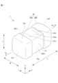
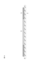
- FIG. 1 is an external perspective view of a multilayer ceramic capacitor according to an embodiment of the present invention
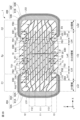
- FIG. 2 is a cross-sectional view taken along line II-II of FIG. 1, illustrating a schematic configuration of a laminate.
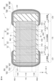
- 2 is a cross-sectional view taken along line II-II of FIG. 1, illustrating details of an internal electrode layer of the laminate.
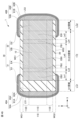
- FIG. 2B is a cross-sectional view taken along line III-III of FIG. 2A.
- FIG. 2B is a cross-sectional view along the line IVA-IVA of FIG. 2A, taken along the first internal electrode layer; IVB-IVB cross-sectional view of FIG. 2A, taken along the second internal electrode layer.
- 1 is a photograph showing a part of a cross section of a laminate.
- FIG. 6 is an enlarged photograph of a portion including a first central region and a second central region of the internal electrode layer in the photograph of FIG. 5.
- 6 is an enlarged photograph of a portion including the second and third regions of the internal electrode layer in the photograph of FIG. 5.
- FIG. 4 is a diagram showing measurement points when measuring the thicknesses of internal electrode layers and dielectric layers.
- FIG. 2 is a diagram illustrating an example of an enlarged SEM image of an exposed cross section of an inner layer portion. 2 is a schematic diagram showing a cross section of a dielectric sheet on which a conductive paste P1 is printed.
- FIG. 11 is a schematic diagram showing a cross section of the dielectric sheet of FIG. 10 on which a conductive paste P2 is printed.
- FIG. 1 is a schematic diagram showing a portion of a laminate sheet in which a portion that will become a first main surface side outer layer portion and a portion that will become a second main surface side outer layer portion are formed above and below a portion that will become an inner layer portion.
- FIG. 1 is an external perspective view of the multilayer ceramic capacitor 1 according to the embodiment.
- FIG. 2A is a cross-sectional view taken along line II-II of FIG. 1, and is a diagram for explaining the general configuration of the laminate.
- FIG. 2B is a cross-sectional view taken along line II-II of FIG. 1, and is a diagram for explaining details of the internal electrode layers of the laminate.
- FIG. 3 is a cross-sectional view taken along line III-III of FIG. 2A.
- FIG. 4A is a cross-sectional view taken along line IVA-IVA of FIG.
- FIG. 4B is a cross-sectional view taken along line IVB-IVB of FIG. 2A, and is a cross-sectional view taken along line 2 of the second internal electrode layer.
- the drawings may be drawn in a simplified schematic form to explain the contents of the invention, and the dimensional ratios of the depicted components or between the components may not match those described in the specification.
- components described in the specification may be omitted in the drawings, or may be drawn without showing the number of components.
- the number of internal electrode layers described in Figures 2A, 2B, and 3 is 12 for the sake of convenience, but this does not indicate the actual number of internal electrode layers 30.
- the terms used in this invention to specify shapes and geometric conditions, and their degrees, such as “parallel,” “orthogonal,” and “same,” as well as values of length and angle, are interpreted to include the range in which similar functions can be expected, without being bound by their strict meanings.
- the multilayer ceramic capacitor 1 has a substantially rectangular parallelepiped shape.
- the multilayer ceramic capacitor 1 includes a laminate 10 having a substantially rectangular parallelepiped shape, and a pair of external electrodes 40 arranged at a distance from each other on both ends of the laminate 10.
- arrow T indicates the stacking direction of the multilayer ceramic capacitor 1 and the laminate 10. This stacking direction T is also the thickness direction and height direction of the multilayer ceramic capacitor 1 and the laminate 10.
- arrow L indicates the length direction of the multilayer ceramic capacitor 1 and the laminate 10, which is perpendicular to the stacking direction T.
- arrow W indicates the width direction of the multilayer ceramic capacitor 1 and the laminate 10, which is perpendicular to the stacking direction T and the length direction L.
- a pair of external electrodes 40 are respectively disposed at one end and the other end of the length direction L of the laminate 10.
- FIG. 1 to 4B An XYZ orthogonal coordinate system is shown in Figures 1 to 4B and in Figures 5 and 8 described below.
- the length direction L of the multilayer ceramic capacitor 1 and the laminate 10 corresponds to the X direction.
- the width direction W of the multilayer ceramic capacitor 1 and the laminate 10 corresponds to the Y direction.
- the stacking direction T of the multilayer ceramic capacitor 1 and the laminate 10 corresponds to the Z direction.
- the cross sections shown in Figures 2A, 2B, and 8 are also referred to as LT cross sections.
- the cross section shown in Figure 3 is also referred to as WT cross section.
- the cross sections shown in Figures 4A and 4B are also referred to as LW cross sections.
- the laminate 10 includes a first main surface TS1 and a second main surface TS2 that face the stacking direction T, a first end surface LS1 and a second end surface LS2 that face the length direction L that is perpendicular to the stacking direction T, and a first side surface WS1 and a second side surface WS2 that face the width direction W that is perpendicular to the stacking direction T and the length direction L.
- the laminate 10 has a generally rectangular parallelepiped shape.
- the dimension of the laminate 10 in the length direction L is not necessarily longer than the dimension in the width direction W. It is preferable that the corners and ridges of the laminate 10 are rounded. A corner is a portion where three faces of the laminate intersect, and a ridge is a portion where two faces of the laminate intersect. Incidentally, unevenness may be formed on part or all of the surfaces constituting the laminate 10.
- the dimensions of the laminate 10 are not particularly limited, but if the dimension of the laminate 10 in the length direction L is the L dimension, it is preferable that the L dimension is 0.2 mm or more and 6 mm or less. If the dimension of the laminate 10 in the stacking direction T is the T dimension, it is preferable that the T dimension is 0.05 mm or more and 5 mm or less. If the dimension of the laminate 10 in the width direction W is the W dimension, it is preferable that the W dimension is 0.1 mm or more and 5 mm or less.
- the laminate 10 has an inner layer portion 11, and a first main surface side outer layer portion 12 and a second main surface side outer layer portion 13 arranged to sandwich the inner layer portion 11 in the stacking direction T.
- the inner layer portion 11 includes a plurality of dielectric layers 20 as a plurality of ceramic layers alternately stacked in the stacking direction T, and a plurality of internal electrode layers 30 as a plurality of internal conductor layers.
- the inner layer portion 11 includes the internal electrode layer 30 located closest to the first main surface TS1 in the stacking direction T to the internal electrode layer 30 located closest to the second main surface TS2.
- the multiple internal electrode layers 30 are arranged opposite each other via the dielectric layer 20.
- the inner layer portion 11 is a portion that generates electrostatic capacitance and essentially functions as a capacitor.
- the thickness of the inner layer portion 11 in the stacking direction T changes along the length direction L according to the shape of the internal electrode layer 30 located closest to the first main surface TS1 and the shape of the internal electrode layer 30 located closest to the second main surface TS2.
- the multiple dielectric layers 20 are made of a dielectric material.
- the dielectric material may be, for example, a dielectric ceramic containing components such as BaTiO3 , CaTiO3 , SrTiO3 , or CaZrO3 .
- the dielectric material may also be a material in which a subcomponent such as a Mn compound, an Fe compound, a Cr compound, a Co compound, or a Ni compound is added to the main components. It is particularly preferable that the dielectric material is a material containing BaTiO3 as the main component.
- the thickness of the dielectric layer 20 is preferably 0.2 ⁇ m or more and 10 ⁇ m or less.
- the number of dielectric layers 20 to be stacked is preferably 15 or more and 1200 or less.
- the number of dielectric layers 20 is the total number of the dielectric layers 20 in the inner layer portion 11 and the number of dielectric layers 20 in each of the first main surface side outer layer portion 12 and the second main surface side outer layer portion 13.
- the multiple internal electrode layers 30 include multiple first internal electrode layers 31 as multiple first internal conductor layers, and multiple second internal electrode layers 32 as multiple second internal conductor layers.
- the first internal electrode layers 31 and the second internal electrode layers 32 are alternately arranged in the stacking direction T with the dielectric layer 20 sandwiched therebetween.
- the first internal electrode layer 31 is extended to the first end face LS1.
- the second internal electrode layer 32 is extended to the second end face LS2.
- the first internal electrode layer 31 and the second internal electrode layer 32 may be collectively referred to as the internal electrode layer 30.
- the first internal electrode layer 31 has a first opposing portion EA and a first lead-out portion D1.
- the first opposing portion EA is a region facing the second internal electrode layer 32 with the dielectric layer 20 sandwiched therebetween, and is located inside the laminate 10.
- the first lead-out portion D1 is a portion that is led out from the first opposing portion EA to the first end face LS1, and is exposed at the first end face LS1.
- the second internal electrode layer 32 has a second opposing portion EB and a second lead-out portion D2.
- the second opposing portion EB is a region that faces the first internal electrode layer 31 with the dielectric layer 20 sandwiched therebetween, and is located inside the laminate 10.
- the second lead-out portion D2 is a portion that is led out from the second opposing portion EB to the second end face LS2, and is exposed at the second end face LS2.
- the first opposing portion EA and the second opposing portion EB face each other via the dielectric layer 20, forming a capacitance and exhibiting the characteristics of a capacitor.
- the shapes of the first opposing portion EA and the second opposing portion EB are not particularly limited, but are preferably rectangular. However, the corners of the rectangular shape may be rounded or the corners of the rectangular shape may be formed at an angle.
- the shapes of the first pull-out portion D1 and the second pull-out portion D2 are not particularly limited, but are preferably rectangular. However, the corners of the rectangular shape may be rounded or the corners of the rectangular shape may be formed at an angle.
- the dimension in the width direction W of the first opposing portion EA and the dimension in the width direction W of the first draw-out portion D1 may be the same dimension, or one of the dimensions may be smaller.
- the dimension in the width direction W of the second opposing portion EB and the dimension in the width direction W of the second draw-out portion D2 may be the same dimension, or one of the dimensions may be smaller.
- the first internal electrode layer 31 and the second internal electrode layer 32 are made of an appropriate conductive material, such as a metal such as Ni, Cu, Ag, Pd, or Au, or an alloy containing at least one of these metals. When an alloy is used, the first internal electrode layer 31 and the second internal electrode layer 32 may be made of, for example, an Ag-Pd alloy.
- each of the first internal electrode layer 31 and the second internal electrode layer 32 is preferably, for example, 0.2 ⁇ m or more and 2.0 ⁇ m or less.
- the total number of the first internal electrode layers 31 and the second internal electrode layers 32 is preferably 15 or more and 1000 or less.
- the first main surface side outer layer portion 12 is located on the first main surface TS1 side of the laminate 10.
- the first main surface side outer layer portion 12 is a collection of multiple dielectric layers 20 located between the first main surface TS1 and the internal electrode layer 30 closest to the first main surface TS1.
- the second main surface side outer layer portion 13 is located on the second main surface TS2 side of the laminate 10.
- the second main surface side outer layer portion 13 is a collection of multiple dielectric layers 20 located between the second main surface TS2 and the internal electrode layer 30 closest to the second main surface TS2.
- the dielectric layers 20 used in the first main surface side outer layer portion 12 and the second main surface side outer layer portion 13 may be the same as the dielectric layers 20 used in the internal layer portion 11.
- the laminate 10 has an opposing electrode portion 11E.
- the opposing electrode portion 11E is a portion where the first opposing portion EA of the first internal electrode layer 31 and the second opposing portion EB of the second internal electrode layer 32 face each other.
- the opposing electrode portion 11E is configured as a part of the inner layer portion 11.
- Figures 4A and 4B show the range of the width direction W and length direction L of the opposing electrode portion 11E.
- the opposing electrode portion 11E is also called the effective portion of the capacitor.
- the laminate 10 has a side surface outer layer portion.
- the side surface outer layer portion has a first side surface outer layer portion WG1 and a second side surface outer layer portion WG2.
- the first side surface outer layer portion WG1 is a portion including the dielectric layer 20 located between the opposing electrode portion 11E and the first side surface WS1.
- the second side surface outer layer portion WG2 is a portion including the dielectric layer 20 located between the opposing electrode portion 11E and the second side surface WS2.
- Figures 3, 4A, and 4B show the range of the width direction W of the first side surface outer layer portion WG1 and the second side surface outer layer portion WG2.
- the side surface outer layer portion is also called a W gap or a side gap.
- the laminate 10 has an end surface side outer layer portion.
- the end surface side outer layer portion has a first end surface side outer layer portion LG1 and a second end surface side outer layer portion LG2.
- the first end surface side outer layer portion LG1 is a portion that includes the dielectric layer 20 and the first lead portion D1, located between the opposing electrode portion 11E and the first end surface LS1.
- the first end surface side outer layer portion LG1 is an assembly of the portions of the multiple dielectric layers 20 on the first end surface LS1 side and the multiple first lead portions D1.
- the second end surface side outer layer portion LG2 is a portion that includes the dielectric layer 20 and the second lead portion D2, located between the opposing electrode portion 11E and the second end surface LS2.
- the second end surface side outer layer portion LG2 is an assembly of the portions of the multiple dielectric layers 20 on the second end surface LS2 side and the multiple second lead portions D2.
- 2A, 2B, 4A, and 4B show the range of the length direction L of the first end surface side outer layer portion LG1 and the second end surface side outer layer portion LG2.
- the end surface side outer layer portion is also called the L gap or end gap.
- the external electrode 40 has a first external electrode 40A arranged on the first end face LS1 side of the laminate 10, and a second external electrode 40B arranged on the second end face LS2 side of the laminate 10.
- the first external electrode 40A and the second external electrode 40B have the same basic configuration. Furthermore, the first external electrode 40A and the second external electrode 40B have shapes that are roughly plane-symmetrical with respect to a WT cross section at the center of the longitudinal direction L of the multilayer ceramic capacitor 1. Therefore, in the following, when it is not necessary to distinguish between the first external electrode 40A and the second external electrode 40B, the first external electrode 40A and the second external electrode 40B may be collectively referred to as the external electrodes 40.
- the first external electrode 40A is disposed on the first end face LS1.
- the first external electrode 40A is in contact with the first lead portion D1 of each of the first internal electrode layers 31 exposed on the first end face LS1. This allows the first external electrode 40A to be electrically connected to the first internal electrode layers 31.
- the first external electrode 40A may also be disposed on a portion of the first main surface TS1 and a portion of the second main surface TS2, as well as a portion of the first side surface WS1 and a portion of the second side surface WS2.
- the first external electrode 40A is formed to extend from the first end face LS1 to a portion of the first main surface TS1 and a portion of the second main surface TS2, as well as a portion of the first side surface WS1 and a portion of the second side surface WS2.
- the second external electrode 40B is disposed on the second end face LS2.
- the second external electrode 40B is in contact with the second lead-out portions D2 of the second internal electrode layers 32 exposed on the second end face LS2. This electrically connects the second external electrode 40B to the second internal electrode layers 32.
- the second external electrode 40B may also be disposed on a portion of the first main surface TS1 and a portion of the second main surface TS2, as well as a portion of the first side surface WS1 and a portion of the second side surface WS2.
- the second external electrode 40B is formed to extend from the second end face LS2 to a portion of the first main surface TS1 and a portion of the second main surface TS2, as well as a portion of the first side surface WS1 and a portion of the second side surface WS2.
- the first opposing portion EA of the first internal electrode layer 31 and the second opposing portion EB of the second internal electrode layer 32 face each other via the dielectric layer 20, forming a capacitance. Therefore, the characteristics of a capacitor are exhibited between the first external electrode 40A to which the first internal electrode layer 31 is connected and the second external electrode 40B to which the second internal electrode layer 32 is connected.
- the first external electrode 40A has a first base electrode layer 50A and a first plating layer 60A disposed on the first base electrode layer 50A.
- the second external electrode 40B has a second base electrode layer 50B and a second plating layer 60B disposed on the second base electrode layer 50B.
- the first base electrode layer 50A is disposed on the first end face LS1.
- the first base electrode layer 50A is connected to the first lead-out portion D1 of each of the multiple first internal electrode layers 31 exposed at the first end face LS1.
- the first base electrode layer 50A is formed to extend from the first end face LS1 to a portion of the first main surface TS1 and a portion of the second main surface TS2, as well as a portion of the first side surface WS1 and a portion of the second side surface WS2.
- the second base electrode layer 50B is disposed on the second end face LS2.
- the second base electrode layer 50B is in contact with the second lead portions D2 of each of the multiple second internal electrode layers 32 exposed at the second end face LS2.
- the second base electrode layer 50B is formed to extend from the second end face LS2 to a portion of the first main surface TS1 and a portion of the second main surface TS2, as well as a portion of the first side surface WS1 and a portion of the second side surface WS2.
- the first base electrode layer 50A and the second base electrode layer 50B include at least one selected from a baked layer, a thin film layer, etc.
- the first base electrode layer 50A and the second base electrode layer 50B of this embodiment are baked layers.
- the baked layer preferably contains a metal component and either a glass component or a ceramic component, or both.
- the metal component includes at least one selected from, for example, Cu, Ni, Ag, Pd, Ag-Pd alloy, Au, etc.
- the glass component includes at least one selected from, for example, B, Si, Ba, Mg, Al, Li, etc.
- the ceramic component may be the same type of ceramic material as the dielectric layer 20, or a different type of ceramic material.
- the ceramic component includes at least one selected from, for example, BaTiO 3 , CaTiO 3 , (Ba, Ca)TiO 3 , SrTiO 3 , CaZrO 3 , etc.
- the baked layer is formed by, for example, applying a conductive paste containing glass and metal to the laminate 10 and baking it.
- the baked layer can be formed by simultaneously baking the laminated chip before firing, which is the material of the laminate 10 having a plurality of internal electrodes and dielectric layers, and the conductive paste applied to the laminated chip.
- the baked layer may be formed by baking the laminate 10 after the laminated chip is fired to obtain the laminate 10 and then applying the conductive paste to the laminate 10 and baking it.
- it is preferable to form the baked layer by adding a ceramic material instead of the glass component and baking it. In that case, it is particularly preferable to use the same type of ceramic material as the dielectric layer 20 as the ceramic material to be added.
- the baked layer may be multiple layers.
- the thickness of the first base electrode layer 50A located on the first end surface LS1 in the length direction L is preferably, for example, about 3 ⁇ m or more and 200 ⁇ m or less at the center of the stacking direction T and width direction W of the first base electrode layer 50A.
- the thickness of the second base electrode layer 50B located on the second end surface LS2 in the length direction L is preferably, for example, about 3 ⁇ m or more and 200 ⁇ m or less at the center of the stacking direction T and width direction W of the second base electrode layer 50B.
- the thickness of the first base electrode layer 50A provided on this portion, corresponding to the stacking direction T is preferably, for example, about 3 ⁇ m or more and 25 ⁇ m or less at the center of the length direction L and width direction W of the first base electrode layer 50A provided on this portion.
- the thickness of the first base electrode layer 50A provided on this portion in the width direction W is preferably, for example, about 3 ⁇ m or more and 25 ⁇ m or less at the center of the first base electrode layer 50A provided on this portion in the length direction L and stacking direction T.
- the thickness of the second base electrode layer 50B provided on this portion is preferably, for example, about 3 ⁇ m or more and 25 ⁇ m or less at the center in the length direction L and width direction W of the second base electrode layer 50B provided on this portion.
- the thickness of the second base electrode layer 50B provided on this portion in the width direction W is preferably, for example, about 3 ⁇ m or more and 25 ⁇ m or less at the center of the length direction L and stacking direction T of the second base electrode layer 50B provided on this portion.
- the first base electrode layer 50A and the second base electrode layer 50B may be thin film layers.
- the thin film layers are layers on which metal particles are deposited.
- first base electrode layer 50A and the second base electrode layer 50B are formed as thin film layers, they are preferably formed by a thin film formation method such as sputtering or vapor deposition.
- a thin film formation method such as sputtering or vapor deposition.
- the first base electrode layer 50A of this embodiment is composed of a first thin film layer formed by a sputtered electrode.
- the second base electrode layer 50B is composed of a second thin film layer formed by a sputtered electrode.
- the first thin film layer formed by the sputtered electrode is disposed on a portion of the first side surface WS1 on the first main surface TS1.
- the second thin film layer formed by the sputtered electrode is disposed on a portion of the second side surface WS2 on the first main surface TS1.
- the thin film layer formed by the sputtered electrode preferably contains at least one metal selected from the group consisting of Mg, Al, Ti, W, Cr, Cu, Ni, Ag, Co, Mo, and V. This can increase the adhesive strength of the external electrode 40 to the laminate 10.
- the thin film layer may be a single layer, or may be formed of multiple layers. For example, it may be formed of a two-layer structure consisting of a layer of Ni-Cr alloy and a layer of Ni-Cu alloy.
- the first plating layer 60A is arranged to cover the first base electrode layer 50A.
- the second plating layer 60B is arranged to cover the second base electrode layer 50B.
- the first plating layer 60A and the second plating layer 60B may contain, for example, at least one selected from Cu, Ni, Sn, Ag, Pd, an Ag-Pd alloy, Au, etc.
- the first plating layer 60A and the second plating layer 60B may each be formed of multiple layers.
- the first plating layer 60A and the second plating layer 60B preferably have a two-layer structure in which a Sn plating layer is formed on a Ni plating layer.
- the first plating layer 60A has a first Ni plating layer 61A and a first Sn plating layer 62A located on the first Ni plating layer 61A.
- the second plating layer 60B has a second Ni plating layer 61B and a second Sn plating layer 62B located on the second Ni plating layer 61B.
- the Ni plating layer prevents the first and second underlying electrode layers 50A and 50B from being eroded by solder when mounting the multilayer ceramic capacitor 1.
- the Sn plating layer improves the wettability of the solder when mounting the multilayer ceramic capacitor 1, thereby making it easier to mount the multilayer ceramic capacitor 1.
- the thickness of each of the first Ni plating layer 61A, the first Sn plating layer 62A, the second Ni plating layer 61B, and the second Sn plating layer 62B is preferably 2 ⁇ m or more and 10 ⁇ m or less.
- the external electrode 40 of this embodiment may have, for example, a conductive resin layer containing conductive particles and a thermosetting resin.
- the conductive resin layer may be arranged so as to cover the baked layer.
- the conductive resin layer is arranged between the baked layer and the plating layer (first plating layer 60A, second plating layer 60B).
- the conductive resin layer may completely cover the baked layer, or may cover a portion of the baked layer.
- the conductive resin layer containing a thermosetting resin is more flexible than a conductive layer made of, for example, a plating film or a fired conductive paste. Therefore, even if the multilayer ceramic capacitor 1 is subjected to a physical shock or a shock caused by a thermal cycle, the conductive resin layer functions as a buffer layer. Therefore, the conductive resin layer suppresses the occurrence of cracks in the multilayer ceramic capacitor 1.
- the metal constituting the conductive particles may be Ag, Cu, Ni, Sn, Bi, or an alloy containing these.
- the conductive particles preferably contain Ag.
- the conductive particles are, for example, Ag metal powder. Ag has the lowest resistivity of all metals, making it suitable as an electrode material. In addition, Ag is a precious metal, so it is resistant to oxidation and has high weather resistance. Therefore, Ag metal powder is suitable as a conductive particle.
- the conductive particles may also be metal powder with an Ag-coated surface.
- the metal powder is preferably a powder of Cu, Ni, Sn, Bi or an alloy thereof. In order to make the base metal less expensive while maintaining the properties of Ag, it is preferable to use Ag-coated metal powder.
- the conductive particles may be Cu or Ni that has been subjected to an anti-oxidation treatment.
- the conductive particles may also be metal powder with a surface coating of Sn, Ni, or Cu.
- the metal powder is Ag, Cu, Ni, Sn, Bi, or an alloy powder of these.
- the shape of the conductive particles is not particularly limited.
- the conductive particles may be spherical, flat, or other shapes, but it is preferable to use a mixture of spherical metal powder and flat metal powder.
- the conductive particles contained in the conductive resin layer are primarily responsible for ensuring the electrical conductivity of the conductive resin layer. Specifically, when multiple conductive particles come into contact with each other, a conductive path is formed inside the conductive resin layer.
- the resin constituting the conductive resin layer may contain at least one selected from various known thermosetting resins, such as epoxy resin, phenolic resin, urethane resin, silicone resin, and polyimide resin.
- thermosetting resins such as epoxy resin, phenolic resin, urethane resin, silicone resin, and polyimide resin.
- epoxy resin which has excellent heat resistance, moisture resistance, and adhesion, is one of the most suitable resins.
- the resin of the conductive resin layer contains a hardener in addition to the thermosetting resin.
- the hardener of the epoxy resin may be various known compounds such as phenol-based, amine-based, acid anhydride-based, imidazole-based, active ester-based, and amide-imide-based compounds.
- the conductive resin layer may be formed of multiple layers.
- the thickness of the thickest part of the conductive resin layer is preferably 10 ⁇ m or more and 150 ⁇ m or less.
- the multilayer ceramic capacitor 1 may have a configuration including plating layers that are directly and electrically connected to the first internal electrode layer 31 and the second internal electrode layer 32.
- the plating layers may be formed after a catalyst is disposed on the surface of the laminate 10 as a pretreatment.
- the plating layer is preferably a multi-layer structure.
- the lower plating layer and the upper plating layer each preferably contain at least one metal selected from, for example, Cu, Ni, Sn, Pb, Au, Ag, Pd, Bi, or Zn, or an alloy containing these metals.
- the lower plating layer is more preferably formed using Ni, which has solder barrier properties.
- the upper plating layer is more preferably formed using Sn or Au, which has good solder wettability.
- the lower plating layer is preferably formed using Cu, which has good bonding properties with Ni.
- the upper plating layer may be formed as necessary, and the external electrode 40 may be composed of only the lower plating layer.
- the upper plating layer may be the outermost layer, or another plating layer may be formed on the surface of the upper plating layer.
- each plating layer that is placed without providing an underlying electrode layer is preferably 2 ⁇ m or more and 10 ⁇ m or less. It is preferable that the plating layer does not contain glass.
- the metal ratio per unit volume of the plating layer is preferably 99 volume % or more.
- the thickness of the base electrode layer can be reduced. Therefore, the dimension of the multilayer ceramic capacitor 1 in the height direction T can be reduced by the amount of the reduction in the thickness of the base electrode layer, thereby making it possible to reduce the height of the multilayer ceramic capacitor 1.
- the thickness of the dielectric layer 20 sandwiched between the first internal electrode layer 31 and the second internal electrode layer 32 can be increased by the amount of the reduction in the thickness of the base electrode layer, thereby improving the thickness of the element. In this way, by forming the plating layer directly on the laminate 10, the design freedom of the multilayer ceramic capacitor can be improved.
- the above is the basic configuration of the multilayer ceramic capacitor 1 according to the embodiment. If the lengthwise dimension of the multilayer ceramic capacitor 1 including the laminate 10 and the external electrodes 40 is taken as L dimension, then it is preferable that L dimension is 0.2 mm or more and 6 mm or less. If the dimension of the multilayer ceramic capacitor 1 in the stacking direction is taken as T dimension, then it is preferable that T dimension is 0.05 mm or more and 5 mm or less. If the widthwise dimension of the multilayer ceramic capacitor 1 is taken as W dimension, then it is preferable that W dimension is 0.1 mm or more and 5 mm or less.
- the internal electrode layer 30 contains hollow portions in which no metal material is present in addition to the metal material, and the ratio of the metal material in the internal electrode layer 30 is described as the coverage. Coverage is also referred to as the coverage rate of the internal electrode layer 30 with respect to the dielectric layer 20.
- the hollow portions in which no metal material is present may contain ceramic components such as dielectrics or glass components such as silica. Alternatively, they may be voids.
- the present embodiment will be described in detail with reference to Figures 1 to 7.
- the first main surface side inner layer portion 112 is the portion of the inner layer portion 11 on the first main surface TS1 side.
- the first main surface side inner layer portion 112 is, for example, the portion of the inner layer portion 11 on the first main surface TS1 side, and is a portion that includes at least the internal electrode layer 30 from the internal electrode layer 30 closest to the first main surface TS1 to the fifth internal electrode layer 30.
- the first main surface side inner layer portion 112 is, for example, 25% of the inner layer portion 11 on the first main surface TS1 side in the stacking direction.
- the second main surface side inner layer portion 113 is the portion of the inner layer portion 11 on the second main surface TS2 side.
- the second main surface side inner layer portion 113 is, for example, the portion of the inner layer portion 11 on the second main surface TS2 side, and is a portion that includes at least the internal electrode layer 30 from the internal electrode layer 30 closest to the second main surface TS2 to the fifth internal electrode layer 30.
- the second main surface side inner layer portion 113 is, for example, 25% of the inner layer portion 11 on the second main surface TS2 side in the stacking direction.
- the central inner layer portion 111 is a portion of the inner layer portion 11 that is located at the center of the stacking direction T of the laminate 10.
- the central inner layer portion 111 is, for example, a portion that includes at least the internal electrode layer 30 that is arranged in the central region of the stacking direction T of the laminate.
- the thicknesses of the central inner layer portion 111, the first main surface side internal layer portion 112, and the second main surface side internal layer portion 113 in the stacking direction T each vary along the length direction L in accordance with the shape of the internal electrode layer 30.
- the opposing electrode portion 11E of the inner layer portion 11 has a first side opposing electrode portion 112E, a second side opposing electrode portion 113E, and a central opposing electrode portion 111E.
- the first side surface side opposing electrode portion 112E is the portion of the opposing electrode portion 11E on the first side surface WS1 side.
- the first side surface side opposing electrode portion 112E is, for example, 25% of the opposing electrode portion 11E on the first side surface WS1 side in the width direction W.
- the first side surface side opposing electrode portion 112E has an area that overlaps with the first main surface side inner layer portion 112, the second main surface side inner layer portion 113, and a portion of the central inner layer portion 111.
- the second side surface side opposing electrode portion 113E is the portion of the opposing electrode portion 11E on the second side surface WS2 side.
- the second side surface side opposing electrode portion 113E is, for example, 25% of the opposing electrode portion 11E on the second side surface WS2 side in the width direction W.
- the second side surface side opposing electrode portion 113E has an area that overlaps with the first main surface side inner layer portion 112, the second main surface side inner layer portion 113, and part of the central inner layer portion 111.
- the central opposing electrode portion 111E is disposed between the first side surface opposing electrode portion 112E and the second side surface opposing electrode portion 113E.
- the central opposing electrode portion 111E is a portion of the opposing electrode portion 11E that includes the central region in the width direction W.
- the central opposing electrode portion 111E has an area that overlaps with the first main surface side inner layer portion 112, the second main surface side inner layer portion 113, and a portion of the central inner layer portion 111.
- the first opposing portion EA has a first region EA1, a second region EA2, and a first central region EA0.
- the first region EA1 is disposed on the first end face LS1 side.
- the second region EA2 is disposed on the second end face LS2 side.
- the first central region EA0 is located between the first region EA1 and the second region EA2.
- the first central region EA0 has a higher coverage than the first region EA1 and the second region EA2. Also, as shown in FIG. 2B, the first central region EA0 is disposed biased toward the outside of the laminate 10 compared to the first region EA1 and the second region EA2.
- the first central region EA0 of the first internal electrode layer 31 is arranged biased toward the first main surface TS1 side of the laminate 10 relative to the first region EA1 and the second region EA2.
- the first central region EA0 of the first internal electrode layer 31 is arranged biased toward the second main surface TS2 side of the laminate 10 relative to the first region EA1 and the second region EA2.
- the first central region EA0 may be arranged biased toward the outside of the laminate 10 relative to the first region EA1 and the second region EA2.
- the second opposing portion EB has a third region EB1, a fourth region EB2, and a second central region EB0.
- the third region EB1 is disposed on the second end face LS2 side.
- the fourth region EB2 is disposed on the first end face LS1 side.
- the second central region EB0 is located between the third region EB1 and the fourth region EB2.
- the second central region EB0 has a higher coverage than the third region EB1 and the fourth region EB2.
- the second central region EB0 is disposed biased toward the outside of the laminate 10 compared to the third region EB1 and the fourth region EB2.
- the second central region EB0 of the second internal electrode layer 32 is arranged biased toward the first main surface TS1 side of the laminate 10 relative to the third region EB1 and the fourth region EB2.
- the second central region EB0 of the second internal electrode layer 32 is arranged biased toward the second main surface TS2 side of the laminate 10 relative to the third region EB1 and the fourth region EB2.
- the second central region EB0 may be arranged biased toward the outside of the laminate 10 relative to the third region EB1 and the fourth region EB2.
- the first central region EA0 is preferably approximately parallel to a plane perpendicular to the stacking direction T.
- the first central region EA0, the first region EA1, and the second region EA2 preferably have approximately parallel portions. More preferably, the first central region EA0, the first region EA1, and the second region EA2 have approximately parallel portions to a plane perpendicular to the stacking direction T.
- the second central region EB0 is preferably approximately parallel to a plane perpendicular to the stacking direction T.
- the second central region EB0, the third region EB1, and the fourth region EB2 preferably have approximately parallel portions. More preferably, the second central region EB0, the third region EB1, and the fourth region EB2 have approximately parallel portions to a plane perpendicular to the stacking direction T.
- the distance Le0 of the first central region EA0 is shorter than the distance L1 between the first external electrode 40A and the second external electrode 40B.
- the distance Le0 of the second central region EB0 is shorter than the distance L1 between the first external electrode 40A and the second external electrode 40B.
- the distance of the first central region EA0 and the distance of the second central region EB0 are approximately equal, but this is not limited to this.
- the first central region EA0 and the second central region EB0 are disposed within the range of the distance L1 between the first external electrode 40A and the second external electrode 40B.
- the ends of the first central region EA0 and the second central region EB0 on the first end face LS1 side are disposed closer to the second end face LS2 side than the end 40AE on the stack center side of the first external electrode 40A disposed on the first main surface TS1 and the second main surface TS2.
- the ends of the first central region EA0 and the second central region EB0 on the second end face LS2 side are disposed closer to the first end face LS1 side than the end 40BE on the stack center side of the second external electrode 40B disposed on the first main surface TS1 and the second main surface TS2.
- the ends of the first region EA1 and the fourth region EB2 on the first end face LS1 side are disposed closer to the first end face LS1 than the end 40AE on the stack center side of the first external electrode 40A disposed on the first main surface TS1 and the second main surface TS2.
- the ends of the second region EA2 and the third region EB1 on the second end face LS2 side are disposed closer to the second end face LS2 than the end 40BE on the stack center side of the second external electrode 40B disposed on the first main surface TS1 and the second main surface TS2.
- the thickness of the first central region EA0 of the first internal electrode layer 31 in the stacking direction T is greater than the thickness of the first region EA1 and the thickness of the second region EA2 in the stacking direction T.
- the thickness of the first central region EA0 is preferably 101.6% to 111.3% of the thickness of the first region EA1 and the thickness of the second region EA2.
- the thickness of the first central region EA0 may be 101.6% to 109.8% of the thickness of the first region EA1 and the thickness of the second region EA2, and is more preferably 102.0% to 109.8%.
- it is even more preferably 103.0% to 109.8% of the thickness of the first region EA1 and the thickness of the second region EA2.
- the thickness of the second central region EB0 of the second internal electrode layer 32 in the stacking direction T is greater than the thickness of the third region EB1 and the thickness of the fourth region EB2.
- the thickness of the second central region EB0 is preferably 101.6% to 111.3% of the thickness of the third region EB1 and the thickness of the fourth region EB2.
- the thickness of the second central region EB0 may be 101.6% to 109.8% of the thickness of the third region EB1 and the thickness of the fourth region EB2, and is more preferably 102.0% to 109.8%.
- the thickness of the second central region EB0 is 103.0% to 109.8% of the thickness of the third region EB1 and the thickness of the fourth region EB2.
- the thickness of the first central region EA0 and the second central region EB0 is thicker than the thickness of the first region EA1, the second region EA2, the third region EB1, and the fourth region EB2.
- the thickness of the first central region EA0 and the second central region EB0 is preferably 101.6% to 111.3% of the thickness of the first region EA1, the second region EA2, the third region EB1, and the fourth region EB2.
- the thickness of the first central region EA0 and the second central region EB0 may be 101.6% to 109.8% of the thickness of the first region EA1, the second region EA2, the third region EB1, and the fourth region EB2, and is more preferably 102.0% to 109.8%.
- the thickness of the first central region EA0 and the second central region EB0 is 103.0% or more and 109.8% or less of the thickness of the first region EA1, the second region EA2, the third region EB1, and the fourth region EB2.
- the thickness of the first central region EA0 of the first internal electrode layer 31 in the stacking direction T is thicker than the thickness of the first lead-out portion D1.
- the thickness of the first central region EA0 is 101.6% or more and 111.3% or less of the thickness of the first drawer portion D1.
- the thickness of the first central region EA0 may be 101.6% or more and 109.8% or less of the thickness of the first drawer portion D1, and it is more preferable that the thickness of the first central region EA0 is 103.0% or more and 109.8% or less of the thickness of the first drawer portion D1.
- the thickness of the second central region EB0 of the second internal electrode layer 32 in the stacking direction T is thicker than the thickness of the second lead-out portion D2.
- the thickness of the second central region EB0 is 101.6% or more and 111.3% or less of the thickness of the second draw-out portion D2.
- the thickness of the second central region EB0 may be 101.6% or more and 109.8% or less of the thickness of the second draw-out portion D2, and it is more preferable that the thickness of the second central region EB0 is 103.0% or more and 109.8% or less of the thickness of the second draw-out portion D2.
- the first central area EA0 has a higher coverage than the first area EA1 and the second area EA2.
- the difference between the coverage of the first central area EA0 and the coverage of the first area EA1 and the coverage of the second area EA2 is 2.2 percentage points or more. It is also preferable that the difference between the coverage of the first central area EA0 and the coverage of the first area EA1 and the coverage of the second area EA2 is 2.2 percentage points or more and 11.4 percentage points or less.
- the difference between the coverage of the first central area EA0 and the coverage of the first area EA1 and the coverage of the second area EA2 is 3.0 percentage points or more and 11.4 percentage points or less, which is expected to produce a greater effect. It is even more preferable that the difference between the coverage of the first central area EA0 and the coverage of the first area EA1 and the coverage of the second area EA2 is 4.0 percentage points or more and 11.4 percentage points or less.
- the second central region EB0 has a higher coverage than the third region EB1 and the fourth region EB2.
- the difference between the coverage of the second central region EB0 and the coverage of the third region EB1 and the coverage of the fourth region EB2 is 2.2 percentage points or more. It is also preferable that the difference between the coverage of the second central region EB0 and the coverage of the third region EB1 and the coverage of the fourth region EB2 is 2.2 percentage points or more and 11.4 percentage points or less.
- the difference between the coverage of the second central region EB0 and the coverage of the third region EB1 and the coverage of the fourth region EB2 is 3.0 percentage points or more and 11.4 percentage points or less, which is expected to produce a greater effect. It is even more preferable that the difference between the coverage of the second central region EB0 and the coverage of the third region EB1 and the coverage of the fourth region EB2 is 4.0 percentage points or more and 11.4 percentage points or less.
- the coverage of the first central region EA0 and the second central region EB0 is higher than the coverage of the first region EA1, the second region EA2, the third region EB1 and the fourth region EB2. It is preferable that the coverage of the first central region EA0 and the second central region EB0 is 2.2 percentage points or more higher than the coverage of the first region EA1, the second region EA2, the third region EB1 and the fourth region EB2.
- the difference between the coverage of the first central region EA0 and the second central region EB0 and the coverage of the first region EA1, the second region EA2, the third region EB1 and the fourth region EB2 is 2.2 percentage points or more and 11.4 percentage points or less. It is more preferable that the difference between the coverage of the first central region EA0 and the second central region EB0 and the coverage of the first region EA1, the second region EA2, the third region EB1, and the fourth region EB2 is 3.0 percentage points or more and 11.4 percentage points or less, and a higher effect is expected.
- the difference between the coverage of the first central region EA0 and the second central region EB0 and the coverage of the first region EA1, the second region EA2, the third region EB1, and the fourth region EB2 is 4.0 percentage points or more and 11.4 percentage points or less.
- the first internal electrode layer 31 further has a first inclined portion FA1 connecting the first region EA1 and the first central region EA0, and a second inclined portion FA2 connecting the second region EA2 and the first central region EA0, as shown in FIG. 2B.
- the second internal electrode layer 32 further has a third inclined portion FB1 connecting the third region EB1 and the second central region EB0, and a fourth inclined portion FB2 connecting the fourth region EB2 and the second central region EB0.
- the distance Le3 in the length direction L of the first inclined portion FA1 and the distance Le4 in the length direction L of the second inclined portion FA2 are shorter than the distance Le0 in the length direction L of the first central region EA0.
- the distance Le4 in the length direction L of the third inclined portion FB1 and the distance Le3 in the length direction L of the fourth inclined portion FB2 are shorter than the distance Le0 in the length direction L of the second central region EB0.
- the distance Le1 in the length direction L of the first region EA1 and the distance Le2 in the length direction L of the second region EA2 may be shorter than the distance Le0 in the length direction L of the first central region EA0. Furthermore, the distance Le2 in the length direction L of the third region EB1 and the distance Le1 in the length direction L of the fourth region EB2 may be shorter than the distance Le0 in the length direction L of the second central region EB0.
- the ratio of the area of the first central region EA0 to the area of the first opposing portion EA is preferably 50% to 90% and may be 60% to 85%. More preferably, it is 70% to 80%, for example, 75%.
- the ratio of the area of the second central region EB0 to the area of the second opposing portion EB is preferably 50% to 90% and may be 60% to 85%. More preferably, it is 70% to 80%, for example, 75%.
- the distance Le3 in the length direction L between the first inclined portion FA1 and the fourth inclined portion FB2, and the distance Le4 in the length direction L between the second inclined portion FA2 and the third inclined portion FB1 are approximately equal, but this is not limited to this. It is preferable that the first central region EA0 and the second central region EB0 are arranged within the range of the distance L1 between the first external electrode 40A and the second external electrode 40B in the length direction L, and that the first inclined portion FA1, the second inclined portion FA2, the third inclined portion FB1, and the fourth inclined portion FB2 are arranged.
- this is not limited to the above.
- the inclination angle ⁇ of the first inclined portion FA1 relative to the first central region EA0 is 1° or more.
- the inclination angle ⁇ of the first inclined portion FA1 relative to the first central region EA0 may be 1° or more and 12° or less. More preferably, the inclination angle ⁇ of the first inclined portion FA1 relative to the first central region EA0 may be 2° or more and 10° or less.
- the inclination angle ⁇ of the second inclined portion FA2 relative to the first central region EA0 is 1° or more.
- the inclination angle ⁇ of the second inclined portion FA2 relative to the first central region EA0 may be 1° or more and 12° or less. More preferably, the inclination angle ⁇ of the second inclined portion FA2 relative to the first central region EA0 may be 2° or more and 10° or less.
- the inclination angle ⁇ of the third inclined portion FB1 relative to the second central region EB0 is 1° or more.
- the inclination angle ⁇ of the third inclined portion FB1 relative to the second central region EB0 may be 1° or more and 12° or less. More preferably, the inclination angle ⁇ of the third inclined portion FB1 relative to the second central region EB0 may be 2° or more and 10° or less.
- the inclination angle ⁇ of the fourth inclined portion FB2 relative to the second central region EB0 is 1° or more.
- the inclination angle ⁇ of the fourth inclined portion FB2 relative to the second central region EB0 may be 1° or more and 12° or less. More preferably, the inclination angle ⁇ of the fourth inclined portion FB2 relative to the second central region EB0 may be 2° or more and 10° or less.
- FIG. 2B shows the inclination angle ⁇ of the third inclined portion FB1 relative to the second central region EB0 in the second internal electrode layer 32 as a representative of the inclination angles ⁇ described above.
- inclination angle ⁇ 1° or more, preferably 2° or more, it is possible to secure an area for increasing the thickness of the internal electrode layer 30 in the first central region EA0 and the second central region EB0.
- inclination angle ⁇ to 12° or less, preferably 10° or less, it is possible to prevent the surface of the laminate 10 from expanding too much in the stacking direction T and protruding outward beyond the surface of the external electrode 40.
- the inclination angle ⁇ within the above-mentioned range, it becomes easy to set the relationship between the thickness of the first central region EA0 and the second central region and the thickness of the first region EA1, the second region EA2, the third region EB1, and the fourth region EB2 within the range of this embodiment. Furthermore, by setting the inclination angle ⁇ within the above-mentioned range, it becomes easy to set the relationship between the distance T0 at the center of the exposed portion of the laminate 10 (described below) and the maximum distance T1 at the covered portion of the laminate (described below) within the range of this embodiment (described below).
- the thickness of the first inclined portion FA1 gradually decreases toward the first end surface LS1, as shown in Figures 2A and 2B.
- the thickness of the second inclined portion FA2 gradually decreases toward the second end surface LS2, as shown in Figures 2A and 2B.
- the thickness of the third inclined portion FB1 gradually decreases toward the second end surface LS2, as shown in Figures 2A and 2B.
- the thickness of the fourth inclined portion FB2 gradually decreases toward the first end surface LS1, as shown in Figures 2A and 2B.
- the capacitance can be increased without increasing the size of the multilayer ceramic capacitor 1, and the occurrence of cracks in the laminate can be suppressed.
- the step distance ls1 in the stacking direction T between the first region EA1 and the first central region EA0 caused by the first inclined portion FA1 is at least twice the sum Tt of the thickness Te in the stacking direction T of the internal electrode layer 30 and the thickness Tc in the stacking direction T of the dielectric layer 20.
- the step distance ls1 in the stacking direction T between the first region EA1 and the first central region EA0 caused by the first inclined portion FA1 may be three times or more the sum Tt of the thickness Te in the stacking direction T of the internal electrode layer 30 and the thickness Tc in the stacking direction T of the dielectric layer 20.
- the step distance ls2 in the stacking direction T between the second region EA2 and the first central region EA0 caused by the second inclined portion FA2 is at least twice the sum Tt of the thickness Te in the stacking direction T of the internal electrode layer 30 and the thickness Tc in the stacking direction T of the dielectric layer 20.
- the step distance ls2 in the stacking direction T between the second region EA2 and the first central region EA0 caused by the second inclined portion FA2 may be three times or more the sum Tt of the thickness Te of the internal electrode layer 30 in the stacking direction T and the thickness Tc of the dielectric layer 20 in the stacking direction T.
- the step distance ls3 in the stacking direction T between the third region EB1 and the second central region EB0 caused by the third inclined portion FB1 is at least twice the sum Tt of the thickness Te in the stacking direction T of the internal electrode layer 30 and the thickness Tc in the stacking direction T of the dielectric layer 20.
- the step distance ls3 in the stacking direction T between the third region EB1 and the second central region EB0 caused by the third inclined portion FB1 may be three times or more the sum Tt of the thickness Te of the internal electrode layer 30 in the stacking direction T and the thickness Tc of the dielectric layer 20 in the stacking direction T.
- the step distance ls4 in the stacking direction T between the fourth region EB2 and the second central region EB0 caused by the fourth inclined portion FB2 is at least twice the sum Tt of the thickness Te in the stacking direction T of the internal electrode layer 30 and the thickness Tc in the stacking direction T of the dielectric layer 20.
- the step distance ls4 in the stacking direction T between the fourth region EB2 and the second central region EB0 caused by the fourth inclined portion FB2 may be three times or more the sum Tt of the thickness Te of the internal electrode layer 30 in the stacking direction T and the thickness Tc of the dielectric layer 20 in the stacking direction T.
- the thickness Te of the internal electrode layer 30 in the stacking direction T is the thickness of the internal electrode layer 30 in the first central region EA0 and the second central region EB0 in the stacking direction T.
- the thickness Tc of the dielectric layer 20 in the stacking direction T is the thickness of the dielectric layer 20 arranged between the first central region EA0 and the second central region EB0 in the stacking direction T.
- the step distance ls1 in the stacking direction T between the first region EA1 and the first central region EA0 caused by the first inclined portion FA1 may be 1.6 ⁇ m or more, or may be 1.6 ⁇ m or more and 16 ⁇ m or less. For example, it may be 2.9 ⁇ m or more and 14.8 ⁇ m or less.
- the step distance ls2 in the stacking direction T between the second region EA2 and the first central region EA0 caused by the second inclined portion FA2 may be 1.6 ⁇ m or more, or may be 1.6 ⁇ m or more and 16 ⁇ m or less. For example, it may be 2.9 ⁇ m or more and 14.8 ⁇ m or less.
- the step distance ls3 in the stacking direction T between the third region EB1 and the second central region EB0 caused by the third inclined portion FB1 may be 1.6 ⁇ m or more, or may be 1.6 ⁇ m or more and 16 ⁇ m or less. For example, it may be 2.9 ⁇ m or more and 14.8 ⁇ m or less.
- the step distance ls4 in the stacking direction T between the fourth region EB2 and the second central region EB0 caused by the fourth inclined portion FB2 may be 1.6 ⁇ m or more, or may be 1.6 ⁇ m or more and 16 ⁇ m or less. For example, it may be 2.9 ⁇ m or more and 14.8 ⁇ m or less.
- the first internal electrode layer 31 further has a fifth inclined portion FA3 located at the first lead-out portion D1.
- the second internal electrode layer 32 further has a sixth inclined portion FB3 located at the second lead-out portion D2.
- moisture such as plating solution may penetrate from the surface of the external electrode 40 through the thickness direction of the external electrode 40.
- the end of the internal electrode layer 30 can be positioned closer to the center in the height direction of the laminate 10, where the thickness of the external electrode 40 in the length direction L is usually likely to be large. This makes it possible to increase the capacitance and ensure moisture resistance without increasing the size of the multilayer ceramic capacitor 1.
- the distance from the end of the internal electrode layer 30 to the opposing portion of the internal electrode layer 30 can be increased. This makes it possible to increase the distance of the path for moisture to penetrate to the opposing portion of the internal electrode layer 30. Therefore, it is possible to increase the capacitance and ensure moisture resistance without increasing the size of the multilayer ceramic capacitor 1.
- the inclination angle ⁇ of the first inclined portion FA1 and the second inclined portion FA2 is smaller than the inclination angle ⁇ 2 of the fifth inclined portion FA3.
- the inclination angle ⁇ of the fifth inclined portion FA3 is larger than the inclination angle ⁇ of the first inclined portion FA1 and the second inclined portion FA2.
- the inclination angle ⁇ 2 of the fifth inclined portion FA3 relative to the first central area EA0 or the first area EA1 may be, for example, 10° or more, or 15° or more.
- the inclination angle ⁇ of the third inclined portion FB1 and the fourth inclined portion FB2 is smaller than the inclination angle ⁇ 2 of the sixth inclined portion FB3.
- the inclination angle ⁇ 2 of the sixth inclined portion FB3 is larger than the inclination angle ⁇ of the third inclined portion FB1 and the fourth inclined portion FB2.
- the inclination angle ⁇ 2 of the sixth inclined portion FB3 relative to the second central region EB0 or the third region EB1 may be, for example, 10° or more, or 15° or more.
- FIG. 2B shows the inclination angle ⁇ 2 of the sixth inclined portion FB3 relative to the second central region EB0 and the third region EB1 in the second internal electrode layer 32 as a representative of the inclination angle ⁇ 2 described above.
- the laminate 10 has an exposed portion Ep exposed from the first external electrode 40A and the second external electrode 40B, a first covered portion C1 covered by the first external electrode, and a second covered portion C2 covered by the second external electrode 40B.
- the distance L1 in the length direction L of the exposed portion Ep exposed from the first external electrode 40A and the second external electrode 40B corresponds to the distance L1 between the first external electrode 40A and the second external electrode 40B.
- the distance T0 in the stacking direction T at the center in the length direction L of the exposed portion Ep is longer than the maximum distance T1, which is the maximum value of the distance in the stacking direction T connecting the first main surface TS1 side surface and the second main surface TS2 side surface of the first covering portion C1. Also, in this embodiment, the distance T0 in the stacking direction T at the center in the length direction L of the exposed portion Ep is longer than the maximum distance T1, which is the maximum value of the distance in the stacking direction T connecting the first main surface TS1 side surface and the second main surface TS2 side surface of the second covering portion C2. Note that, in this embodiment, the distance T0 in the stacking direction T at the center in the length direction L of the exposed portion Ep is the maximum distance in the stacking direction T of the exposed portion Ep of the laminate 10.
- the distance T0 in the stacking direction T at the center of the length direction L of the exposed portion Ep is 103.2% or less of the maximum distance T1 in the stacking direction T connecting the first main surface TS1 side surface and the second main surface TS2 side surface of the first covering portion C1.
- the distance T0 in the stacking direction T at the center of the length direction L of the exposed portion Ep may be 100.6% or more and 103.2% or less of the maximum distance T1 in the stacking direction T connecting the first main surface TS1 side surface and the second main surface TS2 side surface of the first covering portion C1.
- the distance T0 in the stacking direction T at the center of the length direction L of the exposed portion Ep may be 100.6% or more and 102.7% or less of the maximum distance T1 in the stacking direction T connecting the first main surface TS1 side surface and the second main surface TS2 side surface of the first covering portion C1.
- the distance in the stacking direction T connecting the planar portion PA1 and the planar portion PB1 is the maximum distance T1 described above.
- the distance T0 in the stacking direction T at the center of the length direction L of the exposed portion Ep is 103.2% or less of the maximum distance T1 in the stacking direction T connecting the first main surface TS1 side surface and the second main surface TS2 side surface of the second covering portion C2.
- the distance T0 in the stacking direction T at the center of the length direction L of the exposed portion Ep may be 100.6% or more and 103.2% or less of the maximum distance T1 in the stacking direction T connecting the first main surface TS1 side surface and the second main surface TS2 side surface of the second covering portion C2.
- the distance T0 in the stacking direction T at the center of the length direction L of the exposed portion Ep may be 100.6% or more and 102.7% or less of the maximum distance T1 in the stacking direction T connecting the first main surface TS1 side surface and the second main surface TS2 side surface of the second covering portion C2.
- the distance in the stacking direction T connecting the planar portion PA2 and the planar portion PB2 is the maximum distance T1 described above.
- the distance T0 in the stacking direction T at the center of the length direction L of the exposed portion Ep is shorter than the maximum distance T2, which is the maximum value of the distance in the stacking direction T connecting the first main surface TS1 side surface and the second main surface TS2 side surface of the first external electrode 40A. Also, the distance T0 in the stacking direction T at the center of the length direction L of the exposed portion Ep is shorter than the maximum distance T2, which is the maximum value of the distance in the stacking direction T connecting the first main surface TS1 side surface and the second main surface TS2 side surface of the second external electrode 40B.
- the ratio of the thickness in the stacking direction T of the first central region EA0 of the first internal electrode layer 31 to the thickness in the stacking direction T of the first region EA1 may be set to be greater than the ratio of the distance T0 in the stacking direction T at the center in the length direction L of the exposed portion Ep of the laminate 10 to the maximum distance T1 in the stacking direction T of the first covered portion C1 of the laminate 10.
- the ratio of the thickness in the stacking direction T of the second central region EB0 of the second internal electrode layer 32 to the thickness in the stacking direction T of the third region EB1 may be set to be greater than the ratio of the distance T0 in the stacking direction T at the center in the length direction L of the exposed portion Ep of the laminate 10 to the maximum distance T1 in the stacking direction T of the second covered portion C2 of the laminate 10.
- the first principal surface TS1 has a first exposed surface EpsA exposed from the first external electrode 40A and the second external electrode 40B, a first covered surface C1sA covered by the first external electrode 40A, and a second covered surface C2sA covered by the second external electrode 40B.
- the first exposed surface EpsA has a first flat surface PA0 parallel to the stacking direction T, a first inclined surface FC1 connecting the first flat surface PA0 and the first covered surface C1sA, and a second inclined surface FC2 connecting the first flat surface PA0 and the second covered surface C2sA.
- a planar portion PA1 is formed on the center side of the stack of the first covered surface C1sA, and the first inclined surface FC1 connects the first flat surface PA0 and the planar portion PA1.
- a planar portion PA2 is formed on the center side of the stack of the second covered surface C2sA, and the second inclined surface FC2 connects the first flat surface PA0 and the planar portion PA2.
- the first main surface TS1 of this embodiment has a planar portion PA1 on the first end surface LS1 side, a planar portion PA2 on the second end surface LS2 side, a first flat surface PA0 disposed between planar portion PA1 and planar portion PA2 and protruding from planar portion PA1 and planar portion PA2, a first inclined surface FC1 connecting the first flat surface PA0 and planar portion PA1, and a second inclined surface FC2 connecting the first flat surface PA0 and planar portion PA2.
- the second principal surface TS2 has a second exposed surface EpsB exposed from the first external electrode 40A and the second external electrode 40B, a third covered surface C1sB covered by the first external electrode 40A, and a fourth covered surface C2sB covered by the second external electrode.
- the second exposed surface EpsB has a second flat surface PB0 parallel to the stacking direction T, a third inclined surface FC3 connecting the second flat surface PB0 and the third coated surface C1sB, and a fourth inclined surface FC4 connecting the second flat surface PB0 and the fourth coated surface C2sB.
- a flat portion PB1 is formed on the central side of the stack of the third coated surface C1sB
- the third inclined surface FC3 connects the second flat surface PB0 and the flat portion PB1.
- a flat portion PB2 is formed on the central side of the stack of the fourth coated surface C2sB
- the fourth inclined surface FC4 connects the second flat surface PB0 and the flat portion PB2.
- the second main surface TS2 of this embodiment has a planar portion PB1 on the first end surface LS1 side, a planar portion PB2 on the second end surface LS2 side, a second planar surface PB0 disposed between planar portion PB1 and planar portion PB2 and protruding from planar portion PB1 and planar portion PB2, a third inclined surface FC3 connecting the second planar surface PB0 and planar portion PB1, and a fourth inclined surface FC4 connecting the second planar surface PB0 and planar portion PB2.
- the distance Lt1 in the length direction L of the first inclined surface FC1 and the distance Lt2 in the length direction L of the second inclined surface FC2 are shorter than the distance Lt0 in the length direction L of the first flat surface PA0.
- the distance Lt1 in the length direction L of the third inclined surface FC3 and the distance Lt2 in the length direction L of the fourth inclined surface FC4 are shorter than the distance Lt0 in the length direction L of the second flat surface PB0.
- the distance Lt0 of the first flat surface PA0 in the length direction L is shorter than the distance L1 between the first external electrode 40A and the second external electrode 40B. Also, the distance Lt0 of the second flat surface PB0 in the length direction L is shorter than the distance L1 between the first external electrode 40A and the second external electrode 40B. Thus, it is preferable that the distance Lt0 of the length direction L of the first flat surface PA0 and the second flat surface PB0 is arranged within the range of the distance L1 between the first external electrode 40A and the second external electrode 40B in the length direction L.
- the end portion 40AE of the first external electrode 40A may be located on the first inclined surface FC1 and the third inclined surface FC3, or may be located on the flat portion PA1 and the flat portion PB1 on the first end surface LS1 side from the first inclined surface FC1 and the third inclined surface FC3.
- the end 40BE of the second external electrode 40B may be located on the second inclined surface FC2 and the fourth inclined surface FC4, or may be located on the flat surface PA2 and the flat surface PB2 closer to the second end surface LS2 than the second inclined surface FC2 and the fourth inclined surface FC4.
- the end 40AE of the first external electrode 40A is located near the boundary between the first inclined surface FC1 and the flat surface PA1, and near the boundary between the third inclined surface FC3 and the flat surface PB1.
- the end 40BE of the second external electrode 40B is located near the boundary between the second inclined surface FC2 and the flat surface PA2, and near the boundary between the fourth inclined surface FC4 and the flat surface PB2.
- the inclination angle ⁇ of the first inclined surface FC1 relative to the first flat surface PA0 is 1° or more.
- the inclination angle ⁇ of the first inclined surface FC1 relative to the first flat surface PA0 may be 1° or more and 10° or less. More preferably, the inclination angle ⁇ of the first inclined surface FC1 relative to the first flat surface PA0 may be 2° or more and 5° or less.
- the inclination angle ⁇ of the second inclined surface FC2 relative to the first flat surface PA0 is 1° or more.
- the inclination angle ⁇ of the second inclined surface FC2 relative to the first flat surface PA0 may be 1° or more and 10° or less. More preferably, the inclination angle ⁇ of the second inclined surface FC2 relative to the first flat surface PA0 may be 2° or more and 5° or less.
- the inclination angle ⁇ of the third inclined surface FC3 relative to the second flat surface PB0 is 1° or more.
- the inclination angle ⁇ of the third inclined surface FC3 relative to the second flat surface PB0 may be 1° or more and 10° or less. More preferably, the inclination angle ⁇ of the third inclined surface FC3 relative to the second flat surface PB0 may be 2° or more and 5° or less.
- the inclination angle ⁇ of the fourth inclined surface FC4 relative to the second flat surface PB0 is 1° or more.
- the inclination angle ⁇ of the fourth inclined surface FC4 relative to the second flat surface PB0 may be 1° or more and 10° or less. More preferably, the inclination angle ⁇ of the fourth inclined surface FC4 relative to the second flat surface PB0 may be 2° or more and 5° or less.
- FIG. 2A shows the inclination angle ⁇ of the fourth inclined surface FC4 on the second main surface TS2 relative to the second flat surface PB0 as a representative of the inclination angles ⁇ described above.
- inclination angle ⁇ 1° or more, preferably 2° or more, it is possible to secure an area for increasing the thickness of the internal electrode layer 30 in the first central region EA0 and the second central region EB0.
- inclination angle ⁇ to 10° or less, preferably 5° or less, it is possible to prevent the surface of the laminate 10 from expanding too much in the stacking direction T and protruding outward beyond the surface of the external electrode 40.
- the inclination angle ⁇ within the above-mentioned range, it becomes easy to set the relationship between the thickness of the first central region EA0 and the second central region and the thickness of the first region EA1, the second region EA2, the third region EB1, and the fourth region EB2 within the range of this embodiment. Furthermore, by setting the inclination angle ⁇ within the above-mentioned range, it becomes easy to set the relationship between the distance T0 at the center of the exposed portion of the laminate 10 and the maximum distance T1 at the covered portion of the laminate within the range of this embodiment.
- the first flat surface PA0 is preferably approximately parallel to a plane perpendicular to the stacking direction T.
- the first flat surface PA0 is preferably approximately parallel to the planar portion PA1 and the planar portion PA2. More preferably, the first flat surface PA0 is approximately parallel to the planar portion PA1 and the planar portion PA2.
- the second flat surface PB0 is preferably approximately parallel to a plane perpendicular to the stacking direction T.
- the second flat surface PB0 is preferably approximately parallel to the planar portion PB1 and the planar portion PB2. More preferably, the second flat surface PB0 is approximately parallel to the plane perpendicular to the stacking direction T.
- the step distance tf in the stacking direction T between the first flat surface PA0 formed by the first inclined surface FC1 and the second inclined surface FC2 and the planar portions PA1 and PA2, i.e., the protrusion height tf (one-sided bulge dimension of the laminate) of the first flat surface PA0 formed by the first inclined surface FC1 and the second inclined surface FC2, is smaller than the thickness tg in the stacking direction T of the first external electrode 40A and the second external electrode 40B arranged on the first main surface TS1.
- the step distance tf in the stacking direction T between the second flat surface PB0 and the flat portions PB1 and PB2, which is formed by the third inclined surface FC3 and the fourth inclined surface FC4, i.e., the protruding height tf (one-side bulge dimension of the laminate) of the second flat surface PB0 formed by the third inclined surface FC3 and the fourth inclined surface FC4, is preferably smaller than the thickness tg in the stacking direction T of the first external electrode 40A and the second external electrode 40B arranged on the second main surface TS2.
- the raised height tf of the first flat surface PA0 formed by the first inclined surface FC1 and the second inclined surface FC2 is preferably 2.9 ⁇ m or more and 14.8 ⁇ m or less.
- the raised height tf of the first flat surface PA0 formed by the first inclined surface FC1 and the second inclined surface FC2 may be 2.9 ⁇ m or more and 12.6 ⁇ m or less.
- the raised height tf of the second flat surface PB0 formed by the third inclined surface FC3 and the fourth inclined surface FC4 is preferably 2.9 ⁇ m or more and 14.8 ⁇ m or less.
- the raised height tf of the second flat surface PB0 formed by the third inclined surface FC3 and the fourth inclined surface FC4 may be 2.9 ⁇ m or more and 12.6 ⁇ m or less.
- the protruding height tf of the first flat surface PA0 formed by the first inclined surface FC1 and the second inclined surface FC2 is at least twice the sum Tt of the thickness Te of the internal electrode layer 30 in the stacking direction T and the thickness Tc of the dielectric layer 20 in the stacking direction T. Furthermore, the protruding height tf of the first flat surface PA0 formed by the first inclined surface FC1 and the second inclined surface FC2 may be three times or more the sum Tt of the thickness Te of the internal electrode layer 30 in the stacking direction T and the thickness Tc of the dielectric layer 20 in the stacking direction T.
- the protruding height tf of the second flat surface PB0 formed by the third inclined surface FC3 and the fourth inclined surface FC4 is at least twice the sum Tt of the thickness Te of the internal electrode layer 30 in the stacking direction T and the thickness Tc of the dielectric layer 20 in the stacking direction T. Furthermore, the protruding height tf of the second flat surface PB0 formed by the third inclined surface FC3 and the fourth inclined surface FC4 may be three times or more the sum Tt of the thickness Te of the internal electrode layer 30 in the stacking direction T and the thickness Tc of the dielectric layer 20 in the stacking direction T.
- the thickness t01 in the stacking direction T in the first flat surface PA0 region of the first main surface side outer layer portion 12 is smaller than the thickness t11 in the stacking direction T in the first coated surface C1sA region of the first main surface side outer layer portion 12 and the thickness t21 in the stacking direction T in the second coated surface C2sA region of the first main surface side outer layer portion 12.
- the thickness t02 in the stacking direction T in the second flat surface PB0 region of the second main surface side outer layer portion 13 is smaller than the thickness t12 in the stacking direction T in the first coated surface C1sA region of the second main surface side outer layer portion 13 and the thickness t22 in the stacking direction T in the second coated surface C2sA region of the second main surface side outer layer portion 13.
- This increases the capacitance without increasing the size of the multilayer ceramic capacitor 1, while at the same time ensuring a longer distance between the external electrode 40 and the internal electrode layer 30, thereby suppressing the concentration of the electric field, thereby preventing a decrease in the reliability of the multilayer ceramic capacitor 1 due to electric field concentration.
- flat surfaces as part of the surface of the laminate 10 are arranged in a raised manner on both the first main surface TS1 and the second main surface TS2, but a flat surface as part of the surface of the laminate 10 may be arranged in a raised manner on either the first main surface TS1 or the second main surface TS2.
- the thickness in the length direction L of the first external electrode 40A at the center in the stacking direction T is thicker than the thickness in the length direction L of the first external electrode 40A on the first main surface TS1 side in the stacking direction T and the thickness in the length direction L of the first external electrode 40A on the second main surface TS2 side in the stacking direction T.
- the thickness in the length direction L of the first external electrode 40A at the center in the width direction W is thicker than the thickness in the length direction L of the first external electrode 40A on the first side surface WS1 side in the width direction W and the thickness in the length direction L of the first external electrode 40A on the second side surface WS2 side in the width direction W.
- the thickness in the length direction L of the second external electrode 40B at the center in the stacking direction T is thicker than the thickness in the length direction L of the second external electrode 40B on the first main surface TS1 side in the stacking direction T and the thickness in the length direction L of the second external electrode 40B on the second main surface TS2 side in the stacking direction T.
- the thickness in the length direction L of the second external electrode 40B at the center in the width direction W is thicker than the thickness in the length direction L of the second external electrode 40B on the first side surface WS1 side in the width direction W and the thickness in the length direction L of the second external electrode 40B on the second side surface WS2 side in the width direction W.
- the first internal electrode layer 31 of this embodiment preferably has the first main surface side inner layer portion 112, the second main surface side inner layer portion 113, and the above-mentioned first central region EA0 in the central inner layer portion 111, which has higher coverage and is thicker than the first region EA1 and the second region EA2.
- the first internal electrode layer 31 may have the above-mentioned first central region EA0 in at least one portion of the first main surface side inner layer portion 112 or the second main surface side inner layer portion 113, which has higher coverage and is thicker than the first region EA1 and the second region EA2. This also provides the effect of increasing the capacitance without increasing the size of the multilayer ceramic capacitor 1.
- the second internal electrode layer 32 of this embodiment preferably has the above-mentioned second central region EB0 in the first main surface side inner layer portion 112, the second main surface side inner layer portion 113, and the central inner layer portion 111, which has higher coverage and is thicker than the third region EB1 and the fourth region EB2.
- the second internal electrode layer 32 may have the above-mentioned second central region EB0 in at least one portion of the first main surface side inner layer portion 112 or the second main surface side inner layer portion 113, which has higher coverage and is thicker than the third region EB1 and the fourth region EB2. This also provides the effect of increasing the capacitance without increasing the size of the multilayer ceramic capacitor 1.
- the first inclined portion FA1, the second inclined portion FA2, the third inclined portion FB1, the fourth inclined portion FB2, the fifth inclined portion FA3, and the sixth inclined portion FB3 are arranged in the first main surface side inner layer portion 112 and the second main surface side inner layer portion 113.
- the first inclined portion FA1, the second inclined portion FA2, the third inclined portion FB1, the fourth inclined portion FB2, the fifth inclined portion FA3, and the sixth inclined portion FB3 may be arranged in at least one portion of the first main surface side inner layer portion 112 or the second main surface side inner layer portion 113.
- the first internal electrode layer 31 of this embodiment preferably has the first side facing electrode portion 112E, the second side facing electrode portion 113E, and the above-mentioned first central region EA0 in the central facing electrode portion 111E, which has higher coverage and is thicker than the first region EA1 and the second region EA2.
- the present disclosure is not limited to this, by having the above-mentioned first central region EA0 in the first side facing electrode portion 112E and the second side facing electrode portion 113E in addition to the central facing electrode portion 111E, which has higher coverage and is thicker than the first region EA1 and the second region EA2, it is possible to ensure the area of the first central region EA0 with high coverage, and therefore it is possible to further increase the capacitance without increasing the size of the multilayer ceramic capacitor 1.
- At least the central opposing electrode portion 111E may have the above-mentioned first central region EA0, which has a higher coverage and a greater thickness than the first region EA1 and the second region EA2.
- the second internal electrode layer 32 of this embodiment preferably has the first side surface facing electrode portion 112E, the second side surface facing electrode portion 113E, and the above-mentioned second central region EB0 in the central facing electrode portion 111E, which has higher coverage and is thicker than the third region EB1 and the fourth region EB2.
- the first side surface facing electrode portion 112E and the second side surface facing electrode portion 113E also have the above-mentioned second central region EB0 in which the coverage is higher and the thickness is thicker than the third region EB1 and the fourth region EB2, so that the area of the second central region EB0 with high coverage can be secured, thereby making it possible to further increase the capacitance without increasing the size of the multilayer ceramic capacitor 1.
- At least the central opposing electrode portion 111E may have the above-mentioned second central region EB0, which has a higher coverage and a greater thickness than the third region EB1 and the fourth region EB2.
- Figures 5 to 7 show examples of enlarged images of a cross section of the multilayer ceramic capacitor 1 of this embodiment observed with an optical microscope.
- FIG. 5 is a photograph showing a portion of a cross section of the laminate 10.
- FIG. 5 is a cross-sectional photograph showing the upper right region of the laminate 10 in FIG. 2B, and includes a portion of the first main surface side inner layer portion 112.
- the upper left region, lower right region, and lower left region of the laminate 10 in FIG. 2B are basically configured in a manner that is symmetrical from left to right, from top to bottom, and rotationally symmetrical with the upper right region shown in FIG. 5. Therefore, the photograph in FIG. 5 will be used to represent these regions for the explanation.
- FIG. 5 is a cross-sectional photograph of the laminate 10 in a state in which the external electrode 40 is not arranged.
- FIG. 6 is an enlarged photograph of portion VI in the photograph of FIG. 5, which is a portion including the first central region EA0 of the first internal electrode layer 31 and the second central region EB0 of the second internal electrode layer 32.
- FIG. 7 is an enlarged photograph of portion VII in the photograph of FIG. 5, which is a portion including the second region EA2 of the first internal electrode layer 31 and the third region EB1 of the second internal electrode layer 32.
- the optical microscope photograph in Figure 5 confirms that the laminate 10 has an inner layer portion 11 and a first main surface side outer layer portion 12 composed of a dielectric layer 20.
- the optical microscope photograph in FIG. 5 confirms that in the inner layer portion 11, a first internal electrode layer 31 and a second internal electrode layer 32 are arranged as the internal electrode layers 30.
- the optical microscope photographs in FIG. 6 and FIG. 7 confirm that a dielectric layer 20 is arranged between the multiple internal electrode layers 30.
- the laminate 10 has an area (EA, EB area) where the first opposing portion EA of the first internal electrode layer 31 and the second opposing portion EB of the second internal electrode layer 32 are present, and an area (D2 area) where the second lead-out portion D2 of the second internal electrode layer 32 is present.
- the laminate 10 has a region in which the first central region EA0 of the first internal electrode layer 31 and the second central region EB0 of the second internal electrode layer 32 exist, indicated by the range of distance Le0, a region in which the second region EA2 of the first internal electrode layer 31 and the third region EB1 of the second internal electrode layer 32 exist, indicated by the range of distance Le2, and a region in which the second inclined portion FA2 of the first internal electrode layer 31 and the third inclined portion FB1 of the second internal electrode layer 32 exist, indicated by the range of distance Le4. It can also be seen that a sixth inclined portion FB3 exists in the region of the second lead-out portion D2 of the second internal electrode layer 32.
- the first main surface TS1 of the laminate 10 has a first flat surface PA0 parallel to the stacking direction T, a planar portion PA2, and a second inclined surface FC2 connecting the first flat surface PA0 and the planar portion PA2.
- the coverage of the first central region EA0 and the second central region EB0 is compared with that of the second region EA2 and the third region EB1 using FIG. 6 and FIG. 7.
- the black linear portions extending in the left-right direction indicate the dielectric layer 20
- the white linear portions extending in the left-right direction indicate the internal electrode layer 30.
- the black portions present in the middle of the white linear portions extending in the left-right direction indicate the void portions V where no metal material is present. Therefore, the more white portions there are, the higher the coverage. It can be seen that there are fewer void portions V in FIG. 6 compared to FIG. 7. Therefore, it can be seen that the coverage of the first central region EA0 and the second central region EB0 shown in FIG. 6 is higher than the coverage of the second region EA2 and the third region EB1 shown in FIG. 7.
- the multilayer ceramic capacitor 1 is polished from the first side surface WS1 or the second side surface WS2 to expose the LT cross section where the opposing electrode portion 11E of the laminate 10 is exposed. If necessary, the exposed cross section at the observation position is etched to remove the internal electrode layer 30 stretched by polishing. Among the exposed cross sections, the measurement points M1 to M6 shown in FIG. 8 are observed using a SEM (scanning electron microscope).
- FIG. 8 is a diagram showing an example of an LT cross section of the multilayer ceramic capacitor 1, and a diagram showing the measurement points when measuring the thickness of the internal electrode layer 30 and the thickness of the dielectric layer 20. Note that, for example, when only the first main surface side inner layer portion 112 has the above-mentioned first central region EA0 and second central region EB0 with high coverage and large thickness, the measurement points M1 to M3 are observed using a SEM.
- Measurement points M1 to M3 are set on the first main surface side inner layer portion 112.
- Measurement point M1 is a portion including the first region EA1 of the first internal electrode layer 31 and the fourth region EB2 of the second internal electrode layer 32.
- Measurement point M2 is a portion including the first central region EA0 of the first internal electrode layer 31 and the second central region EB0 of the second internal electrode layer 32.
- Measurement point M3 is a portion including the second region EA2 of the first internal electrode layer 31 and the third region EB1 of the second internal electrode layer 32.
- Measurement points M4 to M6 are set on the second main surface side inner layer portion 113.
- Measurement point M4 is a portion including the first region EA1 of the first internal electrode layer 31 and the fourth region EB2 of the second internal electrode layer 32.
- Measurement point M5 is a portion including the first central region EA0 of the first internal electrode layer 31 and the second central region EB0 of the second internal electrode layer 32.
- Measurement point M6 is a portion including the second region EA2 of the first internal electrode layer 31 and the third region EB1 of the second internal electrode layer 32.
- Measurement points M1 and M4 are set in the longitudinal direction L at the center position of distance Le1 shown in Figures 2B and 8.
- Measurement points M2 and M5 are set in the longitudinal direction L at the center position of distance Le0 shown in Figures 2B and 8.
- Measurement points M3 and M6 are set in the longitudinal direction L at the center position of distance Le2 shown in Figures 2B and 8.
- FIG. 9 is a diagram showing an example of a magnified SEM image of the exposed cross section of the internal layer at the measurement point.
- the pitch S may be determined to be about 5 to 10 times the thickness of the internal electrode layer 30 to be measured. For example, when measuring an internal electrode with a thickness of about 0.5 ⁇ m, the pitch S is set to 2.5 ⁇ m. Next, the thickness of the internal electrode layer 30 is measured on each of the straight lines La to Le.
- the thickness d1 on the line La, the thickness d2 on the line Lb, the thickness d3 on the line Lc, the thickness d4 on the line Ld, and the thickness d5 on the line Le are measured. Then, for each of the measurement points in the first main surface side inner layer portion 112 and the measurement points in the second main surface side inner layer portion 113, the thickness of each of the five layers of the internal electrode layer 30 is measured by the above method, and the average value is the thickness of the internal electrode layer 30 of this embodiment.
- the thickness is measured at 25 points (5 locations x 5 layers) at measurement point M2, and the thickness is measured at 25 points (5 locations x 5 layers) at measurement point M5, and the average value of the total 50 points is the thickness of the first central region EA0 and the second central region EB0 of this embodiment.
- the thicknesses of the first region EA1, the second region EA2, the third region EB1, and the fourth region EB2 are measured at 25 points (5 locations x 5 layers) at each of the measurement points M1, M3, M4, and M6, and the average value of the total 100 points is regarded as the thickness of the first region EA1, the second region EA2, the third region EB1, and the fourth region EB2 in this embodiment.
- the thickness of the dielectric layer 20 is also measured in the same manner as the internal electrode layer 30.
- the thickness D1 on the straight line La, the thickness D2 on the straight line Lb, the thickness D3 on the straight line Lc, the thickness D4 on the straight line Ld, and the thickness D5 on the straight line Le are measured.
- the thickness of each of the four dielectric layers 20 is measured by the above method for each of the measurement points on the first main surface side inner layer portion 112 and the measurement points on the second main surface side inner layer portion 113, and the average value is taken as the thickness of the dielectric layer 20 of this embodiment.
- the thickness of the dielectric layer 20 can be measured for each of the regions corresponding to the first central region EA0 and the second central region EB0, the region corresponding to the first region EA1 and the fourth region EB2, and the region corresponding to the second region EA2 and the third region EB1.
- measurements can be performed at six measurement points M1 to M6 at three positions: the center position in the width direction W of the first side facing electrode portion 112E, the center position in the width direction W of the central facing electrode portion 111E, and the center position in the width direction W of the second side facing electrode portion 113E.
- ⁇ Coverage measurement method> A description will now be given of a method for measuring the coverage as the coverage rate of the internal electrode layer 30 with respect to the dielectric layer 20. Note that the measurement of coverage in this measurement method is also called measurement of line coverage.
- the line coverage is measured using an optical microscope.
- the measurement points for measuring the line coverage are the same as measurement points M1 to M6 shown in Figure 8. However, the magnification for observing each measurement point is 1000x.
- the internal electrode layer 30 has an area where a conductive component is present as shown in Figures 6 and 7, and an area where a conductive component is not present, such as the hollow portion V.
- the line coverage is calculated as the ratio of the length in the length direction L of the area occupied by the conductive component that actually constitutes the internal electrode layer 30 to the length in the length direction L of the internal electrode layer 30 when the presence or absence of the conductive component is not taken into consideration in the optical microscope images shown in Figures 6 and 7, that is, the ratio of the length in the length direction L of the internal electrode layer 30 excluding the area where the conductive component is not present to the length in the length direction L of the internal electrode layer 30 when the presence or absence of the conductive component is not taken into consideration.
- the coverage of the internal electrode layer 30 is measured for each of the measurement points in the first main surface side inner layer portion 112 and the measurement points in the second main surface side inner layer portion 113, and the average value is taken as the coverage of the internal electrode layer 30 in this embodiment.
- the coverage of the internal electrode layer 30 is measured at each of the measurement points M2 and M5, and the average value is set as the coverage of the first central region EA0 and the second central region EB0 in this embodiment.
- the coverage of the internal electrode layer 30 is measured at each of the measurement points M1, M3, M4, and M6, and the average value is set as the coverage of the first region EA1, the second region EA2, the third region EB1, and the fourth region EB2 in this embodiment.
- a method for manufacturing the multilayer ceramic capacitor 1 of this embodiment will be described.
- the method for manufacturing the multilayer ceramic capacitor 1 of this embodiment is not limited as long as it satisfies the above-mentioned requirements.
- a suitable manufacturing method includes the following steps. Each step will be described in detail below.
- a dielectric sheet for the dielectric layer 20 and a conductive paste for the internal electrode layer 30 are prepared.
- the dielectric sheet and the conductive paste for the internal electrodes contain a binder and a solvent.
- the binder and the solvent may be publicly known.
- a conductive paste for the internal electrode layer 30 is printed in a predetermined pattern on the dielectric sheet, for example, by screen printing or gravure printing. This prepares a dielectric sheet on which the pattern of the first internal electrode layer 31 and the pattern of the second internal electrode layer 32 are formed. Note that the printing method is not limited to screen printing, etc.
- the dielectric sheet on which the pattern of the internal electrode layer 30 is printed is composed of a ceramic green sheet G and conductive paste P1 and conductive paste P2 arranged on the ceramic green sheet G, as shown in FIG. 11.
- the conductive paste P1 and conductive paste P2 are formed by the hollow portion of the screen S1 and the hollow portion of the screen S2.
- a conductive paste P1 is placed on a ceramic green sheet G using a screen S1 having a hollow portion formed in a pattern corresponding to the outer shapes of the first internal electrode layer 31 and the second internal electrode layer 32.
- a screen S2 having hollow portions formed in a pattern corresponding to the first central region EA0 and the second central region EB0 is used to screen print the conductive paste P2 onto the conductive paste P1.
- the portions corresponding to the first central region EA0 and the second central region EB0 are thicker than the other regions.
- the right-hand portion of the conductive paste P1 and conductive paste P2 shown in FIG. 11 is portion P31 that will become the first internal electrode layer 31 of a multilayer ceramic capacitor, and the left-hand portion is portion P32 that will become the second internal electrode layer 32 of another multilayer ceramic capacitor. In this manner, a dielectric sheet is prepared.
- screen-printed dielectric sheets as shown in FIG. 11 are sequentially laminated on the surface of portion P12 that will become the first main surface side outer layer portion 12, thereby forming portion P11 that will become the inner layer portion 11.
- a dielectric sheet G1 on which a conductive paste P31 that will become the first internal electrode layer 31 is arranged and a dielectric sheet G2 on which a conductive paste P32 that will become the second internal electrode layer 32 is arranged are sequentially laminated alternately. Note that portion C in FIG. 12 is cut out in a subsequent process to form one laminated chip.
- a predetermined number of dielectric sheets, on which the pattern of the internal electrode layer 30 is not printed, are laminated on the surface of the portion P11 that will become the inner layer portion 11, to form the portion P13 that will become the second main surface side outer layer portion 13 on the second main surface TS2 side. This produces a laminated sheet.
- the laminated sheets are pressed vertically using a means such as a hydrostatic press to produce a laminated block.
- the laminated block is cut to a specified size to produce laminated chips.
- the corners and edges of the laminated chips may be rounded by barrel polishing or the like.
- the laminated chip is fired to produce the laminate 10.
- the firing temperature depends on the materials of the dielectric layer 20 and the internal electrode layer 30, but is preferably 900°C or higher and 1400°C or lower.
- the thickness of the conductive paste for the internal electrode layer 30 according to the region and adjusting the pressing conditions and firing conditions, it is possible to obtain a laminate 10 having the structure of the internal electrode layer 30 of this embodiment and the surface shape of the first main surface TS1 and the second main surface TS2.
- a sloping portion such as the first sloping portion FA1 whose thickness gradually decreases can be formed, and the internal electrode layer 30 of this embodiment can be obtained.
- a conductive paste is applied to both end surfaces of the laminate 10 to form the base electrode layer.
- the conductive paste is applied to the first and second main surfaces TS1 and TS2, as well as the first and second side surfaces WS1 and WS2 of the laminate 10. At this time, the conductive paste is applied so that the distance L1 between the first and second external electrodes 40A and 40B is longer than the distance Lt0 in the length direction L between the first and second central regions EA0 and EB0.
- the first main surface TS1 or the second main surface TS2 of the laminate 10 has a first flat surface PA0 and a second flat surface PB0 corresponding to the positions of the first central region EA0 and the second central region EB0.
- a first inclined surface FC1, a second inclined surface FC2, a third inclined surface FC3, and a fourth inclined surface FC4 are also formed around them.
- flat portions PA1, PA2, PB1, and PB2 are formed on the end surface side of each inclined surface.
- the conductive paste is applied to the flat portions PA1, PA2, PB1, and PB2 on the end face side of each inclined surface.
- the conductive paste is applied so that the distance L1 between the first external electrode 40A and the second external electrode 40B is longer than the distance Lt0 in the longitudinal direction L of the first central region EA0 and the second central region EB0.
- the conductive paste may be applied to a portion of the end face side of the first inclined surface FC1, the second inclined surface FC2, the third inclined surface FC3, and the fourth inclined surface FC4.
- the above is just one example of the manufacturing method, and is not limited to this.
- the base electrode layer can also be removed after the baking process for adjustment.
- the base electrode layer is a baked layer.
- a conductive paste containing a glass component and a metal is applied to the laminate 10 by a method such as dipping.
- a baking process is then performed to form the base electrode layer.
- the temperature of the baking process at this time is preferably 700°C or higher and 900°C or lower.
- the fired layer When the unfired laminated chip and the conductive paste applied to the laminated chip are fired at the same time, it is preferable to form the fired layer by adding a ceramic material instead of a glass component and firing it. In this case, it is particularly preferable to use the same type of ceramic material as the dielectric layer 20 as the added ceramic material. In this case, the conductive paste is applied to the unfired laminated chip, and the laminated chip and the conductive paste applied to the laminated chip are fired at the same time to form the laminate 10 with the fired layer.
- a plating layer is formed on the surface of the base electrode layer.
- a first plating layer 60A is formed on the surface of the first base electrode layer 50A.
- a second plating layer 60B is formed on the surface of the second base electrode layer 50B.
- a Ni plating layer and a Sn plating layer are formed as the plating layers. Either electrolytic plating or electroless plating may be used for plating. However, electroless plating has the disadvantage of complicating the process because it requires pretreatment with a catalyst or the like to improve the plating deposition rate. Therefore, it is usually preferable to use electrolytic plating.
- the Ni plating layer and the Sn plating layer are formed sequentially by, for example, barrel plating.
- the conductive resin layer When a conductive resin layer is provided as the base electrode layer, the conductive resin layer may be disposed so as to cover the baked layer.
- a conductive resin paste containing a thermosetting resin and a metal component is applied onto the baked layer, and then heat-treated at a temperature of 250 to 550°C or higher. This causes the thermosetting resin to thermally harden, forming a conductive resin layer.
- the atmosphere during this heat treatment is preferably an N2 atmosphere.
- the oxygen concentration is preferably 100 ppm or less.
- the multilayer ceramic capacitor 1 is manufactured.
- Example> According to the manufacturing method described in the embodiment, seven different lots of multilayer ceramic capacitors were produced by adjusting the thickness and coverage of the first central region EA0 and the second central region EB0, as samples of Experimental Examples 1 to 7. In addition, as samples of comparative examples, samples with uniform thickness and coverage of the internal electrode layers were produced. Then, the produced samples were used to perform capacitance evaluation and mounting evaluation. Specific thicknesses and coverages of the internal electrode layers, evaluation results, etc. of each experimental example and comparative example are described in Table 1 below.
- a multilayer ceramic capacitor having the following specifications was fabricated as a sample of an experimental example.
- -Size of multilayer ceramic capacitor 1608 size -Capacity: 22 ⁇ F Rated voltage: 25V
- Dielectric layer BaTiO 3 (thickness of dielectric layer: 1 ⁇ m)
- Internal electrode layer Ni Base electrode layer: an electrode containing a conductive metal (Cu) and a glass component (thickness of the base electrode layer disposed on each of the first end face and the second end face: 36 ⁇ m, thickness of the base electrode layer disposed on each of the first main face, the second main face, the first side face, and the second side face: 9 ⁇ m)
- ⁇ Plating layer Two layers of Ni plating layer (2 ⁇ m) and Sn plating layer (4 ⁇ m)
- Internal electrode layer Ni Number of layers: 550 layers Percentage of central area (high coverage area) in opposing area: 75%
- each lot was manufactured under different manufacturing conditions, and the thickness and coverage of the first central region EA0 and the second central region EB0 were adjusted.
- the required number of samples were prepared for use in each evaluation.
- five samples were prepared for each experimental example and comparative example for measuring the dimensions, thickness of the internal electrode layer, and coverage, and the average values of the measurements of the dimensions, thickness of the internal electrode layer, and coverage of the five samples were calculated as the dimensions, thickness of the internal electrode layer, and coverage values of each experimental example and comparative example.
- the capacitance was measured using a C meter at a frequency of 120 Hz and an applied voltage of 0.5 Vrms. For each experimental example and comparative example, 50 samples were evaluated, and the average value was used as the capacitance of each experimental example and comparative example.
- Examplementation evaluation> The occurrence rate of poor suction caused by a mounter of a mounting machine when mounting a multilayer ceramic capacitor on a mounting board was evaluated. For each experimental example and comparative example, 50 samples were evaluated.
- Table 1 shows the measurement and evaluation results for Experimental Examples 1 to 7 and the Comparative Example.
- the measurement results are listed as follows: central region thickness te0, opposing end region thickness te1, thickness ratio te0/te1, central region coverage Ce0, opposing end region coverage Ce1, coverage difference Ce0-Ce1, laminate bulge dimension (one side), laminate bulge rate, and main surface thickness of external electrode.
- the evaluation results are listed as capacitance, capacitance evaluation results, dimension evaluation results, rate of adhesion failures in mounting evaluation, adhesion failure evaluation results, and overall evaluation.
- the central region thickness te0 is the average of the thickness measurements of the first central region EA0 and the second central region EB0.
- the opposing end region thickness te1 is the average of the thickness measurements of the first region EA1, the second region EA2, the third region EB1, and the fourth region EB2.
- the thickness ratio is the central region thickness te0 divided by the opposing end region thickness te1.
- the central area coverage Ce0 is the average of the coverage measurement results of the first central area EA0 and the second central area EB0.
- the opposing end area coverage Ce1 is the average of the coverage measurement results of the first area EA1, the second area EA2, the third area EB1, and the fourth area EB2.
- the coverage difference is the numerical value obtained by subtracting the opposing end area coverage Ce1 from the central area coverage Ce0, and is expressed in percentage points (%pt).
- the bulge dimension (one side) of the laminate is the average value of the raised height tf of the first flat surface PA0 formed by the first inclined surface FC1 and the second inclined surface FC2 and the raised height tf of the second flat surface PB0 formed by the third inclined surface FC3 and the fourth inclined surface FC4.
- the laminate bulge ratio is the value obtained by dividing the distance T0 in the stacking direction T at the center of the length direction L of the exposed portion Ep of the laminate 10 by the maximum distance T1 in the stacking direction T connecting the first main surface TS1 side surface (flat surface portion PA1, flat surface portion PA2) and the second main surface TS2 side surface (flat surface portion PB1, flat surface portion PB2) of the first covering portion C1 and the second covering portion C2.
- the main surface side thickness of the external electrode is the average value of the thickness of the first external electrode arranged on the first main surface TS1, the thickness of the second external electrode arranged on the first main surface TS1, the thickness of the first external electrode arranged on the second main surface TS2, and the thickness of the second external electrode arranged on the second main surface TS2.
- the capacitance column shows the capacitance of the multilayer ceramic capacitor measured using the capacitance measurement method described above.
- a capacitance of 22.0 ⁇ F or more was evaluated as ⁇ , and a capacitance of less than 22.0 ⁇ F was evaluated as ⁇ .
- the item for rate of suction failure in mounting evaluation lists the rate of suction failure caused by the mounter of the mounting machine when mounting 50 multilayer ceramic capacitors for each of the comparative example and experimental examples 1 to 7.
- the evaluation result was marked as ⁇ ; if there were two to 15 samples that experienced suction failure, the evaluation result was marked as ⁇ ; and if there were more than 15 samples that experienced suction failure, the evaluation result was marked as ⁇ .
- the number of samples that experienced suction failure was 15 or less.
- a coverage difference of 2.2 percentage points or more results in a capacitance of 22.0 ⁇ F or more, and an effect of improving capacitance can be obtained.
- a coverage difference of, for example, 3.0 percentage points or more is expected to have a greater effect in increasing capacitance, and an even greater effect is expected if the coverage difference is 4.0 percentage points or more.
- the effect of this embodiment can be obtained by making the central region coverage Ce0 higher than the opposing end region coverage Ce1, and that the capacitance tends to increase as the central region coverage Ce0 is made higher than the opposing end region coverage Ce1.
- the thickness ratio is more preferably, for example, 102% or more, and even more preferably 103% or more. This increases the coverage of the center portion, and increases the capacitance.
- the thickness ratio may be 111.3% or less, or may be 109.8% or less.
- the effect of this embodiment can be obtained by making the central region thickness te0 higher than the opposing end region thickness te1, and it was confirmed that the capacitance tends to increase as the central region thickness te0 is made higher than the opposing end region thickness te1.
- the thickness ratio exceeds 109.8%, the effect of improving capacitance becomes limited. Furthermore, if the thickness ratio becomes too high, the dimensions of the central region of the laminate become large and the bulge dimension (one side) of the laminate approaches the thickness of the main surface side of the external electrode, making it difficult to keep the overall dimensions of the multilayer ceramic capacitor 1 small and making it more likely that poor adhesion will occur in mounting evaluation. Therefore, if the thickness ratio becomes too high, the effect of improving capacitance will decrease, and depending on the product size and the thickness of the external electrodes, it may become difficult to adopt.
- first inclined portion FA1, the second inclined portion FA2, the third inclined portion FB1, and the fourth inclined portion FB2 of this embodiment were not observed in the sample of the comparative example, whereas the first inclined portion FA1, the second inclined portion FA2, the third inclined portion FB1, and the fourth inclined portion FB2 of this embodiment were observed in the samples of experimental examples 1 to 7. With this configuration, good evaluation results were obtained in the above evaluation.
- the distance T0 in the stacking direction T at the center in the longitudinal direction L of the exposed portion Ep of the laminate 10 was shorter than the maximum distance T2 in the stacking direction T connecting the first main surface TS1 side surface and the second main surface TS2 side surface of the first external electrode 40A and the second external electrode 40B.
- the bulge dimension (one side) of the laminate is smaller than the thickness of the main surface side of the external electrode.
- the multilayer ceramic capacitor 1 has the following advantages.
- a space exists between the surface of the laminate and the imaginary plane connecting the surface of the first external electrode and the surface of the second external electrode. This space exists as long as the external electrodes have a side thickness, but does not contribute to the capacitance density.
- One possible method for improving capacitance is to improve the coverage of the internal electrode layers to increase the net effective surface area.
- it is necessary to increase the thickness of the internal electrode layers. Therefore, in order to design a laminate with the same dimensions in the stacking direction T, it was necessary to reduce the number of internal electrode layers by the amount of the thickening of the internal electrode layers. As a result, the effect of improving capacitance by thickening the internal electrode layers is canceled out by the reduction in the number of internal electrode layers.
- the multilayer ceramic capacitor 1 includes a laminate 10 including a plurality of laminated dielectric layers 20, a first main surface TS1 and a second main surface TS2 facing in a stacking direction T, a first side surface WS1 and a second side surface WS2 facing in a width direction W perpendicular to the stacking direction T, and a first end surface LS1 and a second end surface LS2 facing in a length direction L perpendicular to the stacking direction T and the width direction W, a first internal electrode layer 31 disposed on the dielectric layer 20 and exposed at the first end surface LS1, a second internal electrode layer 32 disposed on the dielectric layer 20 and exposed at the second end surface LS2, and a first internal A multilayer ceramic capacitor 1 having a first external electrode 40A connected to an electrode layer 31, and a second external electrode 40B disposed on a second end face LS2 and connected to a second internal electrode layer 32, wherein the first internal electrode layer 31 has a first opposing portion EA facing the second internal
- the distance of the first central region EA0 is shorter than the distance L1 between the first external electrode 40A and the second external electrode 40B
- the distance of the second central region EB0 is shorter than the distance L1 between the first external electrode 40A and the second external electrode 40B.
- the laminate 10 has an exposed portion Ep exposed from the first external electrode 40A and the second external electrode 40B, a first covered portion C1 covered by the first external electrode 40A, and a second covered portion C2 covered by the second external electrode 40B, and the maximum distance T0 in the stacking direction T at the center in the longitudinal direction L of the exposed portion Ep is longer than the maximum distance T1 in the stacking direction T connecting the first main surface TS1 side surface and the second main surface TS2 side surface of the first covered portion C1 and the second covered portion C2, and is shorter than the maximum distance T2 in the stacking direction T connecting the first main surface TS1 side surface and the second main surface TS2 side surface of the first external electrode 40A and the second external electrode 40B.
- the first main surface TS1 has a first exposed surface EpsA exposed from the first external electrode 40A and the second external electrode 40B, a first covered surface C1sA covered by the first external electrode 40A, and a second covered surface C2sA covered by the second external electrode 40B, and the first exposed surface EpsA has a first flat surface PA0 parallel to the stacking direction T, a first inclined surface FC1 connecting the first flat surface PA0 and the first covered surface C1sA, and a second inclined surface FC2 connecting the first flat surface PA0 and the second covered surface C2sA.
- the distance Lt1 in the length direction L of the first inclined surface FC1 and the distance Lt2 in the length direction L of the second inclined surface FC2 are shorter than the distance Lt0 in the length direction L of the first flat surface PA0.
- the first internal electrode layer 31 further has a fifth inclined portion FA3 located in the first lead-out portion D1
- the second internal electrode layer 32 further has a sixth inclined portion FB3 located in the second lead-out portion D2.
- the inclination angle ⁇ of the first inclined portion FA1 and the second inclined portion FA2 is smaller than the inclination angle ⁇ 2 of the fifth inclined portion FA3, and the inclination angle ⁇ of the third inclined portion FB1 and the fourth inclined portion FB2 is smaller than the inclination angle ⁇ 2 of the sixth inclined portion FB3.
- the step distance ls1 in the stacking direction T between the first region EA1 and the first central region EA0 caused by the first inclined portion FA1 is greater than the thickness Tc in the stacking direction T of the dielectric layer 20 arranged between the first internal electrode layer 31 and the second internal electrode layer 32
- the step distance ls3 in the stacking direction T between the third region EB1 and the second central region EB0 caused by the third inclined portion FB1 is greater than the thickness Tc in the stacking direction T of the dielectric layer 20 arranged between the first internal electrode layer 31 and the second internal electrode layer 32.
- the step distance ls1 in the stacking direction T between the first region EA1 and the first central region EA0 caused by the first inclined portion FA1 is greater than the sum Tt of the thickness Te in the stacking direction T of the first internal electrode layer 31 or the second internal electrode layer 32 and the thickness Tc of the dielectric layer 20, and the step distance Ls3 in the stacking direction T between the third region EB1 and the second central region EB0 caused by the third inclined portion FB1 is greater than the sum Tt of the thickness Te in the stacking direction T of the first internal electrode layer 31 or the second internal electrode layer 32 and the thickness Tc of the dielectric layer 20.
- the first central region EA0, the first region EA1, and the second region EA2 have portions that are approximately parallel to a plane perpendicular to the stacking direction T
- the second central region EB0, the third region EB1, and the fourth region EB2 have portions that are approximately parallel to a plane perpendicular to the stacking direction T.
- the distance Le3 in the length direction L of the first inclined portion FA1 and the distance Le4 in the length direction L of the second inclined portion FA2 are shorter than the distance Le0 in the length direction L of the first central region EA0, and the distance Le4 in the length direction L of the third inclined portion FB1 and the distance Le3 in the length direction L of the fourth inclined portion FB2 are shorter than the distance Le0 in the length direction L of the second central region EB0.
- the thickness of the first inclined portion FA1 gradually decreases toward the first end face LS1
- the thickness of the second inclined portion FA2 gradually decreases toward the second end face LS2
- the thickness of the third inclined portion FB1 gradually decreases toward the second end face LS2
- the thickness of the fourth inclined portion FB2 gradually decreases toward the first end face LS1.
- the thickness of the first central region EA0 and the second central region EB0 is 101.6% or more and 111.3% or less of the thickness of the first region EA1, the second region EA2, the third region EB1, and the fourth region EB2, and the difference between the coverage of the first central region EA0 and the second central region EB0 and the coverage of the first region EA1, the second region EA2, the third region EB1, and the fourth region EB2 is 2.2 percentage points or more.
- the thickness of the first central region EA0 and the second central region EB0 is 101.6% or more and 109.8% or less of the thickness of the first region EA1, the second region EA2, the third region EB1, and the fourth region EB2.
- the difference between the coverage of the first central region EA0 and the second central region EB0 and the coverage of the first region EA1, the second region EA2, the third region EB1, and the fourth region EB2 is 2.2 percentage points or more and 11.4 percentage points or less.
- the present invention is not limited to the configurations of the above embodiments, and can be modified as appropriate within the scope of the present invention. Note that the present invention also includes a combination of two or more of the individual desirable configurations described in the above embodiments.
Landscapes
- Engineering & Computer Science (AREA)
- Power Engineering (AREA)
- Manufacturing & Machinery (AREA)
- Microelectronics & Electronic Packaging (AREA)
- Chemical & Material Sciences (AREA)
- Ceramic Engineering (AREA)
- Inorganic Chemistry (AREA)
- Fixed Capacitors And Capacitor Manufacturing Machines (AREA)
- Ceramic Capacitors (AREA)
Priority Applications (10)
| Application Number | Priority Date | Filing Date | Title |
|---|---|---|---|
| KR1020257034817A KR20250168389A (ko) | 2023-06-16 | 2023-06-16 | 적층 세라믹 콘덴서 |
| PCT/JP2023/022467 WO2024257347A1 (ja) | 2023-06-16 | 2023-06-16 | 積層セラミックコンデンサ |
| CN202380096401.9A CN121002600A (zh) | 2023-06-16 | 2023-06-16 | 层叠陶瓷电容器 |
| JP2025527193A JPWO2024257347A1 (https=) | 2023-06-16 | 2023-06-16 | |
| EP23921575.9A EP4730377A1 (en) | 2023-06-16 | 2023-06-16 | Multilayer ceramic capacitor |
| EP24823098.9A EP4708339A1 (en) | 2023-06-16 | 2024-04-17 | Multilayer ceramic capacitor |
| CN202480021617.3A CN120917536A (zh) | 2023-06-16 | 2024-04-17 | 层叠陶瓷电容器 |
| PCT/JP2024/015241 WO2024257476A1 (ja) | 2023-06-16 | 2024-04-17 | 積層セラミックコンデンサ |
| US18/795,352 US20240420888A1 (en) | 2023-06-16 | 2024-08-06 | Mutilayer ceramic capacitor |
| US19/410,173 US20260088219A1 (en) | 2023-06-16 | 2025-12-05 | Multilayer ceramic capacitor |
Applications Claiming Priority (1)
| Application Number | Priority Date | Filing Date | Title |
|---|---|---|---|
| PCT/JP2023/022467 WO2024257347A1 (ja) | 2023-06-16 | 2023-06-16 | 積層セラミックコンデンサ |
Related Child Applications (1)
| Application Number | Title | Priority Date | Filing Date |
|---|---|---|---|
| US18/795,352 Continuation US20240420888A1 (en) | 2023-06-16 | 2024-08-06 | Mutilayer ceramic capacitor |
Publications (1)
| Publication Number | Publication Date |
|---|---|
| WO2024257347A1 true WO2024257347A1 (ja) | 2024-12-19 |
Family
ID=93844633
Family Applications (1)
| Application Number | Title | Priority Date | Filing Date |
|---|---|---|---|
| PCT/JP2023/022467 Ceased WO2024257347A1 (ja) | 2023-06-16 | 2023-06-16 | 積層セラミックコンデンサ |
Country Status (6)
| Country | Link |
|---|---|
| US (1) | US20240420888A1 (https=) |
| EP (1) | EP4730377A1 (https=) |
| JP (1) | JPWO2024257347A1 (https=) |
| KR (1) | KR20250168389A (https=) |
| CN (1) | CN121002600A (https=) |
| WO (1) | WO2024257347A1 (https=) |
Families Citing this family (1)
| Publication number | Priority date | Publication date | Assignee | Title |
|---|---|---|---|---|
| CN120937095A (zh) * | 2023-06-16 | 2025-11-11 | 株式会社村田制作所 | 层叠陶瓷电容器 |
Citations (6)
| Publication number | Priority date | Publication date | Assignee | Title |
|---|---|---|---|---|
| JP2003243249A (ja) | 2002-02-20 | 2003-08-29 | Nec Tokin Corp | 積層セラミックコンデンサ及びその製造方法 |
| JP2013016770A (ja) * | 2011-06-30 | 2013-01-24 | Samsung Electro-Mechanics Co Ltd | 積層セラミック電子部品及びその製造方法 |
| JP2014093517A (ja) * | 2012-11-05 | 2014-05-19 | Samsung Electro-Mechanics Co Ltd | 積層セラミック電子部品及びその製造方法 |
| JP2018152547A (ja) * | 2017-03-14 | 2018-09-27 | 株式会社村田製作所 | 積層セラミックコンデンサ |
| JP2021061302A (ja) * | 2019-10-04 | 2021-04-15 | 株式会社村田製作所 | 積層セラミックコンデンサ |
| JP2022191909A (ja) * | 2021-06-16 | 2022-12-28 | 株式会社村田製作所 | 積層セラミック電子部品 |
-
2023
- 2023-06-16 KR KR1020257034817A patent/KR20250168389A/ko active Pending
- 2023-06-16 EP EP23921575.9A patent/EP4730377A1/en active Pending
- 2023-06-16 JP JP2025527193A patent/JPWO2024257347A1/ja active Pending
- 2023-06-16 WO PCT/JP2023/022467 patent/WO2024257347A1/ja not_active Ceased
- 2023-06-16 CN CN202380096401.9A patent/CN121002600A/zh active Pending
-
2024
- 2024-08-06 US US18/795,352 patent/US20240420888A1/en active Pending
Patent Citations (6)
| Publication number | Priority date | Publication date | Assignee | Title |
|---|---|---|---|---|
| JP2003243249A (ja) | 2002-02-20 | 2003-08-29 | Nec Tokin Corp | 積層セラミックコンデンサ及びその製造方法 |
| JP2013016770A (ja) * | 2011-06-30 | 2013-01-24 | Samsung Electro-Mechanics Co Ltd | 積層セラミック電子部品及びその製造方法 |
| JP2014093517A (ja) * | 2012-11-05 | 2014-05-19 | Samsung Electro-Mechanics Co Ltd | 積層セラミック電子部品及びその製造方法 |
| JP2018152547A (ja) * | 2017-03-14 | 2018-09-27 | 株式会社村田製作所 | 積層セラミックコンデンサ |
| JP2021061302A (ja) * | 2019-10-04 | 2021-04-15 | 株式会社村田製作所 | 積層セラミックコンデンサ |
| JP2022191909A (ja) * | 2021-06-16 | 2022-12-28 | 株式会社村田製作所 | 積層セラミック電子部品 |
Also Published As
| Publication number | Publication date |
|---|---|
| KR20250168389A (ko) | 2025-12-02 |
| EP4730377A1 (en) | 2026-04-22 |
| US20240420888A1 (en) | 2024-12-19 |
| JPWO2024257347A1 (https=) | 2024-12-19 |
| CN121002600A (zh) | 2025-11-21 |
Similar Documents
| Publication | Publication Date | Title |
|---|---|---|
| JP7459858B2 (ja) | 積層セラミックコンデンサおよび積層セラミックコンデンサの実装構造 | |
| JP7517260B2 (ja) | 積層セラミック電子部品 | |
| JP7468498B2 (ja) | 積層セラミックコンデンサ | |
| CN115910609B (zh) | 层叠陶瓷电容器 | |
| WO2023127643A1 (ja) | 積層セラミックコンデンサ | |
| WO2024257347A1 (ja) | 積層セラミックコンデンサ | |
| WO2024257348A1 (ja) | 積層セラミックコンデンサ | |
| KR102900300B1 (ko) | 적층형 전자 부품 | |
| WO2024257346A1 (ja) | 積層セラミックコンデンサ | |
| JP2024096025A (ja) | 積層型電子部品 | |
| WO2024257476A1 (ja) | 積層セラミックコンデンサ | |
| KR20240127042A (ko) | 적층형 전자 부품 | |
| CN119256381A (zh) | 层叠陶瓷电容器 | |
| JP7816637B2 (ja) | 積層セラミックコンデンサ | |
| WO2025224978A1 (ja) | 積層セラミックコンデンサ | |
| KR102933564B1 (ko) | 세라믹 전자부품 | |
| KR20240092863A (ko) | 적층형 전자 부품 | |
| WO2024257211A1 (ja) | 積層セラミックコンデンサ | |
| KR20240092272A (ko) | 적층형 전자 부품 | |
| JP2025152119A (ja) | 積層セラミックコンデンサ | |
| WO2025164277A1 (ja) | 積層セラミックコンデンサ | |
| KR20260040334A (ko) | 적층 세라믹 콘덴서 | |
| KR20250138082A (ko) | 적층 세라믹 콘덴서 | |
| KR20240068377A (ko) | 적층형 전자 부품 | |
| CN120727466A (zh) | 层叠陶瓷电容器 |
Legal Events
| Date | Code | Title | Description |
|---|---|---|---|
| WWE | Wipo information: entry into national phase |
Ref document number: 202417068373 Country of ref document: IN |
|
| 121 | Ep: the epo has been informed by wipo that ep was designated in this application |
Ref document number: 23921575 Country of ref document: EP Kind code of ref document: A1 |
|
| WWE | Wipo information: entry into national phase |
Ref document number: CN2023800964019 Country of ref document: CN |
|
| ENP | Entry into the national phase |
Ref document number: 1020257034817 Country of ref document: KR Free format text: ST27 STATUS EVENT CODE: A-0-1-A10-A15-NAP-PA0105 (AS PROVIDED BY THE NATIONAL OFFICE) |
|
| WWE | Wipo information: entry into national phase |
Ref document number: KR1020257034817 Country of ref document: KR Ref document number: 1020257034817 Country of ref document: KR |
|
| ENP | Entry into the national phase |
Ref document number: 2025527193 Country of ref document: JP Kind code of ref document: A |
|
| WWP | Wipo information: published in national office |
Ref document number: 1020257034817 Country of ref document: KR |
|
| WWE | Wipo information: entry into national phase |
Ref document number: 2023921575 Country of ref document: EP |
|
| NENP | Non-entry into the national phase |
Ref country code: DE |
|
| ENP | Entry into the national phase |
Ref document number: 2023921575 Country of ref document: EP Effective date: 20260116 |
|
| ENP | Entry into the national phase |
Ref document number: 2023921575 Country of ref document: EP Effective date: 20260116 |
|
| ENP | Entry into the national phase |
Ref document number: 2023921575 Country of ref document: EP Effective date: 20260116 |
|
| ENP | Entry into the national phase |
Ref document number: 2023921575 Country of ref document: EP Effective date: 20260116 |