WO2024257152A1 - 半導体レーザ - Google Patents
半導体レーザ Download PDFInfo
- Publication number
- WO2024257152A1 WO2024257152A1 PCT/JP2023/021689 JP2023021689W WO2024257152A1 WO 2024257152 A1 WO2024257152 A1 WO 2024257152A1 JP 2023021689 W JP2023021689 W JP 2023021689W WO 2024257152 A1 WO2024257152 A1 WO 2024257152A1
- Authority
- WO
- WIPO (PCT)
- Prior art keywords
- heater
- active layer
- waveguide
- semiconductor laser
- substrate
- Prior art date
- Legal status (The legal status is an assumption and is not a legal conclusion. Google has not performed a legal analysis and makes no representation as to the accuracy of the status listed.)
- Ceased
Links
Images




Classifications
-
- H—ELECTRICITY
- H01—ELECTRIC ELEMENTS
- H01S—DEVICES USING THE PROCESS OF LIGHT AMPLIFICATION BY STIMULATED EMISSION OF RADIATION [LASER] TO AMPLIFY OR GENERATE LIGHT; DEVICES USING STIMULATED EMISSION OF ELECTROMAGNETIC RADIATION IN WAVE RANGES OTHER THAN OPTICAL
- H01S5/00—Semiconductor lasers
- H01S5/02—Structural details or components not essential to laser action
- H01S5/024—Arrangements for thermal management
-
- H—ELECTRICITY
- H01—ELECTRIC ELEMENTS
- H01S—DEVICES USING THE PROCESS OF LIGHT AMPLIFICATION BY STIMULATED EMISSION OF RADIATION [LASER] TO AMPLIFY OR GENERATE LIGHT; DEVICES USING STIMULATED EMISSION OF ELECTROMAGNETIC RADIATION IN WAVE RANGES OTHER THAN OPTICAL
- H01S5/00—Semiconductor lasers
- H01S5/02—Structural details or components not essential to laser action
- H01S5/026—Monolithically integrated components, e.g. waveguides, monitoring photo-detectors, drivers
-
- H—ELECTRICITY
- H01—ELECTRIC ELEMENTS
- H01S—DEVICES USING THE PROCESS OF LIGHT AMPLIFICATION BY STIMULATED EMISSION OF RADIATION [LASER] TO AMPLIFY OR GENERATE LIGHT; DEVICES USING STIMULATED EMISSION OF ELECTROMAGNETIC RADIATION IN WAVE RANGES OTHER THAN OPTICAL
- H01S5/00—Semiconductor lasers
- H01S5/10—Construction or shape of the optical resonator, e.g. extended or external cavity, coupled cavities, bent-guide, varying width, thickness or composition of the active region
- H01S5/12—Construction or shape of the optical resonator, e.g. extended or external cavity, coupled cavities, bent-guide, varying width, thickness or composition of the active region the resonator having a periodic structure, e.g. in distributed feedback [DFB] lasers
- H01S5/125—Distributed Bragg reflector [DBR] lasers
Definitions
- the present invention relates to a semiconductor laser with excellent frequency characteristics.
- Modulation using a directly modulated semiconductor laser is based on a simple method of encoding data "0" and "1" into optical output by modulating the amount of current injection, and is used as an optical transmitter for short distances due to its low power consumption and low cost.
- the modulation bandwidth of a typical directly modulated laser is limited to about 30 GHz.
- the modulation bandwidth of a semiconductor laser is mainly determined by the damping constant, RC time constant, and relaxation oscillation frequency.
- the factor that limits the bandwidth is the relaxation oscillation frequency, which is about 20 GHz.
- Non-Patent Document 1 a membrane laser on a SiC substrate has been reported (Non-Patent Document 1).
- the SiC substrate has a refractive index of about 2.6 and a thermal conductivity of about 490 W/m/K, which allows for high optical confinement and high heat dissipation. As a result, a relaxation oscillation frequency of 42 GHz can be achieved.
- Non-Patent Documents 1-3 One of the effects that results in the expansion of the bandwidth is photon-photon resonance (PPR), which is an effect in which the laser oscillation mode and one of the resonator modes formed by the optical feedback interact with each other to improve the frequency response at the inter-mode frequency of these modes.
- PPR photon-photon resonance
- a modulation bandwidth of 108 GHz has been reported due to an improvement in frequency response at 95 GHz caused by the PPR effect.
- the relaxation oscillation frequency decreases due to gain degradation as the temperature of the active layer increases.
- Non-Patent Documents 2 and 3 One of the factors that determines the PPR frequency is the phase of the feedback light (Non-Patent Documents 2 and 3).
- phase control it is effective to adjust the temperature of the feedback region, such as the DBR or passive waveguide.
- a heater is integrated to adjust the temperature.
- the heated structure e.g., the feedback region
- the temperature rise caused by the heater in areas other than the heated structure e.g., the active layer
- a thin-film heater is placed on the waveguide core via the cladding to adjust the temperature of one arm.
- thermal insulating grooves are formed in the cladding region on both sides of the heater (Non-Patent Document 4).
- a heat insulating groove is formed only in the cladding region.
- This heat insulating groove can be easily formed by selective etching between SiO2 or the like and the semiconductor.
- the heat is dissipated through the path via the substrate, so there is a problem that sufficient heat insulation cannot be obtained. This problem is particularly noticeable when a heat dissipating substrate is used.
- the heater when the heater is placed above the heated part (e.g., the waveguide core), there is a problem that the internal stress of the heater, which is made of a metal material that is subject to high stress, can cause the metal film to peel off.
- the semiconductor laser according to the present invention comprises a substrate, a waveguide, an overcladding covering the waveguide, an active layer disposed in a portion of the waveguide, a heater disposed near the side of the waveguide at a predetermined distance from the active layer, and a groove disposed between the active layer and the heater in a region including the substrate.
- the present invention provides a semiconductor laser that can operate over a wide frequency band.
- FIG. 1A is a schematic top view showing the configuration of a semiconductor laser according to a first embodiment of the present invention.
- FIG. 1B is a schematic cross-sectional view taken along line IB-IB' showing the configuration of a semiconductor laser according to the first embodiment of the present invention.
- FIG. 1C is a schematic cross-sectional view taken along the line IC-IC' showing the configuration of a semiconductor laser according to a first embodiment of the present invention.
- FIG. 1D is a schematic cross-sectional view taken along line ID-ID' showing the configuration of a semiconductor laser according to a first embodiment of the present invention.
- FIG. 1E is a schematic cross-sectional view taken along line IE-IE' showing the configuration of a semiconductor laser according to a first embodiment of the present invention.
- FIG. 2 is a diagram for explaining the effect of the semiconductor laser according to the first embodiment of the present invention.
- FIG. 3 is a diagram for explaining the effect of the semiconductor laser according to the first embodiment of the present invention.
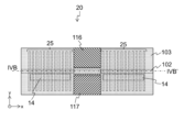
- FIG. 4A is a schematic top view showing the configuration of a semiconductor laser according to the second embodiment of the present invention.
- FIG. 4B is a schematic cross-sectional view taken along line IVB-IVB' showing the configuration of a semiconductor laser according to a second embodiment of the present invention.
- the x direction indicates the "length” direction
- the y direction indicates the “width” direction
- the z direction indicates the "height” direction, the "thickness” direction, or the vertical direction.
- a semiconductor laser 10 includes an active region 11 having an active layer 111, a front-stage waveguide region 12 having a front-stage waveguide connected to one end of the active layer 111, a rear-stage waveguide region 13 having a rear-stage waveguide connected to the other end of the active layer 111, a heater 14 disposed in the vicinity of the front-stage waveguide and the rear-stage waveguide, and a groove 15 disposed between the heater 14 and the active region 11.
- the semiconductor laser 10 comprises, in order, a substrate 101, a waveguide 102 made of a semiconductor, and an overclad 103 that covers the waveguide 102, and an active layer 111 in a portion of the waveguide 102.
- the semiconductor laser 10 has a lateral p-i-n diode formed in the active region 11. It has a layer structure consisting of an i (intrinsic) type semiconductor layer (lower part) 112, an active layer 111, and an i-type semiconductor layer (upper part) 113, a p-type semiconductor layer 114 disposed on one side wall of the layer structure, and an n-type semiconductor layer 115 disposed on the other side wall of the layer structure. Electrodes 116, 117 are provided on the surfaces of the p-type semiconductor layer 114 and the n-type semiconductor layer 115, respectively. This allows the semiconductor laser 10 to operate by injecting a current laterally into the active layer 111. When a signal current is injected into the active layer 111, the semiconductor laser outputs an optical modulation signal in response to the signal.
- the overclad 103 is a low refractive index medium such as SiO 2.
- the overclad 103 may be formed, for example, by surface activated bonding of the support substrate and the InP substrate, or may be formed by other methods.
- the active layer 111 is an InGaAsP-based multiple quantum well structure in the 1.31 ⁇ m wavelength band, with six quantum well layers.
- the active layer 111 is 150 nm thick.
- the i-type semiconductor layers 112 and 113 are each 50 nm thick and made of undoped InP.
- the p-type semiconductor layer 114 is, for example, Zn-doped (1 ⁇ 10 18 cm ⁇ 3 ) p-type InP
- the n-type semiconductor layer 115 is, for example, Si-doped (2 ⁇ 10 18 cm ⁇ 3 ) n-type InP.
- the length of the active layer 111 is 0.7 ⁇ m and the thickness is 0.32 ⁇ m.
- the thickness of the active layer 111, 0.32 ⁇ m, is approximately the upper limit value at which the light with a wavelength of 1.31 ⁇ m propagating through the active layer 111 becomes single mode in the thickness direction of the active layer 111.
- the waveguide 102 is made of undoped InP and has a layer thickness of 350 ⁇ m.
- a part of the waveguide 102 includes i-type semiconductor layers 112 and 113.
- the dimensions of the layer structure and the waveguide are not limited to these. Other dimensions are also acceptable.
- the thickness t of the active layer 111 When changing the operating wavelength or the material used for the active layer 111, in order for the active layer 111 to have a single mode in the thickness direction, the thickness t of the active layer 111 only needs to roughly satisfy the relationship in equation (1), where ⁇ is the operating wavelength, n core is the average refractive index of the active layer 111, and n clad is the refractive index of the second clad layer.
- the thickness t of the active layer (core layer) 111 is 0.364 ⁇ m or less.
- the heater 14 is disposed near the side of the waveguide 102 in the overclad 103, away from the active layer 111.
- the distance between the heater 14 and the active layer 111 depends on the thermal conductivity of the substrate 101.
- the distance between the heater 14 and the active layer 111 is about 1 to 10 ⁇ m, preferably about several ⁇ m.
- the distance between the heater 14 and the active layer 111 is about 10 to 100 ⁇ m, preferably about several tens of ⁇ m.
- the distance between the heater 14 and the waveguide 102 is, for example, about 1 to 10 ⁇ m, and preferably about 3 ⁇ m.
- the height of the heater 14 is approximately equal to the height of the waveguide 102. In other words, it is desirable that the position of the surface of the heater 14 is approximately equal to the position of the surface of the waveguide 102 in the vertical direction. This allows the heater and the waveguide to be integrated with approximately the same height when multilayer wiring is used in the semiconductor laser, thereby reducing the height of the stacked structure of the multilayer wiring.
- a groove 15 is formed in the overclad 103 between the active region 11 and the heater 14.
- the groove 15 is formed from the overclad 103 through the waveguide 102 to the inside of the substrate 101.
- the groove 15 is disposed to the side of the waveguide 102 at a distance approximately equal to the distance between the waveguide 102 and the heater 14.
- the position of the groove 15 is not limited thereto, and it need only be disposed so as to include a heat conduction path between the active region 11 and the heater 14.
- the length of the groove 15 is, for example, about 1 to 10 ⁇ m, and preferably about several ⁇ m.
- the width of the groove 15 is equal to or greater than the width of the heater 14, and preferably is longer.
- the depth of the groove 15 is, for example, about 200 to 300 ⁇ m.
- the groove 15 is filled with a gas, such as air, or may be filled with a material with low thermal conductivity.
- the heater 14 heats the front-stage waveguide and rear-stage waveguide to control the temperature. This controls the PPR frequency, increases the relaxation oscillation frequency, and expands the modulation bandwidth of the semiconductor laser.
- the groove 15 improves thermal isolation between the active layer 111 and the heater 14, making it possible to suppress a rise in temperature of the active layer 111.
- the insulation properties in the vicinity of the heater 14 are improved, making it possible to reduce the power consumption required to achieve a desired temperature rise.
- the positions of the heater 14 and the groove 15 are set at a distance that allows thermal conduction from the heater 14 to the waveguide 102 to the extent that the temperature of the waveguide 102 can be changed, and at a distance that allows thermal conduction from the heater 14 to the active layer 111 via the groove 15 to be suppressed.
- the support substrate 101 is made of Si or SiO 2 /Si.
- the support substrate 101 may be made of a heat dissipation substrate such as SiC, GaN, AlN, Al 2 O 3 , diamond, etc.
- the support substrate 101 is not limited to these, and may be made of other materials.
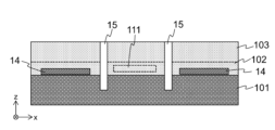
- the dependence of the temperature rise in the heater 14 and the active layer 111 when heated by the heater 14 on the depth of the groove 15 in the substrate (SiC) 101 was calculated using the finite element method.
- the structure used in the calculation is shown in Fig. 2.
- the heater 14 was made of platinum and had a resistance of 1.14 ⁇ .
- the active layer 111 was made of InP, the overcladding 103 was made of SiO2 , and the substrate 101 was made of SiC.
- the heater 14 and the active layer 111 were placed at the same height, the distance between the heater 14 and the active layer 111 was set to 30 ⁇ m, and a groove (length: 10 ⁇ m) 15 was placed in the middle.
- the groove 15 was assumed to be filled with air.
- the temperature rise in the heater 14 and active layer 111 when 700 mW of power is applied to the heater 14 was calculated by changing the depth of the groove 15 from 0 to 50 ⁇ m. At this time, the platinum 14 is heated, but the InP 111 is not heated. Other setting values are shown below.
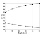
- Figure 3 shows the calculation results of the dependence of the temperature rise in the heater 14 and active layer 111 on the depth of the groove 15 in the substrate (SiC).
- the black circles and dotted line show the temperature rise in the heater 14, and the white circles and solid line show the temperature rise in the active layer (InP) 111.
- the amount of temperature rise in the heater 14 increases.
- the amount of temperature rise in the active layer (InP) 111 decreases. For example, when a 50 ⁇ m groove 15 is formed in SiC, the amount of temperature rise in the heater 14 increases by 28% and the amount of temperature rise in the active layer (InP) 111 decreases by 23% compared to when no groove is formed (when the groove depth is zero).
- the power consumption of the heater 14 to obtain the desired temperature increase can be reduced, and thermal isolation can be improved.
- the grooves improve thermal isolation between the active layer and the heater, making it possible to suppress temperature rise in the active layer.
- the insulation properties in the vicinity of the heater are improved, making it possible to reduce the power consumption required to achieve a desired temperature rise. This allows the semiconductor laser to operate over a wide frequency band.
- a groove 15_2 is provided near the waveguide in addition to the groove 15 arranged between the heater 14 and the active layer 111, but this is not limited to the example.
- a configuration may also be used in which only a groove 15 is provided between the heater 14 and the active layer 111.
- the number of heaters is not limited to two, but may be one, or three or more.
- the number of grooves is also not limited to two or four, but may be one, or three or more.
- the semiconductor laser 20 includes a substrate 101, an active layer 111, a front-stage waveguide, a rear-stage waveguide, an overclad 103, a heater 14, and a groove structure 25.
- the substrate 101, active layer 111, waveguide 102 (including the front-stage waveguide and rear-stage waveguide), overclad 103, and heater 14 have the same configuration as in the first embodiment.
- the groove structure 25 is composed of a number of periodically arranged grooves, and is arranged in the substrate 101 under the waveguides in the front-stage waveguide region and the rear-stage waveguide region and the overclad 103 on the sides of the waveguides.
- Each groove is filled with a gas, such as air.
- the grooves may be filled with a material with low thermal conductivity.
- the grooves improve thermal isolation between the active layer 111 and the heater 14, making it possible to suppress a rise in temperature of the active layer 111.
- the insulation properties in the vicinity of the heater 14 are improved, making it possible to reduce the power consumption required to achieve a desired temperature rise. This allows the semiconductor laser to operate over a wide frequency band.
- the groove structure 25 can be made to function as a diffraction grating.
- the front-stage waveguide and the rear-stage waveguide can be made to function as DBR waveguides.
- an example is shown in which an InGaAsP-based multiple quantum well structure in the 1.31 ⁇ m wavelength band is used for the active layer of the semiconductor laser, but this is not limited to this.
- Other wavelength bands such as the 1.55 ⁇ m wavelength band may also be used, and other materials such as AlGaAs, GaAs, and GaN may also be used.
- a semiconductor laser comprising a substrate, a waveguide, an overcladding covering the waveguide, an active layer disposed in a portion of the waveguide, a heater disposed near the side of the waveguide at a predetermined distance from the active layer, and a groove disposed between the active layer and the heater in a region including the substrate.
- Appendix 2 The semiconductor laser described in Appendix 1, in which the groove is disposed near the side of the waveguide between the active layer and the heater, from the surface of the overclad into the substrate.
- Appendix 3 The semiconductor laser according to appendix 1 or 2, further comprising a p-type semiconductor layer disposed on one sidewall of the active layer, an n-type semiconductor layer disposed on the other sidewall of the active layer, and electrodes disposed on the surfaces of the p-type semiconductor layer and the n-type semiconductor layer.
- Appendix 4 A semiconductor laser according to any one of appendices 1 to 3, in which the height of the heater and the height of the waveguide are approximately equal.
- Appendix 5 A semiconductor laser as described in appendix 1, appendix 3, or appendix 4, in which the grooves are periodically arranged below the heater within the substrate.
- the present invention relates to a semiconductor laser and can be applied to optical communication systems and optical transmitters.
Landscapes
- Physics & Mathematics (AREA)
- Condensed Matter Physics & Semiconductors (AREA)
- General Physics & Mathematics (AREA)
- Electromagnetism (AREA)
- Optics & Photonics (AREA)
- Semiconductor Lasers (AREA)
Priority Applications (2)
| Application Number | Priority Date | Filing Date | Title |
|---|---|---|---|
| PCT/JP2023/021689 WO2024257152A1 (ja) | 2023-06-12 | 2023-06-12 | 半導体レーザ |
| JP2025526903A JPWO2024257152A1 (https=) | 2023-06-12 | 2023-06-12 |
Applications Claiming Priority (1)
| Application Number | Priority Date | Filing Date | Title |
|---|---|---|---|
| PCT/JP2023/021689 WO2024257152A1 (ja) | 2023-06-12 | 2023-06-12 | 半導体レーザ |
Publications (1)
| Publication Number | Publication Date |
|---|---|
| WO2024257152A1 true WO2024257152A1 (ja) | 2024-12-19 |
Family
ID=93851447
Family Applications (1)
| Application Number | Title | Priority Date | Filing Date |
|---|---|---|---|
| PCT/JP2023/021689 Ceased WO2024257152A1 (ja) | 2023-06-12 | 2023-06-12 | 半導体レーザ |
Country Status (2)
| Country | Link |
|---|---|
| JP (1) | JPWO2024257152A1 (https=) |
| WO (1) | WO2024257152A1 (https=) |
Citations (7)
| Publication number | Priority date | Publication date | Assignee | Title |
|---|---|---|---|---|
| JPH07211984A (ja) * | 1994-01-18 | 1995-08-11 | Canon Inc | 光半導体デバイス及びその製造方法 |
| US20030086448A1 (en) * | 2001-11-08 | 2003-05-08 | Deacon David A.G. | Thermally wavelength tunable lasers |
| JP2004158636A (ja) * | 2002-11-06 | 2004-06-03 | Sumitomo Electric Ind Ltd | 半導体レーザ |
| JP2014017481A (ja) * | 2012-07-05 | 2014-01-30 | Jds Uniphase Corp | チューナブル・ブラッグ・グレーティング、およびそれを用いたチューナブル・レーザ・ダイオード |
| JP2015012176A (ja) * | 2013-06-28 | 2015-01-19 | 住友電工デバイス・イノベーション株式会社 | 光半導体装置及びその製造方法 |
| JP2019204904A (ja) * | 2018-05-24 | 2019-11-28 | 日本電信電話株式会社 | 半導体光モジュール |
| JP2021072299A (ja) * | 2019-10-29 | 2021-05-06 | 住友電気工業株式会社 | 半導体光素子 |
-
2023
- 2023-06-12 WO PCT/JP2023/021689 patent/WO2024257152A1/ja not_active Ceased
- 2023-06-12 JP JP2025526903A patent/JPWO2024257152A1/ja active Pending
Patent Citations (7)
| Publication number | Priority date | Publication date | Assignee | Title |
|---|---|---|---|---|
| JPH07211984A (ja) * | 1994-01-18 | 1995-08-11 | Canon Inc | 光半導体デバイス及びその製造方法 |
| US20030086448A1 (en) * | 2001-11-08 | 2003-05-08 | Deacon David A.G. | Thermally wavelength tunable lasers |
| JP2004158636A (ja) * | 2002-11-06 | 2004-06-03 | Sumitomo Electric Ind Ltd | 半導体レーザ |
| JP2014017481A (ja) * | 2012-07-05 | 2014-01-30 | Jds Uniphase Corp | チューナブル・ブラッグ・グレーティング、およびそれを用いたチューナブル・レーザ・ダイオード |
| JP2015012176A (ja) * | 2013-06-28 | 2015-01-19 | 住友電工デバイス・イノベーション株式会社 | 光半導体装置及びその製造方法 |
| JP2019204904A (ja) * | 2018-05-24 | 2019-11-28 | 日本電信電話株式会社 | 半導体光モジュール |
| JP2021072299A (ja) * | 2019-10-29 | 2021-05-06 | 住友電気工業株式会社 | 半導体光素子 |
Also Published As
| Publication number | Publication date |
|---|---|
| JPWO2024257152A1 (https=) | 2024-12-19 |
Similar Documents
| Publication | Publication Date | Title |
|---|---|---|
| Helkey et al. | High-performance photonic integrated circuits on silicon | |
| CN103597676B (zh) | 反射率调制光栅反射镜 | |
| CN110729630B (zh) | 一种采用铌酸锂材料制成的波长高速调谐的激光器 | |
| US6925098B2 (en) | Thermally wavelength tunable lasers | |
| US6853658B1 (en) | Optical logical circuits based on lasing semiconductor optical amplifiers | |
| JP6212754B2 (ja) | 光半導体装置及びその製造方法 | |
| JP2020517122A (ja) | 超周期構造回折格子および波長可変レーザ | |
| WO2021124440A1 (ja) | 光デバイス | |
| Guan et al. | Research on the asymmetric corrugation-pitch-modulated HR-AR DFB lasers with sampled gratings | |
| Ma et al. | Demonstration of a three-active-section DFB laser with photon-photon resonance and detuned loading effects to obtain enhanced bandwidth and maintained high output power | |
| JP2012033807A (ja) | 半導体レーザ | |
| JP6452198B2 (ja) | 半導体レーザ光源 | |
| Liu et al. | Single-mode surface-emitting DFB lasers with a large-area oxidized aperture based on the surface grating | |
| WO2024257152A1 (ja) | 半導体レーザ | |
| Liang et al. | A fully-integrated multi-λ hybrid DML transmitter | |
| US4639922A (en) | Single mode injection laser structure | |
| JP2019186446A (ja) | 半導体光素子 | |
| Peng et al. | A single-mode laser based on parity-time-symmetry structured vertical Bragg reflection waveguide | |
| JP7647887B2 (ja) | 半導体光デバイス | |
| JP7524973B2 (ja) | 光デバイス | |
| Zhang et al. | Enhancing Single-Mode Stability and Dynamic Characteristics in Complex-Coupled Grating WireLike Active-Region Membrane Distributed Reflector Lasers | |
| JP7294453B2 (ja) | 直接変調レーザ | |
| JPH0697604A (ja) | 分布反射型半導体レーザ | |
| JPH0697601A (ja) | 半導体光素子 | |
| JP7662035B2 (ja) | 半導体レーザ |
Legal Events
| Date | Code | Title | Description |
|---|---|---|---|
| 121 | Ep: the epo has been informed by wipo that ep was designated in this application |
Ref document number: 23941464 Country of ref document: EP Kind code of ref document: A1 |
|
| ENP | Entry into the national phase |
Ref document number: 2025526903 Country of ref document: JP Kind code of ref document: A |
|
| WWE | Wipo information: entry into national phase |
Ref document number: 2025526903 Country of ref document: JP |
|
| NENP | Non-entry into the national phase |
Ref country code: DE |