WO2024253100A1 - ゲート駆動装置 - Google Patents
ゲート駆動装置 Download PDFInfo
- Publication number
- WO2024253100A1 WO2024253100A1 PCT/JP2024/020414 JP2024020414W WO2024253100A1 WO 2024253100 A1 WO2024253100 A1 WO 2024253100A1 JP 2024020414 W JP2024020414 W JP 2024020414W WO 2024253100 A1 WO2024253100 A1 WO 2024253100A1
- Authority
- WO
- WIPO (PCT)
- Prior art keywords
- gate
- path
- current
- wiring
- switching element
- Prior art date
- Legal status (The legal status is an assumption and is not a legal conclusion. Google has not performed a legal analysis and makes no representation as to the accuracy of the status listed.)
- Ceased
Links
Images


Classifications
-
- H—ELECTRICITY
- H02—GENERATION; CONVERSION OR DISTRIBUTION OF ELECTRIC POWER
- H02M—APPARATUS FOR CONVERSION BETWEEN AC AND AC, BETWEEN AC AND DC, OR BETWEEN DC AND DC, AND FOR USE WITH MAINS OR SIMILAR POWER SUPPLY SYSTEMS; CONVERSION OF DC OR AC INPUT POWER INTO SURGE OUTPUT POWER; CONTROL OR REGULATION THEREOF
- H02M1/00—Details of apparatus for conversion
- H02M1/08—Circuits specially adapted for the generation of control voltages for semiconductor devices incorporated in static converters
-
- H—ELECTRICITY
- H03—ELECTRONIC CIRCUITRY
- H03K—PULSE TECHNIQUE
- H03K17/00—Electronic switching or gating, i.e. not by contact-making and –breaking
- H03K17/16—Modifications for eliminating interference voltages or currents
-
- H—ELECTRICITY
- H03—ELECTRONIC CIRCUITRY
- H03K—PULSE TECHNIQUE
- H03K17/00—Electronic switching or gating, i.e. not by contact-making and –breaking
- H03K17/51—Electronic switching or gating, i.e. not by contact-making and –breaking characterised by the components used
- H03K17/56—Electronic switching or gating, i.e. not by contact-making and –breaking characterised by the components used by the use, as active elements, of semiconductor devices
- H03K17/687—Electronic switching or gating, i.e. not by contact-making and –breaking characterised by the components used by the use, as active elements, of semiconductor devices the devices being field-effect transistors
Definitions
- the present invention relates to a gate drive device for a semiconductor switching element.
- Power semiconductor elements are used in various devices, for example, as switching elements in inverter circuits of power conversion devices.
- switching loss occurs when the switching operation is turned on and off.
- a multi-stage gate drive circuit that switches gate resistors is known as a configuration that can adjust the switching speed (see Patent Document 1).
- a gate driver is a gate driver that applies a voltage to a gate terminal of a semiconductor switching element, and includes a first path connected to the gate terminal and having a first gate resistor, a second path connected to the gate terminal in parallel with the first path and having a second gate resistor, and an active gate control unit that controls the gate current when switching the switching state of the semiconductor switching element so that the gate current flows through both the first path and the second path and then flows only through the first path, and the inductance component of the second path is set to a value larger than the inductance component of the first path.
- the present invention makes it possible to increase the speed and reduce loss of the switching operation of semiconductor switching elements.
- FIG. 1 is a diagram illustrating an example of a power conversion device.
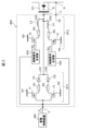
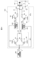
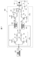
- FIG. 2 is a diagram showing a circuit configuration of the gate driver.
- FIG. 3 is a diagram showing an example of the waveforms of each signal when the transistor is turned on.
- FIG. 4 is a diagram showing a comparative example of a gate driving device.
- FIG. 5 is a diagram showing an example of the waveforms of the signals at the time of turn-off.
- FIG. 6 is a diagram showing a first modified example.
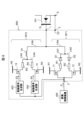
- FIG. 7 is a diagram illustrating the second modified example.
- FIG. 8 is a diagram showing a second embodiment.
- (First embodiment) 1 is a diagram illustrating an example of a power conversion device.
- a power conversion device 200 mounted on a vehicle 1000 will be described as an example.
- the power conversion device 200 drives an electric motor 300 mounted on the vehicle 1000.
- the vehicle 1000 is provided with a power storage device 100, and the power conversion device 200 converts DC power supplied from the power storage device 100 into AC power to drive the electric motor 300.
- the electric motor 300 is, for example, a traction motor for rotating wheels.
- the electric motor 300 has three-phase coils that are connected in a predetermined pattern.
- the connection pattern is not limited to the Y pattern shown in FIG. 1, and other connection patterns such as a delta pattern may also be used.
- the electric motor 300 is driven to rotate by applying a predetermined current pattern from the power conversion device 200 to the three-phase coils.
- the energy storage device 100 has a positive terminal 100a and a negative terminal 100b.
- the power conversion device 200 has a positive bus line 201p, a negative bus line 201n, a smoothing capacitor 110, and a three-phase switching arm 500 (U, V, W).
- the positive bus line 201p is connected to the positive terminal 100a of the energy storage device 100.
- the negative bus line 201n is connected to the negative terminal 100b of the energy storage device 100. Both ends of the smoothing capacitor 110 and the three-phase switching arm 500 (U, V, W) are connected to the positive bus line 201p and the negative bus line 201n.
- Each of the three-phase switching arms 500 (U, V, W) is provided with an upper arm switching element 101 and a lower arm switching element 101.
- the switching elements 101 are, for example, power switching elements, and for example, IGBTs or MOSFETs are used.
- Each switching element 101 has a freewheeling diode (or body diode) 102 connected in parallel.
- the upper arm switching element 101 and the lower arm switching element 101 are connected in series.
- the connection point between the upper arm switching element 101 and the lower arm switching element 101 is connected to one end of the coil of the corresponding phase of the electric motor 300.
- one switching element 101 is provided in each of the upper and lower arms, but a configuration in which multiple switching elements 101 are used in parallel may also be used.
- the power conversion device 200 includes a conversion control device 400 that controls the gate drive device 600.
- the conversion control device 400 outputs a control command P to each gate drive device 600 and controls each switching element 101 individually.
- the control command P is a pulse signal with a predetermined pulse width, and the conversion control device 400 PWM controls the switching elements 101.
- This control command P controls the switching elements 101 of the same phase to be alternately turned on/off within a range where they are not turned on simultaneously. As a result, the DC power from the storage device 100 is converted to AC power, and the electric motor 300 is driven to rotate.
- the power conversion device 200 constituting an inverter as shown in FIG. 1 will be described as an example, but the present invention is not limited to this and can also be applied to DC/DC converters, AC/AC converters, AC/DC inverters, etc.
- FIG. 2 shows the circuit configuration of the switching element 101 for the lower arm of the U phase shown in FIG. 1, and the gate driver 600 provided for that switching element 101.
- the upper arm of the U phase and the upper and lower arms of the other phases have a similar configuration.
- the switching element used is a MOSFET.
- the output section 1 of the gate driver 600 is connected to the gate terminal G of the switching element 101, and the reference potential 2 is connected to the source terminal S of the switching element 101.
- the input section 3 of the gate driver 600 is connected to the conversion control device 400.
- the control command P input from the conversion control device 400 to the gate driver 600 is input to the gates of the MOSFETs 11 and 12, and is also input to the control signal generating sections 403 and 404.
- the gate driver 600 has two paths RT1 and RT2 connected to the gate terminal G of the switching element 101.
- the control circuits of the conversion control device 400 and the control signal generating sections 403 and 404 have, for example, a CPU, RAM, ROM, communication circuits, etc., internally, although not shown.
- the conversion control device 400 and the control signal generating sections 403 and 404 may also be configured as a single control device.
- the first path RT1 includes wiring LN1 and wiring LN2.
- Wiring LN1 has a positive power supply N1, an on-side MOSFET 11, an on-side gate resistor R1, and a diode D1.
- the source of MOSFET 11 is connected to the positive power supply N1, and the drain is connected to one end of the gate resistor R1.
- the other end of the gate resistor R1 is connected to the anode of the diode D1.
- the cathode of the diode D1 is connected to the gate terminal G.
- Line LN2 has a negative power supply N2, an off-side MOSFET 12, an off-side gate resistor R2, and a diode D2.
- the source of MOSFET 12 is connected to the negative power supply N2, and the drain is connected to one end of the gate resistor R2.
- the other end of the gate resistor R2 is connected to the cathode of diode D2.
- the anode of diode D2 is connected to the gate terminal G.
- the configuration may omit diode D1 on line LN1 or diode D2 on line LN2. In this case, one end of the gate resistors R1 and R2 is connected to the gate terminal G.
- the second path RT2 includes wiring LN3 and wiring LN4.
- Wiring LN3 has a positive power supply N3, a MOSFET 13 for voltage boosting, a gate resistor R3, and an inductance component L3.
- the source of MOSFET 13 is connected to the positive power supply N3, and the drain is connected to one end of the gate resistor R3.
- the other end of the gate resistor R3 is connected to the gate terminal G via the inductance component L3.
- Line LN4 has a negative power supply N4, a voltage-pulling MOSFET 14, a gate resistor R4, and an inductance component L4.
- the source of MOSFET 14 is connected to the negative power supply N4, and the drain is connected to one end of the gate resistor R4.
- the other end of the gate resistor R4 is connected to the gate terminal G via the inductance component L4.
- the input section of MOSFET 13 is connected to a control signal generating section 403, and a control signal S3 is input from the control signal generating section 403.
- the input section of MOSFET 14 is connected to a control signal generating section 404, and a control signal S4 is input from the control signal generating section 404.
- the control signal generating units 403 and 404 generate the control signals S3 and S4 based on the control command P input from the conversion control device 400. Note that the configuration may also be such that the state of the switching element 101 is sensed and the state signal J is input to the control signal generating units 403 and 404. In that case, the control signal generating units 403 and 404 generate the control signals S3 and S4 based on the control command P and the state signal J.
- the inductance component of the wiring LN3 is set to be larger than the inductance component of the wiring LN1 by the inductance component L3.
- the inductance component of the wiring LN4 is set to be larger than the inductance component of the wiring LN2 by the inductance component L4.
- the setting range of the inductance components L3 and L4 is set to be, for example, about 100 nH to 2000 nH.
- the positive power supply N1 and the positive power supply N3 are basically set to the same potential, but may be set to different potentials.
- the potential of the positive power supply N1 may be set to be higher than the potential of the positive power supply N3 by the forward voltage of diode D1.
- BJTs Bipolar Junction Transistors
- the inductance components L3 and L4 may be placed on the wiring LN3 and LN4.
- the inductors may be placed between MOSFET 13 and gate resistor R3, and between MOSFET 14 and gate resistor R4, or may be distributed over the wiring LN3 and LN4.
- the magnitude of the inductance components may be adjusted by adjusting the wiring length and width of the wiring LN1 to LN4.
- the magnitude of the inductance components may be adjusted by using lead-type gate resistors R3 and R4 or MOSFETs 13 and 14 and changing the length of the lead wires.
- Other methods for adjusting the inductance component include making the wiring spiral or zigzag, or locally narrowing parts of the wiring. Furthermore, by implementing ferrite beads, the desired inductance component can be obtained even with short lead wires, making it possible to miniaturize the power supply circuit.
- FIG. 3 is a diagram showing an example of the waveforms of each signal when the switching element 101 is turned on.
- Waveform (A) shows a control command P from the conversion control device 400.
- Waveform (B) shows a control signal S3 from the control signal generating unit 403.
- Waveform (C) shows the gate current Ig of the switching element 101.
- Waveform (D) shows the gate voltage Vgs of the switching element 101.
- the thin solid line and dashed line of waveform (E) show the drain-source main voltage (hereinafter referred to as drain-source voltage) Vds of the switching element 101, and the thick solid line and dashed line show the drain current Ids.
- the conventional case refers to a gate driver 610 having a configuration such as that shown in the comparative example of FIG. 4.
- the gate driver 610 is obtained by omitting the inductance components L3 and L4 of the second path RT2 and the diodes D1 and D2 of the first path RT1 from the gate driver 600 shown in FIG. 2.
- a control command P (ON) for turning on the gate of the switching element 101 is input from the conversion control device 400 to the gate drive device 600.
- the control command P (ON) is input to the gate drive device 600, the MOSFET 11 is turned on.
- a control signal S3 (pulse command) for turning on the MOSFET 13 is input from the control signal generation unit 403 to the MOSFET 13. Since the MOSFET 13 is a P-type MOSFET, inversion is required, but here the pulse command before inversion is shown.
- the waveform of the control signal S3 is expressed in the same waveform as the control signal S4 for the N-type MOSFET 14 with respect to the on/off of the control command P.
- the rising edge of the control signal S3 should be set so as not to be delayed from the control command P, and preferably should be synchronized. It may also rise before the control command P.
- the gate current Ig of the switching element 101 begins to rise as shown in waveform (C).
- the gate current Ig is the sum of the gate currents on the first and second paths RT1 and RT2.
- the gate voltage Vgs begins to rise as shown in waveform (D).
- the gate current begins to flow simultaneously on the first path RT1 and the second path RT2 as shown by the solid and dashed lines.
- the gate current Ig rises more slowly than in the comparative example (dashed line), and the gate voltage Vgs also rises accordingly more slowly.
- the gate current Ig is larger than in this embodiment, so the gate capacitance is charged faster. Therefore, in the comparative example, the gate voltage Vgs reaches the gate threshold voltage Vth earlier.
- the gate voltage Vgs reaches the gate threshold voltage Vth at time t1
- the drain-source voltage Vds of the switching element 101 begins to decrease as shown by the thin dashed line in the waveform (E)
- the drain current Ids begins to increase as shown by the thick dashed line in the waveform (E).
- the gate capacitance is charged slower than in the comparative example, so the gate voltage Vgs reaches the gate threshold voltage Vth at time t2 (>t1).
- the drain-source voltage Vds begins to decrease, and the drain current Ids begins to increase.
- loss in the semiconductor switching element occurs from the timing when the drain current Ids begins to increase.
- the gate current Ig is larger than in this embodiment, so the gate current Ig reaches its peak value sooner.
- the gate current Ig is determined by dividing the difference between the gate voltage Vgs and the positive power supply of the switching element 101 by the gate resistance value.
- the gate voltage Vgs rises faster than in this embodiment, as shown in waveform (D), so the difference between the gate voltage Vgs and the positive power supply also decreases sooner. Therefore, the gate current Ig after reaching its peak value in the comparative example is attenuated more strongly than in the embodiment.
- the rate at which the drain-source voltage Vds decreases and the rate at which the drain current Ids rises are proportional to the gate current Ig, so the speed at which the drain-source voltage Vds and the drain current Ids change in the comparative example is slower than in the first embodiment.
- the charging speed is reduced by switching the MOSFET 13 from the on state to the off state, stopping the flow of the gate current of the second path RT2 and allowing the gate current to flow only through the first path RT1, thereby reducing the gate current.
- This switching must be completed before a surge of the drain current Ids occurs. Therefore, it is necessary to turn off the control signal S3 within the period from the rising edge of the drain current Ids to the time t3 at which the drain current Ids reaches its maximum.
- the main part of the time that the control signal S3 is in the on state is the charging period until the gate voltage Vgs reaches the gate threshold voltage Vth.
- the control signal S3 in the comparative example since the period until the gate voltage Vgs reaches the gate threshold voltage Vth is short, the control signal S3 must be turned off at an earlier timing than in the first embodiment, as shown in waveform (B). Therefore, the control signal S3 in the comparative example has a shorter pulse width than the control signal S3 in the first embodiment. That is, in the first embodiment, the charging time until the gate threshold voltage is longer, and the gate drive speed can be switched with a control signal S3 having a longer pulse than in the past.
- the timing to end the control signal S3 is determined, for example, based on the control command P.
- the timing to end the control signal S3 may also be determined based on the state signal J of the switching element 101 described above.
- the state signal J may be, for example, a rising edge of the rate of change of any of the gate current Ig, gate voltage Vgs, drain current Ids, and drain-source main voltage Vds, or a falling edge of the rate of change of the drain-source voltage Vds or drain current Ids.
- the gate current Ig rises quickly and immediately decays.
- inductance components L3 and L4 are provided, so the decay of the gate current Ig during switching can be weakened as shown by the solid line. As a result, the switching speed can be improved.
- the loss power shown in waveform (F) is expressed as the product of the drain-source voltage Vds and the drain current Ids.
- the period during which losses occur is shortened due to the improved switching speed, so the amount of loss, which is the time integral of the loss power, is smaller than in the comparative example shown by the dashed line. In other words, the loss at turn-on can be reduced.
- FIG. 5 is a diagram showing an example of the waveforms of each signal when the switching element 101 is turned off.
- Waveform (A) shows a control command P from the conversion control device 400.
- Waveform (B) shows a control signal S4 from the control signal generating unit 404.
- Waveform (C) shows the gate current Ig of the switching element 101.
- Waveform (D) shows the gate voltage Vgs of the switching element 101.
- the thin solid line and dashed line of waveform (E) show the drain-source voltage Vds of the switching element 101, and the thick solid line and dashed line show the drain current Ids.
- a control command P (OFF) for gating off (OFF) the switching element 101 is input from the conversion control device 400 to the gate drive device 600.
- the MOSFET 12 turns on.
- a control signal S4 (pulse command) for turning on the MOSFET 14 is input from the control signal generation unit 404 to the MOSFET 14.
- the rising edge of the control signal S4 should be set so as not to lag behind the falling edge of the control command P, and preferably should be synchronized. It may also rise before the falling edge of the control command P.
- the gate current Ig starts to flow, discharging the gate capacitance of the switching element 101, as shown in waveform (C).
- the gate current Ig is the sum of the gate currents on the first and second paths RT1 and RT2. As the gate current Ig starts to flow, the gate voltage Vgs starts to decrease. In both the first embodiment and the comparative example, the gate current starts to flow simultaneously on the first and second paths RT1 and RT2, as shown by the solid and dashed lines.
- the gate current (discharge current) Ig is larger than in this embodiment, so the gate capacitance is discharged faster. Therefore, as shown in waveform (D), the gate voltage Vgs in the comparative example reaches the gate's Miller Plateau first. When the gate voltage Vgs in the comparative example shown by the dashed line reaches the gate's Miller Plateau at time t1, the drain-source voltage Vds begins to rise, as shown by the thin dashed line in waveform (E).
- the gate voltage Vgs reaches the gate Miller plateau at time t2 (> t1).
- the drain-source voltage Vds starts to rise at time t2, and as shown in the waveform (F), a loss occurs in the switching element 101 from this timing.
- the gate current Ig is larger than in this embodiment, so as shown in waveform (C), the gate current Ig reaches its peak on the discharge side earlier than in this embodiment.
- the gate current Ig is determined by dividing the difference between the gate voltage Vgs and the negative power supply of the switching element 101 by the gate resistance value.
- the gate voltage Vgs decreases faster than in this embodiment, so the difference between the gate voltage Vgs and the negative power supply also decreases more quickly. Therefore, the gate current Ig after reaching its peak value in the comparative example is attenuated more strongly than in the embodiment. Since the rate of rise of the drain-source voltage Vds is proportional to the magnitude of the gate current Ig, the rate of rise of the drain-source voltage Vds in the comparative example is slower than in this embodiment.
- the timing for switching from high-speed mode to low-speed mode must be completed before the drain-source voltage Vds surges.
- the control signal S4 must be turned off within the period from the rising edge of the drain-source voltage Vds to time t3, when the drain-source voltage Vds reaches its maximum.
- the main part of the time until the control signal S4 is turned off is the discharge period until the gate voltage Vgs reaches the Miller plateau.
- the discharge period until the gate voltage Vgs reaches the Miller plateau is shorter in the comparative example than in the first embodiment. Therefore, in the comparative example, the control signal S4 must be turned off at an earlier timing than in the first embodiment. As a result, the pulse width of the control signal S4 (dashed line) in the comparative example is shorter than the control signal S4 (solid line) in the first embodiment. That is, as in the case of the control signal S3, the first embodiment allows control with a longer pulse width than the comparative example, making design easier.
- the timing to end the control signal S4 is determined, for example, based on the control command P.
- the timing to end the control signal S3 may also be determined based on the state signal J of the switching element 101 described above.
- the state signal J may be, for example, a falling edge in the rate of change of any of the gate current Ig, gate voltage Vgs, drain current Ids, and drain-source main voltage Vds, or a rising edge in the rate of change of the drain-source voltage Vds or drain current Ids.
- the gate current Ig rises quickly and then decays immediately.
- inductance components L3 and L4 are provided, it is possible to weaken the decay of the gate current Ig during switching, as shown by the solid line. As a result, the switching speed can be improved.
- diodes D1 and D2 that limit the direction of gate current flow and preventing backflow into the first path RT1
- (Variation 1) 6 is a diagram showing a first modification of the first embodiment described above.
- the inductance components L3 and L4 shown in FIG. 2 of the first embodiment are made common by an inductance component Lb.
- the wiring LN3 and the wiring LN4 are connected to the gate terminal G via a wiring LNb having an inductance component Lb.
- the wiring LN1 and the wiring LN2 are connected to the gate terminal G via a wiring LNa.
- a common inductance component Lb is added to each of the wirings LN3 and LN4.
- the magnitude of the inductance component Lb is set so that the total inductance component of the wirings LN3 and LNb, and the total inductance component of the wirings LN4 and LNb are both greater than the inductance component of the first path RT1.
- (Variation 2) 7 is a diagram illustrating a second modified example of the first embodiment described above.
- a diode D3 is further provided between the positive power supply N3 and the gate terminal G in addition to the configuration of FIG. 2.
- the operation at the time of turn-on and turn-off is the same as that of the first embodiment described above.
- the excess charge at the gate of the switching element 101 returns to the positive power supply N3. This makes it possible to prevent the gate from being overcharged.
- FIG. 8 is a diagram showing a second embodiment of the present invention.
- the source of the MOSFET 13, which is a switching element is connected to the positive power supply N3, but in Fig. 8, the source of the MOSFET 13 is connected to the drain of the MOSFET 11.
- the source of the MOSFET 14 is connected to the drain of the MOSFET 12.
- the MOSFETs 13 and 14 provided on the wirings LN3 and LN4 are shown as switches. These switches may be BJTs (Bipolar Junction Transistors) instead of MOSFETs.
- the symbols RT1 and RT2 indicating the first and second paths are omitted.
- the current (gate current) flowing through wiring LN3 of the second path is controlled by both MOSFETs 11 and 13, and the current flowing through wiring LN4 is controlled by both MOSFETs 12 and 14. That is, a current flows through wiring LN3 only when both MOSFETs 11 and 13 are on. In the case of wiring LN4, a current flows only when both MOSFETs 12 and 14 are on.
- MOSFET 13 is turned on before or at the same time as MOSFET 11, gate current can automatically and simultaneously begin to flow through wiring LN1 and wiring LN3.
- the same is true for wiring LN2 and LN4. Therefore, by setting the on-timing of MOSFETs 13 and 14 earlier than the on-timing of MOSFETs 11 and 12, the pulse width of the control signals S3 and S4 for MOSFETs 13 and 14 can be lengthened. This improves the controllability of the gate drive device 600 and makes it possible to implement slow-response control elements on wiring LN3 and LN4 on the second path.
- the gate driver 600 applies a voltage to the gate terminal G of the switching element 101.
- the gate driver 600 includes a first path RT1 connected to the gate terminal G and having gate resistors R1 and R2, a second path RT2 connected to the gate terminal G in parallel with the first path RT1 and having gate resistors R3 and R4, and control signal generators 403 and 404 (active gate controllers) that control the gate current when switching the switching state of the switching element 101 so that the gate current flows only through path RT1 after flowing through both paths RT1 and RT2.
- the inductance component of path RT2 is set to a value larger than the inductance component of path RT1.
- the inductance component of path RT2 is set to be larger than path RT1 by inductance components L3 and L4.
- the inductance component of path RT2 is set to be larger than that of path RT1, the attenuation of the gate current during switching can be weakened. As a result, the switching speed can be improved and the loss during switching can be reduced. Furthermore, even if the switching element 101 is a power element with a large built-in resistance, it can be driven at high speed.
- the second path RT2 is provided with a charging line LN3 and a discharging line LN4, but a configuration in which only one of them is provided may also be used.
- the path RT1 further includes diodes D1 and D2 that limit the direction of the gate current. This can prevent losses in the path RT1 due to the backflow of the gate current, and can suppress heat generation in the gate substrate.
- the current flowing through the path RT2 can be efficiently used to charge and discharge the gate capacitance, improving the gate charge and discharge speed.
- the inductance component of path RT2 may be configured with an inductor or ferrite beads.
- an inductor By adjusting the inductance components L3 and L4 using an inductor, it is possible to easily and accurately adjust the inductance components L3 and L4.
- the desired inductance component can be obtained even with short wiring, and the power supply circuit can be made smaller.
- At least a portion of the inductance components L3 and L4 in the path RT2 may be set by the wiring length of the path RT2 or the lead length of the components in the path RT2. This makes it easier to design the layout on the board.
- MOSFETs 11 and 12 are provided on path RT1 and allow and block the passage of gate current
- MOSFETs 13 and 14 are provided on path RT2 and allow and block the passage of gate current.
- the control signal generating units 403 and 404 active gate control units allow the passage of current through MOSFETs 13 and 14 before or at the same time as allowing the passage of current through MOSFETs 11 and 12.
- MOSFETs 11 and 12 are provided on path RT1 to allow and block the passage of gate current
- MOSFETs 13 and 14 are provided on path RT2 to allow and block the passage of gate current.
- the control signal generation units 403 and 404 active gate control units block the passage of current through MOSFETs 13 and 14 before the timing of the surge peak of the switching current (drain current Ids) or switching voltage (drain-source voltage Vds) of the switching element 101.
- the gate current flowing through the gate of switching element 101 is reduced. This reduces the switching speed, making it possible to suppress surges in the drain current Ids or drain-source voltage Vds.
- MOSFETs 11, 12 are provided on the path RT1 on the opposite side of the gate terminal G across the gate resistors R1, R2, and allow and block the passage of the gate current
- MOSFETs 13, 14 are provided on the path RT2 (wiring LN3, LN4) and allow and block the passage of the gate current
- one end of the path RT2 (wiring LN3, LN4) is connected between the gate resistors R1, R2 and the MOSFETs 11, 12, and the other end of the path RT2 is connected to the gate terminal G
- the conversion control device 400 and the control signal generation units 403, 404 active gate control units
- the path RT2 includes a wiring LN3 having a gate resistor R3 for charging the gate capacitance of the switching element 101, a wiring LN4 having a gate resistor R4 for discharging the gate capacitance of the switching element 101, and a wiring LNb having one end connected to the wiring LN3 and the wiring LN4 and the other end connected to the gate terminal G, and the inductance component of the wiring consisting of the wiring LN3 and the wiring LNb and the inductance component of the wiring consisting of the wiring LN4 and the wiring LNb are each set to a value larger than the inductance component of the path RT1.
- the inductance component of the second path is shared, which reduces the number of components (inductors) and simplifies the circuit.
- the path RT2 includes a wiring LN3 that connects a positive power supply N3 (gate charge power supply) for charging the gate capacitance of the switching element 101 to the gate terminal G, and a diode D3 that is provided between the positive power supply N3 and the gate terminal G, with the cathode connected to the positive power supply N3 and the anode connected to the gate terminal G.
- N3 gate charge power supply
- the excess gate charge can be fed back to the positive power supply N3. This makes it possible to prevent the gate from being overcharged.
Landscapes
- Engineering & Computer Science (AREA)
- Power Engineering (AREA)
- Power Conversion In General (AREA)
- Electronic Switches (AREA)
Abstract
半導体スイッチング素子(101)のゲート端子(G)に電圧を印加するゲート駆動装置(600)は、前記ゲート端子に接続され、第1ゲート抵抗(R1、R2)を有する第1経路(RT1)と、前記第1経路と並列に前記ゲート端子に接続され、第2ゲート抵抗(R3、R4)を有する第2経路(RT2)と、前記半導体スイッチング素子のスイッチング状態を切り替える際のゲート電流が、前記第1経路および前記第2経路の両方に流れた後に、前記第1経路のみに流れるように制御するアクティブゲート制御部(403、404)と、を備え、前記第2経路のインダクタンス成分(L3、L4)は前記第1経路のインダクタンス成分よりも大きな値に設定されている。
Description
本発明は、半導体スイッチング素子のゲート駆動装置に関する。
パワー半導体素子は種々の装置に用いられており、例えば、電力変換装置のインバータ回路のスイッチング素子として用いられている。このようなパワー半導体素子においては、スイッチング動作のターンオンおよびターンオフに伴ってスイッチング損失が発生する。そのため、電力変換装置では、小型化や高出力密度化のために、パワー半導体素子の低損失化が重要となる。例えば、スイッチング速度の調整が可能な構成として、ゲート抵抗の切り替えによる多段式ゲート駆動回路が知られている(特許文献1参照)。
しかしながら、特許文献1に記載の構成では、スイッチング動作中のゲート電流の減衰が大きいため、高速化による低損失駆動が難しい。
本発明の態様によるゲート駆動装置は、半導体スイッチング素子のゲート端子に電圧を印加するゲート駆動装置であって、前記ゲート端子に接続され、第1ゲート抵抗を有する第1経路と、前記第1経路と並列に前記ゲート端子に接続され、第2ゲート抵抗を有する第2経路と、前記半導体スイッチング素子のスイッチング状態を切り替える際のゲート電流が、前記第1経路および前記第2経路の両方に流れた後に、前記第1経路のみに流れるように制御するアクティブゲート制御部と、を備え、前記第2経路のインダクタンス成分は前記第1経路のインダクタンス成分よりも大きな値に設定されている。
本発明によれば、半導体スイッチング素子のスイッチング動作の高速化および低損失化を図ることができる。
以下、図を参照して本発明を実施するための形態について説明する。以下の記載および図面は、本発明を説明するための例示であって、説明の明確化のため、適宜、省略および簡略化がなされている。また、以下の説明では、同一または類似の要素および処理には同一の符号を付し、重複説明を省略する場合がある。なお、以下に記載する内容はあくまでも本発明の実施の形態の一例を示すものであって、本発明は下記の実施の形態に限定されるものではなく、他の種々の形態でも実施する事が可能である。
(第1の実施形態)
図1は、電力変換装置の一例を示す図である。第1の実施形態では、車両1000に搭載された電力変換装置200を例に説明する。電力変換装置200は、車両1000に搭載された電動モータ300を駆動する。車両1000には蓄電装置100が設けられ、電力変換装置200は蓄電装置100から供給される直流電力を交流電力に変換し、電動モータ300を駆動する。
図1は、電力変換装置の一例を示す図である。第1の実施形態では、車両1000に搭載された電力変換装置200を例に説明する。電力変換装置200は、車両1000に搭載された電動モータ300を駆動する。車両1000には蓄電装置100が設けられ、電力変換装置200は蓄電装置100から供給される直流電力を交流電力に変換し、電動モータ300を駆動する。
電動モータ300は、例えば、車輪を回転させるための走行用モータである。電動モータ300は、所定のパターンで結線される3相コイルを有する。結線パターンとしては、図1に示すY字パターンに限られず、デルタパターンのような他の結線パターンでも良い。電力変換装置200から所定の通電パターンを3相コイルに印加することにより、電動モータ300が回転駆動される。
蓄電装置100は、正極端子100aおよび負極端子100bを有する。電力変換装置200は、正極バス線201p、負極バス線201n、平滑コンデンサ110および三相スイッチングアーム500(U,V,W)を有する。正極バス線201pは、蓄電装置100の正極端子100aに接続される。負極バス線201nは、蓄電装置100の負極端子100bに接続される。平滑コンデンサ110および三相スイッチングアーム500(U,V,W)の両端は、正極バス線201pと負極バス線201nとに接続される。
三相スイッチングアーム500(U,V,W)のそれぞれには、上アームのスイッチング素子101と下アームのスイッチング素子101が設けられている。スイッチング素子101は、例えばパワースイッチング素子であり、例えば、IGBTあるいはMOSFET等が用いられる。各スイッチング素子101は、並列接続された還流ダイオード(または、ボディーダイオード)102を有する。上アームのスイッチング素子101と下アームのスイッチング素子101とは直列に接続されている。上アームのスイッチング素子101と下アームのスイッチング素子101との接続点は、電動モータ300の対応する相のコイルの一端に接続されている。なお、図1に示す例では、各上下アームに1つのスイッチング素子101が設けられているが、複数のスイッチング素子101を並列使用する構成であっても良い。
電力変換装置200は、ゲート駆動装置600を制御する変換制御装置400を備える。変換制御装置400は、ゲート駆動装置600毎に制御指令Pを出力し、各スイッチング素子101を個別に制御する。制御指令Pは所定のパルス幅を有するパルス信号であり、変換制御装置400はスイッチング素子101をPWM制御する。この制御指令Pによって、同一の相のスイッチング素子101は、同時にオンにならない範囲で交互にオン/オフ制御される。その結果、蓄電装置100からの直流電力が交流電力に変換されて電動モータ300が回転駆動される。
なお、本実施形態では、図1に示すようなインバータを構成する電力変換装置200を例に説明するが、本発明は、これに限られず、DC/DCコンバータ、AC/ACコンバータ、AC/DCインバータ等にも適用することができる。
図2は、図1に示したU相の下アームに係るスイッチング素子101と、そのスイッチング素子101に対して設けられたゲート駆動装置600の回路構成を示したものである。なお、図示は省略するが、U相の上アームおよび他の相(V,W相)の上下アームについても同様の構成である。以下の説明では、用いられるスイッチング素子がMOSFETの場合を例に説明する。
ゲート駆動装置600の出力部1はスイッチング素子101のゲート端子Gに接続され、基準電位2はスイッチング素子101のソース端子Sと接続される。ゲート駆動装置600の入力部3は、変換制御装置400と接続される。変換制御装置400からゲート駆動装置600に入力された制御指令Pは、MOSFET11,12のゲートに入力されると共に、制御信号生成部403,404にも入力される。ゲート駆動装置600は、スイッチング素子101のゲート端子Gに接続される2つの経路RT1および経路RT2を有する。変換制御装置400、制御信号生成部403,404は、例えば、図示は省略するが、制御回路は内部にCPU、RAM、ROM、通信回路等を有している。また、変換制御装置400および制御信号生成部403,404を、一つの制御装置で構成するようにしても良い。
第1の経路RT1は、配線LN1と配線LN2とを備える。配線LN1は、正側電源N1、オン側のMOSFET11、オン側のゲート抵抗R1およびダイオードD1を有する。MOSFET11は、ソースが正側電源N1に接続され、ドレインがゲート抵抗R1の一端に接続される。ゲート抵抗R1の他端はダイオードD1のアノードに接続される。ダイオードD1のカソードはゲート端子Gに接続される。
配線LN2は、負側電源N2、オフ側のMOSFET12、オフ側のゲート抵抗R2およびダイオードD2を有する。MOSFET12は、ソースが負側電源N2に接続され、ドレインがゲート抵抗R2の一端に接続される。ゲート抵抗R2の他端はダイオードD2のカソードに接続される。ダイオードD2のアノードはゲート端子Gに接続される。なお、配線LN1上のダイオードD1または配線LN2上のダイオードD2を省略した構成でもよい。この場合、ゲート抵抗R1,R2の一端はゲート端子Gに接続される。
一方、第2の経路RT2は、配線LN3と配線LN4とを備える。配線LN3は、正側電源N3、電圧引き上げ用のMOSFET13、ゲート抵抗R3およびインダクタンス成分L3を有する。MOSFET13は、ソースが正側電源N3に接続され、ドレインがゲート抵抗R3の一端に接続される。ゲート抵抗R3の他端は、インダクタンス成分L3を介してゲート端子Gに接続される。
配線LN4は、負側電源N4、電圧引き下げ用のMOSFET14、ゲート抵抗R4およびインダクタンス成分L4を有する。MOSFET14は、ソースが負側電源N4に接続され、ドレインがゲート抵抗R4の一端に接続される。ゲート抵抗R4の他端は、インダクタンス成分L4を介してゲート端子Gに接続される。MOSFET13の入力部は制御信号生成部403に接続され、制御信号生成部403から制御信号S3が入力される。MOSFET14の入力部は制御信号生成部404に接続され、制御信号生成部404から制御信号S4が入力される。
制御信号生成部403,404は、変換制御装置400から入力される制御指令Pに基づいて制御信号S3,S4を生成する。なお、スイッチング素子101の状態をセンシングし、その状態信号Jを制御信号生成部403,404に入力するような構成としても良い。その場合、制御信号生成部403,404は、制御指令Pと状態信号Jとに基づいて制御信号S3,S4を生成する。
本実施形態においては、配線LN3のインダクタンス成分は、配線LN1のインダクタンス成分よりもインダクタンス成分L3だけ大きく設定される。同様に、配線LN4のインダクタンス成分は、配線LN2のインダクタンス成分よりもインダクタンス成分L4だけ大きく設定される。なお、インダクタンス成分L3,L4の設定範囲は、例えば、100nH~2000nH程度に設定される。
なお、正側電源N1と正側電源N3とは基本的には同電位に設定されるが、異なる電位であっても良い。例えば、ダイオードD1の順方向電圧を補正するために、正側電源N1の電位を正側電源N3の電位よりもダイオードD1の順方向電圧だけ高くなるように設定しても良い。負側電源N2および負側電源N4の電位設定についても同様であり、同電位でも良いし、負側電源N4の電位を負側電源N2の電位よりもダイオードD2の順方向電圧だけ高くなるように設定しても良い。
なお、スイッチング素子としてMOSFET11~14を用いる代わりに、BJT(Bipolar Junction Transistor)を用いても良い。
インダクタンス成分L3,L4については配線LN3,LN4上に配置すれば良く、例えば、インダクタをMOSFET13とゲート抵抗R3との間、および、MOSFET14とゲート抵抗R4との間でも良いし、配線LN3,LN4上に分散して配置しても良い。また、配線LN1~LN4の配線長や配線幅により、インダクタンス成分の大きさを調整するようにしても良い。また、ゲート抵抗R3,R4またはMOSFET13,14としてリードタイプのものを使用し、リード線の長さを変えることによりインダクタンス成分の大きさを調整しても良い。
インダクタンス成分を調整するその他の方法としては、配線の形状を渦巻状またはジグザグ状にしても良いし、配線の一部が局所的に幅狭に形成されていても良い。さらに、フェライトビーズを実装することで、短いリード線でも所望のインダクタンス成分が得られるので、電源回路を小型化することができる。
(ターンオン時の動作説明)
図3は、スイッチング素子101のターンオン時における各信号の波形例を示す図である。波形(A)は、変換制御装置400からの制御指令Pを示す。波形(B)は、制御信号生成部403からの制御信号S3を示す。波形(C)は、スイッチング素子101のゲート電流Igを示す。波形(D)は、スイッチング素子101のゲート電圧Vgsを示す。波形(E)の細い実線および破線はスイッチング素子101のドレイン-ソース間主電圧(以下では、ドレインソース間電圧と呼ぶことにする)Vdsを示し、太い実線および破線はドレイン電流Idsを示す。波形(F)は、スイッチング素子101の損失パワー(=Vds×Ids)の波形を示す。なお、実線は実施形態の場合の波形を示し、破線は従来の場合の波形を示す。
図3は、スイッチング素子101のターンオン時における各信号の波形例を示す図である。波形(A)は、変換制御装置400からの制御指令Pを示す。波形(B)は、制御信号生成部403からの制御信号S3を示す。波形(C)は、スイッチング素子101のゲート電流Igを示す。波形(D)は、スイッチング素子101のゲート電圧Vgsを示す。波形(E)の細い実線および破線はスイッチング素子101のドレイン-ソース間主電圧(以下では、ドレインソース間電圧と呼ぶことにする)Vdsを示し、太い実線および破線はドレイン電流Idsを示す。波形(F)は、スイッチング素子101の損失パワー(=Vds×Ids)の波形を示す。なお、実線は実施形態の場合の波形を示し、破線は従来の場合の波形を示す。
ここで、従来の場合とは、例えば図4の比較例に示すような構成のゲート駆動装置610である。ゲート駆動装置610は、図2に示すゲート駆動装置600から、第2の経路RT2のインダクタンス成分L3,L4と、第1の経路RT1のダイオードD1,D2を省略したものである。
図3の波形(A)に示すように、時刻t0において、スイッチング素子101をゲートオン(ON)する制御指令P(ON)が、変換制御装置400からゲート駆動装置600に入力される。制御指令P(ON)がゲート駆動装置600に入力されると、MOSFET11がオンする。また、入力された制御指令P(ON)に基づいて、MOSFET13をオンする制御信号S3(パルス指令)が、制御信号生成部403からMOSFET13に入力される。MOSFET13はP型のMOSFETなので反転が必要であるが、ここでは反転前のパルス指令を示した。そのため、制御信号S3の波形は、制御指令Pのオンオフに対して、N型のMOSFET14に対する制御信号S4の波形と同様の波形で表されることになる。なお、制御信号S3の立ち上がりは制御指令Pより遅れないように設定するのが良く、好ましくは同期するのが良い。また、制御指令Pより先に立ち上がっても良い。
時刻t0において、制御信号S3がONに立ち上がると、波形(C)に示すようにスイッチング素子101のゲート電流Igが上昇し始める。ゲート電流Igは第1および第2の経路RT1,RT2上の各ゲート電流の合計値である。ゲート電流Igの上昇と共に、波形(D)に示すようにゲート電圧Vgsが上昇し始める。第1の実施形態および比較例のいずれにおいても、実線および破線で示すようにゲート電流が第1経路RT1および第2経路RT2上に同時に流れ始める。しかし、第1の実施形態では第2の経路RT2上に追加のインダクタンス成分L3,L4が存在するため、比較例(破線)よりもゲート電流Igの立ち上がりが緩やかであり、それに応じてゲート電圧Vgsの上昇も緩やかである。
破線で示す比較例の場合には、本実施形態に比べてゲート電流Igの値が大きいため、ゲート容量の充電スピードが速くなる。そのため、比較例の場合の方が、ゲート電圧Vgsが先にゲート閾値電圧Vthに到達する。比較例の場合には、時刻t1にゲート電圧Vgsがゲート閾値電圧Vthに到達すると、波形(E)の細い破線で示すように、スイッチング素子101のドレインソース間電圧Vdsが減少し始めるとともに、波形(E)の太い破線で示すように、ドレイン電流Idsが上昇し始める。一方、本実施形態では、比較例の場合よりもゲート容量の充電スピードが遅いので、時刻t2(>t1)においてゲート電圧Vgsがゲート閾値電圧Vthに到達する。それとともに、ドレインソース間電圧Vdsが減少し始め、ドレイン電流Idsが上昇し始める。波形(F)に示すように、ドレイン電流Idsが上昇し始めるタイミングから、半導体スイッチング素子の損失が発生する。
本実施形態に比べ比較例の場合はゲート電流Igがより大きいため、ゲート電流Igがより早くピーク値を迎える。また、ゲート電流Igは、ゲート電圧Vgsとスイッチング素子101の正側電源との差分をゲート抵抗値で割った値で決定される。比較例の場合、波形(D)に示すように本実施形態に比べてゲート電圧Vgsの上昇がより速いため、ゲート電圧Vgsと正側電源との差分も、より早く小さくなる。そのため、比較例の場合のピーク値到達後のゲート電流Igは、実施形態の場合に比べてより強く減衰されることになる。ドレインソース間電圧Vdsの減少速度およびドレイン電流Idsの上昇速度はゲート電流Igと比例するため、比較例の場合のドレインソース間電圧Vdsおよびドレイン電流Idsの変化スピードは、第1の実施形態の場合よりも遅くなる。
ところで、ドレイン電流Idsのサージを抑制するためには、スイッチング素子101のドレイン電流Idsのサージが最大値になる前に、ゲートの充電スピードを高速モードから低速モードへ切り替える必要がある。すなわち、MOSFET13をオン状態からオフ状態へ切り替えて、第2の経路RT2のゲート電流の流れを止めて第1の経路RT1だけにゲート電流を流してゲート電流を減少させることで、充電スピードを低減する。この切り替えのタイミングは、ドレイン電流Idsのサージが生じる前までに済ませなければならない。そのため、ドレイン電流Idsの立ち上がりからドレイン電流Idsが最大となる時刻t3までの期間内に、制御信号S3をオフする必要がある。
制御信号S3がオン状態となっている時間のメイン部分は、ゲート電圧Vgsがゲート閾値電圧Vthに到達するまでの充電期間である。比較例では、ゲート電圧Vgsがゲート閾値電圧Vthに到達するまでの期間が短いため、波形(B)に示すように、第1の実施形態の場合よりも早いタイミングで制御信号S3をオフしなければならない。そのため、比較例における制御信号S3は、第1の実施形態の制御信号S3よりも短いパルス幅となっている。すなわち、第1の実施形態では、ゲート閾値電圧までの充電時間が長くなり、従来よりも長いパルスの制御信号S3でゲート駆動速度の切り替えが可能となる。
制御信号S3の終了タイミングは、例えば、制御指令Pに基づいて決定される。また、制御信号S3の終了タイミングを、前述したスイッチング素子101の状態信号Jに基づいて決定しても良い。状態信号Jとしては、例えば、ゲート電流Ig、ゲート電圧Vgs、ドレイン電流Ids、ドレイン-ソース間主電圧Vdsのいずれかの変化率の立ち上がり、または、ドレインソース間電圧Vds、ドレイン電流Idsの変化率の立ち下りなどがある。
波形(C)の破線で示すように、比較例の場合には、ゲート電流Igが高速で立ち上がってすぐに減衰する。一方、第1の実施形態ではインダクタンス成分L3,L4を設けたので、実線で示すようにスイッチング中のゲート電流Igの減衰を弱めることができる。その結果、スイッチング速度を向上させることができる。波形(F)に示す損失パワーは、ドレインソース間電圧Vdsとドレイン電流Idsとの積で表される。第1の実施形態ではスイッチング速度向上により損失の発生する期間が短くなるため、損失パワーの時間積分値である損失量が破線で示す比較例の場合よりも小さくなる。すなわち、ターンオンにおける損失を低減することができる。
(ターンオフ時の動作説明)
図5は、スイッチング素子101のターンオフ時の各信号の波形例を示す図である。波形(A)は、変換制御装置400からの制御指令Pを示す。波形(B)は、制御信号生成部404からの制御信号S4を示す。波形(C)は、スイッチング素子101のゲート電流Igを示す。波形(D)は、スイッチング素子101のゲート電圧Vgsを示す。波形(E)の細い実線および破線はスイッチング素子101のドレインソース間電圧Vdsを示し、太い実線および破線はドレイン電流Idsを示す。波形(F)は、スイッチング素子101の損失パワー(=Vds×Ids)の波形を示す。なお、図5においても、実線は実施形態(図2)の場合の波形を示し、破線は比較例(図4)の場合の波形を示す。
図5は、スイッチング素子101のターンオフ時の各信号の波形例を示す図である。波形(A)は、変換制御装置400からの制御指令Pを示す。波形(B)は、制御信号生成部404からの制御信号S4を示す。波形(C)は、スイッチング素子101のゲート電流Igを示す。波形(D)は、スイッチング素子101のゲート電圧Vgsを示す。波形(E)の細い実線および破線はスイッチング素子101のドレインソース間電圧Vdsを示し、太い実線および破線はドレイン電流Idsを示す。波形(F)は、スイッチング素子101の損失パワー(=Vds×Ids)の波形を示す。なお、図5においても、実線は実施形態(図2)の場合の波形を示し、破線は比較例(図4)の場合の波形を示す。
波形(A)に示すように、時刻t0において、スイッチング素子101をゲートオフ(OFF)する制御指令P(OFF)が、変換制御装置400からゲート駆動装置600に入力される。制御指令P(OFF)がゲート駆動装置600に入力されると、MOSFET12がオンする。また、入力された制御指令P(OFF)に基づいて、MOSFET14をオンする制御信号S4(パルス指令)が、制御信号生成部404からMOSFET14に入力される。なお、制御信号S4の立ち上がりは制御指令Pの立ち下がりより遅れないように設定するのが良く、好ましくは同期するのが良い。また、制御指令Pの立ち下がりより先に立ち上がっても良い。
時刻t0において、制御信号S4がONに立ち上がると、波形(C)に示すようにスイッチング素子101のゲート容量を放電するゲート電流Igが流れ始める。ゲート電流Igは第1および第2の経路RT1,RT2上の各ゲート電流の合計値である。ゲート電流Igが流れ始めるとともに、ゲート電圧Vgsが減少し始める。第1の実施形態および比較例のいずれにおいても、実線および破線で示すようにゲート電流が第1および第2の経路RT1,RT2上に同時に流れ始める。しかし、第1の実施形態では第2の経路RT2上に追加のインダクタンス成分L3,L4が存在するため、比較例(破線)よりも放電におけるゲート電流Igの値の増加が緩やかであり、それに応じてゲート電圧Vgsの減少も緩やかである。
波形(C)に示すように、破線で示す比較例の場合には、本実施形態に比べてゲート電流(放電電流)Igの値が大きいため、ゲート容量の放電スピードが速くなる。そのため、波形(D)に示すように、比較例の場合のゲート電圧Vgsが先にゲートのミラープラトー(Miller Plateau)に到達する。破線で示す比較例のゲート電圧Vgsが時刻t1においてゲートのミラープラトーに到達すると、波形(E)の細い破線で示すように、ドレインソース間電圧Vdsが上昇し始める。
一方、ゲート容量の放電スピードが遅い本実施形態では、ゲート電圧Vgsは時刻t2(>t1)においてゲートのミラープラトーに到達する。その結果、時刻t2においてドレインソース間電圧Vdsが上昇し始め、波形(F)に示すように、このタイミングからスイッチング素子101の損失が発生することになる。
比較例ではゲート電流Igが本実施形態よりも大きいため、波形(C)に示すように、ゲート電流Igが放電側でピークとなる時期が本実施形態よりも早い。また、ゲート電流Igは、ゲート電圧Vgsとスイッチング素子101の負側電源との差分をゲート抵抗値で割った値で決定される。比較例の場合、波形(D)に示すように本実施形態に比べてゲート電圧Vgsの減少がより速いため、ゲート電圧Vgsと負側電源との差分も、より早く小さくなる。そのため、比較例の場合のピーク値到達後のゲート電流Igは、実施形態の場合に比べてより強く減衰されることになる。ドレインソース間電圧Vdsの上昇速度はゲート電流Igの大きさに比例するため、比較例の場合のドレインソース間電圧Vdsの上昇スピードは、本実施形態の場合よりも遅くなる。
ところで、スイッチング素子101のドレインソース間電圧Vdsのサージが最大値となる前に、ゲートの放電スピードを高速モードから低速モードへ切り替える必要がある。具体的には、MOSFET14をオン状態からオフ状態へ切り替えることで、第2経路RT2のゲート電流の流れを止め、第1の経路RT1のみにゲート電流を流すことによってゲート電流を減少させる。それによって、放電スピードを低減することができる。
高速モードから低速モードへ切り替えるタイミングは、ドレインソース間電圧Vdsのサージが来る前までに済ませなければならない。すなわち、ドレインソース間電圧Vdsの立ち上がりからドレインソース間電圧Vdsが最大となる時刻t3までの期間内に制御信号S4をオフする必要がある。制御信号S4がオフするまでの時間のメイン部分は、ゲート電圧Vgsがミラープラトーに到達までの放電期間である。
波形(D)に示すように、ゲート電圧Vgsがミラープラトーに到達までの放電期間は、第1の実施形態の場合に比べて比較例の場合の方が短い。そのため、比較例の場合には、第1の実施形態の場合より早いタイミングで制御信号S4をオフしなければならない。これにより、比較例の制御信号S4(破線)のパルス幅は、第1の実施形態の場合の制御信号S4(実線)よりも短いパルス幅となっている。すなわち、制御信号S3の場合と同様に、第1の実施形態では比較例よりも長いパルス幅での制御が可能となり、設計が容易となる。
制御信号S4の終了タイミングは、例えば、制御指令Pに基づいて決定される。また、制御信号S3の終了タイミングを、前述したスイッチング素子101の状態信号Jに基づいて決定しても良い。状態信号Jとしては、例えば、ゲート電流Ig、ゲート電圧Vgs、ドレイン電流Ids、ドレイン-ソース間主電圧Vdsのいずれかの変化率の立ち下がり、または、ドレインソース間電圧Vds、ドレイン電流Idsの変化率の立ち上がりなどがある。
このように、ターンオフの場合においても、波形(C)の破線で示すように、比較例の場合には、ゲート電流Igが高速で立ち上がってすぐに減衰する。一方、第1の実施形態ではインダクタンス成分L3,L4を設けたので、実線で示すようにスイッチング中のゲート電流Igの減衰を弱めることができる。その結果、スイッチング速度を向上させることができる。波形(F)の損失パワー(=Vds×Ids)を見ると、第1の実施形態ではスイッチング速度向上により損失の発生する期間が短くなるため、損失パワーの時間積分値である損失量が破線で示す比較例の場合よりも小さくなる。すなわち、ターンオフにおける損失を低減することができる。
上述したように、ターンオン時には、図2の正側電源N1および正側電源N3から第1の経路RT1の配線LN1および第2の経路RT2の配線LN3を通って、スイッチング素子101のゲートに電流が流れる。その際に、インダクタンス成分L3のゲート端子側の電位がゲート抵抗R1のダイオード側の電位よりも高くなる可能性がある。その場合、スイッチング素子101のゲートに流れるべき電流の一部が、第1の経路RT1のゲート抵抗方向へ流れる可能性がある。そのため、ゲート抵抗R1のゲート端子側にダイオードD1を設けて、そのような逆流を防止するようにしている。また、ターンオフ時においては、ゲート端子側の電位がゲート抵抗R2のダイオード側の電位よりも低くなる可能性があり、ダイオードD2はそのときの逆流を防止するために設けたものである。
このように、ゲート電流の通電方向を制限するダイオードD1,D2を設けて第1の経路RT1への逆流を防止することで、逆流による第1の経路RT1上の損失を低減し、ゲート基板の発熱を抑えることができる。また、スイッチング素子101のゲート容量の充放電を効率よく行うことができ、ゲートの充放電スピードを高く保つことができる。
(変形例1)
図6は、上述した第1の実施形態の変形例1を示す図である。変形例1では、第1の実施形態の図2に示したインダクタンス成分L3,L4を、インダクタンス成分Lbにより共通化したものである。配線LN3および配線LN4は、インダクタンス成分Lbを有する配線LNbを介してゲート端子Gに接続される。また、配線LN1および配線LN2は、配線LNaを介してゲート端子Gに接続される。
図6は、上述した第1の実施形態の変形例1を示す図である。変形例1では、第1の実施形態の図2に示したインダクタンス成分L3,L4を、インダクタンス成分Lbにより共通化したものである。配線LN3および配線LN4は、インダクタンス成分Lbを有する配線LNbを介してゲート端子Gに接続される。また、配線LN1および配線LN2は、配線LNaを介してゲート端子Gに接続される。
インダクタンス成分Lbを有する配線LNbを用いることで、共通のインダクタンス成分Lbが配線LN3およびLN4にそれぞれ付加されることになる。インダクタンス成分Lbの大きさは、配線LN3と配線LNbとの合計のインダクタンス成分、および、配線LN4と配線LNbとの合計のインダクタンス成分のいずれもが、第1の経路RT1のインダクタンス成分よりも大きくなるように設定される。
図6に示すようなインダクタンス成分Lbを有する配線LNbを用いることで、部品(インダクタ)の数の低減や回路の簡素化を図ることができる。ターンオン時およびターンオフ時のMOSFET13,14のオンオフ動作は、上述した第1の実施形態と同一であり説明を省略する。変形例1の構成においても、第1の実施の形態と同様の作用効果を奏することができる。
(変形例2)
図7は、上述した第1の実施形態の変形例2を説明する図である。変形例2のゲート駆動装置600では、図7に示すように、図2の構成に対して、正側電源N3とゲート端子Gとの間にダイオードD3をさらに設けた。ターンオン時およびターンオフ時の動作については、上述した第1の実施形態と同様である。変形例2の構成においては、ゲート端子Gの電位が正側電源N3より高くなる場合に、スイッチング素子101のゲートにおける余剰電荷が正側電源N3に戻る。これにより、ゲートのオーバーチャージを防ぐことができる。
図7は、上述した第1の実施形態の変形例2を説明する図である。変形例2のゲート駆動装置600では、図7に示すように、図2の構成に対して、正側電源N3とゲート端子Gとの間にダイオードD3をさらに設けた。ターンオン時およびターンオフ時の動作については、上述した第1の実施形態と同様である。変形例2の構成においては、ゲート端子Gの電位が正側電源N3より高くなる場合に、スイッチング素子101のゲートにおける余剰電荷が正側電源N3に戻る。これにより、ゲートのオーバーチャージを防ぐことができる。
(第2の実施形態)
図8は、本発明の第2の実施形態を示す図である。上述した図2では、スイッチング素子であるMOSFET13のソースは正側電源N3に接続されていたが、図8では、MOSFET13のソースはMOSFET11のドレインに接続される。同様に、MOSFET14のソースは、MOSFET12のドレインに接続される。図8では、配線LN3,LN4上に設けられるMOSFET13,14をスイッチとしてそれぞれ示した。これらのスイッチには、MOSFETの代わりにBJT(Bipolar Junction Transistor)を用いても良い。なお、図8では、第1および第2の経路を示す符号RT1,RT2の記載は省略した。
図8は、本発明の第2の実施形態を示す図である。上述した図2では、スイッチング素子であるMOSFET13のソースは正側電源N3に接続されていたが、図8では、MOSFET13のソースはMOSFET11のドレインに接続される。同様に、MOSFET14のソースは、MOSFET12のドレインに接続される。図8では、配線LN3,LN4上に設けられるMOSFET13,14をスイッチとしてそれぞれ示した。これらのスイッチには、MOSFETの代わりにBJT(Bipolar Junction Transistor)を用いても良い。なお、図8では、第1および第2の経路を示す符号RT1,RT2の記載は省略した。
第2の実施形態では、第2の経路の配線LN3を流れる電流(ゲート電流)は、MOSFET11,13の両方で制御され、配線LN4を流れる電流はMOSFET12,14の両方で制御されることになる。すなわち、MOSFET11,13の両方がオンのときのみ配線LN3に電流が流れる。配線LN4の場合には、MOSFET12,14の両方がオンのときのみ電流が流れる。
第2の実施形態の場合には、MOSFET11よりも先にまたは同時にMOSFET13を同時にオンすれば、配線LN1および配線LN3に、自動的に同時にゲート電流の通電を開始することができる。配線LN2,LN4に関しても同様である。そのため、MOSFET13,14のオンタイミングをMOSFET11,12のオンタイミングよりも早く設定することで、MOSFET13,14の制御信号S3,S4のパルス幅を長くすることができる。これにより、ゲート駆動装置600の制御性の向上を図ることができるとともに、反応の遅い制御素子を第2の経路上の配線LN3,LN4に実装することが可能となる。
以上説明した本発明の実施形態および変形例によれば、以下の作用効果を奏する。
(1)図1,2等に示したように、スイッチング素子101のゲート端子Gに電圧を印加するゲート駆動装置600は、ゲート端子Gに接続され、ゲート抵抗R1,R2を有する第1の経路RT1と、第1の経路RT1と並列にゲート端子Gに接続され、ゲート抵抗R3,R4を有する第2の経路RT2と、スイッチング素子101のスイッチング状態を切り替える際のゲート電流が、経路RT1および経路RT2の両方に流れた後に、経路RT1のみに流れるように制御する制御信号生成部403,404(アクティブゲート制御部)と、を備える。そして、経路RT2のインダクタンス成分は経路RT1のインダクタンス成分よりも大きな値に設定されている。例えば、図2に示すように、経路RT2のインダクタンス成分は、インダクタンス成分L3,L4だけ経路RT1よりも大きく設定されている。
上述のように経路RT2のインダクタンス成分を経路RT1よりも大きく設定することで、スイッチング中のゲート電流の減衰を弱めることができる。その結果、スイッチング速度の向上を図ることができ、スイッチング時の損失を低減することができる。また、スイッチング素子101が内蔵抵抗の大きいパワー素子であった場合も、高速駆動することができる。なお、図2に示す例では、第2の経路RT2に充電用の配線LN3と放電用の配線LN4とを設けたが、いずれか一方を設けるような構成でも良い。
(2)上記(1)において、図2等に示すように、経路RT1は、ゲート電流の通電方向を制限するダイオードD1,D2をさらに備える。ゲート電流の逆流による経路RT1における損失を防止することができ、ゲート基板の発熱を抑えることができる。また、経路RT2を流れる電流をゲート容量の充放電に効率的に利用することができ、ゲート充放電スピードの向上を図ることができる。
(3)上記(1)において、経路RT2のインダクタンス成分の少なくとも一部を、インダクタまたはフェライトビーズによって構成しても良い。インダクタを利用してインダクタンス成分L3,L4を調整することにより、インダクタンス成分L3,L4の正確な調整を容易に行うことができる。また、フェライトビーズを配線上に実装してインダクタンス成分L3,L4を調整することで、短い配線でも所望のインダクタンス成分が得られ、電源回路の小型化を図ることができる。
(4)上記(1)において、経路RT2におけるインダクタンス成分L3,L4の少なくとも一部が、経路RT2の配線長または経路RT2における部品のリード線長によって設定されるようにしても良い。これにより、基板上のレイアウト設計が容易になる。
(5)上記(1)において、図2,3等に示すように、経路RT1に設けられて、ゲート電流の通電を許可および遮断するMOSFET11,12(第1制御素子)と、経路RT2に設けられて、ゲート電流の通電を許可および遮断するMOSFET13,14(第2制御素子)と、を備え、制御信号生成部403,404(アクティブゲート制御部)は、経路RT1および経路RT2の両方にゲート電流を流す際には、MOSFET11,12による通電の許可に先立ってまたは許可と同時に、MOSFET13,14による通電を許可する。
上記のように、MOSFET11,12による通電の許可と同時にMOSFET13,14による通電を許可することで、経路RT1によるゲート容量の充放電を、経路RT2による充放電と同時に開始することができる。また、MOSFET13,14による通電をMOSFET11,12による通電に先立って開始することで、MOSFET13,14の制御に必要なパルス幅をより長くすることができ、ゲート駆動装置600の制御性向上を図ることができる。それにより、反応の遅い制御素子を経路RT2上に実装することが可能となる。
(6)上記(1)において、図2,3,5等に示すように、経路RT1に設けられて、ゲート電流の通電を許可および遮断するMOSFET11,12(第1制御素子)と、経路RT2に設けられて、ゲート電流の通電を許可および遮断するMOSFET13,14(第2制御素子)と、を備え、制御信号生成部403,404(アクティブゲート制御部)は、経路RT1のみにゲート電流を流すように制御する際には、スイッチング素子101のスイッチング電流(ドレイン電流Ids)またはスイッチング電圧(ドレインソース間電圧Vds)のサージピークのタイミングよりも前に、MOSFET13,14による通電を遮断する。
ドレイン電流Idsまたはドレインソース間電圧Vdsのサージピークタイミングよりも前にMOSFET13,14による通電を遮断することで、スイッチング素子101のゲートに流れるゲート電流が減る。それにより、スイッチングスピードが低減され、ドレイン電流Idsまたはドレインソース間電圧Vdsのサージを抑え込むことができる。
(7)上記(1)において、図8等に示すように、ゲート抵抗R1,R2を挟んでゲート端子Gと反対側の経路RT1上に設けられ、ゲート電流の通電を許可および遮断するMOSFET11,12(第1制御素子)と、経路RT2(配線LN3,LN4)に設けられて、ゲート電流の通電を許可および遮断するMOSFET13,14(第2制御素子)と、を備え、経路RT2(配線LN3,LN4)の一端はゲート抵抗R1,R2とMOSFET11,12との間に接続され、かつ、経路RT2の他端はゲート端子Gに接続され、変換制御装置400および制御信号生成部403,404(アクティブゲート制御部)は、MOSFET11~14によるゲート電流の通電の許可および遮断を制御する。
上記構成においては、MOSFET11,12の通電を許可する前にMOSFET13,14を通電許可状態にしておくことで、経路RT1,RT2による充放電開始タイミングを容易に同時とすることができる。また、MOSFET13,14のオンタイミングをMOSFET11,12によるオンタイミングよりも先に開始することで、MOSFET13,14の制御に必要なパルス幅をより長くすることができ、ゲート駆動装置600の制御性向上を図ることができる。それにより、反応の遅い制御素子を経路RT2上に実装することが可能となる。
(8)上記(1)において、図6等に示すように、経路RT2は、ゲート抵抗R3を有し、スイッチング素子101のゲート容量を充電するための配線LN3と、ゲート抵抗R4を有し、スイッチング素子101のゲート容量を放電するための配線LN4と、一端が配線LN3および配線LN4に接続され、他端がゲート端子Gに接続される配線LNbと、を備え、配線LN3と配線LNbとから成る配線のインダクタンス成分、および、配線LN4と配線LNbとから成る配線のインダクタンス成分は、それぞれ経路RT1のインダクタンス成分よりも大きな値に設定されている。
図6に示すようなインダクタンス成分Lbを有する配線LNbを用いることで、第2経路のインダクタンス成分が共通化され、部品(インダクタ)の数の低減や回路の簡素化を図ることができる。
(9)上記(1)において、図7等に示すように、経路RT2は、スイッチング素子101のゲート容量を充電するための正側電源N3(ゲートチャージ電源)とゲート端子Gとを接続する配線LN3と、正側電源N3とゲート端子Gとの間に設けられ、カソードが正側電源N3に接続されアノードがゲート端子Gに接続されるダイオードD3と、を備える。ゲート端子Gの電圧が正側電源N3の電圧より高くなる場合、余分なゲート電荷を正側電源N3に帰還できる。これにより、ゲートのオーバーチャージを防止することができる。
以上説明した各実施形態や各種変形例はあくまで一例であり、発明の特徴が損なわれない限り、本発明はこれらの内容に限定されるものではない。また、上記では種々の実施形態や変形例を説明したが、本発明はこれらの内容に限定されるものではない。本発明の技術的思想の範囲内で考えられるその他の態様も本発明の範囲内に含まれる。
11~14…MOSFET、100…蓄電装置、101…スイッチング素子、102…還流ダイオード、200…電力変換装置、300…電動モータ、400…変換制御装置、403,404…制御信号生成部、500…三相スイッチングアーム、600,610…ゲート駆動装置、1000…車両、D1,D2,D3…ダイオード、J…状態信号、L3,L4,Lb…インダクタンス成分、LN1~LN4,LNb…配線、N1,N3…正側電源、N2,N4…負側電源、P…制御指令、R1~R4…ゲート抵抗、RT1,RT2…経路、S3,S4…制御信号
Claims (9)
- 半導体スイッチング素子のゲート端子に電圧を印加するゲート駆動装置であって、
前記ゲート端子に接続され、第1ゲート抵抗を有する第1経路と、
前記第1経路と並列に前記ゲート端子に接続され、第2ゲート抵抗を有する第2経路と、
前記半導体スイッチング素子のスイッチング状態を切り替える際のゲート電流が、前記第1経路および前記第2経路の両方に流れた後に、前記第1経路のみに流れるように制御するアクティブゲート制御部と、を備え、
前記第2経路のインダクタンス成分は前記第1経路のインダクタンス成分よりも大きな値に設定されている、ゲート駆動装置。 - 請求項1に記載のゲート駆動装置において、
前記第1経路は、前記ゲート電流の通電方向を制限するダイオードをさらに備える、ゲート駆動装置。 - 請求項1に記載のゲート駆動装置において、
前記第2経路の前記インダクタンス成分の少なくとも一部を、インダクタまたはフェライトビーズによって構成する、ゲート駆動装置。 - 請求項1に記載のゲート駆動装置において、
前記第2経路における前記インダクタンス成分の少なくとも一部が、前記第2経路の配線長または前記第2経路における部品のリード線長によって設定される、ゲート駆動装置。 - 請求項1に記載のゲート駆動装置において、
前記第1経路に設けられて、前記ゲート電流の通電を許可および遮断する第1制御素子と、
前記第2経路に設けられて、前記ゲート電流の通電を許可および遮断する第2制御素子と、を備え、
前記アクティブゲート制御部は、
前記第1経路および前記第2経路の両方に前記ゲート電流を流す際には、前記第1制御素子による通電の許可に先立ってまたは許可と同時に、前記第2制御素子による通電を許可する、ゲート駆動装置。 - 請求項1に記載のゲート駆動装置において、
前記第1経路に設けられて、前記ゲート電流の通電を許可および遮断する第1制御素子と、
前記第2経路に設けられて、前記ゲート電流の通電を許可および遮断する第2制御素子と、を備え、
前記アクティブゲート制御部は、
前記第1経路のみに前記ゲート電流を流すように制御する際には、
前記半導体スイッチング素子のスイッチング電流またはスイッチング電圧のサージピークのタイミングよりも前に、前記第2制御素子による通電を遮断する、ゲート駆動装置。 - 請求項1に記載のゲート駆動装置において、
前記第1ゲート抵抗を挟んで前記ゲート端子と反対側の前記第1経路上に設けられ、前記ゲート電流の通電を許可および遮断する第1制御素子と、
前記第2経路に設けられて、前記ゲート電流の通電を許可および遮断する第2制御素子と、を備え、
前記第2経路の一端は前記第1ゲート抵抗と前記第1制御素子との間に接続され、かつ、前記第2経路の他端は前記ゲート端子に接続され、
前記アクティブゲート制御部は、前記第1制御素子および前記第2制御素子による前記ゲート電流の通電の許可および遮断を制御する、ゲート駆動装置。 - 請求項1に記載のゲート駆動装置において、
前記第2経路は、
前記第2ゲート抵抗の一部を構成する第3ゲート抵抗を有し、前記半導体スイッチング素子のゲート容量を充電するための第1配線と、
前記第2ゲート抵抗の一部を構成する第4ゲート抵抗を有し、前記半導体スイッチング素子のゲート容量を放電するための第2配線と、
一端が前記第1配線および前記第2配線に接続され、他端が前記ゲート端子に接続される第3配線と、を備え、
前記第1配線と前記第3配線とから成る配線のインダクタンス成分、および、前記第2配線と前記第3配線とから成る配線のインダクタンス成分は、それぞれ前記第1経路のインダクタンス成分よりも大きな値に設定されている、ゲート駆動装置。 - 請求項1に記載のゲート駆動装置において、
前記第2経路は、
前記半導体スイッチング素子のゲート容量を充電するためのゲートチャージ電源と前記ゲート端子とを接続する配線と、
前記ゲートチャージ電源と前記ゲート端子との間に設けられ、カソードが前記ゲートチャージ電源に接続されアノードが前記ゲート端子に接続されるダイオードと、
を備える、ゲート駆動装置。
Applications Claiming Priority (2)
| Application Number | Priority Date | Filing Date | Title |
|---|---|---|---|
| JP2023095054A JP2024176493A (ja) | 2023-06-08 | 2023-06-08 | ゲート駆動装置 |
| JP2023-095054 | 2023-06-08 |
Publications (1)
| Publication Number | Publication Date |
|---|---|
| WO2024253100A1 true WO2024253100A1 (ja) | 2024-12-12 |
Family
ID=93796037
Family Applications (1)
| Application Number | Title | Priority Date | Filing Date |
|---|---|---|---|
| PCT/JP2024/020414 Ceased WO2024253100A1 (ja) | 2023-06-08 | 2024-06-04 | ゲート駆動装置 |
Country Status (2)
| Country | Link |
|---|---|
| JP (1) | JP2024176493A (ja) |
| WO (1) | WO2024253100A1 (ja) |
Citations (4)
| Publication number | Priority date | Publication date | Assignee | Title |
|---|---|---|---|---|
| JP2012157168A (ja) * | 2011-01-26 | 2012-08-16 | Toyo Electric Mfg Co Ltd | ゲート駆動回路 |
| JP2017099146A (ja) * | 2015-11-24 | 2017-06-01 | トヨタ自動車株式会社 | スイッチング回路及び電力変換回路 |
| WO2021161362A1 (ja) * | 2020-02-10 | 2021-08-19 | 三菱電機株式会社 | 半導体スイッチング素子駆動回路及び半導体装置 |
| JP2021145432A (ja) * | 2020-03-11 | 2021-09-24 | 株式会社 日立パワーデバイス | 半導体装置の配線回路、半導体装置の配線回路の制御方法、半導体装置、電力変換装置、並びに鉄道車両用電気システム |
-
2023
- 2023-06-08 JP JP2023095054A patent/JP2024176493A/ja active Pending
-
2024
- 2024-06-04 WO PCT/JP2024/020414 patent/WO2024253100A1/ja not_active Ceased
Patent Citations (4)
| Publication number | Priority date | Publication date | Assignee | Title |
|---|---|---|---|---|
| JP2012157168A (ja) * | 2011-01-26 | 2012-08-16 | Toyo Electric Mfg Co Ltd | ゲート駆動回路 |
| JP2017099146A (ja) * | 2015-11-24 | 2017-06-01 | トヨタ自動車株式会社 | スイッチング回路及び電力変換回路 |
| WO2021161362A1 (ja) * | 2020-02-10 | 2021-08-19 | 三菱電機株式会社 | 半導体スイッチング素子駆動回路及び半導体装置 |
| JP2021145432A (ja) * | 2020-03-11 | 2021-09-24 | 株式会社 日立パワーデバイス | 半導体装置の配線回路、半導体装置の配線回路の制御方法、半導体装置、電力変換装置、並びに鉄道車両用電気システム |
Also Published As
| Publication number | Publication date |
|---|---|
| JP2024176493A (ja) | 2024-12-19 |
Similar Documents
| Publication | Publication Date | Title |
|---|---|---|
| US11979141B2 (en) | Efficient IGBT switching | |
| US9166499B2 (en) | Electronic circuit operating based on isolated switching power source | |
| JP3812353B2 (ja) | 半導体電力変換装置 | |
| US10756648B2 (en) | Inverter system with enhanced common source inductance generated at gate driver | |
| JP3774220B2 (ja) | 電圧作動範囲の信頼性を改善するためのスプリットゲート駆動方式 | |
| US11489437B2 (en) | DC inverter/converter current balancing for paralleled phase leg switches | |
| JP6304191B2 (ja) | 電力変換装置 | |
| JP7072709B1 (ja) | バイポーラパルス電圧ゲートドライバ | |
| JP7384714B2 (ja) | 半導体装置の配線回路、半導体装置の配線回路の制御方法、半導体装置、電力変換装置、並びに鉄道車両用電気システム | |
| US20190222108A1 (en) | Dc inverter having reduced switching loss for paralleled phase leg switches | |
| JPH09172366A (ja) | レベルシフト回路及びこれを用いたインバータ装置 | |
| US9374006B2 (en) | Three-channel high-side gate driver having startup circuit and configurable outputs | |
| JP2020195213A (ja) | スイッチングトランジスタの駆動回路 | |
| JP4506276B2 (ja) | 自己消弧形半導体素子の駆動回路 | |
| DE102018207228A1 (de) | High-seitige Gate-Treiberschaltung, Halbleitermodul und Dreiphasen-Invertersystem | |
| KR102090665B1 (ko) | 전력 변환 회로 | |
| EP0898811B1 (en) | Insulated gate bipolar transistor control | |
| JP2024176493A (ja) | ゲート駆動装置 | |
| WO2020095351A1 (ja) | ゲート駆動回路および電力変換装置 | |
| CN109039039A (zh) | 具有降低的开关损耗和降低的电压尖峰的直流逆变器 | |
| US6577518B2 (en) | Integrated controller for synchronous rectifiers | |
| Zhou et al. | A low cost gate driver with dynamic turn-off transient control for HEV/EV traction inverter application | |
| JP7551916B2 (ja) | ゲート駆動回路、電力変換装置 | |
| JPH10209832A (ja) | 半導体スイッチ回路 | |
| CN119631289A (zh) | 半导体装置以及电力变换装置 |
Legal Events
| Date | Code | Title | Description |
|---|---|---|---|
| 121 | Ep: the epo has been informed by wipo that ep was designated in this application |
Ref document number: 24819329 Country of ref document: EP Kind code of ref document: A1 |
|
| NENP | Non-entry into the national phase |
Ref country code: DE |
|
| 122 | Ep: pct application non-entry in european phase |
Ref document number: 24819329 Country of ref document: EP Kind code of ref document: A1 |