WO2024253098A1 - ガラス基板および光接続部品 - Google Patents
ガラス基板および光接続部品 Download PDFInfo
- Publication number
- WO2024253098A1 WO2024253098A1 PCT/JP2024/020393 JP2024020393W WO2024253098A1 WO 2024253098 A1 WO2024253098 A1 WO 2024253098A1 JP 2024020393 W JP2024020393 W JP 2024020393W WO 2024253098 A1 WO2024253098 A1 WO 2024253098A1
- Authority
- WO
- WIPO (PCT)
- Prior art keywords
- hole
- glass fiber
- glass
- glass substrate
- diameter
- Prior art date
- Legal status (The legal status is an assumption and is not a legal conclusion. Google has not performed a legal analysis and makes no representation as to the accuracy of the status listed.)
- Ceased
Links
Images






Classifications
-
- G—PHYSICS
- G02—OPTICS
- G02B—OPTICAL ELEMENTS, SYSTEMS OR APPARATUS
- G02B6/00—Light guides; Structural details of arrangements comprising light guides and other optical elements, e.g. couplings
- G02B6/02—Optical fibres with cladding with or without a coating
-
- G—PHYSICS
- G02—OPTICS
- G02B—OPTICAL ELEMENTS, SYSTEMS OR APPARATUS
- G02B6/00—Light guides; Structural details of arrangements comprising light guides and other optical elements, e.g. couplings
- G02B6/24—Coupling light guides
- G02B6/26—Optical coupling means
-
- G—PHYSICS
- G02—OPTICS
- G02B—OPTICAL ELEMENTS, SYSTEMS OR APPARATUS
- G02B6/00—Light guides; Structural details of arrangements comprising light guides and other optical elements, e.g. couplings
- G02B6/24—Coupling light guides
- G02B6/36—Mechanical coupling means
Definitions
- the present disclosure relates to a glass substrate and an optical connecting component.
- Patent Document 1 discloses a porous glass plate that holds a plurality of glass fibers.
- This porous glass plate has a glass plate body in which a plurality of through holes are formed, into which the glass fibers are respectively inserted.
- the glass plate body is formed, for example, by a process that combines laser modification and etching, or by using a hole-drilling technique that uses a laser.
- a glass substrate includes a first surface and a second surface located opposite the first surface, and comprises a substrate body formed of a glass material.
- the substrate body is formed with at least one through hole penetrating from the first surface to the second surface and into which at least one glass fiber can be inserted.
- the outer diameter of the glass fiber is 125 ⁇ m or less.
- the inner diameter of the through hole is larger than the outer diameter of the glass fiber, and the surface roughness Rz of the inner surface of the through hole is 1 ⁇ m or less.
- the ratio of the inner diameter of the through hole to the surface roughness Rz is 127 or less.
- FIG. 1 is a perspective view showing a state in which an optical connecting part according to the present embodiment is connected to an electronic part.
- FIG. 2A is a perspective view showing the optical connecting part of FIG.
- FIG. 2B is a plan view of the optical connecting part in FIG. 2A as viewed from the electronic part side.
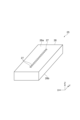
- FIG. 3 is a perspective view showing a glass substrate provided in the optical connecting part of FIG.
- FIG. 4 is an enlarged perspective view of a portion of the glass substrate shown in FIG.
- FIG. 5 is a graph for explaining a method of calculating the surface roughness Rz.
- FIG. 6A is a perspective view showing a state in which glass fibers are inserted into the through-holes of the glass substrate of FIG.
- FIG. 6A is a perspective view showing a state in which glass fibers are inserted into the through-holes of the glass substrate of FIG.
- FIG. 6B is a cross-sectional view of the glass substrate taken along line A1-A1 in FIG. 6A.
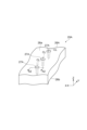
- FIG. 7A is an enlarged perspective view showing another example of a glass substrate.
- FIG. 7B is a cross-sectional view of the glass substrate taken along line A2-A2 in FIG. 7A.
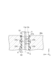
- FIG. 8 is a plan view showing another example of the shape of the through hole in the glass substrate.
- the manufacturing method tends to cause surface roughness on the inner surface of the through hole.
- the unevenness causes stress concentration on the glass fiber, which may cause damage such as breakage of the glass fiber.
- the inner diameter of the through hole is increased in this way, the positional accuracy of the glass fiber inserted into the through hole may be reduced.
- the present disclosure provides a glass substrate and optical connection components that can increase the positional accuracy of the glass fiber while reducing damage to the glass fiber.
- a glass substrate includes a first surface and a second surface opposite to the first surface, and includes a substrate body formed of a glass material.
- the substrate body is formed with at least one through hole penetrating from the first surface to the second surface and into which at least one glass fiber can be inserted.
- the outer diameter of the glass fiber is 125 ⁇ m or less.
- the inner diameter of the through hole is larger than the outer diameter of the glass fiber.
- the surface roughness Rz of the inner surface of the through hole is 1 ⁇ m or less.
- the ratio of the inner diameter of the through hole to the surface roughness Rz is 127 or less.
- the above glass substrate holds the glass fiber so that the glass fiber is maintained at a predetermined connection position relative to the electronic component to which it is connected.
- the optical coupling efficiency of the glass fiber to such an electronic substrate depends greatly on the positional accuracy of the glass fiber. For example, a positional deviation of the glass fiber on the order of ⁇ m can cause a large optical connection loss of the glass fiber. From the viewpoint of reducing such optical connection loss, it is desirable that the position of the glass fiber is precisely maintained on the order of ⁇ m.
- the surface roughness Rz of the inner surface of the through hole into which the glass fiber is inserted is set to 1 ⁇ or less, and further, assuming that a glass fiber having a standard outer diameter of 125 ⁇ m or less is inserted into the through hole, the ratio of the inner diameter of the through hole to the surface roughness Rz is set to 127 or less.
- the inner diameter of the through hole can be made as small as possible to a degree that does not cause damage to the glass fiber due to stress concentration on the glass fiber due to unevenness that may be formed on the inner surface of the through hole, and to a degree that allows adhesive between the inner surface of the through hole and the glass fiber.
- the maximum height of the convex portion that can be formed on the inner surface and the minimum space that can accommodate the adhesive injected into the through hole can be maintained between the inner surface of the through hole and the glass fiber, while minimizing the positional deviation of the glass fiber inserted into the through hole on the order of ⁇ m.
- the substrate body may be formed with a plurality of through holes into which a plurality of glass fibers can be inserted, respectively.
- the substrate body may be formed with a plurality of through holes into which a plurality of glass fibers can be inserted, respectively.
- a plurality of convex portions may be formed on the inner surface of the through hole along the extending direction of the through hole and the circumferential direction of the through hole.
- the arrangement pitch of two adjacent convex portions in the extending direction may be larger than the arrangement pitch of two adjacent convex portions in the circumferential direction.
- the number of convex portions formed along the extending direction can be reduced compared to the case where the arrangement pitch of each convex portion in the extending direction is equal to the arrangement pitch of each convex portion in the circumferential direction.
- the through hole may include an expanded portion connected to the first surface and expanding in diameter as it approaches the first surface.
- the inner surface of the expanded portion may be curved so as to move away from the central axis as it approaches the first surface.
- the through hole includes an expanded portion that expands in diameter as it approaches the first surface, and the inner surface of the expanded portion is curved so as to move away from the central axis as it approaches the first surface.
- the through hole includes an expanded portion that expands in diameter as it approaches the first surface, and the inner surface of the expanded portion is curved so as to move away from the central axis as it approaches the first surface.
- the inner surface of the enlarged diameter portion may be bent at the cut surface so that the curvature of the inner surface increases as it approaches the first surface. In this case, it is possible to more reliably reduce the occurrence of stress concentration on the glass fiber due to unevenness that may be formed on the inner surface of the enlarged diameter portion, and therefore it is possible to more reliably reduce damage to the glass fiber due to stress concentration.
- a groove extending from the first surface to the second surface may be formed.
- the groove formed on the inner surface of the through hole can be used as an escape groove to allow excess adhesive injected into the through hole to escape in order to fix the glass fiber to the substrate body.
- this escape groove it is not necessary to make adjustments such as designing the through hole to be large in advance in consideration of the amount of adhesive injected into the through hole, and it is possible to make the inner diameter of the through hole as small as possible while maintaining the shape of the inner surface of the through hole in a shape corresponding to the shape of the glass fiber. This makes it possible to more reliably obtain the above-mentioned effect of increasing the positional accuracy of the glass fiber inserted into the through hole.
- An optical connection part may include a glass substrate as described in any one of (1) to (6) above, and a glass fiber inserted into the through hole and fixed to the substrate body with an adhesive. Since this optical connection part includes any one of the glass substrates described above, as described above, it is possible to increase the positional accuracy of the glass fiber while reducing the occurrence of damage to the glass fiber.
- the glass fiber may include a first straight portion that extends along the extension direction of the through hole and is inserted into the through hole, a second straight portion that extends along a cross direction that crosses the extension direction, and a curved portion that extends between the first straight portion and the second straight portion while curving to connect the first straight portion and the second straight portion.
- FIG. 1 is a perspective view showing an optical connection part 1 according to this embodiment connected to an electronic board 2.
- FIG. 2A is a perspective view showing the optical connection part 1 of FIG. 1.
- FIG. 2B is a plan view of the optical connection part 1 of FIG. 2A as seen from the electronic board 2 side.
- the optical connection part 1 includes, for example, a fiber ribbon 10 and a fiber fixing part 20.
- the fiber ribbon 10 has a curved portion in the middle, and a first end of the fiber ribbon 10 is connected to the electronic board 2 via the fiber fixing part 20.
- a second end of the fiber ribbon 10 is connected to on-site wiring, for example, via a connector.
- the electronic board 2 may be, for example, a chip board such as a silicon photonics chip (SPC) that inputs and outputs light.
- SPC silicon photonics chip
- the fiber ribbon 10 includes, for example, a plurality of optical fibers 13 arranged in a row along the Y-axis direction, and a coating resin layer 15 that collectively coats the plurality of optical fibers 13 with a ribbon resin.
- Each of the plurality of optical fibers 13 may be, for example, a single-core optical fiber having a single core, or a multi-core optical fiber having multiple cores.
- Each optical fiber 13 includes at least a glass fiber 11.
- the glass fiber 11 includes, for example, a straight portion P1 (an example of a "second straight portion” in the present disclosure), a curved portion P2, and a straight portion P3 (an example of a "first straight portion” in the present disclosure).
- the straight portion P1 extends from the coating resin layer 15 in the X-axis direction (an example of a "crossing direction” in the present disclosure).
- the curved portion P2 is bent from the straight portion P1 in the Z-axis direction (an example of an "extending direction” in the present disclosure).
- the straight portion P3 extends from the curved portion P2 in the Z-axis direction and is connected to the fiber fixing component 20.
- the curved portion P2 extends between the straight portion P1 and the straight portion P3 while curving to connect the straight portion P1 and the straight portion P3.
- the curved portion P2 is formed, for example, by heating the glass fiber 11.
- the fiber fixing part 20 includes at least a glass substrate 25.
- the glass substrate 25 is placed on the electronic substrate 2 and holds each glass fiber 11 connected to the electronic substrate 2.
- the fiber fixing part 20 may further include a ferrule that is placed on the glass substrate 25 and supports each glass fiber 11.
- the glass substrate 25 is fixed to the electronic substrate 2 by, for example, an ultraviolet-curing adhesive.
- the glass substrate 25 is formed of a glass material that is capable of transmitting ultraviolet light. Examples of materials for the glass substrate 25 include fused quartz glass and borosilicate glass. Being capable of transmitting ultraviolet light means, for example, that a transmittance of 10% or more is achieved when a material with a thickness of 1 mm is irradiated with ultraviolet light having a wavelength of 350 nm or more and 400 nm or less.
- the glass substrate 25 includes, for example, a rectangular plate-shaped substrate body 26.
- the substrate body 26 includes a rectangular front surface 26a (an example of the "first surface” of the present disclosure) and a rectangular back surface 26b (an example of the "second surface” of the present disclosure) disposed on the opposite side to the front surface 26a.
- the front surface 26a and the back surface 26b extend along the X-axis direction and the Y-axis direction, respectively, and are aligned along the Z-axis direction.
- the back surface 26b faces the electronic substrate 2 (see FIG. 1) in the Z-axis direction.
- the back surface 26b is fixed to the electronic substrate 2 with, for example, the above-mentioned ultraviolet-curing adhesive.
- the thickness of the substrate body 26 between the front surface 26a and the back surface 26b may be, for example, about 1 mm.
- the substrate body 26 has a plurality of through holes 27 formed therein, penetrating in the Z-axis direction from the rear surface 26b to the front surface 26a.
- the plurality of through holes 27 are arranged in a line along the Y-axis direction so as to correspond to the plurality of glass fibers 11 (see FIG. 1) arranged along the Y-axis direction.
- the shape of each through hole 27 as viewed along the Z-axis direction is, for example, circular.
- the inner diameter D27 (see FIG. 4) of each through hole 27 may be constant at each position along the Z-axis direction. That is, each through hole 27 may have a constant inner diameter D27 from the front surface 26a to the rear surface 26b.
- Each through hole 27 can be made, for example, by using a laser-based hole-making technique.
- a process that combines photolithography and dry etching such as reactive ion etching (RIE) may be used.
- RIE reactive ion etching
- each through hole 27 is formed by laser irradiation and etching.
- a part of the substrate body 26 is modified by laser irradiation, and the modified part is removed by etching.
- each through hole 27 is formed in the substrate body 26.
- the inner surface 27a has surface roughness due to the formation method, such as laser irradiation and etching. As a result, fine irregularities are formed on the inner surface 27a.
- FIG. 4 shows multiple protrusions 27b formed on the inner surface 27a, but in reality, multiple recesses are also formed on the inner surface 27a.
- the multiple protrusions 27b are arranged side by side on the inner surface 27a, for example, along the Z-axis direction in which the central axis CL of the through hole 27 extends, and along the circumferential direction D centered on the central axis CL.
- Each protrusion 27b has a shape that extends in the Z-axis direction, for example.
- the arrangement pitch W1 of two adjacent convex portions 27b in the Z-axis direction is larger than the arrangement pitch W2 of two adjacent convex portions 27b in the circumferential direction D.
- the arrangement pitches W1, W2 of two adjacent convex portions 27b may be, for example, the distance between the centers of the two convex portions 27b when viewed along the normal direction of the inner surface 27a.
- the degree of unevenness of the inner surface 27a can be evaluated, for example, by the surface roughness Rz.
- the surface roughness Rz is calculated as the sum of the maximum peak height and the maximum valley depth of the profile curve over the reference length.
- Surface roughness Rz refers to the maximum height roughness defined in JIS B 0601:2013 "Geometric characteristics of products (GPS) - Surface quality: Profile curve method - Terms, definitions and surface quality parameters".
- Surface roughness Rz is a value measured in accordance with the description in JIS B 0601:2013.
- FIG. 5 is a graph for explaining a method for calculating surface roughness Rz.
- the horizontal axis of FIG. 5 indicates the position of the inner surface 27a along the circumferential direction D of the through hole 27.
- the vertical axis of FIG. 5 indicates the height of the unevenness of the inner surface 27a.
- the height of the highest convex portion 27b (maximum peak height) is represented as Zp
- the depth of the lowest concave portion maximum valley depth
- the surface roughness Rz is defined as the difference between the maximum peak height Zp and the maximum valley depth Zv (Zp-Zv).
- the glass fiber 11 inserted into the through hole 27 may come into contact with the convex portions 27b of the inner surface 27a, causing stress concentration at the contact points between the glass fiber 11 and the convex portions 27b.
- stress concentration may cause damage to the glass fiber 11, such as breakage. Therefore, from the perspective of reducing damage to the glass fiber 11, it is desirable for the surface roughness Rz of the inner surface 27a to be small.
- the surface roughness Rz of the inner surface 27a is set to 0 ⁇ m or more and 1 ⁇ m or less.
- the upper limit of the surface roughness Rz is not limited to 1 ⁇ m or less, and may be a value of 0.8 ⁇ m or less, 0.6 ⁇ m or less, or 0.4 ⁇ m or less.
- the inner diameter D27 of the through hole 27 is set to be smaller according to the surface roughness Rz.
- the inner diameter D27 is set so that the ratio of the inner diameter D27 to the surface roughness Rz is 127 or less. For example, when the surface roughness Rz is 1 ⁇ m, the inner diameter D27 of the through hole 27 may be 127 ⁇ m.
- the surface roughness Rz of the inner surface 27a can be adjusted by changing the laser irradiation conditions and etching conditions when forming the through-holes 27 in the substrate body 26. For example, by changing the irradiation pitch when irradiating the substrate body 26 with a laser and changing the etching process time, it is possible to obtain an inner surface 27a with a surface roughness Rz of 1 ⁇ m or less.
- FIG. 6A is a perspective view showing a state in which glass fibers 11 are inserted into each through hole 27 of the glass substrate 25 of FIG. 4.
- FIG. 6B is a cross-sectional view of the glass substrate 25 taken along line A1-A1 of FIG. 6A.
- each glass fiber 11 includes a core 11a and a cladding 11b surrounding the core 11a.
- the core 11a and the cladding 11b include, for example, silica-based glass.
- the outer diameter D11 of each glass fiber 11 may be, for example, 125 ⁇ m.
- the outer diameter D11 of each glass fiber 11 may be, for example, 80 ⁇ m or more and 125 ⁇ m or less.
- each glass fiber 11 is inserted into each through-hole 27 from the surface 26a of the substrate body 26, and an ultraviolet-curing adhesive A is injected into each through-hole 27.
- an ultraviolet-curing adhesive A is injected into each through-hole 27.
- each glass fiber 11 is fixed to the substrate body 26.
- the core 11a of each glass fiber 11 fixed to the substrate body 26 is optically connected to each input/output unit of the electronic board 2 (see FIG. 1) on which the substrate body 26 is mounted.
- the outer diameter D11 of the glass fiber 11 is 125 ⁇ m
- the inner diameter D27 of the through hole 27 is 127 ⁇ m
- the surface roughness Rz is 1 ⁇ m or less.
- the gap G1 between the glass fiber 11 and the inner surface 27a is 2 ⁇ m.
- the maximum height H of the convex portion 27b from the inner surface 27a is 1 ⁇ m, so that a gap G2 of at least 1 ⁇ m is maintained between the convex portion 27b and the glass fiber 11. In this case, it is possible to insert the glass fiber 11 into the through hole 27 while reducing the occurrence of damage to the glass fiber 11 caused by the stress concentration on the glass fiber 11 by the convex portion 27b.
- the glass fiber 11 is fixed to the substrate body 26 by adhesive A, so a space capable of injecting adhesive A is required between the glass fiber 11 and the inner surface 27a.
- a gap G2 of at least 1 ⁇ m is maintained between the glass fiber 11 and the convex portion 27b, so a space capable of injecting adhesive A is maintained between the glass fiber 11 and the inner surface 27a. Therefore, in this embodiment, it is possible to insert the glass fiber 11 into the through hole 27 without damaging the glass fiber 11, while maintaining a space capable of accepting adhesive A between the glass fiber 11 and the inner surface 27a.
- the glass substrate 25 holds the glass fiber 11 so that the glass fiber 11 is maintained at a predetermined connection position relative to the electronic substrate 2.
- the optical coupling efficiency of the glass fiber 11 relative to the electronic substrate 2 depends heavily on the positional accuracy of the glass fiber 11.
- a positional deviation of the glass fiber 11 on the order of ⁇ m can cause a large optical connection loss of the glass fiber 11. From the viewpoint of reducing such optical connection loss, it is desirable that the position of the glass fiber 11 is precisely maintained on the order of ⁇ m.
- the surface roughness Rz of the inner surface 27a into which the glass fiber 11 is inserted is set to 1 ⁇ or less, and furthermore, assuming that a glass fiber 11 having a standard outer diameter D11 of 125 ⁇ m or less is inserted into the through hole 27, the ratio of the inner diameter D27 of the through hole 27 to the surface roughness Rz is set to 127 or less.
- the inner diameter D27 of the through hole 27 can be made as small as possible to prevent damage to the glass fiber 11 due to stress concentration on the glass fiber 11 by the convex portion 27b of the inner surface 27a, and to a degree that allows adhesive A to be applied between the inner surface 27a and the glass fiber 11.
- the substrate body 26 is formed with a plurality of through holes 27 into which the plurality of glass fibers 11 can be inserted.
- the substrate body 26 is formed with a plurality of through holes 27 into which the plurality of glass fibers 11 can be inserted.
- the arrangement pitch W1 of two adjacent convex portions 27b in the Z-axis direction is larger than the arrangement pitch W2 of two adjacent convex portions 27b in the circumferential direction D.
- the number of convex portions 27b formed along the Z-axis direction can be reduced compared to the case where the arrangement pitch W1 of each convex portion 27b in the Z-axis direction is equal to the arrangement pitch W2 of each convex portion 27b in the circumferential direction D.
- the number of convex portions 27b that the glass fiber 11 comes into contact with while inserting the glass fiber 11 into the through hole 27 along the Z-axis direction from the front surface 26a to the back surface 26b can be reduced.
- the opportunity for stress concentration to occur in the glass fiber 11 due to contact of the glass fiber 11 with the convex portions 27b can be reduced, and damage to the glass fiber 11 caused by stress concentration can be more reliably reduced.
- the optical connection part 1 includes a glass substrate 25 and a glass fiber 11 that is inserted into the through hole 27 and fixed to the substrate body 26 with adhesive A. Because the optical connection part 1 includes the above-mentioned glass substrate 25, as described above, it is possible to increase the positional accuracy of the glass fiber 11 while reducing the occurrence of damage to the glass fiber 11.
- the glass fiber 11 includes a straight portion P1 that extends along the Z-axis direction and is inserted into the through hole 27, a straight portion P3 that extends along the X-axis direction, and a curved portion P2 that extends between the straight portion P1 and the straight portion P3 while curving to connect the straight portion P1 and the straight portion P3.
- a straight portion P1 that extends along the Z-axis direction and is inserted into the through hole 27, a straight portion P3 that extends along the X-axis direction, and a curved portion P2 that extends between the straight portion P1 and the straight portion P3 while curving to connect the straight portion P1 and the straight portion P3.
- FIG. 7A is an enlarged perspective view of glass substrate 25A, which is another example of glass substrate 25.
- FIG. 7B is a cross-sectional view of glass substrate 25A taken along line A2-A2 in FIG. 7A.
- the difference between glass substrate 25A in FIG. 7A and glass substrate 25 in the embodiment described above is the shape of each of the through holes formed in the substrate body.
- each through hole 27A of the substrate body 26A includes a constant diameter portion P21 and an expanding diameter portion P22.
- the constant diameter portion P21 extends in the Z-axis direction from the back surface 26b to the front surface 26a and has a constant inner diameter.
- the expanding diameter portion P22 extends in the Z-axis direction from the constant diameter portion P21 to the front surface 26a and expands in diameter as it approaches the front surface 26a.
- the inner diameter D21 of the constant diameter portion P21 is set to be, for example, larger than the outer diameter D11 of the glass fiber 11 (see FIG. 6A) and the inner diameter D21 relative to the surface roughness Rz is 127 ⁇ m or less. For example, if the outer diameter D11 of the glass fiber 11 is 125 ⁇ m and the surface roughness Rz is 1 ⁇ m or less, the inner diameter D21 of the constant diameter portion P21 may be 127 ⁇ m.
- the inner diameter D22 of the expanded diameter portion P22 gradually increases as it approaches the surface 26a from the constant diameter portion P21.
- the inner surface 27a of the expanded diameter portion P22 is curved so as to move away from the central axis CL of the through hole 27A as it approaches the surface 26a.
- the closer the inner surface 27a of the expanded diameter portion P22 is to the surface 26a the larger the distance d22 in the X-axis direction between the inner surface 27a and the central axis CL of the through hole 27A becomes.
- the cross section of FIG. 7B is a cut surface of the substrate body 26 cut along the central axis CL of the through hole 27A, i.e., a cut surface of the substrate body 26 taken on a plane passing through the central axis CL of the through hole 27A.
- the inner surface 27a of the expanded diameter portion P22 is bent so that the curvature of the inner surface 27a increases as it approaches the surface 26a.
- the curvature of the inner surface 27a is minimum at the connection portion P23 between the expanded diameter portion P22 and the constant diameter portion P21, and is maximum at the surface 26a.
- the inner diameter D22 of the expanded diameter portion P22 at the surface 26a is larger than the inner diameter D21 of the constant diameter portion P21.
- the inner diameter D22 of the expanded diameter portion P22 at the surface 26a may be 250 ⁇ m or less.
- the unevenness that may be formed on the inner surface 27a is omitted, but in reality, unevenness may be formed on the inner surface 27a as in the above-mentioned embodiment.
- through hole 27A includes expanding portion P22 whose diameter expands as it approaches surface 26a, and inner surface 27a of expanding portion P22 is curved so as to bend away from central axis CL as it approaches surface 26a.
- expanding portion P22 whose diameter expands as it approaches surface 26a
- inner surface 27a of expanding portion P22 is curved so as to bend away from central axis CL as it approaches surface 26a.
- inner surface 27a of enlarged portion P22 is bent so that the curvature of inner surface 27a increases as it approaches surface 26a. In this case, it is possible to more reliably reduce the occurrence of stress concentration on glass fiber 11 due to unevenness on inner surface 27a of enlarged portion P22, and therefore more reliably reduce damage to glass fiber 11 caused by stress concentration.
- FIG. 8 are plan views showing other examples of the shape of the through hole 27.
- the outer shape of the glass fiber 11 is also shown by a two-dot chain line.
- the shape of the through hole 27 seen along the Z-axis direction may be rectangular like the through hole 27B in (a) of FIG. 8, elliptical like the through hole 27C in (b) of FIG. 8, triangular like the through hole 27D in (c) of FIG. 8, or rhombus like the through hole 27E in (d) of FIG. 8.
- the shape of the through hole 27 seen along the Z-axis direction may be another polygon.
- two grooves 28a, 28b may be formed in a circular through-hole 27F.
- the two grooves 28a, 28b may extend along the Z-axis direction from the front surface 26a to the back surface 26b.
- Each groove 28a, 28b may be formed, for example, at a pair of positions in the through-hole 27F that face each other across the central axis CL.
- the shape of each groove 28a, 28b when viewed along the Z-axis direction may be, for example, rectangular.
- These grooves 28a, 28b can be used as escape grooves to allow excess adhesive A for fixing the glass fiber 11 to escape.
- escape grooves it is not necessary to make adjustments such as designing the through hole 27F to be large in advance in consideration of the amount of adhesive A injected into the through hole 27F, so the inner diameter of the through hole 27F can be made as small as possible while maintaining the shape of the through hole 27F to match the shape of the glass fiber 11. This makes it possible to more reliably obtain the above-mentioned effect of increasing the positional accuracy of the glass fiber 11 inserted into the through hole 27F.
- three grooves 29a, 29b, 29c may be formed in the through hole 27G. The number of grooves formed in the through hole in this way can be changed as appropriate.
- the glass substrate 25 holds one fiber ribbon 10.
- the glass substrate of the present disclosure may hold multiple fiber ribbons.
- the number of through holes formed in the glass substrate of the present disclosure can be changed as appropriate depending on the number of glass fibers to be inserted into the through holes.
- the glass substrate may be formed with one through hole for holding one glass fiber.
Landscapes
- Physics & Mathematics (AREA)
- General Physics & Mathematics (AREA)
- Optics & Photonics (AREA)
- Mechanical Coupling Of Light Guides (AREA)
- Optical Couplings Of Light Guides (AREA)
Abstract
本開示のガラス基板(25)は、第一面(26a)、および第一面(26a)とは反対側に位置する第二面(26b)を含み、ガラス材料によって形成された基板本体を備える。基板本体には、第一面(26a)から第二面(26b)まで貫通し、少なくとも一本のガラスファイバ(11)を挿入可能な少なくとも一本の貫通孔(27)が形成されている。ガラスファイバ(11)の外径は、125μm以下である。貫通孔(27)の内径は、ガラスファイバ(11)の外径よりも大きい。貫通孔(27)の内面の表面粗さRzは、1μm以下である。表面粗さRzに対する貫通孔(27)の内径の比率は、127以下である。
Description
本開示は、ガラス基板および光接続部品に関する。
本出願は、2023年6月9日出願の日本出願第2023-095677号に基づく優先権を主張し、前記日本出願に記載された全ての記載内容を援用する。
本出願は、2023年6月9日出願の日本出願第2023-095677号に基づく優先権を主張し、前記日本出願に記載された全ての記載内容を援用する。
特許文献1は、複数のガラスファイバを保持する多孔ガラス板を開示する。この多孔ガラス板は、複数のガラスファイバがそれぞれ挿入される複数の貫通孔が形成されたガラス板本体を有する。ガラス板本体は、例えば、レーザー改質とエッチングとを組み合わせたプロセス、或いはレーザーを用いた孔空け技術を用いて形成される。
本開示の一実施形態に係るガラス基板は、第一面、および第一面とは反対側に位置する第二面を含み、ガラス材料によって形成された基板本体を備える。基板本体には、第一面から第二面まで貫通し、少なくとも一本のガラスファイバを挿入可能な少なくとも一本の貫通孔が形成されている。ガラスファイバの外径は、125μm以下である。貫通孔の内径は、ガラスファイバの外径よりも大きく、貫通孔の内面の表面粗さRzは、1μm以下である。表面粗さRzに対する貫通孔の内径の比率は、127以下である。
[本開示が解決しようとする課題]
上述したような製造方法を用いてガラス板本体に貫通孔を形成した場合、その製造方法に起因して貫通孔の内面に表面荒れが発生する傾向がある。表面荒れによって貫通孔の内面に凹凸が形成されると、凹凸によるガラスファイバへの応力集中の発生に起因して、ガラスファイバに断線などの損傷が生じ得る。このようなガラスファイバの損傷の発生を低減するために、例えば、貫通孔の内面に生じ得る凹凸の高さを加味して貫通孔の内径を予め大きくすることが考えられる。しかしながら、このように貫通孔の内径を大きくすると、貫通孔に挿入されるガラスファイバの位置精度が低下するおそれがある。
上述したような製造方法を用いてガラス板本体に貫通孔を形成した場合、その製造方法に起因して貫通孔の内面に表面荒れが発生する傾向がある。表面荒れによって貫通孔の内面に凹凸が形成されると、凹凸によるガラスファイバへの応力集中の発生に起因して、ガラスファイバに断線などの損傷が生じ得る。このようなガラスファイバの損傷の発生を低減するために、例えば、貫通孔の内面に生じ得る凹凸の高さを加味して貫通孔の内径を予め大きくすることが考えられる。しかしながら、このように貫通孔の内径を大きくすると、貫通孔に挿入されるガラスファイバの位置精度が低下するおそれがある。
本開示は、ガラスファイバの損傷を低減しつつ、ガラスファイバの位置精度を高めることができるガラス基板および光接続部品を提供する。
[本開示の効果]
本開示によるガラス基板および光接続部品によれば、ガラスファイバの損傷を低減しつつ、ガラスファイバの位置精度を高めることができる。
本開示によるガラス基板および光接続部品によれば、ガラスファイバの損傷を低減しつつ、ガラスファイバの位置精度を高めることができる。
[本開示の実施形態の説明]
最初に、本開示の実施形態の内容を列記して説明する。
最初に、本開示の実施形態の内容を列記して説明する。
(1)本開示の一実施形態に係るガラス基板は、第一面、および第一面とは反対側に位置する第二面を含み、ガラス材料によって形成された基板本体を備える。基板本体には、第一面から第二面まで貫通し、少なくとも一本のガラスファイバを挿入可能な少なくとも一本の貫通孔が形成されている。ガラスファイバの外径は、125μm以下である。貫通孔の内径は、ガラスファイバの外径よりも大きい。貫通孔の内面の表面粗さRzは、1μm以下である。表面粗さRzに対する貫通孔の内径の比率は、127以下である。
上記のガラス基板は、例えば、接続相手の電子部品に対してガラスファイバが所定の接続位置に維持されるように、ガラスファイバを保持する。このような電子基板に対するガラスファイバの光結合効率は、ガラスファイバの位置精度に大きく依存する。例えば、ガラスファイバのμmオーダーの位置ずれが、ガラスファイバの大きな光接続損失を生じさせ得る。このような光接続損失を低減する観点からは、ガラスファイバの位置がμmオーダーで精密に維持されていることが望ましい。上記のガラス基板では、ガラスファイバが挿入される貫通孔の内面の表面粗さRzが1μ以下に設定され、更に、標準的な125μm以下の外径を有するガラスファイバが貫通孔に挿入されることを想定して、表面粗さRzに対する貫通孔の内径の比率が127以下に設定されている。この場合、貫通孔の内面に形成され得る凹凸によるガラスファイバへの応力集中に起因するガラスファイバの損傷が生じない程度に、且つ貫通孔の内面とガラスファイバとの間に接着剤を許容可能な程度に、貫通孔の内径を極力小さくできる。つまり、内面に形成され得る最大高さの凸部、および貫通孔に注入される接着剤を許容可能な最小限のスペースを、貫通孔の内面とガラスファイバとの間に維持しながら、貫通孔に挿入されるガラスファイバの位置ずれをμmオーダーで極力小さくできる。その結果、貫通孔の凹凸によるガラスファイバへの応力集中に起因するガラスファイバの損傷の発生を低減しつつ、ガラス基板に保持されるガラスファイバの位置精度を高めることが可能となる。
(2)上記(1)に記載のガラス基板において、基板本体には、複数のガラスファイバをそれぞれ挿入可能な複数の貫通孔が形成されていてもよい。この場合、複数のガラスファイバのそれぞれの損傷の発生を低減しつつ、ガラス基板に保持される各ガラスファイバの位置精度を高めることが可能となるので、上述した効果を効果的に得ることができる。
(3)上記(1)又は(2)に記載のガラス基板において、貫通孔の内面には、貫通孔が延びる延在方向及び貫通孔の周方向に沿って並ぶ複数の凸部が形成されていてもよい。延在方向において互いに隣り合う二つの凸部の配列ピッチは、周方向において互いに隣り合う二つの凸部の配列ピッチよりも大きくてもよい。この場合、延在方向の各凸部の配列ピッチと周方向の各凸部の配列ピッチとが等しい場合に比べて、延在方向に沿って形成される凸部の数を減らすことができる。つまり、第一面から第二面までガラスファイバを貫通孔へ延在方向に沿って挿入させる間にガラスファイバが接触する凸部の数を減らすことができる。その結果、凸部によってガラスファイバに応力集中が発生する機会を低減でき、応力集中に起因するガラスファイバの損傷をより確実に低減できる。
(4)上記(1)から(3)のいずれかに記載のガラス基板において、貫通孔は、第一面に接続され、第一面に近づくにつれて拡径する拡径部を含んでもよい。貫通孔の中心軸を通る平面での基板本体の切断面において、拡径部の内面は、第一面に近づくにつれて中心軸から遠ざかるように曲げられた曲線状であってもよい。例えば、ガラスファイバを第一面から貫通孔に挿入する場合に、第一面付近の貫通孔の内面に形成され得る凹凸によってガラスファイバに応力集中が生じやすい。これに対し、上記の構成では、貫通孔が、第一面に近づくにつれて拡径する拡径部を含んでおり、拡径部の内面は、第一面に近づくにつれて中心軸から遠ざかるように曲げられた曲線状である。この場合、拡径部の内面に形成され得る凹凸によるガラスファイバへの応力集中の発生を低減できるので、応力集中に起因するガラスファイバの損傷をより確実に低減することが可能となる。
(5)上記(4)に記載のガラス基板において、切断面において、拡径部の内面は、第一面に近づくにつれて内面の曲率が大きくなるように曲げられていてもよい。この場合、拡径部の内面に形成され得る凹凸によるガラスファイバへの応力集中の発生をより確実に低減できるので、応力集中に起因するガラスファイバの損傷をより一層確実に低減することが可能となる。
(6)上記(1)から(5)のいずれかに記載のガラス基板において、第一面から第二面にわたって延びる溝が形成されていてもよい。この場合、貫通孔の内面に形成される溝は、ガラスファイバを基板本体に固定するために貫通孔に注入される接着剤の余剰分を逃がす逃げ溝として利用できる。この逃げ溝を利用すれば、貫通孔への接着剤の注入量を考慮して貫通孔を予め大きく設計するなどの調整をしなくて済むため、貫通孔の内面の形状をガラスファイバの形状に対応した形状に維持しつつ、貫通孔の内径を極力小さくすることができる。これにより、貫通孔に挿入されるガラスファイバの位置精度を高めるとの上述した効果をより確実に得ることができる。
(7)本開示の一実施形態に係る光接続部品は、上記(1)から(6)のいずれかに記載のガラス基板と、貫通孔に挿入され、接着剤で基板本体に固定されているガラスファイバと、を備えてもよい。この光接続部品は、上述したいずれかのガラス基板を備えるので、上述したように、ガラスファイバの損傷の発生を低減しつつ、ガラスファイバの位置精度を高めることが可能となる。
(8)上記(7)に記載の光接続部品において、ガラスファイバは、貫通孔が延びる延在方向に沿って延び、貫通孔に挿入された第一直線部分と、延在方向に交差する交差方向に沿って延びる第二直線部分と、第一直線部分と第二直線部分との間において、湾曲しながら第一直線部分と第二直線部分とを結ぶように延びる湾曲部分と、を含んでもよい。この場合、ガラスファイバの低背化を図りつつ、ガラスファイバの損傷の低減およびガラスファイバの位置精度向上という上述した効果を得ることができる。
[本開示の実施形態の詳細]
本開示に係るガラス基板および光接続部品の具体例を、以下で図面を参照しながら説明する。本開示は、以下の例示に限定されるものではなく、請求の範囲に示され、請求の範囲と均等の範囲における全ての変更が含まれることが意図される。図面の説明において同一または相当する要素には同一の符号を付し、重複する説明を適宜省略する。図面について、理解の容易化のため、一部が簡略化または誇張して描いている場合があり、寸法比率等は図面に記載のものに限定されない。図面には必要に応じてXYZ座標系が示される。X軸方向、Y軸方向およびZ軸方向は、互いに交差(例えば直交)する。
本開示に係るガラス基板および光接続部品の具体例を、以下で図面を参照しながら説明する。本開示は、以下の例示に限定されるものではなく、請求の範囲に示され、請求の範囲と均等の範囲における全ての変更が含まれることが意図される。図面の説明において同一または相当する要素には同一の符号を付し、重複する説明を適宜省略する。図面について、理解の容易化のため、一部が簡略化または誇張して描いている場合があり、寸法比率等は図面に記載のものに限定されない。図面には必要に応じてXYZ座標系が示される。X軸方向、Y軸方向およびZ軸方向は、互いに交差(例えば直交)する。
図1は、本実施形態に係る光接続部品1が電子基板2に接続された状態を示す斜視図である。図2Aは、図1の光接続部品1を示す斜視図である。図2Bは、図2Aの光接続部品1を電子基板2側から見た平面図である。
図1に示されるように、光接続部品1は、例えば、ファイバリボン10と、ファイバ固定部品20と、を備える。ファイバリボン10は、その途中に湾曲部分を有しており、ファイバリボン10の第1端は、ファイバ固定部品20を介して電子基板2に接続されている。ファイバリボン10の第2端は、例えばコネクタを介して構内配線に接続される。電子基板2は、例えば、光の入出力を行うシリコンフォトニクスチップ(SPC:Silicon Photonics Chip)などのチップ基板としてよい。
ファイバリボン10は、例えば、Y軸方向に沿って一列に並べられた複数の光ファイバ13と、複数の光ファイバ13をリボン用樹脂によってまとめて被覆する被覆樹脂層15と、を備える。複数の光ファイバ13のそれぞれは、例えば、単一コアを有するシングルコア光ファイバであってもよいし、複数のコアを有するマルチコア光ファイバであってもよい。各光ファイバ13は、ガラスファイバ11を少なくとも含む。
図2Aに示されるように、ガラスファイバ11は、例えば、直線部分P1(本開示の「第二直線部分」の一例)と、湾曲部分P2と、直線部分P3(本開示の「第一直線部分」の一例)と、を含む。直線部分P1は、被覆樹脂層15からX軸方向(本開示の「交差方向」の一例)に延びている。湾曲部分P2は、直線部分P1からZ軸方向(本開示の「延在方向」の一例)に曲げられている。直線部分P3は、湾曲部分P2からZ軸方向に延び、ファイバ固定部品20に連結されている。湾曲部分P2は、直線部分P1と直線部分P3との間において、湾曲しながら直線部分P1と直線部分P3とを結ぶように延びている。湾曲部分P2は、例えば、ガラスファイバ11の加熱により形成される。
ファイバ固定部品20は、少なくともガラス基板25を含む。ガラス基板25は、電子基板2上に載置され、電子基板2に接続される各ガラスファイバ11を保持する。ファイバ固定部品20は、ガラス基板25上に載置されて各ガラスファイバ11を支持するフェルールを更に含んでもよい。ガラス基板25は、例えば、紫外線硬化型の接着剤によって電子基板2に固定されている。ガラス基板25は、紫外線を透過可能なガラス材料によって形成されている。ガラス基板25の材料としては、例えば、溶融石英ガラスまたはホウケイ酸ガラスなどが挙げられる。紫外線を透過可能とは、例えば、厚さ1mmの材料に波長350nm以上かつ400nm以下の紫外線を照射したときの透過率が10%以上であることをいう。
図3は、ガラス基板25を示す斜視図である。図4は、図3のガラス基板25の一部を拡大して示す斜視図である。図3に示されるように、ガラス基板25は、例えば、矩形板状の基板本体26を含む。基板本体26は、矩形状の表面26a(本開示の「第一面」の一例)と、表面26aとは反対側に配置される矩形状の裏面26b(本開示の「第二面」の一例)と、を含む。表面26aおよび裏面26bのそれぞれは、X軸方向およびY軸方向に沿って延びており、Z軸方向に沿って互いに並んでいる。裏面26bは、電子基板2(図1参照)とZ軸方向に対面する。裏面26bは、例えば、上述した紫外線硬化型の接着剤で電子基板2に固定されている。表面26aと裏面26bとの間の基板本体26の厚さは、例えば1mm程度としてよい。
基板本体26には、裏面26bから表面26aまでZ軸方向に貫通する複数の貫通孔27が形成されている。複数の貫通孔27は、Y軸方向に沿って並ぶ複数のガラスファイバ11(図1参照)にそれぞれ対応するように、Y軸方向に沿って一列に並べられている。Z軸方向に沿って見た各貫通孔27の形状は、例えば円形状である。各貫通孔27の内径D27(図4参照)は、Z軸方向に沿った各位置において一定であってよい。すなわち、各貫通孔27は、表面26aから裏面26bまで一定の内径D27を有してよい。
各貫通孔27は、例えば、レーザーを用いた孔開け技術を用いて作成可能である。各貫通孔27を形成する際、フォトリソグラフィと、反応性イオンエッチング(Reactive Ion Etching:RIE)などのドライエッチングと、を組み合わせたプロセスを用いてもよい。本実施形態では、各貫通孔27は、レーザーの照射とエッチングとを用いて形成される。例えば、レーザーの照射によって基板本体26の一部が改質され、その改質された部分がエッチングによって除去される。その結果、基板本体26に各貫通孔27が形成される。
図4に示されるように、内面27aには、レーザー照射およびエッチングといった形成方法に起因する表面荒れが生じている。その結果、内面27aには、微細な凹凸が形成されている。図4には、説明の便宜上、内面27aに形成される複数の凸部27bが示されているが、実際には、内面27aには複数の凹部も形成されている。複数の凸部27bは、例えば、内面27aにおいて、貫通孔27の中心軸CLが延びるZ軸方向、および中心軸CLを中心とする周方向Dに沿って、互いに並んで配置されている。各凸部27bは、例えば、Z軸方向に延びる形状を有する。
図4に示される例では、Z軸方向において互いに隣り合う2つの凸部27bの配列ピッチW1は、周方向Dにおいて互いに隣り合う2つの凸部27bの配列ピッチW2よりも大きい。互いに隣り合う2つの凸部27bの配列ピッチW1,W2は、例えば、内面27aの法線方向に沿って見た場合における2つの凸部27bの中心間の距離としてよい。
内面27aの凹凸高さの程度は、例えば、表面粗さRzによって評価できる。表面粗さRzは、基準長さにおける輪郭曲線の山高さの最大値と谷深さの最大値との和によって算出される。表面粗さRzは、JIS B 0601:2013「製品の幾何特性使用(GPS)-表面性状:輪郭曲線方式-用語、定義及び表面性状パラメータ」で規定される最大高さ粗さを意味する。表面粗さRzは、JIS B 0601:2013の記載に準拠して測定される値である。
図5は、表面粗さRzの算出方法を説明するためのグラフである。図5の横軸は、貫通孔27の周方向Dに沿った内面27aの位置を示している。図5の縦軸は、内面27aの凹凸高さを示している。図5のグラフG10において、内面27aの周方向に沿った基準長さの中で、最も高い凸部27bの高さ(最大山高さ)がZpとして表され、最も低い凹部の深さ(最大谷深さ)がZvとして表されている。この場合、表面粗さRzは、最大山高さZpと最大谷深さZvとの差(Zp-Zv)によって定義される。
表面粗さRzの大きさ、すなわち内面27aの凸部27bの高さによっては、貫通孔27に挿入されるガラスファイバ11が内面27aの凸部27bに接触し、ガラスファイバ11と凸部27bとの接触部分において応力集中が生じるおそれがある。このような応力集中の発生は、ガラスファイバ11に断線などの損傷を生じさせ得る。従って、ガラスファイバ11の損傷を低減する観点から、内面27aの表面粗さRzは小さいことが望ましい。
本実施形態において、内面27aの表面粗さRzは、0μm以上1μm以下に設定されている。表面粗さRzの上限値は、1μm以下に限らず、0.8μm以下、0.6μm以下、または0.4μm以下などの値であってもよい。貫通孔27の内径D27は、表面粗さRzに応じて小さくなるように設定される。本実施形態では、表面粗さRzに対する内径D27の比率が127以下となるように、内径D27が設定されている。例えば、表面粗さRzが1μmである場合、貫通孔27の内径D27は、127μmであってよい。
内面27aの表面粗さRzは、基板本体26に貫通孔27を形成する際のレーザー照射条件およびエッチング条件の変更によって調整可能である。例えば、基板本体26に対してレーザーを照射する際の照射ピッチの変更、およびエッチング処理時間の変更を行うことにより、1μm以下の表面粗さRzを有する内面27aを得ることができる。
図6Aは、図4のガラス基板25の各貫通孔27にガラスファイバ11が挿入された状態を示す斜視図である。図6Bは、図6AのA1-A1線に沿ったガラス基板25の断面図である。図6Aに示されるように、各ガラスファイバ11は、コア11aと、コア11aを取り囲むクラッド11bと、含む。コア11aおよびクラッド11bは、例えば、石英系ガラスを含む。各ガラスファイバ11の外径D11は、例えば、125μmとしてよい。各ガラスファイバ11の外径D11は、例えば、80μm以上125μm以下であってよい。
図6Bに示されるように、各ガラスファイバ11は、基板本体26の表面26aから各貫通孔27に挿入され、紫外線硬化型の接着剤Aが各貫通孔27に注入される。この接着剤Aが硬化することによって、各ガラスファイバ11が基板本体26に固定される。基板本体26に固定された各ガラスファイバ11のコア11aは、基板本体26が搭載される電子基板2(図1参照)の各入出力部に光接続される。
図6Bにおいて、ガラスファイバ11の外径D11が125μmであり、貫通孔27の内径D27が127μmであり、表面粗さRzが1μm以下である場合を想定する。この場合、貫通孔27にガラスファイバ11が挿入された状態(厳密には、ガラスファイバ11の光軸が貫通孔27の中心軸CLに一致するように配置された状態)において、ガラスファイバ11と内面27aとの隙間G1は2μmとなる。表面粗さRzが1μm以下である場合、内面27aからの凸部27bの最大高さHは1μmであるため、その凸部27bとガラスファイバ11との間には、少なくとも1μmの隙間G2が維持される。この場合、凸部27bによるガラスファイバ11への応力集中に起因するガラスファイバ11の損傷の発生を低減しながら、ガラスファイバ11を貫通孔27に挿入することが可能となる。
ガラスファイバ11は、上述したように、接着剤Aによって基板本体26に固定されるので、ガラスファイバ11と内面27aとの間に、接着剤Aを注入可能なスペースを要する。本実施形態では、ガラスファイバ11と凸部27bとの間に少なくとも1μmの隙間G2が維持されているので、ガラスファイバ11と内面27aとの間に接着剤Aを注入可能なスペースが維持されている。従って、本実施形態では、ガラスファイバ11と内面27aとの間に接着剤Aを許容可能なスペースを維持しつつ、ガラスファイバ11に損傷が生じないようにガラスファイバ11を貫通孔27に挿入することが可能である。
以上に説明した、本実施形態に係るガラス基板25および光接続部品1によって得られる効果について説明する。
ガラス基板25は、電子基板2に対してガラスファイバ11が所定の接続位置に維持されるように、ガラスファイバ11を保持する。ここで、電子基板2に対するガラスファイバ11の光結合効率は、ガラスファイバ11の位置精度に大きく依存する。例えば、ガラスファイバ11のμmオーダーの位置ずれが、ガラスファイバ11の大きな光接続損失を生じさせ得る。このような光接続損失を低減する観点からは、ガラスファイバ11の位置がμmオーダーで精密に維持されていることが望ましい。
本実施形態では、ガラスファイバ11が挿入される内面27aの表面粗さRzが1μ以下に設定され、更に、標準的な125μm以下の外径D11を有するガラスファイバ11が貫通孔27に挿入されることを想定して、表面粗さRzに対する貫通孔27の内径D27の比率が127以下に設定されている。この場合、内面27aの凸部27bによるガラスファイバ11への応力集中に起因するガラスファイバ11の損傷が発生しない程度に、且つ内面27aとガラスファイバ11との間に接着剤Aを許容可能な程度に、貫通孔27の内径D27を極力小さくできる。
つまり、内面27aの凸部27b、および貫通孔27に注入される接着剤Aを許容可能な最小限のスペースを、内面27aとガラスファイバ11との間に維持しながら、貫通孔27に挿入されるガラスファイバ11の位置ずれをμmオーダーで極力小さくできる。その結果、凸部27bによるガラスファイバ11への応力集中に起因するガラスファイバ11の損傷の発生を低減しつつ、ガラス基板25に保持されるガラスファイバ11の位置精度を高めることが可能となる。
本実施形態において、基板本体26には、複数のガラスファイバ11をそれぞれ挿入可能な複数の貫通孔27が形成されている。この場合、複数のガラスファイバ11のそれぞれの損傷の発生を低減しつつ、ガラス基板25に保持される各ガラスファイバ11の位置精度を高めることが可能となるので、上述した効果を効果的に得ることができる。
本実施形態において、Z軸方向において互いに隣り合う二つの凸部27bの配列ピッチW1は、周方向Dにおいて互いに隣り合う二つの凸部27bの配列ピッチW2よりも大きい。この場合、Z軸方向の各凸部27bの配列ピッチW1と周方向Dの各凸部27bの配列ピッチW2とが等しい場合に比べて、Z軸方向に沿って形成される凸部27bの数を減らすことができる。つまり、表面26aから裏面26bまでガラスファイバ11を貫通孔27へZ軸方向に沿って挿入させる間にガラスファイバ11が接触する凸部27bの数を減らすことができる。その結果、凸部27bへのガラスファイバ11の接触によってガラスファイバ11に応力集中が発生する機会を低減でき、応力集中に起因するガラスファイバ11の損傷をより確実に低減できる。
本実施形態において、光接続部品1は、ガラス基板25と、貫通孔27に挿入され、接着剤Aで基板本体26に固定されているガラスファイバ11と、を備えている。光接続部品1は、上述したガラス基板25を備えるので、上述したように、ガラスファイバ11の損傷の発生を低減しつつ、ガラスファイバ11の位置精度を高めることが可能となる。
本実施形態において、ガラスファイバ11は、Z軸向に沿って延び、貫通孔27に挿入された直線部分P1と、X軸方向に沿って延びる直線部分P3と、直線部分P1と直線部分P3との間において、湾曲しながら直線部分P1と直線部分P3とを結ぶように延びる湾曲部分P2と、を含んでいる。この場合、ガラスファイバ11の低背化を図りつつ、ガラスファイバ11の損傷の低減およびガラスファイバ11の位置精度の向上といった上述した効果を得ることができる。
本開示は、上述した実施形態に限られず、請求の範囲に記載された趣旨を逸脱しない範囲において適宜変更可能である。
図7Aは、ガラス基板25の別例であるガラス基板25Aを拡大して示す斜視図である。図7Bは、図7AのA2-A2線に沿ったガラス基板25Aの断面図である。図7Aのガラス基板25Aと、上述した実施形態のガラス基板25との相違点は、基板本体に形成される各貫通孔の形状である。
図7Bに示されるように、基板本体26Aの各貫通孔27Aは、定径部P21と、拡径部P22と、を含む。定径部P21は、裏面26bから表面26aに向かってZ軸方向に延び、一定の内径を有する。拡径部P22は、定径部P21から表面26aまでZ軸方向に延び、表面26aに近づくにつれて拡径する。定径部P21の内径D21は、例えば、ガラスファイバ11の外径D11(図6A参照)よりも大きく、且つ表面粗さRzに対する内径D21が127μm以下となるように設定される。例えば、ガラスファイバ11の外径D11が125μmであり、表面粗さRzが1μm以下である場合には、定径部P21の内径D21は、127μmとしてよい。
拡径部P22の内径D22は、定径部P21から表面26aに近づくにつれて徐々に大きくなるように変化している。図7Bの断面において、拡径部P22の内面27aは、表面26aに近づくにつれて貫通孔27Aの中心軸CLから遠ざかるように曲げられた曲線状である。その結果、図7Bの断面において、拡径部P22の内面27aが表面26aに近づくほど、内面27aと貫通孔27Aの中心軸CLとのX軸方向の距離d22が大きくなっている。図7Bの断面は、貫通孔27Aの中心軸CLに沿って切断された基板本体26の切断面、すなわち、貫通孔27Aの中心軸CLを通る平面での基板本体26の切断面である。
図7Bの断面において、拡径部P22の内面27aは、表面26aに近づくほど内面27aの曲率が大きくなるように曲げられている。その結果、拡径部P22と定径部P21との接続部分P23において内面27aの曲率は最小となり、表面26aにおいて内面27aの曲率は最大となる。表面26aにおける拡径部P22の内径D22は、定径部P21の内径D21よりも大きくなっている。例えば、定径部P21の内径D21が127μm以下である場合、表面26aにおける拡径部P22の内径D22は、250μm以下であってよい。図7Bの断面において、説明の便宜上、内面27aに形成され得る凹凸を省略して示しているが、実際には、上述した実施形態と同様、内面27aには凹凸が形成され得る。
このような形態であっても、上述した実施形態と同様の効果を得ることができる。更に、ガラス基板25Aでは、貫通孔27Aが、表面26aに近づくにつれて拡径する拡径部P22を含んでおり、拡径部P22の内面27aは、表面26aに近づくにつれて中心軸CLから遠ざかるように曲げられた曲線状である。この場合、拡径部P22の内面27aの凹凸によるガラスファイバ11への応力集中の発生を低減できるので、応力集中に起因するガラスファイバ11の損傷をより確実に低減することが可能となる。
ガラス基板25Aでは、拡径部P22の内面27aは、表面26aに近づくにつれて内面27aの曲率が大きくなるように曲げられている。この場合、拡径部P22の内面27aの凹凸によるガラスファイバ11への応力集中の発生をより確実に低減できるので、応力集中に起因するガラスファイバ11の損傷をより一層確実に低減することが可能となる。
図8の(a)から(f)は、貫通孔27の形状の別例を示す平面図である。図8の(a)から(f)には、ガラスファイバ11の外形が二点鎖線で併せて示されている。例えば、Z軸方向に沿って見た貫通孔27の形状は、図8の(a)の貫通孔27Bのように、矩形であってもよいし、図8の(b)の貫通孔27Cのように、楕円であってもよいし、図8の(c)の貫通孔27Dのように、三角であってもよいし、図8の(d)の貫通孔27Eのように、ひし形であってもよい。或いは、Z軸方向に沿って見た貫通孔27の形状は、他の多角形であってもよい。
図8の(e)に示されるように、円形の貫通孔27Fに二本の溝28a,28bが形成されていてもよい。二本の溝28a,28bは、表面26aから裏面26bにわたってZ軸方向に沿って延びていてもよい。各溝28a,28bは、例えば、貫通孔27Fのうち中心軸CLを挟んで互いに対面する一対の位置に形成されてよい。Z軸方向に沿って見た各溝28a,28bの形状は、例えば矩形であってよい。
これらの溝28a,28bは、ガラスファイバ11を固定するための接着剤Aの余剰分を逃がす逃げ溝として利用できる。この逃げ溝を利用すれば、貫通孔27Fへの接着剤Aの注入量を考慮して貫通孔27Fを予め大きく設計するなどの調整をしなくて済むため、貫通孔27Fの形状をガラスファイバ11の形状に沿った形状に維持しつつ、貫通孔27Fの内径を極力小さくすることができる。これにより、貫通孔27Fに挿入されるガラスファイバ11の位置精度を高めるとの上述した効果をより確実に得ることができる。図8の(f)に示されるように、三本の溝29a,29b,29cが貫通孔27Gに形成されてもよい。このように貫通孔に形成される溝の数は、適宜変更可能である。
上述した実施形態では、ガラス基板25が一つのファイバリボン10を保持する場合を説明した。しかし、本開示のガラス基板は、複数のファイバリボンを保持してもよい。本開示のガラス基板に形成される貫通孔の数は、貫通孔に挿入されるガラスファイバの数に応じて適宜変更可能である。例えば、ガラス基板には、一本のガラスファイバを保持するための一つの貫通孔が形成されてもよい。
1…光接続部品
2…電子基板
10…ファイバリボン
11…ガラスファイバ
11a…コア
11b…クラッド
13…光ファイバ
15…被覆樹脂層
20…ファイバ固定部品
27,27A,27B,27C,27D,27E,27F,27G…貫通孔
25,25A…ガラス基板
26a…表面(本開示の「第一面」の一例)
26b…裏面(本開示の「第二面」の一例)
27a…内面
27b…凸部
28a,28b,29a,29b,29c…溝
A…接着剤
CL…中心軸
D…周方向
D11…外径
D21,D22…内径
D27…内径
d22…距離
G1,G2…隙間
P1…直線部分(本開示の「第二直線部分」の一例)
P2…湾曲部分
P3…直線部分(本開示の「第一直線部分)の一例)
P21…定径部
P22…拡径部
P23…接続部分
W1,W2…配列ピッチ
2…電子基板
10…ファイバリボン
11…ガラスファイバ
11a…コア
11b…クラッド
13…光ファイバ
15…被覆樹脂層
20…ファイバ固定部品
27,27A,27B,27C,27D,27E,27F,27G…貫通孔
25,25A…ガラス基板
26a…表面(本開示の「第一面」の一例)
26b…裏面(本開示の「第二面」の一例)
27a…内面
27b…凸部
28a,28b,29a,29b,29c…溝
A…接着剤
CL…中心軸
D…周方向
D11…外径
D21,D22…内径
D27…内径
d22…距離
G1,G2…隙間
P1…直線部分(本開示の「第二直線部分」の一例)
P2…湾曲部分
P3…直線部分(本開示の「第一直線部分)の一例)
P21…定径部
P22…拡径部
P23…接続部分
W1,W2…配列ピッチ
Claims (8)
- 第一面、および前記第一面とは反対側に位置する第二面を含み、ガラス材料によって形成された基板本体を備え、
前記基板本体には、前記第一面から前記第二面まで貫通し、少なくとも一本のガラスファイバを挿入可能な少なくとも一本の貫通孔が形成されており、
前記ガラスファイバの外径は、125μm以下であり、
前記貫通孔の内径は、前記ガラスファイバの前記外径よりも大きく、
前記貫通孔の内面の表面粗さRzは、1μm以下であり、
前記表面粗さRzに対する前記貫通孔の前記内径の比率は、127以下である、
ガラス基板。 - 前記基板本体には、複数の前記ガラスファイバをそれぞれ挿入可能な複数の前記貫通孔が形成されている、
請求項1に記載のガラス基板。 - 前記貫通孔の前記内面には、前記貫通孔が延びる延在方向及び前記貫通孔の周方向に沿って並ぶ複数の凸部が形成されており、
前記延在方向において互いに隣り合う二つの前記凸部の配列ピッチは、前記周方向において互いに隣り合う二つの前記凸部の配列ピッチよりも大きい、
請求項1または請求項2に記載のガラス基板。 - 前記貫通孔は、前記第一面に接続され、前記第一面に近づくにつれて拡径する拡径部を含み、
前記貫通孔の中心軸を通る平面での前記基板本体の切断面において、前記拡径部の内面は、前記第一面に近づくにつれて前記中心軸から遠ざかるように曲げられた曲線状である、
請求項1から請求項3のいずれか一項に記載のガラス基板。 - 前記切断面において、前記拡径部の前記内面は、前記第一面に近づくにつれて前記内面の曲率が大きくなるように曲げられている、
請求項4に記載のガラス基板。 - 前記貫通孔の内面には、前記第一面から前記第二面にわたって延びる溝が形成されている、
請求項1から請求項5のいずれか一項に記載のガラス基板。 - 請求項1から請求項6のいずれか一項に記載の前記ガラス基板と、
前記貫通孔に挿入され、接着剤によって前記基板本体に固定されている前記ガラスファイバと、を備える、
光接続部品。 - 前記ガラスファイバは、
前記貫通孔が延びる延在方向に沿って延び、前記貫通孔に挿入された第一直線部分と、
前記延在方向に交差する交差方向に沿って延びる第二直線部分と、
前記第一直線部分と前記第二直線部分との間において、湾曲しながら前記第一直線部分と前記第二直線部分とを結ぶように延びる湾曲部分と、を含む、
請求項7に記載の光接続部品。
Priority Applications (2)
| Application Number | Priority Date | Filing Date | Title |
|---|---|---|---|
| JP2025526118A JPWO2024253098A1 (ja) | 2023-06-09 | 2024-06-04 | |
| CN202480034894.8A CN121195192A (zh) | 2023-06-09 | 2024-06-04 | 玻璃基板和光连接部件 |
Applications Claiming Priority (2)
| Application Number | Priority Date | Filing Date | Title |
|---|---|---|---|
| JP2023-095677 | 2023-06-09 | ||
| JP2023095677 | 2023-06-09 |
Publications (1)
| Publication Number | Publication Date |
|---|---|
| WO2024253098A1 true WO2024253098A1 (ja) | 2024-12-12 |
Family
ID=93796055
Family Applications (1)
| Application Number | Title | Priority Date | Filing Date |
|---|---|---|---|
| PCT/JP2024/020393 Ceased WO2024253098A1 (ja) | 2023-06-09 | 2024-06-04 | ガラス基板および光接続部品 |
Country Status (4)
| Country | Link |
|---|---|
| JP (1) | JPWO2024253098A1 (ja) |
| CN (1) | CN121195192A (ja) |
| TW (1) | TW202501054A (ja) |
| WO (1) | WO2024253098A1 (ja) |
Citations (7)
| Publication number | Priority date | Publication date | Assignee | Title |
|---|---|---|---|---|
| JPH07239425A (ja) * | 1994-02-28 | 1995-09-12 | Kyocera Corp | 光コネクタ用フェルール |
| JP2001264582A (ja) * | 2000-03-22 | 2001-09-26 | Sumitomo Electric Ind Ltd | 光コネクタ用フェルール |
| JP2003149502A (ja) * | 2001-08-28 | 2003-05-21 | Nippon Electric Glass Co Ltd | 光ファイバ用毛細管、光コネクタ用フェルール、及び光ファイバ付毛細管 |
| JP2003195105A (ja) * | 2001-12-26 | 2003-07-09 | Kyocera Corp | 光ファイバ用フェルール及びその製造方法 |
| WO2014105902A1 (en) * | 2012-12-26 | 2014-07-03 | Commscope, Inc. Of North Carolina | Flutes for ferrule to fiber bonding |
| WO2021095490A1 (ja) * | 2019-11-14 | 2021-05-20 | 住友電気工業株式会社 | 光ファイバ接続部品及び光ファイバ接続構造 |
| WO2023141029A1 (en) * | 2022-01-24 | 2023-07-27 | Corning Research & Development Corporation | Fiber array unit formation |
-
2024
- 2024-06-04 JP JP2025526118A patent/JPWO2024253098A1/ja active Pending
- 2024-06-04 CN CN202480034894.8A patent/CN121195192A/zh active Pending
- 2024-06-04 WO PCT/JP2024/020393 patent/WO2024253098A1/ja not_active Ceased
- 2024-06-05 TW TW113120790A patent/TW202501054A/zh unknown
Patent Citations (7)
| Publication number | Priority date | Publication date | Assignee | Title |
|---|---|---|---|---|
| JPH07239425A (ja) * | 1994-02-28 | 1995-09-12 | Kyocera Corp | 光コネクタ用フェルール |
| JP2001264582A (ja) * | 2000-03-22 | 2001-09-26 | Sumitomo Electric Ind Ltd | 光コネクタ用フェルール |
| JP2003149502A (ja) * | 2001-08-28 | 2003-05-21 | Nippon Electric Glass Co Ltd | 光ファイバ用毛細管、光コネクタ用フェルール、及び光ファイバ付毛細管 |
| JP2003195105A (ja) * | 2001-12-26 | 2003-07-09 | Kyocera Corp | 光ファイバ用フェルール及びその製造方法 |
| WO2014105902A1 (en) * | 2012-12-26 | 2014-07-03 | Commscope, Inc. Of North Carolina | Flutes for ferrule to fiber bonding |
| WO2021095490A1 (ja) * | 2019-11-14 | 2021-05-20 | 住友電気工業株式会社 | 光ファイバ接続部品及び光ファイバ接続構造 |
| WO2023141029A1 (en) * | 2022-01-24 | 2023-07-27 | Corning Research & Development Corporation | Fiber array unit formation |
Non-Patent Citations (1)
| Title |
|---|
| SAKAMOTO, AKIHIKO; WADA, MASAKI; MORISHITA, YUICHI; NORO, NAOTO: "Crystallized glass ferrule", MATERIALS INTEGRATION, NYū SERAMIKKUSU KONWAKAI, JP, vol. 13, no. 9, 25 August 2000 (2000-08-25), JP , pages 25 - 30, XP009559420, ISSN: 1344-7858 * |
Also Published As
| Publication number | Publication date |
|---|---|
| JPWO2024253098A1 (ja) | 2024-12-12 |
| CN121195192A (zh) | 2025-12-23 |
| TW202501054A (zh) | 2025-01-01 |
Similar Documents
| Publication | Publication Date | Title |
|---|---|---|
| US7600927B2 (en) | Optical splicer, optical module, and method of producing optical splicer | |
| JP7549354B2 (ja) | 光コネクタと、光コネクタの製造方法 | |
| JP2018040925A (ja) | 光ファイバ搭載光集積回路装置 | |
| CN1130580C (zh) | 光波导装置及其制造方法 | |
| US11460637B2 (en) | Optical connection substrates for passive fiber to waveguide coupling | |
| WO2017195636A1 (ja) | 光コネクタ及び光結合構造 | |
| JP2005157088A (ja) | 光導波路モジュール | |
| JP6958010B2 (ja) | 光接続部品の製造方法 | |
| JPH06148447A (ja) | リボン光ファイバ用接続部品 | |
| JP5559258B2 (ja) | ファイバ接続部品およびその製造方法 | |
| JPWO2023199632A5 (ja) | ||
| WO2024253098A1 (ja) | ガラス基板および光接続部品 | |
| JP2016218280A (ja) | Siフォトニクス光波回路及びその製造方法 | |
| WO2023199632A1 (ja) | 光ファイバ保持部品、光ファイバ結合構造体、光コネクタ、及び光結合構造 | |
| JP3316718B2 (ja) | 光コネクタおよび光導波回路 | |
| JP3201864B2 (ja) | 石英系光導波路部品の製造方法 | |
| JP4349372B2 (ja) | 光モジュール及び光モジュールの製造方法 | |
| JP2001324647A (ja) | 光ファイバアレイ、光導波路チップ及びこれらを接続した光モジュール | |
| WO2022138763A1 (ja) | 光ファイバ接続部品の製造方法 | |
| JP2002277688A (ja) | ファイバアレイ基板およびそれを用いた光ファイバアレイの固定構造、並びに、光ファイバ位置決め用基板およびそれを用いた光ファイバの固定構造 | |
| JP5065195B2 (ja) | 光モジュール及びその製造方法 | |
| WO2024033988A1 (ja) | 光ファイバと光導波路との接続構造及び光導波路基板の製造方法 | |
| JP2004252290A (ja) | 光ファイバアレイおよびその製造方法 | |
| JP2004191915A (ja) | 光コネクタ | |
| TW202445195A (zh) | 保持基板、光連接零件、及保持基板之製造方法 |
Legal Events
| Date | Code | Title | Description |
|---|---|---|---|
| 121 | Ep: the epo has been informed by wipo that ep was designated in this application |
Ref document number: 24819327 Country of ref document: EP Kind code of ref document: A1 |
|
| ENP | Entry into the national phase |
Ref document number: 2025526118 Country of ref document: JP Kind code of ref document: A |
|
| NENP | Non-entry into the national phase |
Ref country code: DE |