WO2024252870A1 - 半導体装置 - Google Patents
半導体装置 Download PDFInfo
- Publication number
- WO2024252870A1 WO2024252870A1 PCT/JP2024/017949 JP2024017949W WO2024252870A1 WO 2024252870 A1 WO2024252870 A1 WO 2024252870A1 JP 2024017949 W JP2024017949 W JP 2024017949W WO 2024252870 A1 WO2024252870 A1 WO 2024252870A1
- Authority
- WO
- WIPO (PCT)
- Prior art keywords
- electrodes
- electrode
- capacitor
- capacitor elements
- dielectric film
- Prior art date
- Legal status (The legal status is an assumption and is not a legal conclusion. Google has not performed a legal analysis and makes no representation as to the accuracy of the status listed.)
- Pending
Links
Images


Classifications
-
- H—ELECTRICITY
- H10—SEMICONDUCTOR DEVICES; ELECTRIC SOLID-STATE DEVICES NOT OTHERWISE PROVIDED FOR
- H10D—INORGANIC ELECTRIC SEMICONDUCTOR DEVICES
- H10D84/00—Integrated devices formed in or on semiconductor substrates that comprise only semiconducting layers, e.g. on Si wafers or on GaAs-on-Si wafers
- H10D84/201—Integrated devices formed in or on semiconductor substrates that comprise only semiconducting layers, e.g. on Si wafers or on GaAs-on-Si wafers characterised by the integration of only components covered by H10D1/00 or H10D8/00, e.g. RLC circuits
- H10D84/204—Integrated devices formed in or on semiconductor substrates that comprise only semiconducting layers, e.g. on Si wafers or on GaAs-on-Si wafers characterised by the integration of only components covered by H10D1/00 or H10D8/00, e.g. RLC circuits of combinations of diodes or capacitors or resistors
- H10D84/212—Integrated devices formed in or on semiconductor substrates that comprise only semiconducting layers, e.g. on Si wafers or on GaAs-on-Si wafers characterised by the integration of only components covered by H10D1/00 or H10D8/00, e.g. RLC circuits of combinations of diodes or capacitors or resistors of only capacitors
-
- H—ELECTRICITY
- H01—ELECTRIC ELEMENTS
- H01G—CAPACITORS; CAPACITORS, RECTIFIERS, DETECTORS, SWITCHING DEVICES, LIGHT-SENSITIVE OR TEMPERATURE-SENSITIVE DEVICES OF THE ELECTROLYTIC TYPE
- H01G4/00—Fixed capacitors; Processes of their manufacture
- H01G4/30—Stacked capacitors
-
- H—ELECTRICITY
- H01—ELECTRIC ELEMENTS
- H01G—CAPACITORS; CAPACITORS, RECTIFIERS, DETECTORS, SWITCHING DEVICES, LIGHT-SENSITIVE OR TEMPERATURE-SENSITIVE DEVICES OF THE ELECTROLYTIC TYPE
- H01G4/00—Fixed capacitors; Processes of their manufacture
- H01G4/33—Thin- or thick-film capacitors (thin- or thick-film circuits; capacitors without a potential-jump or surface barrier specially adapted for integrated circuits, details thereof, multistep manufacturing processes therefor)
-
- H—ELECTRICITY
- H10—SEMICONDUCTOR DEVICES; ELECTRIC SOLID-STATE DEVICES NOT OTHERWISE PROVIDED FOR
- H10D—INORGANIC ELECTRIC SEMICONDUCTOR DEVICES
- H10D84/00—Integrated devices formed in or on semiconductor substrates that comprise only semiconducting layers, e.g. on Si wafers or on GaAs-on-Si wafers
- H10D84/01—Manufacture or treatment
- H10D84/02—Manufacture or treatment characterised by using material-based technologies
- H10D84/03—Manufacture or treatment characterised by using material-based technologies using Group IV technology, e.g. silicon technology or silicon-carbide [SiC] technology
- H10D84/038—Manufacture or treatment characterised by using material-based technologies using Group IV technology, e.g. silicon technology or silicon-carbide [SiC] technology using silicon technology, e.g. SiGe
Definitions
- the present invention relates to a semiconductor device.
- a typical capacitor element used in semiconductor integrated circuits is, for example, the MIM (Metal Insulator Metal) capacitor.
- the MIM capacitor is a capacitor with a parallel plate structure in which an insulator is sandwiched between a lower electrode and an upper electrode.
- Patent Document 1 discloses a duplexer including a common port, a first signal port, a second signal port, a low-pass filter provided between the common port and the first signal port for selectively passing signals of frequencies in a first pass band that are equal to or lower than a first cutoff frequency, and a high-pass filter provided between the common port and the second signal port for selectively passing signals of frequencies in a second pass band that are equal to or higher than a second cutoff frequency that is higher than the first cutoff frequency, the low-pass filter including a first LC resonant circuit and a first elastic wave resonator provided in a shunt that connects a path from the first LC resonant circuit to the first signal port and ground, the resonant frequency of the first elastic wave resonator being higher than the first cutoff frequency.
- Patent Document 2 discloses a capacitor manufacturing method including the steps of forming a dielectric film on a wafer, forming a monitor electrode having a predetermined area facing the wafer in a monitor region included in a portion of the region on the wafer where the dielectric film is formed, measuring a capacitance value of a capacitance formed by the monitor electrode and the dielectric film formed in the monitor region, calculating an area of an upper electrode formed in a capacitor formation region, which is a region of the portion of the region other than the monitor region, based on the measured capacitance value, and forming the upper electrode in the capacitor formation region based on the calculated area.
- High frequencies of 700 MHz and above are used in the high frequency circuits of RF modules for communication. In the future, high frequencies of 3 GHz and above will be used to increase communication speeds.
- FIG. 19 is a circuit diagram showing a filter circuit according to a comparative example.
- a filter circuit that does not transmit the desired frequency to the subsequent stages of the circuit can be realized as shown in Fig. 1 and Fig. 19 of Patent Document 1.
- the present invention was made to solve the above problems, and aims to provide a semiconductor device with small capacitance deviation.
- the semiconductor device of the present invention comprises a substrate, N first electrodes (where N is an integer of 2 or more) provided on the substrate, a first dielectric film provided on the N first electrodes, M second electrodes (where M is an integer of 3 or more satisfying M>N) provided on the N first electrodes via the first dielectric film, a first protective layer covering the N first electrodes and the M second electrodes, three or more external electrodes penetrating the first protective layer, and a second protective layer covering the external electrodes excluding two of the three or more external electrodes, at least one second electrode being disposed on each of the first electrodes, and M capacitor elements being formed from the N first electrodes, the first dielectric film, and the M second electrodes.
- the M capacitor elements are electrically connected in series, and among the M capacitor elements, two capacitor elements having two second electrodes arranged on the same first electrode are electrically connected in series with their first electrodes, and the two external electrodes not covered with the second protective layer constitute two terminal electrodes electrically connected to two of the M capacitor elements, respectively, and among the M capacitor elements, two capacitor elements having two second electrodes arranged on different first electrodes are electrically connected in series with external electrodes that do not constitute the two terminal electrodes, and the external electrodes that do not constitute the two terminal electrodes are covered with the second protective layer.
- the present invention makes it possible to provide a semiconductor device with small capacitance deviation.
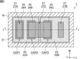
- FIG. 1 is a cross-sectional view illustrating an example of a capacitor according to a first embodiment of the present invention.
- FIG. 2 is a plan view illustrating an example of the capacitor according to the first embodiment of the present invention.
- FIG. 3 shows an equivalent circuit of the capacitor shown in FIGS.
- FIG. 4 is a cross-sectional view illustrating an example of a capacitor according to a second embodiment of the present invention.
- FIG. 5 is a plan view illustrating an example of a capacitor according to a second embodiment of the present invention.
- FIG. 6 shows an equivalent circuit of the capacitor shown in FIGS.
- FIG. 7 is a cross-sectional view showing a schematic example of a capacitor according to a third embodiment of the present invention.
- FIG. 8 is a plan view illustrating an example of a capacitor according to a third embodiment of the present invention.
- FIG. 9 shows an equivalent circuit of the capacitor shown in FIGS.
- FIG. 10 is a cross-sectional view illustrating an example of a capacitor according to a fourth embodiment of the present invention.
- FIG. 11 is a plan view illustrating an example of a capacitor according to a fourth embodiment of the present invention.
- FIG. 12 shows an equivalent circuit of the capacitor shown in FIGS.
- FIG. 13 is a cross-sectional view illustrating an example of a capacitor according to a fifth embodiment of the present invention.
- FIG. 14 is a plan view illustrating an example of a capacitor according to a fifth embodiment of the present invention.
- FIG. 15 shows an equivalent circuit of the capacitor shown in FIGS. FIG.
- FIG. 16 is a cross-sectional view illustrating an example of a capacitor according to a sixth embodiment of the present invention.
- FIG. 17 is a plan view illustrating an example of a capacitor according to a sixth embodiment of the present invention.
- FIG. 18 shows an equivalent circuit of the capacitor shown in FIGS.
- FIG. 19 is a circuit diagram showing a filter circuit according to a comparative example.
- the present invention is not limited to the following configurations, and can be appropriately modified and applied within the scope of the present invention.
- the present invention also includes a combination of two or more of the individual preferred configurations of the present invention described below.
- each embodiment will be referred to simply as the "semiconductor device of the present invention.”
- the shape and arrangement of each component of the semiconductor device of the present invention are not limited to the examples shown in the drawings.
- the semiconductor device of the present invention may be a capacitor itself, or may be a device that includes a capacitor.
- the semiconductor device of the present invention comprises a substrate, N first electrodes (where N is an integer of 2 or more) provided on the substrate, a first dielectric film provided on the N first electrodes, M second electrodes (where M is an integer of 3 or more satisfying M>N) provided on the N first electrodes via the first dielectric film, a first protective layer covering the N first electrodes and the M second electrodes, three or more external electrodes penetrating the first protective layer, and a second protective layer covering the external electrodes excluding two of the three or more external electrodes, at least one second electrode being disposed on each of the first electrodes, and M capacitor elements being constituted by the N first electrodes, the first dielectric film, and the M second electrodes.
- the M capacitor elements are electrically connected in series, and among the M capacitor elements, two capacitor elements having two second electrodes arranged on the same first electrode are electrically connected in series with their first electrodes, and the two external electrodes that are not covered with the second protective layer constitute two terminal electrodes that are electrically connected to two of the M capacitor elements, respectively, and among the M capacitor elements, two capacitor elements having two second electrodes arranged on different first electrodes are electrically connected in series with external electrodes that do not constitute the two terminal electrodes, and the external electrodes that do not constitute the two terminal electrodes are covered with the second protective layer.
- first, second, third, fourth, ... electrodes refer to the electrodes that are present in the first layer (first), second layer (second), third layer (third), fourth layer (fourth), ... of the electrodes that form the capacitor element, counting from the substrate side.
- capacitor element refers to an element (small capacitor) composed of a dielectric film and a pair of electrodes facing each other through the dielectric film
- capacitor refers to the concept of including multiple capacitor elements
- FIG. 1 is a cross-sectional view showing an example of a capacitor according to a first embodiment of the present invention.
- FIG. 2 is a plan view showing an example of a capacitor according to a first embodiment of the present invention.
- FIG. 1 is a cross-sectional view taken along line II of the capacitor shown in FIG. 2.
- FIG. 3 shows an equivalent circuit of the capacitor shown in FIG. 1 and FIG. 2.
- the length direction, width direction, and thickness direction of a capacitor are defined as the directions indicated by arrows L, W, and T, respectively, as shown in Figures 1 and 2.
- the length direction L, width direction W, and thickness direction T are mutually orthogonal.
- the capacitor 1 shown in FIG. 1 and FIG. 2 includes a substrate 10, an insulating film 21 provided on the substrate 10, two first electrodes 22 provided on the insulating film 21, a first dielectric film 23 provided on the two first electrodes, three second electrodes 24 provided on the two first electrodes 22 via the first dielectric film 23, a moisture-resistant film 25 provided on the first dielectric film 23 and the second electrode 24, a first protective layer 26 covering the two first electrodes 22, the three second electrodes 24, and the moisture-resistant film 25, three external electrodes 27 penetrating the first protective layer 26, and a second protective layer 29 covering one of the three external electrodes 27 except for the two external electrodes 27.
- the second electrode 24 includes second electrodes 24A and 24B provided on the first electrode 22A, and a second electrode 24C provided on the first electrode 22B.
- At least one second electrode 24 is disposed on each first electrode 22, and three capacitor elements CAP1, CAP2, and CAP3 are formed from two first electrodes 22, a first dielectric film 23, and three second electrodes 24.
- the three capacitor elements CAP1, CAP2, and CAP3 are electrically connected in series (see FIG. 3).
- two capacitor elements CAP1 and CAP2 having two second electrodes 24A and 24B disposed on the same first electrode 22A are electrically connected in series with their first electrodes 22A, and two capacitor elements CAP1 and CAP2 that are not covered with the second protective layer 29 are electrically connected in series with their first electrodes 22A.
- the two external electrodes 27 constitute two terminal electrodes 27A and 27B electrically connected to two of the three capacitor elements CAP1, CAP2, and CAP3, respectively.
- the two capacitor elements CAP2 and CAP3 having two second electrodes 24B and 24C arranged on different first electrodes 22A and 22B are electrically connected in series with the external electrode 27C that does not constitute the two terminal electrodes 27A and 27B, and the external electrode 27C that does not constitute the two terminal electrodes 27A and 27B is covered with a second protective layer 29.
- the capacitance generated by the variation in thickness of the dielectric film within the wafer surface is C0 ⁇ C0.
- the target capacitance C0/3 can be achieved whether the capacitances C1, C2, and C3 are the same value or a combination of different values.
- the capacitance variation reflecting the film thickness variation of the dielectric film differs for each capacitance, and when different capacitances C1, C2, and C3 are used, the total capacitance variation ⁇ C0/3 becomes large, so it is preferable that the capacitances C1, C2, and C3 are the same capacitance.
- Another effect is that by connecting multiple capacitor elements in series, it is easy to form a low-capacitance capacitor. For example, if one capacitor is formed on one chip with a dielectric film that is 1 ⁇ m thick, the capacitance will be 1 pF. On the other hand, with the above configuration, the electrode area is 1/4 and there are three capacitors in series, making it possible to form a low-capacitance capacitor with a capacitance of 0.1 pF or less.
- the two capacitor elements CAP2 and CAP3 formed by the different first electrodes 22A and 22B are not electrically connected in series to a common second electrode, but are electrically connected in series to the external electrode 27C that penetrates the first protective layer 26, so that it is possible to suppress interference between the capacitor elements CAP2 and CAP3. This interference can be particularly suppressed when the substrate 10 is a semiconductor substrate.
- the substrate 10 is not particularly limited, but is preferably a semiconductor substrate such as a silicon substrate or a gallium arsenide substrate, or an insulating substrate such as glass or alumina.
- the insulating film 21 is provided so as to cover the entirety of one of the main surfaces of the substrate 10.
- the insulating film 21 may be provided so as to cover a portion of one of the main surfaces of the substrate 10, but it must be provided in an area that is larger than the first electrode 22 and overlaps the entire area of the first electrode 22. Note that if the substrate 10 is an insulating substrate such as glass or alumina, the insulating film 21 does not need to be provided.
- the capacitor elements CAP1, CAP2, and CAP3 are electrically insulated from the semiconductor substrate. This makes it possible to reduce the parasitic capacitance components of each of the capacitor elements CAP1, CAP2, and CAP3.
- the material constituting the insulating film 21 is not particularly limited, but preferable examples include SiO2 , SiN, Al2O3 , HfO2 , Ta2O5 , and ZrO2 .
- the first electrode 22 is provided at a position away from the edge of the substrate 10. In other words, the edge of the first electrode 22 is located inside the edge of the substrate 10.
- the material constituting the first electrode 22 is not particularly limited, but is preferably Cu, Ag, Au, Al, Ni, Cr, or Ti, or an alloy containing at least one of these metals.
- the first dielectric film 23 is provided so as to cover the first electrode 22 except for the opening.
- the end of the first dielectric film 23 is also provided on the surface of the insulating film 21 from the end of the first electrode 22 to the end of the substrate 10. The end of the first dielectric film 23 does not have to be provided to the end of the substrate 10.
- the material constituting the first dielectric film 23 is not particularly limited, but preferably includes oxides or nitrides such as SiO2 , SiN , Al2O3 , HfO2 , and Ta2O5 .
- the second electrode 24 is disposed opposite the first electrode 22 with the first dielectric film 23 interposed therebetween. More specifically, the second electrodes 24A and 24B face the first electrode 22A, and the second electrode 24C faces the first electrode 22B.
- the three second electrodes 24 have the same area and the same planar shape. Specifically, the three second electrodes 24 have a rectangular shape with the same dimensions in the length direction L and width direction W.
- the material constituting the second electrode 24 is not particularly limited, but is preferably Cu, Ag, Au, Al, Ni, Cr, or Ti, or an alloy containing at least one of these metals.
- the moisture-resistant film 25 is provided so as to cover the first dielectric film 23 and the second electrode 24 except for the opening.
- the provision of the moisture-resistant film 25 enhances the moisture resistance of the capacitor element, particularly the first dielectric film 23. Note that the moisture-resistant film 25 does not necessarily have to be provided.
- the material constituting the moisture-resistant film 25 is not particularly limited, but preferably includes moisture-resistant materials such as SiO 2 and SiN.
- the first protective layer 26 has openings at positions overlapping the openings of the first dielectric film 23 and moisture-resistant film 25 (openings overlapping the first electrode 22B) and at a position overlapping the opening of the moisture-resistant film 25 (openings overlapping the second electrode 24).
- the provision of the first protective layer 26 protects the capacitor element, and in particular the first dielectric film 23, from moisture.
- the material constituting the first protective layer 26 is not particularly limited, but preferred examples include resin materials such as polyimide resin and resin in solder resist.
- the thickness of the first protective layer 26 is not particularly limited, but is preferably 0.5 ⁇ m or more and 10 ⁇ m or less, and more preferably 1 ⁇ m or more and 5 ⁇ m or less.
- the external electrodes 27 constituting the terminal electrodes 27A and 27B are each electrically connected to the capacitor elements (here, the capacitor elements CAP1 and CAP3) connected in series at both ends of the three capacitor elements CAP1, CAP2, and CAP3. More specifically, the external electrodes 27 constituting the terminal electrodes 27A and 27B are connected to the second electrode 24A and the first electrode 22B, respectively.
- the external electrode 27C which does not constitute the terminal electrodes 27A and 27B, is a connection wiring, and is electrically connected to the capacitor element (here, capacitor element CAP2) excluding the capacitor element connected in series at both ends of the three capacitor elements CAP1, CAP2, and CAP3, and to the other capacitor element (here, capacitor element CAP3). More specifically, the external electrode 27C is connected to the second electrodes 24B and 24C.
- the material constituting the external electrode 27 is not particularly limited, but preferably includes Cu, Ni, Ag, Au, Al, etc.
- the external electrode 27 may have a single-layer structure or a multi-layer structure.
- the outermost surface of the external electrode 27 is preferably made of Au or Sn.
- the external electrode 27 may have, in order from the substrate 10 side, a seed layer 28a, a first plating layer 28b, and a second plating layer 28c, as shown in FIG. 1.
- the seed layer 28a of the external electrode 27 may be, for example, a laminate (Ti/Cu) of a conductive layer made of titanium (Ti) and a conductive layer made of copper (Cu).
- Examples of the material for the first plating layer 28b of the external electrode 27 include nickel (Ni).
- Examples of materials that may be used for the second plating layer 28c of the external electrode 27 include gold (Au) and tin (Sn).
- the materials constituting the three external electrodes 27 may be the same as each other or different from each other.
- the second protective layer 29 has openings so that the terminal electrodes 27A, 27B are exposed.
- the second protective layer 29 insulates the external electrode 27 (external electrode 27C) excluding the terminal electrodes 27A and 27B from the outside. Furthermore, the provision of the second protective layer 29 makes it possible to more effectively protect the capacitor element, and in particular the first dielectric film 23, from moisture.
- the material constituting the second protective layer 29 is not particularly limited, but preferred examples include resin materials such as polyimide resin and resin in solder resist.
- the distance between adjacent capacitor elements is not particularly limited, but is preferably 5 ⁇ m or more and 100 ⁇ m or less, and more preferably 10 ⁇ m or more and 50 ⁇ m or less. By making it 100 ⁇ m or less, the difference in film thickness of the first dielectric film 23 between each capacitor element becomes small, and capacitor elements of the same capacitance can be formed.
- the capacitor 1 shown in Figures 1 and 2 is manufactured, for example, using a method similar to the manufacturing method of a typical MIM capacitor.
- the capacitor according to the second embodiment of the present invention differs from the first embodiment in that at least two of the three second electrodes have different areas.
- FIG. 4 is a cross-sectional view showing an example of a capacitor according to the second embodiment of the present invention.
- FIG. 5 is a plan view showing an example of a capacitor according to the second embodiment of the present invention.
- FIG. 4 is a cross-sectional view taken along line I-I of the capacitor shown in FIG. 5.
- FIG. 6 shows an equivalent circuit of the capacitor shown in FIGS. 4 and 5.
- the capacitor 1 shown in Figures 1 and 2 can reduce capacitance variation, but there is a possibility that the center of capacitance may deviate from the desired value.
- At least two of the three second electrodes 24 have different areas. This makes it possible to adjust the capacitance center. This is because the area of each second electrode 24 can be set so as to cancel out the film thickness distribution of the first dielectric film 23 within the wafer surface.
- each second electrode 24 is composed of a first region 30a having a rectangular planar shape and a second region 30b having a rectangular planar shape protruding from the first region 30a.
- the areas of the first regions 30a of the three second electrodes 24 are the same, while the areas of the second regions 30b of at least two of the three second electrodes 24 are different from each other.
- the areas of all the second electrodes 24 may be different from each other, and the areas of the second regions 30b of all the second electrodes 24 may be different from each other.
- the capacitor 2 shown in Figures 4 and 5 is manufactured using, for example, the method described in Patent Document 2.
- the capacitance center can be adjusted to a desired value.
- the area of the second electrode 24 can be corrected to cancel the film thickness distribution of the first dielectric film 23 within the wafer surface, making it possible to reduce the capacitance distribution. In other words, a capacitor with an adjusted capacitance center and reduced capacitance variation can be realized.
- FIG. 7 is a cross-sectional view showing an example of a capacitor according to the third embodiment of the present invention.
- FIG. 8 is a plan view showing an example of a capacitor according to the third embodiment of the present invention.
- FIG. 7 is a cross-sectional view taken along line I-I of the capacitor shown in FIG. 8.
- FIG. 9 shows an equivalent circuit of the capacitor shown in FIGS. 7 and 8.
- the capacitor 3 shown in Figures 7 and 8 further includes a second dielectric film 31 provided on the three second electrodes 24, and three third electrodes 32 provided on the three second electrodes 24, respectively, via the second dielectric film 31.
- three capacitor elements CAP4, CAP5, and CAP6 are composed of three second electrodes 24, a second dielectric film 31, and three third electrodes 32, and the six capacitor elements CAP1 to CAP6 are electrically connected in series (see Figure 9).
- the number of series connections can be increased, and capacitance variation can be further suppressed.
- the capacitor elements are formed in the thickness direction, the chip can be made smaller.
- At least two of the three third electrodes 32 have different areas. This makes it possible to adjust the center of capacitance. This is because the area of each third electrode 32 can be set so as to cancel out the film thickness distribution of the second dielectric film 31 within the wafer surface.
- each third electrode 32 is composed of a first region 33a having a rectangular planar shape and a second region 33b having a rectangular planar shape protruding from the first region 33a.
- the areas of the first regions 33a of the three third electrodes 32 are the same, while the areas of the second regions 33b of at least two of the three third electrodes 32 are different from each other.
- the areas of all the third electrodes 32 may be different from each other, and the areas of the second regions 33b of all the third electrodes 32 may be different from each other.
- FIG. 8 shows a state in which each third electrode 32 overlaps exactly with the opposing second electrode 24 when viewed from a plane in the thickness direction T, but each third electrode 32 may partially overlap with the opposing second electrode 24 when viewed from a plane in the thickness direction T. Also, each third electrode 32 may be formed within the frame of each second electrode 24.
- the capacitor 3 shown in Figures 7 and 8 is manufactured using, for example, the method described in Patent Document 2.
- the second dielectric film 31 is provided so as to cover the second electrode 24 except for the opening.
- the end of the second dielectric film 31 is also provided on the surface of the first dielectric film 23 between the end of the first electrode 22 and the first dielectric film 23.
- the end of the second dielectric film 31 does not have to be provided to the end of the substrate 10.
- the material constituting the second dielectric film 31 is not particularly limited , but preferably includes oxides or nitrides such as SiO2 , SiN, Al2O3 , HfO2 , and Ta2O5 .
- the third electrode 32 is disposed opposite the second electrode 24 with the second dielectric film 31 interposed therebetween. More specifically, the third electrode 32 includes a third electrode 32A opposite the second electrode 24A, a third electrode 32B opposite the second electrode 24B, and a third electrode 32C opposite the second electrode 24C.
- the material constituting the third electrode 32 is not particularly limited, but is preferably Cu, Ag, Au, Al, Ni, Cr, or Ti, or an alloy containing at least one of these metals.
- the external electrodes 27 constituting the terminal electrodes 27A and 27B are each electrically connected to one of the six capacitor elements CAP1 to CAP6 (capacitor elements CAP4 and CAP3 in this example) that are connected in series to both ends. More specifically, the external electrodes 27 constituting the terminal electrodes 27A and 27B are each connected to the third electrode 32A and the first electrode 22B.
- the external electrode 27C which does not constitute the terminal electrodes 27A and 27B, is electrically connected to two of the six capacitor elements CAP1 to CAP6 (here, the capacitor elements CAP5 and CAP6) excluding the capacitor elements connected in series at both ends. More specifically, the external electrode 27C is connected to the third electrodes 32B and 32C.
- FIG. 10 is a cross-sectional view showing an example of a capacitor according to the fourth embodiment of the present invention.
- FIG. 11 is a plan view showing an example of a capacitor according to the fourth embodiment of the present invention.
- FIG. 10 is a cross-sectional view taken along line II of the capacitor shown in FIG. 11.
- FIG. 12 shows an equivalent circuit of the capacitor shown in FIGS. 10 and 11.
- the capacitor 4 shown in Figures 10 and 11 further includes a third dielectric film 34 provided on the three third electrodes 32, and three fourth electrodes 35 provided on the three third electrodes 32, respectively, via the third dielectric film 34.
- three capacitor elements CAP7, CAP8, and CAP9 are composed of three third electrodes 32, a third dielectric film 34, and three fourth electrodes 35, and the nine capacitor elements CAP1 to CAP9 are electrically connected in series (see FIG. 12).
- the number of series connections can be increased, and capacitance variation can be further suppressed.
- the capacitor elements are formed in the thickness direction, the chip can be made smaller.
- At least two of the three fourth electrodes 35 have different areas. This makes it possible to adjust the capacitance center. This is because the area of each fourth electrode 35 can be set so as to cancel out the film thickness distribution of the third dielectric film 34 within the wafer surface.
- each fourth electrode 35 is composed of a first region 36a having a rectangular planar shape and a second region 36b having a rectangular planar shape protruding from the first region 36a.
- the areas of the first regions 36a of the three fourth electrodes 35 are the same, while the areas of the second regions 36b of at least two of the three fourth electrodes 35 are different from each other.
- the areas of all the fourth electrodes 35 may be different from each other, and the areas of the second regions 36b of all the fourth electrodes 35 may be different from each other.
- FIG. 11 shows a state in which each fourth electrode 35 overlaps the opposing third electrode 32 perfectly, but in plan view from the thickness direction T, each fourth electrode 35 may partially overlap the opposing third electrode 32. Also, in plan view from the thickness direction T, FIG. 11 shows a state in which each third electrode 32 overlaps the opposing second electrode 24 perfectly, but in plan view from the thickness direction T, each third electrode 32 may partially overlap the opposing second electrode 24. Also, each fourth electrode 35 may be formed within the frame of each third electrode 32, and each third electrode 32 may be formed within the frame of each second electrode 24.
- the capacitor 4 shown in Figures 10 and 11 is manufactured using, for example, the method described in Patent Document 2.
- the third dielectric film 34 is provided so as to cover the third electrode 32 except for the opening.
- the end of the third dielectric film 34 is also provided on the surface of the second dielectric film 31 between the end of the first electrode 22 and the second dielectric film 31.
- the end of the third dielectric film 34 does not have to be provided to the end of the substrate 10.
- the material constituting the third dielectric film 34 is not particularly limited, but preferably includes oxides or nitrides such as SiO2 , SiN, Al2O3 , HfO2 , and Ta2O5 .
- the fourth electrode 35 is disposed opposite the third electrode 32 with the third dielectric film 34 interposed therebetween. More specifically, the fourth electrode 35 includes a fourth electrode 35A opposite the third electrode 32A, a fourth electrode 35B opposite the third electrode 32B, and a fourth electrode 35C opposite the third electrode 32C.
- the material constituting the fourth electrode 35 is not particularly limited, but is preferably Cu, Ag, Au, Al, Ni, Cr, or Ti, or an alloy containing at least one of these metals.
- the external electrodes 27 constituting the terminal electrodes 27A and 27B are each electrically connected to the capacitor elements (here, the capacitor elements CAP7 and CAP3) connected in series to both ends of the nine capacitor elements CAP1 to CAP9. More specifically, the external electrodes 27 constituting the terminal electrodes 27A and 27B are connected to the fourth electrode 35A and the first electrode 22B, respectively.
- the external electrode 27C which does not constitute the terminal electrodes 27A and 27B, is electrically connected to two of the nine capacitor elements CAP1 to CAP9 (here, capacitor elements CAP8 and CAP9) excluding the capacitor elements connected in series at both ends. More specifically, the external electrode 27C is connected to the fourth electrodes 35B and 35C.
- the capacitor according to the fifth embodiment of the present invention differs from the second embodiment in that an element isolation is provided between three capacitor elements within a semiconductor substrate.
- FIG. 13 is a cross-sectional view showing an example of a capacitor according to the fifth embodiment of the present invention.
- FIG. 14 is a plan view showing an example of a capacitor according to the fifth embodiment of the present invention.
- FIG. 13 is a cross-sectional view taken along line II of the capacitor shown in FIG. 14.
- FIG. 15 shows an equivalent circuit of the capacitor shown in FIGS. 13 and 14.
- the substrate 10 is a semiconductor substrate, and element isolation 37 is provided in the semiconductor substrate between the three capacitor elements CAP1, CAP2, and CAP3.
- the element isolation 37 has a structure in which a cavity is formed in a semiconductor substrate and an SiO 2 film is embedded therein (STI: Shallow Trench Isolation).
- STI Shallow Trench Isolation
- the element isolation 37 is provided at least between adjacent capacitor elements (here, between capacitor elements CAP1 and CAP2 and between capacitor elements CAP2 and CAP3), and is preferably provided so as to surround each of the capacitor elements CAP1, CAP2, and CAP3. Furthermore, the element isolation 37 is preferably arranged so as to overlap the peripheral portion of the first electrode 22 and border the peripheral portion.
- the capacitor according to the sixth embodiment of the present invention differs from the fifth embodiment in that the material for element isolation is different.
- FIG. 16 is a cross-sectional view showing an example of a capacitor according to the sixth embodiment of the present invention.
- FIG. 17 is a plan view showing an example of a capacitor according to the sixth embodiment of the present invention.
- FIG. 16 is a cross-sectional view taken along line II of the capacitor shown in FIG. 17.
- FIG. 18 shows an equivalent circuit of the capacitor shown in FIGS. 16 and 17.
- the substrate 10 is an n-type semiconductor substrate
- the element isolation 37 has a structure in which a p+ active layer is formed in an n-type semiconductor substrate.
- Such element isolation 37 can be formed, for example, by injecting a high concentration of p-type impurities into an n-type semiconductor substrate by ion implantation.
- This embodiment also reduces the current flowing through the semiconductor substrate between adjacent capacitor elements, making it possible to reduce the mutual interference between adjacent capacitor elements. As a result, the accuracy of the center capacitance value and capacitance variation of the capacitor 6 can be improved.
- the semiconductor device of the present invention is not limited to the above-described embodiment, and various applications and modifications can be made within the scope of the present invention with respect to the configuration and manufacturing conditions of the semiconductor device such as a capacitor.
- a fourth second electrode may be provided on the first electrode 22B via the first dielectric film 23, and the terminal electrode 27B may be connected to the second electrode.
- a fourth second electrode may be provided on the first electrode 22B via the first dielectric film 23, and a fourth third electrode may be provided on the second electrode via the second dielectric film 31, and the terminal electrode 27B may be connected to the third electrode.
- a fourth second electrode may be provided on the first electrode 22B via the first dielectric film 23
- a fourth third electrode may be provided on the second electrode via the second dielectric film 31
- a fourth fourth electrode may be provided on the third electrode via the third dielectric film 34
- the terminal electrode 27B may be connected to the fourth electrode.
- N is not particularly limited as long as it is an integer of 2 or more, and may be, for example, 3.
- a third first electrode is provided between the two first electrodes 22A and 22B, and a fourth and fifth second electrode is provided on the first electrode via the first dielectric film 23 to form a fourth and fifth capacitor element (a total of five capacitor elements connected in series), and the fourth capacitor element and capacitor element CAP2 are electrically connected in series with external electrodes that do not constitute the terminal electrodes 27A and 27B, and the fifth capacitor element and capacitor element CAP3 are electrically connected in series with external electrodes that do not constitute the terminal electrodes 27A and 27B.
- N first electrodes (where N is an integer of 2 or more) provided on the substrate; a first dielectric film provided on the N first electrodes; M second electrodes (where M is an integer of 3 or more satisfying M>N) provided on the N first electrodes via the first dielectric film; a first protective layer covering the N first electrodes and the M second electrodes; Three or more external electrodes penetrating the first protective layer; a second protective layer that covers the external electrodes excluding two of the three or more external electrodes; At least one second electrode is disposed on each of the first electrodes; the N first electrodes, the first dielectric film, and the M second electrodes constitute M capacitor elements; The M capacitor elements are electrically connected in series, Among the M capacitor elements, two capacitor elements having two second electrodes arranged on the same first electrode are electrically connected in series at their first electrodes; the two external electrodes not covered with the second protective layer constitute two terminal electrodes electrically connected to two of the M capacitor elements, respectively; Among the M capacitor elements, two capacitor elements each
- ⁇ 2> The semiconductor device according to ⁇ 1>, wherein at least two of the M second electrodes have areas different from each other.
- ⁇ 3> a second dielectric film provided on the M second electrodes;
- ⁇ 4> The semiconductor device according to ⁇ 3>, wherein at least two of the M third electrodes have areas different from each other.
- ⁇ 5> a third dielectric film provided on the M third electrodes;
- ⁇ 6> 6 The semiconductor device according to claim 5, wherein at least two of said M fourth electrodes have areas different from each other.
- the substrate is a semiconductor substrate
Landscapes
- Engineering & Computer Science (AREA)
- Power Engineering (AREA)
- Microelectronics & Electronic Packaging (AREA)
- Manufacturing & Machinery (AREA)
- Semiconductor Integrated Circuits (AREA)
Priority Applications (3)
| Application Number | Priority Date | Filing Date | Title |
|---|---|---|---|
| JP2025526021A JPWO2024252870A1 (enExample) | 2023-06-07 | 2024-05-15 | |
| CN202480037187.4A CN121312282A (zh) | 2023-06-07 | 2024-05-15 | 半导体装置 |
| US19/400,643 US20260082686A1 (en) | 2023-06-07 | 2025-11-25 | Semiconductor device |
Applications Claiming Priority (2)
| Application Number | Priority Date | Filing Date | Title |
|---|---|---|---|
| JP2023094199 | 2023-06-07 | ||
| JP2023-094199 | 2023-06-07 |
Related Child Applications (1)
| Application Number | Title | Priority Date | Filing Date |
|---|---|---|---|
| US19/400,643 Continuation US20260082686A1 (en) | 2023-06-07 | 2025-11-25 | Semiconductor device |
Publications (1)
| Publication Number | Publication Date |
|---|---|
| WO2024252870A1 true WO2024252870A1 (ja) | 2024-12-12 |
Family
ID=93795339
Family Applications (1)
| Application Number | Title | Priority Date | Filing Date |
|---|---|---|---|
| PCT/JP2024/017949 Pending WO2024252870A1 (ja) | 2023-06-07 | 2024-05-15 | 半導体装置 |
Country Status (4)
| Country | Link |
|---|---|
| US (1) | US20260082686A1 (enExample) |
| JP (1) | JPWO2024252870A1 (enExample) |
| CN (1) | CN121312282A (enExample) |
| WO (1) | WO2024252870A1 (enExample) |
Citations (9)
| Publication number | Priority date | Publication date | Assignee | Title |
|---|---|---|---|---|
| JP2005032981A (ja) * | 2003-07-14 | 2005-02-03 | Shinko Electric Ind Co Ltd | キャパシタ装置及びその製造方法 |
| JP2007335842A (ja) * | 2006-05-19 | 2007-12-27 | Casio Comput Co Ltd | チップ型電子部品 |
| JP2012038818A (ja) * | 2010-08-04 | 2012-02-23 | Toshiba Corp | 半導体装置 |
| US20150102459A1 (en) * | 2013-10-11 | 2015-04-16 | Taiwan Semiconductor Manufacturing Company, Ltd. | Metal Insulator Metal Capacitor and Method for Making the Same |
| WO2016136411A1 (ja) * | 2015-02-27 | 2016-09-01 | 株式会社村田製作所 | キャパシタおよび電子機器 |
| WO2016136564A1 (ja) * | 2015-02-27 | 2016-09-01 | 株式会社村田製作所 | キャパシタ |
| US20170178810A1 (en) * | 2015-12-21 | 2017-06-22 | Qualcomm Incorporated | Mim capacitor and method of making the same |
| WO2017159283A1 (ja) * | 2016-03-18 | 2017-09-21 | 株式会社村田製作所 | 容量素子 |
| WO2020012691A1 (ja) * | 2018-07-11 | 2020-01-16 | 株式会社村田製作所 | 容量素子 |
-
2024
- 2024-05-15 CN CN202480037187.4A patent/CN121312282A/zh active Pending
- 2024-05-15 JP JP2025526021A patent/JPWO2024252870A1/ja active Pending
- 2024-05-15 WO PCT/JP2024/017949 patent/WO2024252870A1/ja active Pending
-
2025
- 2025-11-25 US US19/400,643 patent/US20260082686A1/en active Pending
Patent Citations (9)
| Publication number | Priority date | Publication date | Assignee | Title |
|---|---|---|---|---|
| JP2005032981A (ja) * | 2003-07-14 | 2005-02-03 | Shinko Electric Ind Co Ltd | キャパシタ装置及びその製造方法 |
| JP2007335842A (ja) * | 2006-05-19 | 2007-12-27 | Casio Comput Co Ltd | チップ型電子部品 |
| JP2012038818A (ja) * | 2010-08-04 | 2012-02-23 | Toshiba Corp | 半導体装置 |
| US20150102459A1 (en) * | 2013-10-11 | 2015-04-16 | Taiwan Semiconductor Manufacturing Company, Ltd. | Metal Insulator Metal Capacitor and Method for Making the Same |
| WO2016136411A1 (ja) * | 2015-02-27 | 2016-09-01 | 株式会社村田製作所 | キャパシタおよび電子機器 |
| WO2016136564A1 (ja) * | 2015-02-27 | 2016-09-01 | 株式会社村田製作所 | キャパシタ |
| US20170178810A1 (en) * | 2015-12-21 | 2017-06-22 | Qualcomm Incorporated | Mim capacitor and method of making the same |
| WO2017159283A1 (ja) * | 2016-03-18 | 2017-09-21 | 株式会社村田製作所 | 容量素子 |
| WO2020012691A1 (ja) * | 2018-07-11 | 2020-01-16 | 株式会社村田製作所 | 容量素子 |
Also Published As
| Publication number | Publication date |
|---|---|
| US20260082686A1 (en) | 2026-03-19 |
| CN121312282A (zh) | 2026-01-09 |
| JPWO2024252870A1 (enExample) | 2024-12-12 |
Similar Documents
| Publication | Publication Date | Title |
|---|---|---|
| US8514539B2 (en) | Composite electronic device | |
| CN112103284B (zh) | 芯片元件 | |
| JP4500840B2 (ja) | 積層型バラン及び混成集積回路モジュール並びに積層基板 | |
| US8422190B2 (en) | Composite electronic device, manufacturing method thereof, and connection structure of composite electronic device | |
| US20070222052A1 (en) | Wiring structure, multilayer wiring board, and electronic device | |
| EP3098900B1 (en) | Passive component | |
| JP6693080B2 (ja) | 積層型フィルタ | |
| WO2014132939A1 (ja) | 半導体装置 | |
| KR100475477B1 (ko) | 인덕턴스 소자 및 반도체 장치 | |
| TW201739033A (zh) | 電子零件 | |
| CN108023152B (zh) | 定向耦合器 | |
| JP4518013B2 (ja) | 電子部品 | |
| US20190244761A1 (en) | Capacitor | |
| WO2024252870A1 (ja) | 半導体装置 | |
| JP3198252B2 (ja) | 分波器及びその製造方法 | |
| JP7647880B2 (ja) | 半導体装置 | |
| US10276912B2 (en) | Directional coupler | |
| US20230198169A1 (en) | Transmission component and semiconductor device | |
| US3908186A (en) | Packaged semiconductor device for microwave use | |
| JPH09162692A (ja) | 弾性表面波装置 | |
| US20250037919A1 (en) | Electronic component | |
| US20250246349A1 (en) | Coil component | |
| US20260040589A1 (en) | Electronic component | |
| US20250293656A1 (en) | Filter circuit | |
| US20260039005A1 (en) | Electronic component |
Legal Events
| Date | Code | Title | Description |
|---|---|---|---|
| 121 | Ep: the epo has been informed by wipo that ep was designated in this application |
Ref document number: 24819107 Country of ref document: EP Kind code of ref document: A1 |
|
| ENP | Entry into the national phase |
Ref document number: 2025526021 Country of ref document: JP Kind code of ref document: A |
|
| WWE | Wipo information: entry into national phase |
Ref document number: 2025526021 Country of ref document: JP |
|
| NENP | Non-entry into the national phase |
Ref country code: DE |