WO2024247740A1 - 基板処理方法及び基板処理システム - Google Patents
基板処理方法及び基板処理システム Download PDFInfo
- Publication number
- WO2024247740A1 WO2024247740A1 PCT/JP2024/018100 JP2024018100W WO2024247740A1 WO 2024247740 A1 WO2024247740 A1 WO 2024247740A1 JP 2024018100 W JP2024018100 W JP 2024018100W WO 2024247740 A1 WO2024247740 A1 WO 2024247740A1
- Authority
- WO
- WIPO (PCT)
- Prior art keywords
- peripheral
- substrate
- region
- wafer
- bonding
- Prior art date
- Legal status (The legal status is an assumption and is not a legal conclusion. Google has not performed a legal analysis and makes no representation as to the accuracy of the status listed.)
- Ceased
Links
Images




Classifications
-
- H—ELECTRICITY
- H10—SEMICONDUCTOR DEVICES; ELECTRIC SOLID-STATE DEVICES NOT OTHERWISE PROVIDED FOR
- H10P—GENERIC PROCESSES OR APPARATUS FOR THE MANUFACTURE OR TREATMENT OF DEVICES COVERED BY CLASS H10
- H10P54/00—Cutting or separating of wafers, substrates or parts of devices
- H10P54/30—Cutting or separating of wafers, substrates or parts of devices by forming weakened zones for subsequent cutting or separating, e.g. by laser treatment or by ion implantation
-
- B—PERFORMING OPERATIONS; TRANSPORTING
- B23—MACHINE TOOLS; METAL-WORKING NOT OTHERWISE PROVIDED FOR
- B23K—SOLDERING OR UNSOLDERING; WELDING; CLADDING OR PLATING BY SOLDERING OR WELDING; CUTTING BY APPLYING HEAT LOCALLY, e.g. FLAME CUTTING; WORKING BY LASER BEAM
- B23K26/00—Working by laser beam, e.g. welding, cutting or boring
- B23K26/50—Working by transmitting the laser beam through or within the workpiece
- B23K26/53—Working by transmitting the laser beam through or within the workpiece for modifying or reforming the material inside the workpiece, e.g. for producing break initiation cracks
-
- H—ELECTRICITY
- H10—SEMICONDUCTOR DEVICES; ELECTRIC SOLID-STATE DEVICES NOT OTHERWISE PROVIDED FOR
- H10P—GENERIC PROCESSES OR APPARATUS FOR THE MANUFACTURE OR TREATMENT OF DEVICES COVERED BY CLASS H10
- H10P52/00—Grinding, lapping or polishing of wafers, substrates or parts of devices
-
- H—ELECTRICITY
- H10—SEMICONDUCTOR DEVICES; ELECTRIC SOLID-STATE DEVICES NOT OTHERWISE PROVIDED FOR
- H10P—GENERIC PROCESSES OR APPARATUS FOR THE MANUFACTURE OR TREATMENT OF DEVICES COVERED BY CLASS H10
- H10P72/00—Handling or holding of wafers, substrates or devices during manufacture or treatment thereof
- H10P72/04—Apparatus for manufacture or treatment
- H10P72/0428—Apparatus for mechanical treatment or grinding or cutting
Definitions
- This disclosure relates to a substrate processing method and a substrate processing system.
- Patent Document 1 discloses a method for processing a laminated substrate in which a first substrate and a second substrate are bonded together.
- the processing method includes cutting the peripheral portion of the first substrate from above to a thickness less than the total thickness of the first substrate so as to leave a cutting remainder of a desired thickness, and irradiating the cutting remainder at the peripheral portion of the first substrate with laser light to remove the cutting remainder.
- the technology disclosed herein appropriately removes the peripheral portion of the first substrate to be removed in a polymerized substrate in which a first substrate and a second substrate are bonded together.
- One aspect of the present disclosure is a substrate processing method for processing a laminated substrate in which a first substrate and a second substrate are bonded together, the method including: forming a first peripheral modified region inside the first substrate along a boundary between a peripheral portion and a central portion of the first substrate to be removed; forming a second peripheral modified portion radially inside the first substrate at least radially outward from the first peripheral modified region; forming a reduced bonding strength region in which bonding strength is reduced in the bonding region between the first substrate and the second substrate radially outward from the first peripheral modified region by forming the second peripheral modified portion; and removing the peripheral portion based on the first peripheral modified region and the reduced bonding strength region.
- the peripheral portion of the first substrate to be removed can be appropriately removed.
- FIG. 2 is an explanatory diagram of a laminated wafer to be processed.
- 1 is a plan view showing an outline of a configuration of a wafer processing system;
- FIG. 2 is a plan view showing the outline of the configuration of the reformer.
- FIG. 2 is a side view showing the outline of the configuration of a reformer.
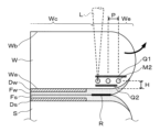
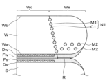
- 1A to 1C are explanatory diagrams showing the formation of a first peripheral modified region and a second peripheral modified portion in wafer processing.
- 11A to 11C are explanatory views showing how a second peripheral modified region is formed in wafer processing.
- 1A-1C are diagrams illustrating the formation of a first peripheral modified region during wafer processing.
- 1A to 1C are explanatory views showing a state in which a peripheral portion is removed in wafer processing.
- 10A to 10C are explanatory diagrams showing how a first peripheral modified region is formed in another embodiment.
- a first wafer which is a semiconductor substrate (hereafter referred to as a "wafer") having a number of electronic circuits and other devices formed on its surface, is bonded to a second wafer to form a laminated wafer, in which the first wafer is thinned.
- a process known as edge trimming is performed to remove the peripheral portion of the first wafer.
- the edge trim of the first wafer is performed, for example, by the processing method disclosed in Patent Document 1.
- the peripheral portion of the first substrate is cut from above, and then the remaining cut portion on the peripheral portion of the first substrate is irradiated with laser light, and the remaining cut portion is removed by laser ablation.
- removing the peripheral portion in two stages like this, especially laser ablation, is time-consuming, and there is room for improvement in conventional edge trimming.
- a laminated wafer T which is a laminated substrate formed by bonding a first wafer W as a first substrate and a second wafer S as a second substrate, as shown in FIG. 1.
- the surface of the first wafer W that is bonded to the second wafer S is referred to as the front surface Wa
- the surface opposite the front surface Wa is referred to as the back surface Wb.
- the surface of the second wafer S that is bonded to the first wafer W is referred to as the front surface Sa
- the surface opposite the front surface Sa is referred to as the back surface Sb.
- the first wafer W is a semiconductor wafer such as a silicon substrate, and at least one film is formed on the front surface Wa side by lamination.
- the film formed on the front surface Wa side is referred to as the "first laminated film".
- the first laminated film includes a device layer Dw and a bonding film Fw.
- the device layer Dw includes a plurality of devices.
- the bonding film Fw for example, an oxide film (THOX film, SiO 2 film, TEOS film), a SiC film, a SiCN film, or an adhesive is used.
- the first wafer W is bonded to the second wafer S via the bonding film Fw.
- peripheral portion We of the first wafer W is chamfered, and the cross section of the peripheral portion We becomes thinner toward its tip.
- the peripheral portion We is a portion to be removed in the edge trim described later, and is, for example, in the range of 0.5 mm to 3 mm in the radial direction from the outer end of the first wafer W.
- a region of the first wafer W that is radially inward of the peripheral edge portion We to be removed may be referred to as a central portion Wc.
- the second wafer S has, for example, the same configuration as the first wafer W. That is, a device layer Ds and a bonding film Fs are formed as a second laminated film on the surface Sa side, and the peripheral portion is chamfered. Note that the second wafer S does not have to be a device wafer on which a device layer Ds is formed, and may be, for example, a support wafer that supports the first wafer W. In such a case, the second wafer S functions as a protective material that protects the device layer Dw of the first wafer W.
- each layer between the first wafer W and the second wafer S is referred to as a bonding region. That is, in this embodiment, the surface Wa, the area between the device layer Dw and the bonding film Fw, the area between the bonding film Fw and the bonding film Fs, the area between the bonding film Fs and the device layer Ds, and the surface Sa are referred to as bonding regions.
- the device layers Dw, Ds and bonding films Fw, Fs are formed as the first and second laminated films on the surfaces Wa, Sa of the first wafer W and the second wafer S, respectively.
- the types and number of layers of the first and second laminated films are not limited to this.
- the wafer processing system 1 has a configuration in which a loading/unloading station 2 and a processing station 3 are integrally connected.
- a loading/unloading station 2 for example, a cassette C capable of housing multiple polymerized wafers T is loaded and unloaded between the loading/unloading station 2 and the outside.
- the processing station 3 is equipped with various processing devices that perform the desired processing on the polymerized wafers T.
- the loading/unloading station 2 is provided with a cassette mounting table 10 on which a cassette C capable of storing multiple overlapping wafers T is mounted.
- a wafer transport device 20 is provided adjacent to the cassette mounting table 10 on the positive X-axis side of the cassette mounting table 10.
- the wafer transport device 20 moves on a transport path 21 extending in the Y-axis direction, and is configured to be able to transport overlapping wafers T between the cassette C on the cassette mounting table 10 and a transition device 30 described below.
- the loading/unloading station 2 is provided with a transition device 30 adjacent to the wafer transport device 20 on the positive X-axis side of the wafer transport device 20 for transferring the laminated wafer T between the processing station 3 and the wafer transport device 20.
- the modification device 50 irradiates the inside of the first wafer W with a modification laser beam (e.g., a YAG laser or a fiber laser) to form a peripheral modification region and a bonding strength reduction region that serve as a base point for peeling off the peripheral portion We.
- a modification laser beam e.g., a YAG laser or a fiber laser
- the modification device 50 also has a control device 51, which will be described later.
- a laser head 110 is provided above the chuck 100.
- the laser head 110 has a lens 111.
- the lens 111 is a cylindrical member provided on the underside of the laser head 110, and irradiates laser light into the inside of the laminated wafer T held by the chuck 100, more specifically, into the inside of the first wafer W.
- an imaging mechanism 120 is provided above the chuck 100, on the Y-axis positive side of the laser head 110.
- the imaging mechanism 120 has at least one camera. The image captured by the camera is output to the control device 51 or the control device 80 described below.
- the modification device 50 determines the position of the overlapped wafer T on the chuck 100 based on the image obtained by the imaging mechanism 120, and based on this, aligns the overlapped wafer T and determines the irradiation position of the laser light.
- the imaging mechanism 120 is configured to be freely raised and lowered by a lifting mechanism 121, and is further configured to be freely moved in the Y-axis direction by a moving mechanism 122.
- the moving mechanism 122 is supported by a support column 116.
- the edge removal device 60 shown in FIG. 2 removes the edge portion We of the first wafer W, i.e., performs edge trimming, using the edge modification area and the bonding strength reduction area formed by the modification device 50 as base points.
- the edge trimming method can be selected arbitrarily.
- the edge removal device 60 may insert a wedge-shaped blade between the first wafer W and the second wafer S.
- an air blow or water jet may be sprayed toward the edge portion We to apply an impact to the edge portion We.
- ultrasonic waves may be applied to the edge portion We to apply an impact to the edge portion We.
- the edge portion We may be physically moved in a direction away from the center portion Wc.
- the cleaning device 70 performs a cleaning process on the first wafer W and the second wafer S after the edge trimming by the edge removal device 60, and removes particles from these wafers.
- the cleaning method can be selected arbitrarily.
- the above-described wafer processing system 1 is provided with a control device 51 and at least one control device 80.
- the control device 51 individually controls the operation of the modification device 50.
- the control device 80 is responsible for overall control of a series of wafer processes in the wafer processing system 1.
- the control device 51 and the control device 80 may each include a processing unit, a storage unit, and a communication interface.
- the control device 51 and the control device 80 are each realized, for example, by a computer.
- the processing unit may be configured to read a program that provides logic or routines that enable various control operations to be performed from the storage unit, and to perform various control operations by executing the read program.
- This program may be stored in the storage unit in advance, or may be acquired via a medium when necessary.
- the acquired program is stored in the storage unit, and is read from the storage unit by the processing unit and executed.
- the medium may be various storage media that are readable by a computer, or may be a communication line connected to the communication interface.
- the storage medium may be temporary or non-temporary.
- control device 51 is installed separately from the reformer 50, but the control device 51 may be configured integrally with the control device 80. In other words, the operation of the reformer 50 may be controlled by the control device 80.
- the first wafer W and the second wafer S are bonded together outside the wafer processing system 1 before being processed in the wafer processing system 1 to form a laminated wafer T.
- a process for thinning the central portion Wc of the first wafer W is performed outside the wafer processing system 1.
- the process for thinning the first wafer W is optional.
- a thinning device for thinning the central portion Wc of the first wafer W such as a grinding device (not shown), may be provided outside the wafer processing system 1 as in this embodiment, or may be installed in the wafer processing system 1.
- a cassette C containing multiple polymerized wafers T is placed on the cassette placement table 10 of the loading/unloading station 2.
- the polymerized wafers T in the cassette C are removed by the wafer transfer device 20 and transferred to the modification device 50 via the transition device 30 and the wafer transfer device 40.
- a modification laser beam L is irradiated onto the inside of the first wafer W, and a first peripheral modified region M1 and a second peripheral modified region M2 are formed in the circumferential direction in a plan view.
- the first peripheral modified region M1 is formed.
- the second peripheral modified portion M2 may be formed from the radially outer side to the inner side, or from the radially inner side to the outer side.
- the second peripheral modified region M2 is formed near the surface Wa of the first wafer W. Specifically, the distance H in the thickness direction between the second peripheral modified region M2 and the surface Wa is, for example, within 20 ⁇ m.
- adjacent second peripheral modified regions M2 are not connected to each other. In other words, cracks from the second peripheral modified regions M2 do not reach adjacent second peripheral modified regions M2.
- the spacing of the laser light L i.e., the lower limit value of the spacing P of the second peripheral modified regions M2 is the spacing at which cracks do not connect between adjacent second peripheral modified regions M2
- the upper limit value of the spacing P is the spacing at which a bonding strength reduction region R described below can be formed.
- the spacing P is, for example, 30 ⁇ m to 80 ⁇ m.
- the second peripheral modified region M2 expands, causing compressive stress to act, and tensile stress to act on the region Q1 above the second peripheral modified region M2 and the region Q2 below the second peripheral modified region M2.
- tensile stress is accumulated in these regions Q1 and Q2, and tensile stress acts on the surface Wa of the first wafer W.
- compressive stress acts on the upper portion of the first wafer W (the portion above the second peripheral modified region M2) such that the upper portion of the first wafer W tends to warp diagonally upward so that the peripheral region We peels off (arrow in Figure 6).
- the bonding region of the first laminated film and the second laminated film i.e., the bonding region of the bonding film Fw and the bonding film Fs
- the bonding region of the bonding film Fw and the bonding film Fs is the most susceptible to peeling because an unbonded region is formed radially outside this bonding region.
- tensile stress acts on the bonding region of the bonding film Fw and the bonding film Fs in response to the compressive stress (warping) of the upper part of the first wafer W described above, reducing the bonding strength of the bonding region and forming a region of reduced bonding strength R.
- This region of reduced bonding strength R extends between the first peripheral modified region N1 described below and the outer edge.
- the bonding strength reduced region R is unlikely to be formed.
- the bonding strength is reduced in the region formed by the second peripheral modified region M2 and the crack, and the peripheral region is removed from this region as a base point.
- the bonding strength reduced region R is more likely to be formed outside the first wafer W, and the bonding strength reduced region R is removed from the base point of the peripheral region We.
- the second peripheral modification region M2 is formed near the surface Wa of the first wafer W, so that the tensile stress acting on the surface Wa of the first wafer W becomes large, making it even easier for the bonding strength reduction region R to form.
- the bonding strength reduction region R is formed so as to extend radially outward from the first peripheral modified region N1.
- the inside of the first wafer W is irradiated with laser light L along the boundary between the peripheral portion We and the central portion Wc of the first wafer W to form a first peripheral modified portion M1.
- the boundary between the peripheral portion We and the central portion Wc is, for example, a boundary extending in the thickness direction of the first wafer W.
- a first crack C1 extends from the first peripheral modified portion M1 along the boundary between the peripheral portion We and the central portion Wc.
- the first crack C1 extends to the bonding region of the bonding film Fw and the bonding film Fs.
- a first peripheral modified region N1 including the first peripheral modified portion M1 and the first crack C1 is formed.
- the first peripheral modified region N1 extends between the back surface Wb of the first wafer W and the bonding region of the bonding film Fw and the bonding film Fs.
- the compressive stress in the upper portion of the first wafer W is released, and the tensile stress in the bonding strength reduction region R is released.
- the tensile stress is released, for example, from the radially outer side toward the inner side (toward the first peripheral modified region N1).
- the bonding film Fw and the bonding film Fs peel off.
- the peeling in the bonding strength reduction region R progresses to the first peripheral modified region N1, and the bonding strength reduction region R and the first peripheral modified region N1 are connected.
- the first peripheral modified region N1 and the bonding strength reduction region R become the base point when removing the peripheral portion We.
- the laminated wafer T with the first peripheral modified region N1 and the bonding strength reduced region R formed thereon is then transported by the wafer transport device 40 to the peripheral removal device 60.
- a blade B is inserted between the first wafer W and the second wafer S as shown in FIG. 8, and the peripheral portion We is removed from the first wafer W.
- the peripheral portion We is peeled off and removed from the central portion Wc of the first wafer W, using the first peripheral modified region N1 and the bonding strength reduced region R as base points.
- the laminated wafer T from which the peripheral portion We of the first wafer W has been removed is then transported by the wafer transport device 40 to the cleaning device 70.
- the cleaning device 70 the first wafer W from which the peripheral portion We has been removed and/or the second wafer S are cleaned.
- the laminated wafer T which has been subjected to all the processes, is transferred by the wafer transfer device 20 to the cassette C on the cassette mounting table 10 via the transition device 30. This completes the series of wafer processing steps in the wafer processing system 1.
- the second peripheral modified portion M2 is formed, and then the first peripheral modified region N1 (first peripheral modified portion M1) is formed, but the order in which the second peripheral modified portion M2 and the first peripheral modified region N1 are formed is not limited to this.
- the second peripheral modified portion M2 may be formed after the first peripheral modified region N1 is formed. Even in such a case, by not connecting adjacent second peripheral modified portions M2 to each other, it is possible to enjoy the effect of performing the above-mentioned edge trim appropriately and efficiently.
- the second peripheral modification portion M2 is formed radially outward of the first peripheral modification region N1, but in addition to this, it may also be formed radially inward of the first peripheral modification region N1. Even in such a case, it is possible to form a bonding strength reduction region R and appropriately and efficiently remove the peripheral portion We.
- the second peripheral modified portion M2 is formed near the surface Wa of the first wafer W. For this reason, for example, if the second peripheral modified portion M2 is formed above the thinning surface (the surface to be thinned) when thinning the central portion Wc of the first wafer W, there is a risk that the second peripheral modified portion M2 will remain in the central portion Wc of the first wafer W after thinning. For this reason, it is preferable that the second peripheral modified portion M2 is formed radially outward of the first peripheral modified region N1.
- the first peripheral modified region N1 extends from the back surface Wb of the first wafer W to the bonding region of the bonding film Fw and the bonding film Fs, but it may extend from the back surface Wb of the first wafer W to the bonding region (front surface Wa) of the first wafer W and the bonding film Fw.
- the lower end position to which the first peripheral modified region N1 extends depends on the adhesion between the first wafer W and the bonding film Fw.
- the compressive stress is transmitted to the bonding film Fw, and the first crack C1 extends to the bonding region of the bonding film Fw and the bonding film Fs.
- the compressive stress remains inside the first wafer W, and the extension of the first crack C1 stops at the surface Wa of the first wafer W.
- the bonding strength reduction region R is formed in the bonding region between the bonding film Fw and the bonding film Fs, but it may also be formed in the bonding region (front surface Wa) of the first wafer W and the bonding film Fw.
- the position where the bonding strength reduction region R is formed depends on the adhesion between the first wafer W and the bonding film Fw. For example, when the adhesion between the first wafer W and the bonding film Fw is large, the bonding strength reduction region R is formed in the bonding region between the bonding film Fw and the bonding film Fs. On the other hand, when the adhesion between the first wafer W and the bonding film Fw is small, the bonding strength reduction region R is formed on the front surface Wa of the first wafer W.
- the direction in which the first peripheral modified region N1 is formed may be, for example, as shown in FIG. 9, in which the first peripheral modified region N1 is formed in an oblique direction along the crystal orientation of the silicon of the first wafer W.
- the 111 crystal orientation of silicon is in a direction of about 70 degrees from the horizontal direction, and the first peripheral modified region N1 is formed along this 111 crystal orientation.
- the peripheral portion We can be easily removed in the first peripheral modification region N1.
- the insertion force and insertion amount of the blade B when removing the peripheral portion We can be reduced, thereby suppressing the peeling described above.
- the second peripheral modified portion M2 is formed in the surface direction of the first wafer W, but the direction in which the second peripheral modified portion M2 is formed is not limited to this. As described above, it is sufficient that adjacent second peripheral modified portions M2 are not connected to each other, and for example, the second peripheral modified portion M2 may be formed in an oblique direction from the surface direction of the first wafer W. In this case, the second peripheral modified portion M2 may be formed, for example, so as to descend from the radial inner side to the outer side.
- first peripheral modified region N1 (first peripheral modified portion M1) and the second peripheral modified portion M2 are formed in the reforming device 50, but the first peripheral modified region N1 and the second peripheral modified portion M2 may be formed in a different reforming device.
- the modification device 50 forms a first peripheral modified region N1 and a second peripheral modified portion M2, but it may also form a plurality of divided modified regions that serve as base points for dividing the peripheral portion We into smaller pieces.
- Each divided modified region extends in the thickness direction of the first wafer W radially outside the first peripheral modified region N1.
- a divided modified portion is formed by irradiating laser light L in the thickness direction of the first wafer W, and a crack is further extended from the divided modified portion in the thickness direction of the first wafer W to form a divided modified region including these divided modified portions and cracks.
- a line of divided modified regions extending radially outward from the first peripheral modified region N1 is formed, and a plurality of lines of one line of divided modified regions are further formed in the circumferential direction.
- the peripheral portion We is processed by the peripheral portion removal device 60, the peripheral portion We is divided into multiple pieces based on the multiple lines of divided modified regions.
Landscapes
- Engineering & Computer Science (AREA)
- Physics & Mathematics (AREA)
- Optics & Photonics (AREA)
- Chemical & Material Sciences (AREA)
- Chemical Kinetics & Catalysis (AREA)
- General Chemical & Material Sciences (AREA)
- Oil, Petroleum & Natural Gas (AREA)
- Plasma & Fusion (AREA)
- Mechanical Engineering (AREA)
- Mechanical Treatment Of Semiconductor (AREA)
Priority Applications (3)
| Application Number | Priority Date | Filing Date | Title |
|---|---|---|---|
| KR1020257042685A KR20260016521A (ko) | 2023-05-30 | 2024-05-16 | 기판 처리 방법 및 기판 처리 시스템 |
| JP2025523457A JPWO2024247740A1 (https=) | 2023-05-30 | 2024-05-16 | |
| CN202480033074.7A CN121127950A (zh) | 2023-05-30 | 2024-05-16 | 基板处理方法和基板处理系统 |
Applications Claiming Priority (2)
| Application Number | Priority Date | Filing Date | Title |
|---|---|---|---|
| JP2023-088500 | 2023-05-30 | ||
| JP2023088500 | 2023-05-30 |
Publications (1)
| Publication Number | Publication Date |
|---|---|
| WO2024247740A1 true WO2024247740A1 (ja) | 2024-12-05 |
Family
ID=93657794
Family Applications (1)
| Application Number | Title | Priority Date | Filing Date |
|---|---|---|---|
| PCT/JP2024/018100 Ceased WO2024247740A1 (ja) | 2023-05-30 | 2024-05-16 | 基板処理方法及び基板処理システム |
Country Status (5)
| Country | Link |
|---|---|
| JP (1) | JPWO2024247740A1 (https=) |
| KR (1) | KR20260016521A (https=) |
| CN (1) | CN121127950A (https=) |
| TW (1) | TW202501600A (https=) |
| WO (1) | WO2024247740A1 (https=) |
Citations (7)
| Publication number | Priority date | Publication date | Assignee | Title |
|---|---|---|---|---|
| CN108231646A (zh) * | 2016-12-13 | 2018-06-29 | 中芯国际集成电路制造(上海)有限公司 | 一种半导体器件的制造方法 |
| WO2019176589A1 (ja) * | 2018-03-14 | 2019-09-19 | 東京エレクトロン株式会社 | 基板処理システム、基板処理方法及びコンピュータ記憶媒体 |
| WO2020129732A1 (ja) * | 2018-12-21 | 2020-06-25 | 東京エレクトロン株式会社 | 基板処理装置及び基板処理方法 |
| WO2021084934A1 (ja) * | 2019-10-28 | 2021-05-06 | 東京エレクトロン株式会社 | 基板処理方法及び基板処理システム |
| WO2021199585A1 (ja) * | 2020-04-02 | 2021-10-07 | 東京エレクトロン株式会社 | 基板処理方法及び基板処理装置 |
| JP2022165203A (ja) * | 2021-04-19 | 2022-10-31 | 株式会社ディスコ | 積層ウェーハの研削方法 |
| JP2023003476A (ja) * | 2021-06-24 | 2023-01-17 | 東京エレクトロン株式会社 | 処理方法及び処理システム |
Family Cites Families (1)
| Publication number | Priority date | Publication date | Assignee | Title |
|---|---|---|---|---|
| JP7550018B2 (ja) | 2020-10-28 | 2024-09-12 | 東京エレクトロン株式会社 | 処理方法及び処理システム |
-
2024
- 2024-05-16 KR KR1020257042685A patent/KR20260016521A/ko active Pending
- 2024-05-16 CN CN202480033074.7A patent/CN121127950A/zh active Pending
- 2024-05-16 JP JP2025523457A patent/JPWO2024247740A1/ja active Pending
- 2024-05-16 WO PCT/JP2024/018100 patent/WO2024247740A1/ja not_active Ceased
- 2024-05-22 TW TW113118833A patent/TW202501600A/zh unknown
Patent Citations (7)
| Publication number | Priority date | Publication date | Assignee | Title |
|---|---|---|---|---|
| CN108231646A (zh) * | 2016-12-13 | 2018-06-29 | 中芯国际集成电路制造(上海)有限公司 | 一种半导体器件的制造方法 |
| WO2019176589A1 (ja) * | 2018-03-14 | 2019-09-19 | 東京エレクトロン株式会社 | 基板処理システム、基板処理方法及びコンピュータ記憶媒体 |
| WO2020129732A1 (ja) * | 2018-12-21 | 2020-06-25 | 東京エレクトロン株式会社 | 基板処理装置及び基板処理方法 |
| WO2021084934A1 (ja) * | 2019-10-28 | 2021-05-06 | 東京エレクトロン株式会社 | 基板処理方法及び基板処理システム |
| WO2021199585A1 (ja) * | 2020-04-02 | 2021-10-07 | 東京エレクトロン株式会社 | 基板処理方法及び基板処理装置 |
| JP2022165203A (ja) * | 2021-04-19 | 2022-10-31 | 株式会社ディスコ | 積層ウェーハの研削方法 |
| JP2023003476A (ja) * | 2021-06-24 | 2023-01-17 | 東京エレクトロン株式会社 | 処理方法及び処理システム |
Also Published As
| Publication number | Publication date |
|---|---|
| TW202501600A (zh) | 2025-01-01 |
| KR20260016521A (ko) | 2026-02-03 |
| JPWO2024247740A1 (https=) | 2024-12-05 |
| CN121127950A (zh) | 2025-12-12 |
Similar Documents
| Publication | Publication Date | Title |
|---|---|---|
| TW202547651A (zh) | 基板加工裝置及基板加工方法 | |
| TWI896595B (zh) | 基板處理方法及基板處理裝置 | |
| JP7600295B2 (ja) | 基板処理方法及び基板処理システム | |
| JP7809180B2 (ja) | 基板処理方法、基板処理装置、プログラム及びコンピュータ記憶媒体 | |
| JP7412131B2 (ja) | 基板処理方法及び基板処理システム | |
| JP2021103725A (ja) | 基板処理方法及び基板処理システム | |
| WO2021172085A1 (ja) | 基板処理方法及び基板処理装置 | |
| JP2021068869A (ja) | 基板処理方法及び基板処理システム | |
| JP7577137B2 (ja) | 基板処理装置及び基板処理方法 | |
| JP7577138B2 (ja) | 基板処理装置及び基板処理方法 | |
| JP7742328B2 (ja) | 処理方法及び処理システム | |
| JP7285151B2 (ja) | 支持体剥離方法及び支持体剥離システム | |
| WO2024247740A1 (ja) | 基板処理方法及び基板処理システム | |
| WO2024241699A1 (ja) | 基板処理方法及び基板処理システム | |
| WO2024142947A1 (ja) | 重合基板、基板処理方法及び基板処理システム | |
| WO2026034066A1 (ja) | 基板処理システム及び基板処理方法 | |
| JP2021100071A (ja) | 基板処理装置及び基板処理方法 | |
| TWI913835B (zh) | 基板處理方法及基板處理系統 | |
| TWI913387B (zh) | 基板處理裝置及基板處理方法 | |
| WO2025204976A1 (ja) | 基板処理方法及び基板処理システム | |
| TW202614191A (zh) | 基板處理方法及基板處理系統 | |
| JP2024149054A (ja) | 処理方法及び処理システム |
Legal Events
| Date | Code | Title | Description |
|---|---|---|---|
| 121 | Ep: the epo has been informed by wipo that ep was designated in this application |
Ref document number: 24815224 Country of ref document: EP Kind code of ref document: A1 |
|
| ENP | Entry into the national phase |
Ref document number: 2025523457 Country of ref document: JP Kind code of ref document: A |
|
| ENP | Entry into the national phase |
Ref document number: 1020257042685 Country of ref document: KR Free format text: ST27 STATUS EVENT CODE: A-0-1-A10-A15-NAP-PA0105 (AS PROVIDED BY THE NATIONAL OFFICE) |
|
| NENP | Non-entry into the national phase |
Ref country code: DE |