WO2024247177A1 - 非侵襲成分分析装置 - Google Patents
非侵襲成分分析装置 Download PDFInfo
- Publication number
- WO2024247177A1 WO2024247177A1 PCT/JP2023/020321 JP2023020321W WO2024247177A1 WO 2024247177 A1 WO2024247177 A1 WO 2024247177A1 JP 2023020321 W JP2023020321 W JP 2023020321W WO 2024247177 A1 WO2024247177 A1 WO 2024247177A1
- Authority
- WO
- WIPO (PCT)
- Prior art keywords
- optical
- detector
- probe light
- optical medium
- analysis device
- Prior art date
- Legal status (The legal status is an assumption and is not a legal conclusion. Google has not performed a legal analysis and makes no representation as to the accuracy of the status listed.)
- Ceased
Links
Images




Classifications
-
- G—PHYSICS
- G01—MEASURING; TESTING
- G01N—INVESTIGATING OR ANALYSING MATERIALS BY DETERMINING THEIR CHEMICAL OR PHYSICAL PROPERTIES
- G01N21/00—Investigating or analysing materials by the use of optical means, i.e. using sub-millimetre waves, infrared, visible or ultraviolet light
- G01N21/17—Systems in which incident light is modified in accordance with the properties of the material investigated
- G01N21/171—Systems in which incident light is modified in accordance with the properties of the material investigated with calorimetric detection, e.g. with thermal lens detection
-
- G—PHYSICS
- G01—MEASURING; TESTING
- G01N—INVESTIGATING OR ANALYSING MATERIALS BY DETERMINING THEIR CHEMICAL OR PHYSICAL PROPERTIES
- G01N21/00—Investigating or analysing materials by the use of optical means, i.e. using sub-millimetre waves, infrared, visible or ultraviolet light
- G01N21/17—Systems in which incident light is modified in accordance with the properties of the material investigated
- G01N21/25—Colour; Spectral properties, i.e. comparison of effect of material on the light at two or more different wavelengths or wavelength bands
- G01N21/31—Investigating relative effect of material at wavelengths characteristic of specific elements or molecules, e.g. atomic absorption spectrometry
- G01N21/39—Investigating relative effect of material at wavelengths characteristic of specific elements or molecules, e.g. atomic absorption spectrometry using tunable lasers
-
- G—PHYSICS
- G01—MEASURING; TESTING
- G01N—INVESTIGATING OR ANALYSING MATERIALS BY DETERMINING THEIR CHEMICAL OR PHYSICAL PROPERTIES
- G01N21/00—Investigating or analysing materials by the use of optical means, i.e. using sub-millimetre waves, infrared, visible or ultraviolet light
- G01N21/17—Systems in which incident light is modified in accordance with the properties of the material investigated
- G01N21/55—Specular reflectivity
- G01N21/552—Attenuated total reflection
-
- G—PHYSICS
- G01—MEASURING; TESTING
- G01N—INVESTIGATING OR ANALYSING MATERIALS BY DETERMINING THEIR CHEMICAL OR PHYSICAL PROPERTIES
- G01N2201/00—Features of devices classified in G01N21/00
- G01N2201/06—Illumination; Optics
- G01N2201/069—Supply of sources
- G01N2201/0696—Pulsed
Definitions
- This disclosure relates to a non-invasive component analysis device.
- Patent Document 1 JP-A-2017-519214
- the method described in JP-A-2017-519214 includes the steps of: arranging an optical medium on the surface of the substance so that at least one region of the surface of the optical medium is in contact with the substance surface; irradiating the substance surface with an excitation light beam having an excitation wavelength through the surface region of the optical medium in contact with the substance surface; emitting a probe light beam through the optical medium onto a surface region of the optical medium in direct contact with the substance surface, the probe light beam being emitted so that the probe light beam and the excitation light beam overlap at the interface between the optical medium and the substance surface and the probe light beam is reflected at the interface; directly or indirectly detecting the deflection of the reflected probe light beam according to the wavelength of the excitation light beam; and analyzing the substance based on the deflection of the reflected probe light beam depending on the wavelength of the excitation light beam.
- a photodiode is used to directly or indirectly detect the deflection of the reflected probe beam.
- the analytical accuracy is reduced due to vibrations of the photodiode caused by the outside air and other environmental factors.
- the deflection of the probe light beam is determined by its positional relationship with the irradiation of the excitation light, but it is not necessarily one-dimensional, either horizontally or vertically, and may change in two dimensions. Since the photodiode detects only the signal components in the corresponding dimensional direction, the signal intensity may be reduced. As a result, the analytical accuracy is reduced.
- the objective of this disclosure is therefore to provide a highly accurate non-invasive component analysis device.
- the non-invasive component analysis device disclosed herein includes an optical medium including a sample placement surface, an excitation light source that emits excitation light that travels through the optical medium toward a sample placed on the sample placement surface, a probe light source that emits probe light that travels through the optical medium, a light position detector that outputs a signal representing the horizontal position and a signal representing the height position of the emitted probe light emitted from the optical medium, a differential detector that outputs a differential signal between the signal representing the horizontal position and the signal representing the height position, and a calculator that calculates the amount or concentration of a component to be measured in a sample based on the signal output from the differential detector.
- the non-invasive component analysis device disclosed herein is equipped with an optical position detector that outputs a signal representing the horizontal position and a signal representing the height position of the emitted probe light emitted from the optical medium, and a differential detector that outputs a differential signal between the signal representing the horizontal position and the signal representing the height position, thereby enabling highly accurate component analysis.
- FIG. 1 is a diagram illustrating a configuration of a non-invasive component analysis device according to a first embodiment.
- 4A and 4B are diagrams showing the optical path of the probe light 7.
- FIG. 1A is a diagram showing an example in which the incident probe light 7 is horizontally incident on the center of a refractive index gradient region 8.
- FIG. 1B is a diagram showing an example in which the incident probe light 7 is horizontally incident on a refractive index gradient region 8 other than at the center.
- 2 is a diagram showing the structure of a light position detector 4.
- FIG. FIG. 13 is a diagram showing the configuration of a non-invasive component analysis device according to a second embodiment.
- FIG. 13 is a diagram showing the configuration of a non-invasive component analysis device according to a third embodiment.
- FIG. 13 is a diagram showing the configuration of a non-invasive component analysis device according to a fourth embodiment.
- FIG. 13 is a diagram showing the configuration of a non-invasive component analysis device according to a fifth embodiment
- Embodiment 1. 1 is a diagram showing the configuration of a non-invasive component analysis apparatus according to embodiment 1.
- the non-invasive component analysis apparatus includes an excitation light source 1, a probe light source 2, an optical medium 3, a light position detector 4, a differential detector 10, and a calculator 11.
- the excitation light source 1 comprises at least one infrared light source.
- the excitation light source 1 includes a broadband quantum cascade laser that emits infrared light in all wavelength ranges including the excitation wavelength (wavelength of the fingerprint spectrum) of the component to be measured in the sample 5, or in a part of the wavelength range.
- the wavelengths used for measurement are, for example, ⁇ 1, ⁇ 2, and ⁇ 3.
- the light with wavelengths ⁇ 1 and ⁇ 2 are the excitation wavelengths of sugar in the human body, and are absorbed by the sugar in the human body.
- the light with wavelength ⁇ 3 is not absorbed by the sugar in the human body, and is used as a reference wavelength. Four or more wavelengths may be used for measurement.
- Infrared light emitted from the excitation light source 1 passes through the optical medium 3 as excitation light 6 and enters the sample 5.
- the excitation light 6 is incident on the skin of the living organism's finger, arm, ear, etc., and the absorption of light by substances contained inside the living organism, such as the absorption of substances contained in interstitial fluid, is measured.
- the probe light source 2 emits probe light 7.
- the probe light 7 enters the optical medium 3 from the third surface 33 of the optical medium 3.
- the probe light 7 is refracted at the third surface 33 and travels through the optical medium 3 toward the interface between the optical medium 3 (second surface 32) and the sample 5.
- FIG. 2(a) and (b) are diagrams showing the optical path of the probe light 7.
- FIG. In a planar view of the sample placement surface (second surface 32), the optical path of the probe light 7 in the optical medium 3 overlaps partially ( FIG. 2( a )) or entirely ( FIG. 2 ( b )) with the portion of the sample placement surface (second surface 32) that is irradiated by the excitation light 6.
- the probe light 7 is totally internally reflected at the interface between the optical medium 3 (second surface 32) and the sample 5. As the probe light 7 travels through the optical medium 3, it travels through a refractive index gradient region 8 that is generated in the optical medium 3 by the heat absorbed by the sample 5. The probe light 7 is refracted in the refractive index gradient region 8, changing the direction of travel of the probe light 7. The probe light 7 is emitted from the fourth surface 34 of the optical medium 3.
- the wavelength of the light output from the probe light source 2 may be in any wavelength band that is transparent to the optical medium 3.
- a wavelength band such as the visible light range of 400 to 900 nm, which is mass-produced for many applications and is inexpensive, or the invisible range of 1300 to 1700 nm, which is used in optical fiber communications.
- the optical medium 3 is composed of a material through which the excitation light 6 emitted from the excitation light source 1 and the incident probe light 7 emitted from the probe light source 2 pass.
- the optical medium 3 is composed of a material such as zinc sulfide (ZnS) or zinc selenide (ZnSe), which generally has high transmittance in the visible light to infrared light wavelength range.
- ZnS zinc sulfide
- ZnSe zinc selenide
- Chalcogenide glass which has a lower thermal conductivity than zinc sulfide (ZnS) or zinc selenide (ZnSe), may be used so that the change in the refractive index of the optical medium 3 due to the heat generated in the sample 5 is localized.
- the optical output of the excitation light source 1 is zero (reference state) will be described.
- the state inside the optical medium 3 is uniform, so the light output from the probe light source 2 is refracted only when it enters and exits the optical medium 3.
- the position where the emitted probe light 7a enters the light position detector 4 is set as the reference position RP.
- the path of the probe light 7a is shown as a path that is totally reflected once at the interface between the optical medium 3 and the sample 5, but it is sufficient that the path passes through the refractive index gradient region 8 generated in the optical medium 3, and it may also be a path that is totally reflected two or more times within the optical medium, or a path that passes near the contact surface with the sample 5 parallel to the contact surface.
- the excitation light source 1 outputs infrared light of the fingerprint spectrum wavelength of the component to be measured in the sample 5 as excitation light 6.
- the excitation light 6 is incident on the sample 5 via the optical medium 3.
- the excitation light 6 is absorbed by the sample 5.
- Absorption heat is generated in the sample 5 due to the absorption.
- the generated absorption heat propagates to the optical medium 3, and a temperature gradient occurs inside the optical medium 3. Since the refractive index of the optical medium generally has temperature dependence, a refractive index gradient region 8 is formed in response to the temperature gradient. This state is called the changed state.
- the incident probe light 7 output from the probe light source 2 passes through the refractive index gradient region 8.
- the incident probe light 7 is refracted according to the gradient of the refractive index at the position in the refractive index gradient region 8 where it passes.
- the refracted incident probe light 7 is emitted from the optical medium 3 as emitted probe light 7b and enters the optical position detector 4.
- the position where the emitted probe light 7b enters the optical position detector 4 is defined as the change position CP.
- FIG. 1 shows the incident position only in the height direction, the incident position also displaces in the horizontal direction.
- the amount of the component to be measured in sample 5 i.e., a component with a high absorption coefficient at a certain wavelength of light emitted from the excitation light source 1
- the amount of light absorbed in sample 5 increases, and therefore the amount of heat generated increases.
- the refractive index gradient increases.
- the relationship between the difference between the reference position RP where the emitted probe light 7a enters the light position detector 4 in the reference state and the change position CP where the emitted probe light 7b enters the light position detector 4 in the change state and the amount of the component to be measured in sample 5 is roughly close to proportional.
- FIG. 3(a) shows an example in which the incident probe light 7 is incident horizontally at the center of the refractive index gradient region 8. The axis of the incident probe light 7 does not displace in the horizontal direction.
- FIG. 3(b) shows an example in which the incident probe light 7 is incident horizontally other than at the center of the refractive index gradient region 8. The axis of the incident probe light is deflected in the direction of the higher refractive index.
- the optical position detector 4 can detect the position in two dimensions, that is, the horizontal direction and the height direction.
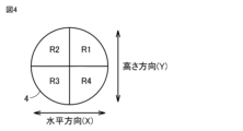
- FIG. 4 is a diagram showing the structure of the light position detector 4. As shown in FIG.
- the optical position detector 4 has four regions R1 to R4, which are formed by dividing a circular or square light receiving element.
- the optical outputs of the regions R1, R2, R3, and R4 are designated as A1, A2, A3, and A4.
- the optical position detector 4 outputs a horizontal (X-direction) position signal HO shown in equation (1) and a height (Y-direction) position signal VO shown in equation (2) to the differential detector 10.
- the differential detector 10 outputs a differential signal DF between the height direction position signal VO and the horizontal direction position signal HO to a calculator 11 .
- the calculator 11 measures the amount or concentration of the component to be measured in the sample 5 based on the difference between a differential signal DF(1) based on the reference position RP at which the emitted probe light 7a is incident, detected by the optical position detector 4, in a reference state in which the excitation light source 1 is not emitting excitation light, and a differential signal DF(2) based on the change position CP at which the emitted probe light 7b is incident, detected by the optical position detector 4, in a change state in which the excitation light source 1 is emitting excitation light.
- an optical position detector 4 capable of outputting the horizontal and vertical positions of the emitted probe light 7a, 7b, and a differential detector 10 that outputs a differential signal of the output of the optical position detector 4, it is possible to remove noise components caused by vibrations that occur commonly in both the horizontal and vertical directions. Furthermore, by detecting all two-dimensional components of the signal generated by changes in the direction of travel of the probe light, it is possible to reduce the effects of vibrations of the optical position detector 4 and increase the signal components, thereby realizing a highly accurate non-invasive component analysis device.
- Embodiment 2. 5 is a diagram showing the configuration of a noninvasive component analysis device according to embodiment 2.
- the noninvasive component analysis device according to embodiment 2 differs from the noninvasive component analysis device according to embodiment 1 in that the noninvasive component analysis device according to embodiment 2 includes an optical chopper 20 between the excitation light source 1 and the optical medium 3, and includes a lock-in amplifier 21 between the differential detector 10 and the calculator 11.
- the optical chopper 20 is disposed in the optical path of the excitation light 6.
- the optical chopper 20 chops the excitation light 6 (continuous light) emitted from the excitation light source 1 at an arbitrary frequency.
- the excitation light 6 becomes intermittent light (pulsed light) that is turned on and off at a period corresponding to the chopping frequency (frequency at which light is turned on and off) of the optical chopper 20, and is incident on the optical medium 3.
- a well-known configuration can be applied to the optical chopper 20.
- the optical chopper 20 has, for example, a rotating disk on which openings that allow the excitation light 6 to pass and light-shielding parts that block the excitation light 6 are arranged in the circumferential direction, and a motor that rotates the rotating disk.
- the excitation light 6 is intensity-modulated at the chopping frequency of the optical chopper 20.
- the chopping frequency of the excitation light 6 is determined by the rotation speed of the rotating disk.
- the optical chopper 20 and the lock-in amplifier 21 are connected to an oscillator (not shown).
- the oscillator sets the chopping frequency (modulation frequency) of the optical chopper 20.
- the oscillator generates a control signal for chopping control of the excitation light 6, and provides the generated control signal to the optical chopper 20 and the lock-in amplifier 21.
- the control signal includes the chopping frequency of the optical chopper 20.
- the lock-in amplifier 21 selectively amplifies the signal that is synchronized with the chopping frequency (modulation frequency) of the optical chopper 20, among the signals related to the position of the probe light 7 output from the optical position detector 4.
- the on-period of the chopping cycle corresponds to the period during which the excitation light 6 is irradiated.
- the off-period of the chopping cycle corresponds to the period during which the excitation light 6 is not irradiated.
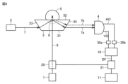
- Embodiment 3. 6 is a diagram showing the configuration of a noninvasive component analysis device according to embodiment 3.
- the noninvasive component analysis device according to embodiment 3 differs from the noninvasive component analysis device according to embodiment 2 in that the noninvasive component analysis device according to embodiment 3 includes filters 30a and 30b between the optical position detector 4 and the differential detector 10.
- Filter 30a selectively transmits a specific frequency band of the height position signal VO of the optical position detector 4.
- Filter 30b selectively transmits a specific frequency band of the horizontal position signal HO of the optical position detector 4.
- Filters 30a and 30b can filter out, for example, frequency bands that contain many vibration components outside the frequency band corresponding to the ON-OFF frequency of the excitation light 6 emitted from the excitation light source 1.
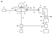
- Embodiment 4. 7 is a diagram showing the configuration of a noninvasive component analysis device according to embodiment 4.
- the noninvasive component analysis device according to embodiment 4 differs from the noninvasive component analysis device according to embodiment 2 in that the noninvasive component analysis device according to embodiment 4 includes gain adjusters 40a and 40b between the optical position detector 4 and the differential detector 10.
- Gain adjuster 40a adjusts the output gain of the height-direction position signal VO of the optical position detector 4.
- Gain adjuster 40b adjusts the output gain of the horizontal-direction position signal HO of the optical position detector 4. For example, when the amplitude of the noise component of the height-direction position signal VO of the optical position detector 4 differs from the amplitude of the noise component of the horizontal-direction position signal HO, gain adjuster 40a and gain adjuster 40b can adjust the amplitude so that the noise component can be removed when differential detection is performed.
- Embodiment 5. 8 is a diagram showing the configuration of a noninvasive component analysis device according to embodiment 5.
- the noninvasive component analysis device according to embodiment 5 differs from the noninvasive component analysis device according to embodiment 2 in that the noninvasive component analysis device according to embodiment 5 includes a light position detector 4A instead of the light position detector 4, and further includes a laser control unit 50.
- the optical position detector 4A detects the intensity of the received emitted probe light 7a, 7b. Specifically, the optical position detector 4A outputs the sum AO of the optical outputs A1, A2, A3, and A4 of the regions R1, R2, R3, and R4.
- the laser control unit 50 controls the output of the probe light source 2 based on the value of the sum AO. This makes it possible to always keep the intensity of the output incident on the light position detector 4A constant, for example. This enables the non-invasive component analysis device to have even higher accuracy.
- Excitation light source 1 Excitation light source, 2 Probe light source, 3 Optical medium, 4, 4A Optical position detector, 5 Sample, 6 Excitation light, 7, 7a, 7b Probe light, 8 Refractive index gradient region, 10 Differential detector, 11 Calculator, 20 Optical chopper, 21 Lock-in amplifier, 30a, 30b Filter, 40a, 40b Gain adjuster, 50 Laser control unit.
Landscapes
- Physics & Mathematics (AREA)
- General Health & Medical Sciences (AREA)
- Life Sciences & Earth Sciences (AREA)
- Chemical & Material Sciences (AREA)
- Analytical Chemistry (AREA)
- Biochemistry (AREA)
- Health & Medical Sciences (AREA)
- General Physics & Mathematics (AREA)
- Immunology (AREA)
- Pathology (AREA)
- Spectroscopy & Molecular Physics (AREA)
- Optics & Photonics (AREA)
- Investigating Or Analysing Materials By Optical Means (AREA)
- Measurement Of The Respiration, Hearing Ability, Form, And Blood Characteristics Of Living Organisms (AREA)
Priority Applications (4)
| Application Number | Priority Date | Filing Date | Title |
|---|---|---|---|
| DE112023006432.6T DE112023006432T5 (de) | 2023-05-31 | 2023-05-31 | Vorrichtung für nichtinvasive bestandteilsanalyse |
| JP2023551201A JP7422956B1 (ja) | 2023-05-31 | 2023-05-31 | 非侵襲成分分析装置 |
| PCT/JP2023/020321 WO2024247177A1 (ja) | 2023-05-31 | 2023-05-31 | 非侵襲成分分析装置 |
| CN202380098395.0A CN121195157A (zh) | 2023-05-31 | 2023-05-31 | 非侵入成分分析装置 |
Applications Claiming Priority (1)
| Application Number | Priority Date | Filing Date | Title |
|---|---|---|---|
| PCT/JP2023/020321 WO2024247177A1 (ja) | 2023-05-31 | 2023-05-31 | 非侵襲成分分析装置 |
Publications (1)
| Publication Number | Publication Date |
|---|---|
| WO2024247177A1 true WO2024247177A1 (ja) | 2024-12-05 |
Family
ID=89620874
Family Applications (1)
| Application Number | Title | Priority Date | Filing Date |
|---|---|---|---|
| PCT/JP2023/020321 Ceased WO2024247177A1 (ja) | 2023-05-31 | 2023-05-31 | 非侵襲成分分析装置 |
Country Status (4)
| Country | Link |
|---|---|
| JP (1) | JP7422956B1 (https=) |
| CN (1) | CN121195157A (https=) |
| DE (1) | DE112023006432T5 (https=) |
| WO (1) | WO2024247177A1 (https=) |
Citations (4)
| Publication number | Priority date | Publication date | Assignee | Title |
|---|---|---|---|---|
| US5268746A (en) * | 1989-09-26 | 1993-12-07 | Ente Per Le Nuove Tecnologie, L'energia E L'ambiente (Enea) | Devices for measuring the optical absorption in thin layer materials by using the photothermal deflection spectroscopy |
| JP6956930B1 (ja) * | 2021-03-23 | 2021-11-02 | 三菱電機株式会社 | 生体成分測定装置および生体成分測定方法 |
| JP6966028B1 (ja) * | 2021-03-03 | 2021-11-10 | 三菱電機株式会社 | 成分測定装置および成分測定方法 |
| JP7205002B1 (ja) * | 2022-02-17 | 2023-01-16 | 三菱電機株式会社 | 非侵襲物質分析装置 |
Family Cites Families (1)
| Publication number | Priority date | Publication date | Assignee | Title |
|---|---|---|---|---|
| DE102014108424B3 (de) | 2014-06-16 | 2015-06-11 | Johann Wolfgang Goethe-Universität | Nicht-invasive Stoffanalyse |
-
2023
- 2023-05-31 JP JP2023551201A patent/JP7422956B1/ja active Active
- 2023-05-31 CN CN202380098395.0A patent/CN121195157A/zh active Pending
- 2023-05-31 DE DE112023006432.6T patent/DE112023006432T5/de active Pending
- 2023-05-31 WO PCT/JP2023/020321 patent/WO2024247177A1/ja not_active Ceased
Patent Citations (4)
| Publication number | Priority date | Publication date | Assignee | Title |
|---|---|---|---|---|
| US5268746A (en) * | 1989-09-26 | 1993-12-07 | Ente Per Le Nuove Tecnologie, L'energia E L'ambiente (Enea) | Devices for measuring the optical absorption in thin layer materials by using the photothermal deflection spectroscopy |
| JP6966028B1 (ja) * | 2021-03-03 | 2021-11-10 | 三菱電機株式会社 | 成分測定装置および成分測定方法 |
| JP6956930B1 (ja) * | 2021-03-23 | 2021-11-02 | 三菱電機株式会社 | 生体成分測定装置および生体成分測定方法 |
| JP7205002B1 (ja) * | 2022-02-17 | 2023-01-16 | 三菱電機株式会社 | 非侵襲物質分析装置 |
Also Published As
| Publication number | Publication date |
|---|---|
| CN121195157A (zh) | 2025-12-23 |
| JPWO2024247177A1 (https=) | 2024-12-05 |
| JP7422956B1 (ja) | 2024-01-26 |
| DE112023006432T5 (de) | 2026-03-26 |
Similar Documents
| Publication | Publication Date | Title |
|---|---|---|
| CN106535760B (zh) | 非侵入性物质分析 | |
| JP7423622B2 (ja) | 物質を分析するための装置および方法 | |
| AU711422B2 (en) | Process and device for determining an analyte contained in a scattering matrix | |
| Pleitez et al. | Photothermal deflectometry enhanced by total internal reflection enables non-invasive glucose monitoring in human epidermis | |
| JPS60236631A (ja) | グルコースの測光検出装置 | |
| JPWO2013129519A1 (ja) | 分光特性測定装置及び分光特性測定方法 | |
| US20080269580A1 (en) | System for Non-Invasive Measurement of Bloold Glucose Concentration | |
| CN113349768A (zh) | 测定装置以及生物体信息测定装置 | |
| KR101103091B1 (ko) | 파장 라우터를 이용한 전자기 스펙트럼으로부터의 시료의측정 | |
| WO2012134515A1 (en) | Method and apparatus for in vivo optical measurement of blood glucose concentration | |
| JPH1189799A (ja) | 特定成分の濃度測定装置および濃度測定方法 | |
| JP2010515046A (ja) | 分光測定 | |
| WO2024247177A1 (ja) | 非侵襲成分分析装置 | |
| JPWO2006051778A1 (ja) | 生体情報測定用光学素子およびそれを用いた生体情報測定装置 | |
| JP2004313554A (ja) | 血糖値の非侵襲測定装置 | |
| JP6871197B2 (ja) | 成分濃度測定装置 | |
| JP7205002B1 (ja) | 非侵襲物質分析装置 | |
| JP7466817B1 (ja) | 分析装置 | |
| JP7638461B1 (ja) | 非侵襲物質分析装置及び非侵襲物質分析方法 | |
| JP6080004B2 (ja) | パラメータ計測装置、パラメータ計測方法、及びプログラム | |
| JP7736944B1 (ja) | 生体成分測定装置 | |
| EP4158312B1 (en) | Apparatus and method for analyte measurement with improved coupling of excitation radiation into material including said analyte | |
| RU2813964C2 (ru) | Устройство и способ анализа вещества | |
| JP2003240709A (ja) | 特定成分の濃度測定方法及びそれに用いる濃度測定用接触子 | |
| JPH09182740A (ja) | 生体の光学的測定装置 |
Legal Events
| Date | Code | Title | Description |
|---|---|---|---|
| WWE | Wipo information: entry into national phase |
Ref document number: 2023551201 Country of ref document: JP |
|
| 121 | Ep: the epo has been informed by wipo that ep was designated in this application |
Ref document number: 23939652 Country of ref document: EP Kind code of ref document: A1 |
|
| WWE | Wipo information: entry into national phase |
Ref document number: 112023006432 Country of ref document: DE |
|
| WWP | Wipo information: published in national office |
Ref document number: 112023006432 Country of ref document: DE |