WO2024241936A1 - 基板処理方法及び基板処理装置 - Google Patents
基板処理方法及び基板処理装置 Download PDFInfo
- Publication number
- WO2024241936A1 WO2024241936A1 PCT/JP2024/017598 JP2024017598W WO2024241936A1 WO 2024241936 A1 WO2024241936 A1 WO 2024241936A1 JP 2024017598 W JP2024017598 W JP 2024017598W WO 2024241936 A1 WO2024241936 A1 WO 2024241936A1
- Authority
- WO
- WIPO (PCT)
- Prior art keywords
- laser
- substrate
- laser light
- wafer
- irradiation
- Prior art date
- Legal status (The legal status is an assumption and is not a legal conclusion. Google has not performed a legal analysis and makes no representation as to the accuracy of the status listed.)
- Ceased
Links
Images







Classifications
-
- B—PERFORMING OPERATIONS; TRANSPORTING
- B23—MACHINE TOOLS; METAL-WORKING NOT OTHERWISE PROVIDED FOR
- B23K—SOLDERING OR UNSOLDERING; WELDING; CLADDING OR PLATING BY SOLDERING OR WELDING; CUTTING BY APPLYING HEAT LOCALLY, e.g. FLAME CUTTING; WORKING BY LASER BEAM
- B23K26/00—Working by laser beam, e.g. welding, cutting or boring
-
- B—PERFORMING OPERATIONS; TRANSPORTING
- B23—MACHINE TOOLS; METAL-WORKING NOT OTHERWISE PROVIDED FOR
- B23K—SOLDERING OR UNSOLDERING; WELDING; CLADDING OR PLATING BY SOLDERING OR WELDING; CUTTING BY APPLYING HEAT LOCALLY, e.g. FLAME CUTTING; WORKING BY LASER BEAM
- B23K26/00—Working by laser beam, e.g. welding, cutting or boring
- B23K26/02—Positioning or observing the workpiece, e.g. with respect to the point of impact; Aligning, aiming or focusing the laser beam
- B23K26/06—Shaping the laser beam, e.g. by masks or multi-focusing
- B23K26/062—Shaping the laser beam, e.g. by masks or multi-focusing by direct control of the laser beam
- B23K26/0622—Shaping the laser beam, e.g. by masks or multi-focusing by direct control of the laser beam by shaping pulses
-
- B—PERFORMING OPERATIONS; TRANSPORTING
- B23—MACHINE TOOLS; METAL-WORKING NOT OTHERWISE PROVIDED FOR
- B23K—SOLDERING OR UNSOLDERING; WELDING; CLADDING OR PLATING BY SOLDERING OR WELDING; CUTTING BY APPLYING HEAT LOCALLY, e.g. FLAME CUTTING; WORKING BY LASER BEAM
- B23K26/00—Working by laser beam, e.g. welding, cutting or boring
- B23K26/02—Positioning or observing the workpiece, e.g. with respect to the point of impact; Aligning, aiming or focusing the laser beam
- B23K26/06—Shaping the laser beam, e.g. by masks or multi-focusing
- B23K26/064—Shaping the laser beam, e.g. by masks or multi-focusing by means of optical elements, e.g. lenses, mirrors or prisms
-
- B—PERFORMING OPERATIONS; TRANSPORTING
- B23—MACHINE TOOLS; METAL-WORKING NOT OTHERWISE PROVIDED FOR
- B23K—SOLDERING OR UNSOLDERING; WELDING; CLADDING OR PLATING BY SOLDERING OR WELDING; CUTTING BY APPLYING HEAT LOCALLY, e.g. FLAME CUTTING; WORKING BY LASER BEAM
- B23K26/00—Working by laser beam, e.g. welding, cutting or boring
- B23K26/02—Positioning or observing the workpiece, e.g. with respect to the point of impact; Aligning, aiming or focusing the laser beam
- B23K26/06—Shaping the laser beam, e.g. by masks or multi-focusing
- B23K26/067—Dividing the beam into multiple beams, e.g. multi-focusing
-
- B—PERFORMING OPERATIONS; TRANSPORTING
- B23—MACHINE TOOLS; METAL-WORKING NOT OTHERWISE PROVIDED FOR
- B23K—SOLDERING OR UNSOLDERING; WELDING; CLADDING OR PLATING BY SOLDERING OR WELDING; CUTTING BY APPLYING HEAT LOCALLY, e.g. FLAME CUTTING; WORKING BY LASER BEAM
- B23K26/00—Working by laser beam, e.g. welding, cutting or boring
- B23K26/08—Devices involving relative movement between laser beam and workpiece
Definitions
- This disclosure relates to a substrate processing method and a substrate processing apparatus.
- Patent Document 1 discloses a substrate processing method in which a laser absorption layer of a laminated substrate is irradiated with pulsed laser light. Patent Document 1 discloses that by providing a laser irradiation device with multiple laser irradiation units and irradiating the laser absorption layer with multiple laser beams, processing time can be shortened and throughput improved.
- the technology disclosed herein efficiently irradiates a substrate with laser light for processing.
- One aspect of the present disclosure is a substrate processing method for processing a substrate, which includes irradiating the substrate with pulsed laser light, and when irradiating the laser light, a branching element is inserted or removed from the optical path of the laser light irradiated from a laser head according to a preset area of the substrate.
- the irradiation of the laser light can be performed efficiently.
- FIG. 1 is a side view showing an outline of a configuration of overlapping wafers processed in a wafer processing system.
- 1 is a plan view illustrating a schematic configuration of a wafer processing system.
- FIG. 2 is a side view showing an outline of the configuration of a laser irradiation device.
- FIG. 2 is a plan view showing an outline of the configuration of a laser irradiation device.
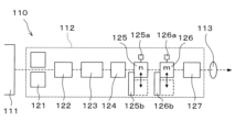
- FIG. 2 is an explanatory diagram illustrating a schematic outline of the configuration of an optical system of a laser irradiation device.
- FIG. 10 is an explanatory diagram showing how laser light is split by one splitting element.
- FIG. 2 is an explanatory diagram showing how laser light is branched by a plurality of branching elements.
- FIG. 4 is an explanatory diagram showing a state in which a laser absorption layer is irradiated with laser light.
- FIG. 13 is an explanatory diagram showing a state in which the first wafer is separated from the laser absorption layer.
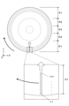
- FIG. 4 is an explanatory diagram showing the intervals between irradiation points of laser light.
- 11 is an explanatory diagram showing a state in which a laser beam is irradiated onto an outer circumferential region.
- FIG. 13A and 13B are explanatory diagrams showing another example of irradiation of the outer circumferential region with laser light.
- FIG. 13 is an explanatory diagram showing how a central region is irradiated with laser light.
- FIG. 13 is an explanatory diagram showing how a central region is irradiated with laser light.
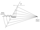
- FIG. 4 is an explanatory diagram showing radial intervals of laser light. 4 is an explanatory diagram showing the relationship between the radial position of the laser absorbing layer and the radial interval of laser light.
- FIG. 4 is an explanatory diagram showing a state in which a laser absorbing layer is irradiated with laser light.
- a device layer formed on the surface of a first substrate is transferred to a second substrate.
- This transfer of the device layer is performed using a method known as laser lift-off, in which a laser absorption layer formed between the first substrate and the device layer is irradiated with laser light in a laminated substrate in which the first substrate and the second substrate are bonded together, thereby peeling off the interface between the first substrate and the laser absorption layer.
- the laminated substrate is rotated and the laser light is irradiated in pulses while the irradiation position of the laser light is moved from the outside to the inside in the radial direction of the laminated substrate.
- the interval between the laser light irradiation positions on the laser absorbing layer is kept constant.
- the circumferential speed of the laminated substrate accompanying the rotation differs depending on the radial position of the irradiation position, so it is necessary to increase the rotation speed of the laminated substrate as the irradiation position moves from the outer side to the inner side in the radial direction.
- the rotation speed of the laminated substrate reaches the upper limit, as the laser light irradiation position moves radially inward, the interval between the circumferential positions of the laser light irradiation positions becomes smaller, and the laser light may overlap in the center. In such a case, more energy than necessary is supplied to the laser absorbing layer, and the device layer may be damaged by the generated heat. In addition, the laser absorbing layer may not be able to absorb all the laser light, which may reach the device layer and cause damage by the laser light.
- the technology according to the present disclosure has been made in consideration of the above circumstances, and when a substrate is irradiated with laser light for processing, the laser light is irradiated efficiently.
- the substrate and the laser absorbing layer are peeled off by irradiation with laser light in this manner, and the "peeling" of the substrate and the laser absorbing layer includes a state in which the substrate is completely peeled off from the laser absorbing layer and the adhesion force therebetween becomes zero, and a state in which the adhesion force between the substrate and the laser absorbing layer still remains but the adhesion strength has decreased to such an extent that the substrate and the laser absorbing layer can be easily separated by a transfer pad or a separation device described later.
- separation refers to bringing the substrate and the laser absorption layer into a state where they are not in contact with each other (a state where the substrate is lifted up from the laser absorption layer), for example, by using a carrier pad or the like described below.
- a laminated wafer T which is a substrate formed by bonding a first wafer W and a second wafer S together, as shown in FIG. 1.
- a wafer is an example of a substrate.
- the surface of the first wafer W that is bonded to the second wafer S is referred to as the front surface Wa
- the surface opposite the front surface Wa is referred to as the back surface Wb.
- the surface of the second wafer S that is bonded to the first wafer W is referred to as the front surface Sa
- the surface opposite the front surface Sa is referred to as the back surface Sb.
- the first wafer W is a semiconductor wafer such as a silicon substrate, and at least one film is laminated on the front surface Wa.
- the film formed on the front surface Wa is referred to as a "laminated film".
- the laminated film includes a laser absorbing layer Ap, a device layer Dw, and a bonding film Fw.
- the laser absorbing layer Ap is, for example, an oxide film (SiO 2 film), but is not particularly limited as long as it absorbs the laser light L irradiated from the laser irradiation unit 110 described later.
- the device layer Dw includes a plurality of devices.
- the bonding film Fw is, for example, an oxide film (THOX film, SiO 2 film, TEOS film), a SiC film, a SiCN film, or an adhesive.
- the laser light L irradiated from the laser irradiation unit 110 is absorbed by the laser absorbing layer Ap, which causes peeling at the interface between the first wafer W and the laser absorbing layer Ap, and the device layer Dw is transferred to the second wafer S side.
- the second wafer S is a semiconductor wafer such as a silicon substrate, and has a laminated film formed on the surface Sa side.
- the laminated film includes a device layer Ds and a bonding film Fs.
- the device layer Ds and the bonding film Fs are similar to the device layer Dw and the bonding film Fw of the first wafer W, respectively.
- the laminated wafer T is formed by bonding the bonding film Fw of the first wafer W and the bonding film Fs of the second wafer S.
- the types, number of layers, and order of layers in the laminated film formed on the front surface Wa of the first wafer W and the front surface Sa of the second wafer S are not limited to those shown in the figures.
- a laser absorbing layer Ap may be formed between the device layer Dw and the bonding film Fw.
- the device layer Dw and the bonding film Fw may not be formed on the front surface Wa of the first wafer W.
- the laser absorbing layer Ap is formed on the second wafer S side, and the device layer Ds on the second wafer S side is transferred to the first wafer W side.
- the device layer Ds and the bonding film Fs may not be formed on the front surface Sa of the second wafer S.
- a peeling promoting film (not shown) for promoting peeling between the first wafer W and the second wafer S may be formed between the first wafer W and the laser absorbing layer Ap on the front surface Wa side of the first wafer W, and peeling may occur at the interface between the peeling promoting film and the first wafer W.
- it is desirable to select a peeling promoting film such that the adhesion between the peeling promoting film and the first wafer W (silicon or the like) is at least smaller than the adhesion between the peeling promoting film and the laser absorbing layer Ap (oxide film).
- the wafer processing system 1 has a configuration in which a load/unload block 10, a transport block 20, and a processing block 30 are connected together.
- the load/unload block 10 and the processing block 30 are provided around the transport block 20.
- the load/unload block 10 is disposed on the negative Y-axis side of the transport block 20.
- a laser irradiation device 31 (described later) of the processing block 30 is disposed on the negative X-axis side of the transport block 20, and a cleaning device 32 (described later) is disposed on the positive X-axis side of the transport block 20.
- the loading/unloading block 10 loads/unloads cassettes Ct, Cw, and Cs, each capable of accommodating multiple overlapped wafers T, multiple first wafers W, and multiple second wafers S, for example, between the outside and the device.
- the loading/unloading block 10 is provided with a cassette mounting table 11.
- the cassette mounting table 11 can freely mount multiple cassettes Ct, Cw, and Cs, for example, three cassettes Ct, Cw, and Cs, in a line in the X-axis direction.
- the number of cassettes Ct, Cw, and Cs mounted on the cassette mounting table 11 is not limited to this embodiment and can be determined arbitrarily.
- the transport block 20 is provided with a wafer transport device 22 that is movable on a transport path 21 extending in the X-axis direction.
- the wafer transport device 22 has, for example, two transport arms 23, 23 that hold and transport the overlapped wafer T, the first wafer W, and the second wafer S.
- Each transport arm 23 is configured to be movable horizontally, vertically, around a horizontal axis, and around a vertical axis. Note that the configuration of the transport arm 23 is not limited to this embodiment, and any configuration may be used.
- the wafer transport device 22 is configured to be able to transport the overlapped wafer T, the first wafer W, and the second wafer S to the cassettes Ct, Cw, and Cs on the cassette mounting table 11, the laser irradiation device 31, and the cleaning device 32, which will be described later.
- the processing block 30 has a laser irradiation device 31 and a cleaning device 32.
- the laser irradiation device 31 irradiates the laser absorption layer Ap of the first wafer W with laser light (e.g., CO2 laser) to cause peeling at the interface between the first wafer W and the laser absorption layer Ap, thereby transferring the device layer Dw formed on the front surface Wa of the first wafer W to the second wafer S.
- the laser irradiation device 31 also has a control device 31a described later.
- the laser irradiation device 31 has a chuck 100 as a substrate holding part that holds the overlapped wafer T on its upper surface.
- the chuck 100 adsorbs and holds the entire back surface Sb of the second wafer S.
- the chuck 100 may also adsorb and hold a portion of the back surface Sb.
- the chuck 100 is provided with lifting pins (not shown) for supporting and raising and lowering the overlapped wafer T from below.
- the lifting pins are inserted through through holes (not shown) formed through the chuck 100, and are configured to be freely raised and lowered.
- the chuck 100 is supported by the slider table 102 via an air bearing 101.
- a holder rotation mechanism 103 is provided on the underside of the slider table 102.
- the holder rotation mechanism 103 has a built-in motor as a drive source.
- the chuck 100 is configured to be rotatable around the ⁇ -axis (vertical axis) via the air bearing 101 by the holder rotation mechanism 103.
- the slider table 102 is configured to be movable along a rail 105 that is provided on a base 106 and extends in the Y-axis direction by a holder movement mechanism 104 provided on the underside of the slider table 102.
- the drive source of the holder movement mechanism 104 is not particularly limited, but a linear motor is used, for example.
- a laser irradiation unit 110 is provided above the chuck 100.
- the laser irradiation unit 110 has a laser head 111, an optical system 112, and a lens 113.
- the lens 113 may be configured to be freely raised and lowered by a lifting mechanism (not shown).
- the laser head 111 has a laser oscillator (not shown) that oscillates a laser beam in a pulsed manner.
- This laser beam is a so-called pulsed laser.
- the laser beam is a CO2 laser beam, and the wavelength of the CO2 laser beam is, for example, 8.9 ⁇ m to 11 ⁇ m.
- the laser head 111 may have other devices besides the laser oscillator, such as an amplifier.
- the optical system 112 includes an iris 121, an expander 122, an isolator 123, an attenuator 124, a first branching element 125, a second branching element 126, and a galvanometer mirror 127.
- the iris 121 cuts the laser light emitted from the laser head 111 and shapes it into a desired shape.
- the expander 122 adjusts the diameter of the laser light emitted from the laser head 111 .
- the isolator 123 prevents reflected light (return light) from the overlapped wafer T, which is the target of irradiation with the laser light, from returning and entering the laser head 111 .
- the attenuator 124 attenuates the laser light emitted from the laser head 111 to adjust the output.
- the galvanometer mirror 127 is configured to be capable of adjusting the angle of incidence of the laser light irradiated from the laser head 111 side with respect to the galvanometer mirror 127, and is configured to be capable of scanning the laser light with respect to the laminated wafer T.
- Scanning the laser light L means moving the laser light L irradiated from the lens 113 of the laser irradiation unit 110 with respect to the laser absorption layer Ap.
- the first and second branching elements 125 and 126 branch one laser beam L incident from the laser head 111 side into a plurality of laser beams L whose irradiation points are arranged in a line distribution (on a straight line).
- the configuration of the branching elements is arbitrary, and for example, DOEs (Diffractive Optical Elements) or prisms are used.
- the number of branches of the laser beam L by the first and second branching elements 125 and 126 is not particularly limited, but in this embodiment, the number of branches of the first branching element 125 and the second branching element 126 are different from each other. In the following description, as shown in FIG. 5 and FIG.
- each of the branched laser beams may be expressed as "branched laser beams L 1 to L n (branched laser beams L 1 to L m )" according to the number of branches.
- the first and second splitting elements 125, 126 are each equipped with a rotation mechanism 125a, 126a, and are configured to be rotatable about an axis relative to the optical path of the laser light. This allows the arrangement of the irradiation points of the multiple laser beams arranged in a line distribution, in other words, the direction in which the multiple irradiation points on the laser absorption layer Ap irradiated with the laser light are arranged, to be controlled.
- the type and configuration of the rotation mechanisms 125a, 126a are not particularly limited, but for example, a piezoelectric motor can be used.
- the first and second branching elements 125, 126 are each provided with a moving mechanism 125b, 126b, and as shown in FIG. 5, are configured to be freely inserted and removed from the optical path of the laser light in the optical system 112.
- the moving mechanisms 125b, 126b there are no particular limitations on the type or configuration of the moving mechanisms 125b, 126b, and any linear or rotary moving mechanism can be selected, for example, an actuator or slider mechanism can be used.
- the number of branches of the laser light L output from the laser head 111 and irradiated to the overlapped wafer T can be arbitrarily controlled by controlling the insertion and removal of the first branching element 125 and the second branching element 126 from the optical path.
- a single laser beam irradiated from the laser head 111 can be branched into n ⁇ m branched laser beams arranged in an approximately rectangular shape.
- a single laser beam irradiated from the laser head 111 can be branched into n branch laser beams arranged in a line distribution.
- one laser beam irradiated from the laser head 111 can be branched into m branched laser beams arranged in a line distribution. Furthermore, by removing both the first branching element 125 and the second branching element 126 from the optical path, the single laser light irradiated from the laser head 111 can be irradiated onto the overlapped wafer T as a single laser light without being branched.
- moving mechanisms 125b and 126b are arranged independently for the first and second branching elements 125 and 126, respectively.
- the optical system 112 may have only one moving mechanism common to each of the first and second branching elements 125 and 126.
- the lens 113 irradiates the laser light onto the laminated wafer T held by the chuck 100.
- the laser light emitted from the laser irradiation unit 110 passes through the first wafer W and is irradiated onto the laser absorption layer Ap.
- a transfer pad 130 is further provided above the chuck 100.
- the transfer pad 130 is configured to be freely raised and lowered by a lifting mechanism (not shown).
- the transfer pad 130 has an adsorption surface for the first wafer W.
- the transfer pad 130 transfers the first wafer W between the chuck 100 and the transfer arm 23. Specifically, after the chuck 100 is moved to a position below the transfer pad 130 (a transfer position with the transfer arm 23), the transfer pad 130 adsorbs and holds the back surface Wb of the first wafer W and separates it from the second wafer S. Next, the separated first wafer W is transferred from the transfer pad 130 to the transfer arm 23 and carried out of the laser irradiation device 31.
- the cleaning device 32 cleans the second wafer S and/or the first wafer W after separation in the laser irradiation device 31 .
- the above-described wafer processing system 1 is provided with a control device 31a and at least one control device 40 as a control unit.
- the control device 31a individually controls the operation of the laser irradiation device 31.
- the control device 40 manages the control of a series of wafer processes in the wafer processing system 1.
- the control devices 31a and 40 each process computer-executable instructions that cause the laser irradiation device 31 and the wafer processing system 1 to execute various processes described in this disclosure.
- the control devices 31a and 40 can each be configured to control each element of the laser irradiation device 31 and the wafer processing system 1 to execute various processes described herein.
- a part or all of the control device 31a may be included in the laser irradiation device 31, and a part or all of the control device 40 may be included in the wafer processing system 1.
- the control device 31a and the control device 40 may each include a processing unit, a storage unit, and a communication interface.
- the control device 31a and the control device 40 are each realized by, for example, a computer.
- the processing unit may be configured to read a program that provides a logic or routine that enables various control operations to be performed from the storage unit, and to perform various control operations by executing the read program.
- This program may be stored in the storage unit in advance, or may be acquired via a medium when necessary. The acquired program is stored in the storage unit, and is read from the storage unit by the processing unit and executed.
- the medium may be various storage media H that can be read by a computer, or may be a communication line connected to the communication interface.
- the storage unit has a program storage unit (not shown).
- the program storage unit stores a program for controlling the processing of the laminated wafer T in the wafer processing system 1.
- the program storage unit also stores a program for controlling the operation of the drive system such as the various processing devices and the transport device described above to realize the wafer processing in the wafer processing system 1 described later.
- the above program may be recorded in a storage medium H that can be read by a computer, and may be installed in the control device 31a and the control device 40 from the storage medium H.
- the storage medium H may be temporary or non-temporary.
- the processing unit may be a CPU (Central Processing Unit) or one or more circuits.
- the storage unit may include a RAM (Random Access Memory), a ROM (Read Only Memory), a HDD (Hard Disk Drive), an SSD (Solid State Drive), or a combination thereof.
- the communication interface may communicate between the laser irradiation device 31 and the wafer processing system 1 via a communication line such as a LAN (Local Area Network).
- the control device 31a and the control device 40 are installed separately for the laser irradiation device 31 and the wafer processing system 1, respectively, but the control device 31a and the control device 40 may be configured as an integrated device. In other words, the operation of the laser irradiation device 31 may be controlled by the control device 40.
- the first wafer W and the second wafer S are bonded in a bonding device (not shown) external to the wafer processing system 1 to form a laminated wafer T in advance.
- a cassette Ct containing multiple overlapping wafers T is placed on the cassette placement table 11 of the load/unload block 10.
- the overlapping wafers T in the cassette Ct are removed by the wafer transfer device 22 and transferred to the laser irradiation device 31.
- the overlapping wafers T held by the transfer arm 23 of the wafer transfer device 22 are transferred to the chuck 100 of the laser irradiation device 31.
- a laser irradiation unit 110 irradiates a laser light L ( CO2 laser light) in a pulsed manner toward the laser absorbing layer Ap of the overlapped wafer T.
- the laser light L passes through the first wafer W from the rear surface Wb side of the first wafer W and is absorbed in the laser absorbing layer Ap.
- the overlapped wafer T is rotated and the laser light L is moved from the outer side to the inner side in the radial direction, so that the laser light L is irradiated onto the entire surface of the laser absorbing layer Ap. Note that a specific irradiation method of the laser light L will be described later.
- the laser light L absorbed in the laser absorption layer Ap is converted into heat at the irradiation point of the laser light L according to its energy distribution.
- the temperature of the laser absorption layer Ap rises due to irradiation with the laser light L
- the temperature of the interface between the first wafer W and the laser absorption layer Ap rises further due to the diffusion of heat.
- the first wafer W locally expands (plastically deforms downwardly convexly relative to the laser absorption layer Ap side) according to the temperature distribution.
- the laser absorption layer Ap is pressed from the upper side (first wafer W side) with the expansion of the first wafer W, and the stress acting due to this pressing causes peeling at the interface between the laser absorption layer Ap and the first wafer W. Therefore, in the laser irradiation device 31, as described above, the laser light L is irradiated in a pulsed manner onto the entire surface of the laser absorption layer Ap, and the thermal effect caused by the irradiation of the laser light L causes peeling over the entire surface of the interface between the laser absorption layer Ap and the first wafer W.
- the back surface Wb of the first wafer W is adsorbed and held by the transfer pad 130.
- the transfer pad 130 is raised to separate the first wafer W from the laser absorption layer Ap (second wafer S).
- peeling has occurred at the interface between the laser absorption layer Ap and the first wafer W due to the irradiation of the laser light L, so that the first wafer W can be separated from the laser absorption layer Ap without applying a large load.
- the transfer pad 130 may be rotated around the vertical axis to separate the first wafer W.
- the separated first wafer W is transferred from the transfer pad 130 to the transfer arm 23 of the wafer transfer device 22 and transferred to the cassette Cw on the cassette mounting table 11.
- the first wafer W removed from the laser irradiation device 31 may be transferred to the cleaning device 32 before being transferred to the cassette Cw, and its separated surface Wa may be cleaned.
- the first wafer W may be inverted from the front to the back by the transfer pad 130 and transferred to the transfer arm 23.
- the second wafer S held by the chuck 100 is transferred by the transfer arm 23 to the cleaning device 32 and cleaned. Thereafter, the second wafer S on which all the processes have been performed is transferred by the wafer transfer device 22 to the cassette Cs on the cassette mounting table 11. In this manner, a series of wafer processes in the wafer processing system 1 is completed.
- the first wafer W is completely separated from the laser absorption layer Ap (second wafer S) by the transfer pad 130 provided in the laser irradiation device 31.
- the laser absorption layer Ap (second wafer S) and the first wafer W may be separated in a separation device arranged independently of the laser irradiation device 31.
- the separation device (not shown) may be arranged, for example, on the positive Y-axis side of the transfer block 20 in the wafer processing system 1.
- the laser light L is split into multiple beams using a splitting element as described above and irradiated simultaneously. Also, in order to perform the peeling of the first wafer W and the laser absorbing layer Ap uniformly within the wafer surface, the wafer processing is controlled so that the interval of the laser light L irradiated to the laser absorbing layer Ap, more specifically, the interval between the irradiation points on the laser absorbing layer Ap, is constant within the wafer surface. Specifically, the interval of the laser light L in the radial direction of the laser absorbing layer Ap (see FIG. 10.
- the radial interval P can be controlled, for example, by the amount of movement of the chuck 100 (superimposed wafer T) in the Y-axis direction.
- the interval of the laser light L in the circumferential direction of the laser absorbing layer Ap (see FIG. 10.
- the circumferential interval Q" can be controlled, for example, by the rotation speed of the chuck 100 (superimposed wafer T).
- the circumferential spacing Q gradually decreases as the position of the irradiation point moves radially inward, and particularly in the central portion, as shown in the shaded area of FIG. 10, the thermal effects of multiple laser beams L may overlap and act on the same location. This concern is considered to be more pronounced when the laser beam L is branched by a branching element and irradiated, if the number of branches is large and the distance between the radially innermost irradiation point and the radially outermost irradiation point is large.
- the optical system 112 described above controls the movement of the first and second branching elements 125, 126 into and out of the optical path by the moving mechanisms 125b, 126b, and the axial rotation of the first and second branching elements 125, 126 into the optical path by the rotating mechanisms 125a, 126a, thereby appropriately adjusting the interval between the irradiation points on the laser absorption layer Ap (particularly the circumferential interval Q).
- the "appropriate irradiation point interval" is an interval at which the thermal effects do not overlap at least between adjacent irradiation points, and the first wafer W and the laser absorption layer Ap can be appropriately peeled off.
- the interval between the irradiation points it is desirable to control the interval between the irradiation points to be constant within the wafer surface, but as long as the thermal effects do not overlap at least between adjacent irradiation points, and the first wafer W and the laser absorption layer Ap can be appropriately peeled off, the interval between the irradiation points does not necessarily need to be constant.
- the outer peripheral region R1 is an annular region located at the outermost radial position of the laser absorbing layer Ap, which is the target of irradiation with the laser light L.
- the central region R3 is a circular region located at the innermost radial position of the laser absorbing layer Ap.
- the central region R2 is an annular region located between the outer peripheral region R1 and the central region R3 in the radial direction in the laser absorbing layer Ap.
- the outer peripheral region R1, the central region R2, and the central region R3 are preset prior to processing in the laser irradiation device 31 based on various conditions, such as the pulse interval of the laser light L and the rotation speed of the chuck 100.
- the laser light L irradiated from the lens 113 is moved from the radial outside to the inside of the laser absorption layer Ap, and the laser light L is sequentially irradiated to the outer circumferential region R1, the central region R2, and the central region R3 in this order.
- the laser light L from the laser head 111 is branched into a plurality of branched laser lights L1,1 to Ln ,m in the present embodiment, and the branched laser lights L1,1 to Ln ,m are simultaneously irradiated in a pulsed manner in the laser irradiation unit 110.
- the laser light L from the laser head 111 is branched into a plurality of branched laser lights L1,1 to Ln ,m in the present embodiment, and the branched laser lights L1,1 to Ln ,m are simultaneously irradiated in a pulsed manner in the laser irradiation unit 110.
- the branched laser lights L1,1 to Ln ,m are irradiated onto the laser absorption layer Ap in an irradiation point arrangement of an approximately square shape of n x m in plan view.
- the first and second branching elements 125, 126 are rotated by the rotating mechanisms 125a, 126a so that the long side of the approximately square shape (the arrangement direction of the branched laser lights L1,1 to L1 ,m in the present embodiment) is arranged along the radial direction of the laser absorption layer Ap as shown in Fig. 11.
- the holder rotation mechanism 103 rotates the chuck 100 (superimposed wafer T) 360° in the circumferential direction and the holder movement mechanism 104 moves the chuck 100 in the negative Y-axis direction alternately and repeatedly.
- the branched laser light L1,1 to Ln ,m is irradiated onto the outer peripheral region R1 in a ring shape concentric with the laser absorption layer Ap.
- the branched laser light L is irradiated onto the entire surface of the outer peripheral region R1.
- both of the two branching elements are arranged on the optical path in the outer peripheral region R1 radially outside the laser absorption layer Ap, where the circumferential interval Q of the irradiation points is not affected by the relationship between the rotation speed of the chuck 100 (superimposed wafer T) and the pulse interval of the laser light L (the circumferential interval Q can be appropriately maintained by controlling the rotation speed of the chuck 100).
- the laser light L from the laser head 111 is irradiated onto the laser absorption layer Ap as n ⁇ m branched laser light L 1,1 to L n,m .
- the output of the laser head 111 (light source) is insufficient and the amount of energy for each of the branched laser light L 1,1 to L n,m cannot be secured, or when the rotation speed of the chuck 100 (superimposed wafer T) is insufficient and the movement amount of the short side portion of the approximately rectangular shape of n ⁇ m (in this embodiment, the arrangement direction of the branched laser light L 1,1 to L n,1 ) cannot be secured at the pulse interval of the laser light L, instead of arranging both of the two branching elements on the optical path, only the second branching element 126 with a large number of branches may be arranged on the optical path.
- the laser light L from the laser head 111 may be irradiated onto the laser absorption layer Ap as m branched laser light L 1 to L m arranged in a line distribution.
- the second branching element 126 is rotated around the optical axis by the rotating mechanism 126a so that the multiple irradiation points (extension direction of the line distribution) of the branched laser beams L 1 to L m having a line distribution are arranged along the radial direction of the laser absorption layer Ap.
- one laser beam L is branched into multiple branched laser beams L 1 to L m and simultaneously irradiated onto the laser absorption layer Ap, so that the processing time until the laser beam L is irradiated onto the entire surface of the outer circumferential region R1 can be shortened, the throughput can be improved, and the amount of energy per each of the branched laser beams L 1 to L m can be easily secured.
- the number of branches of the laser light L is changed.
- the first branching element 125 having a small number of branches is arranged on the optical path, so that the laser light L from the laser head 111 is branched into a plurality of branched laser lights L1 to Ln in the laser irradiation unit 110, n of which are branched laser lights L1 to Ln in this embodiment, and these branched laser lights L1 to Ln are irradiated simultaneously in a pulsed manner.
- the branched laser lights L1 to Ln are irradiated onto the laser absorption layer Ap in a line-distributed irradiation point arrangement in a plan view, as shown in Fig. 6.
- the first branching element 125 is rotated around the optical axis by the rotation mechanism 125a so that the irradiation points of the line distribution are arranged along the radial direction of the laser absorption layer Ap, as shown in Fig. 13.
- the holder rotation mechanism 103 rotates the chuck 100 (superimposed wafer T) 360° in the circumferential direction and the holder movement mechanism 104 moves the chuck 100 in the negative Y-axis direction alternately and repeatedly.
- the central region R2 is irradiated with the branched laser light L in a ring shape concentric with the laser absorption layer Ap.
- the entire surface of the central region R2 is irradiated with the branched laser light L1 to Ln .
- the number of branches of the laser light L from the laser head 111 is reduced. More specifically, the number of irradiation points arranged in the radial direction of the laser absorption layer Ap is reduced (from m to n in this embodiment).
- the distance from the outermost irradiation point to the innermost irradiation point is smaller than in the outer peripheral region R1, and the difference in circumferential speed between the outer peripheral irradiation point and the inner peripheral irradiation point is reduced, suppressing the overlap of thermal effects at adjacent irradiation points on the inner peripheral side.
- the central region R2 by branching one laser beam L into a plurality of branched laser beams L1 to Ln in this manner and irradiating the laser absorption layer Ap simultaneously, it is possible to shorten the processing time and improve the throughput, at least as compared with the case where the laser beam L is irradiated without being branched.
- the number of branches of the laser light L is further changed. Specifically, in the central region R3 of the laser absorption layer Ap, the moving mechanisms 125b, 126b do not position both the first and second branching elements 125, 126 on the optical path, and the laser light L from the laser head 111 in the laser irradiation unit 110 is not branched, but is irradiated in pulses to the laser absorption layer Ap as a single laser light L.
- the number of branches of the laser light L from the laser head 111 is reduced in the central region R3 where an appropriate distance cannot be maintained at the radially inner irradiation points under irradiation conditions similar to those in the central region R2.
- the laser light L is scanned and irradiated onto the laser absorbing layer Ap. This prevents the thermal effects from overlapping at adjacent irradiation points even in the radially inner central region R3 where the circumferential speed associated with the rotation of the chuck 100 (polymerized wafer T) is low.
- the laser light L was scanned and irradiated to the central region R3 with the rotation of the chuck 100 stopped, but as long as it is possible to prevent overlapping thermal effects at adjacent irradiation points, the laser light L may be irradiated in a ring shape concentric with the laser absorption layer Ap while rotating the chuck 100, as in the peripheral region R1 and the central region R2.
- the galvanometer mirror 127 may be operated to scan the irradiation position of the laser light L in a ring shape concentric with the laser absorption layer Ap or in a spiral shape in a plan view.
- the number of branches of the laser light L is switched by inserting and removing the first and second branching elements 125, 126 in each of the preset outer peripheral region R1, central region R2, and central region R3 of the laser absorption layer Ap.
- the number of branches of the laser light L is switched by inserting and removing the first and second branching elements 125, 126 depending on the radial position of the laser absorption layer Ap to which the laser light L is irradiated.
- the number of branches of the laser light L can be arbitrarily determined from among "1", “n", “m”, and "n x m”, which allows for a significant improvement in the degree of freedom in the process compared to when the number of branches of the laser light L is fixed.
- the laser light L can approach the inner periphery of the laser absorption layer Ap in a branched state, allowing for a significant improvement in throughput.
- the laser light L is branched by inserting and removing the first and second branching elements 125, 126 into and from the optical path of the laser light L in the laser irradiation unit 110. Therefore, the laser irradiation unit 110 can be made smaller than when an independent optical path for irradiating the laser light L alone and a branching optical path for branching and irradiating the laser light L are each configured independently.
- the processing energy at each irradiation point can be appropriately kept constant.
- the laser irradiation unit 110 is provided with two branching elements (the first and second branching elements 125, 126), which are configured to be movable in and out of the optical path, thereby controlling the number of branches of the laser light L.
- the number of branching elements arranged in the laser irradiation unit 110 is not limited to this, and three or more branching elements may be configured to be removable from the optical path. In this way, by providing three or more branching elements in the laser irradiation unit 110 and configuring each branching element to be freely combined, the degree of freedom for the process can be further improved.
- the number of branches of the laser light L can be arbitrarily determined from among "1", “n”, “m”, “k”, “n x m”, “n x k”, and "m x k”.
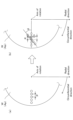
- the radial spacing P of the laser light L can be reduced without changing the branching pitch of the branched laser light L in the branching element by rotating the extension direction of the array of branched laser light L, which forms a line distribution, from the radial direction of the first wafer W (see ⁇ in the figure).
- the radial spacing P of the laser light L can be precisely controlled by rotating the first and second branching elements 125, 126 about the optical axis by the rotation mechanisms 125a, 126a, improving the degree of freedom of the process.
- the radial spacing P when the radial spacing P is controlled by rotating the first and second branching elements 125, 126 around the optical axis in this manner, it is known that the radial spacing P narrows at the same circumferential position depending on the radial position of the laser absorption layer Ap to which the laser light L is irradiated, as shown in FIG. 16 (see radial spacings P1 to P6 in the figure: P1 ⁇ P3 ⁇ P6).
- an appropriate radial spacing P cannot be secured between the irradiation point located at the innermost radial position and the adjacent irradiation point. That is, for example, in the example shown in FIG. 16, the radial spacing P1 becomes smaller than the area affected by the heat effect caused by the irradiation of the laser light, and as a result, there is a risk that the heat effect will overlap between radially adjacent irradiation points.
- the second branching element 126 having a large number of branches of the laser light L is arranged on the optical path. In this way, one laser light L is branched into a plurality of branched laser lights L, and these are irradiated to the laser absorption layer Ap at the same time, thereby shortening the processing time for irradiating the entire surface of the outer peripheral region R1 with the laser light L and improving the throughput.
- a first branching element 125 having a small number of branches of the laser light L is arranged on the optical path. This makes it possible to improve throughput by simultaneously irradiating the laser absorption layer Ap with a plurality of branched laser lights L, while appropriately maintaining the radial spacing P and suppressing overlapping of thermal effects at adjacent irradiation points.
- the arrangement direction of the irradiation points of the laser beam L may be rotated relative to the radial direction of the first wafer W.
- the radial interval P of the laser beam L can be adjusted to an interval shorter than the interval that can be adjusted by the branching by the first and second branching elements 125, 126, thereby further improving the flexibility of the process.
- the end point of the processing of the laser light L may be set with a slight gap in the circumferential direction from the start point of the processing.
- the laser light L is not irradiated to this gap, and the first wafer W and the laser absorbing layer Ap are not peeled off, so that the peeling is more difficult than in the portion irradiated with the laser light L. If this gap is formed in line with the circumferential direction of the laser absorbing layer Ap, there is a risk that peeling will not be performed appropriately at the same circumferential position.
- the number of branches of the laser light L is changed according to predetermined regions (peripheral region R1, central region R2, and central region R3), and further, the first and second branching elements 125, 126 are rotated by the rotation mechanisms 125a, 126a to rotate the arrangement direction of the irradiation points of the laser light L relative to the radial direction of the first wafer W.
- the interval (particularly the radial interval P) between the focusing points of the laser light L can be appropriately controlled only by rotating the first and second branching elements 125, 126 by the rotating mechanisms 125a, 126a without changing the number of branches of the laser light L.
- the interval between the focusing points may be controlled only by rotating the branching elements by the rotating mechanisms 125a, 126a without moving the branching elements in and out of the optical path by the moving mechanisms 125b, 126b during wafer processing.
- the method of irradiating the laser light L disclosed herein is applied when performing laser lift-off to peel off the first wafer W from the laser absorption layer Ap, but the wafer processing to which the method is applicable is not limited to this.
- a modified layer is formed inside a silicon substrate of a wafer having a surface on which multiple devices such as electronic circuits are formed by irradiating the inside of the substrate with laser light along the surface direction, and the wafer is then separated at the modified layer to thin the wafer.
- YAG laser light is used for this laser light.
- the laser light irradiation method disclosed herein can also be applied when forming a modified layer in this manner.
- the laser light irradiation method described above can also be applied to laser devices other than the laser irradiation device disclosed in this disclosure, and can also be applied, for example, to techniques for modifying the surface of a wafer or flattening the surface of a wafer.
- the outer peripheral region R1, the central region R2, and the central region R3 are determined in advance prior to the wafer processing by the laser irradiation device 31.
- these regions may be determined prior to the wafer processing based on a processing limit (a limit point at which the irradiation interval can be controlled by the irradiation conditions of a certain laser light L) determined by the pulse interval in the laser irradiation device 31 and the rotation speed of the chuck 100.
- the number of regions defined in the laser absorption layer Ap is not limited to three and may be defined as four or more based on, for example, the number of branches of the laser light L that can be controlled by the laser irradiation unit 110.
- Laser irradiation device 100 Chuck 110 Laser irradiation unit 111 Laser head 112 Optical system 125 First branching element 125b Movement mechanism 126 Second branching element 126b Movement mechanism L Laser light T Overlapped wafer
Landscapes
- Physics & Mathematics (AREA)
- Optics & Photonics (AREA)
- Engineering & Computer Science (AREA)
- Plasma & Fusion (AREA)
- Mechanical Engineering (AREA)
- Laser Beam Processing (AREA)
Priority Applications (3)
| Application Number | Priority Date | Filing Date | Title |
|---|---|---|---|
| CN202480032016.2A CN121219097A (zh) | 2023-05-25 | 2024-05-13 | 基板处理方法和基板处理装置 |
| JP2025522321A JPWO2024241936A1 (https=) | 2023-05-25 | 2024-05-13 | |
| KR1020257042373A KR20260016511A (ko) | 2023-05-25 | 2024-05-13 | 기판 처리 방법 및 기판 처리 장치 |
Applications Claiming Priority (2)
| Application Number | Priority Date | Filing Date | Title |
|---|---|---|---|
| JP2023-086028 | 2023-05-25 | ||
| JP2023086028 | 2023-05-25 |
Publications (1)
| Publication Number | Publication Date |
|---|---|
| WO2024241936A1 true WO2024241936A1 (ja) | 2024-11-28 |
Family
ID=93589181
Family Applications (1)
| Application Number | Title | Priority Date | Filing Date |
|---|---|---|---|
| PCT/JP2024/017598 Ceased WO2024241936A1 (ja) | 2023-05-25 | 2024-05-13 | 基板処理方法及び基板処理装置 |
Country Status (5)
| Country | Link |
|---|---|
| JP (1) | JPWO2024241936A1 (https=) |
| KR (1) | KR20260016511A (https=) |
| CN (1) | CN121219097A (https=) |
| TW (1) | TW202513208A (https=) |
| WO (1) | WO2024241936A1 (https=) |
Citations (5)
| Publication number | Priority date | Publication date | Assignee | Title |
|---|---|---|---|---|
| JP2000005893A (ja) * | 1998-06-26 | 2000-01-11 | Mitsubishi Heavy Ind Ltd | レーザ加工装置 |
| JP2006281268A (ja) * | 2005-03-31 | 2006-10-19 | Hitachi Via Mechanics Ltd | レーザ加工機 |
| JP2007190560A (ja) * | 2006-01-17 | 2007-08-02 | Miyachi Technos Corp | レーザ加工装置 |
| JP2012170985A (ja) * | 2011-02-22 | 2012-09-10 | Disco Corp | レーザ加工装置 |
| JP2016131997A (ja) * | 2015-01-19 | 2016-07-25 | パナソニックIpマネジメント株式会社 | レーザ切断光学ユニット及びレーザ切断装置 |
Family Cites Families (1)
| Publication number | Priority date | Publication date | Assignee | Title |
|---|---|---|---|---|
| JP7304433B2 (ja) | 2019-12-26 | 2023-07-06 | 東京エレクトロン株式会社 | 基板処理方法及び基板処理装置 |
-
2024
- 2024-05-13 KR KR1020257042373A patent/KR20260016511A/ko active Pending
- 2024-05-13 WO PCT/JP2024/017598 patent/WO2024241936A1/ja not_active Ceased
- 2024-05-13 CN CN202480032016.2A patent/CN121219097A/zh active Pending
- 2024-05-13 JP JP2025522321A patent/JPWO2024241936A1/ja active Pending
- 2024-05-16 TW TW113118121A patent/TW202513208A/zh unknown
Patent Citations (5)
| Publication number | Priority date | Publication date | Assignee | Title |
|---|---|---|---|---|
| JP2000005893A (ja) * | 1998-06-26 | 2000-01-11 | Mitsubishi Heavy Ind Ltd | レーザ加工装置 |
| JP2006281268A (ja) * | 2005-03-31 | 2006-10-19 | Hitachi Via Mechanics Ltd | レーザ加工機 |
| JP2007190560A (ja) * | 2006-01-17 | 2007-08-02 | Miyachi Technos Corp | レーザ加工装置 |
| JP2012170985A (ja) * | 2011-02-22 | 2012-09-10 | Disco Corp | レーザ加工装置 |
| JP2016131997A (ja) * | 2015-01-19 | 2016-07-25 | パナソニックIpマネジメント株式会社 | レーザ切断光学ユニット及びレーザ切断装置 |
Also Published As
| Publication number | Publication date |
|---|---|
| JPWO2024241936A1 (https=) | 2024-11-28 |
| CN121219097A (zh) | 2025-12-26 |
| TW202513208A (zh) | 2025-04-01 |
| KR20260016511A (ko) | 2026-02-03 |
Similar Documents
| Publication | Publication Date | Title |
|---|---|---|
| JP7641434B2 (ja) | 基板処理方法、基板処理装置及び基板処理システム | |
| JP7499845B2 (ja) | 基板処理方法及び基板処理装置 | |
| KR20240163700A (ko) | 기판 처리 장치 및 기판 처리 방법 | |
| WO2024241936A1 (ja) | 基板処理方法及び基板処理装置 | |
| JP7285151B2 (ja) | 支持体剥離方法及び支持体剥離システム | |
| JP7781185B2 (ja) | 基板処理方法及び基板処理装置 | |
| JP7808697B2 (ja) | 基板処理装置及び基板処理方法 | |
| JP7815447B2 (ja) | 基板処理システム、基板処理方法及びデバイス構造 | |
| WO2026034066A1 (ja) | 基板処理システム及び基板処理方法 | |
| WO2026004649A1 (ja) | 基板処理システム、基板処理方法、プログラム及び記憶媒体 | |
| WO2026004650A1 (ja) | 基板処理システム、基板処理方法、プログラム及び記憶媒体 |
Legal Events
| Date | Code | Title | Description |
|---|---|---|---|
| 121 | Ep: the epo has been informed by wipo that ep was designated in this application |
Ref document number: 24810943 Country of ref document: EP Kind code of ref document: A1 |
|
| ENP | Entry into the national phase |
Ref document number: 2025522321 Country of ref document: JP Kind code of ref document: A |
|
| WWE | Wipo information: entry into national phase |
Ref document number: 1020257042373 Country of ref document: KR |
|
| NENP | Non-entry into the national phase |
Ref country code: DE |
|
| WWP | Wipo information: published in national office |
Ref document number: 1020257042373 Country of ref document: KR |