WO2024236770A1 - 切削工具 - Google Patents
切削工具 Download PDFInfo
- Publication number
- WO2024236770A1 WO2024236770A1 PCT/JP2023/018431 JP2023018431W WO2024236770A1 WO 2024236770 A1 WO2024236770 A1 WO 2024236770A1 JP 2023018431 W JP2023018431 W JP 2023018431W WO 2024236770 A1 WO2024236770 A1 WO 2024236770A1
- Authority
- WO
- WIPO (PCT)
- Prior art keywords
- layer
- unit
- less
- unit layer
- thickness
- Prior art date
- Legal status (The legal status is an assumption and is not a legal conclusion. Google has not performed a legal analysis and makes no representation as to the accuracy of the status listed.)
- Ceased
Links
Images






Classifications
-
- B—PERFORMING OPERATIONS; TRANSPORTING
- B23—MACHINE TOOLS; METAL-WORKING NOT OTHERWISE PROVIDED FOR
- B23B—TURNING; BORING
- B23B27/00—Tools for turning or boring machines; Tools of a similar kind in general; Accessories therefor
- B23B27/14—Cutting tools of which the bits or tips or cutting inserts are of special material
- B23B27/148—Composition of the cutting inserts
-
- B—PERFORMING OPERATIONS; TRANSPORTING
- B23—MACHINE TOOLS; METAL-WORKING NOT OTHERWISE PROVIDED FOR
- B23B—TURNING; BORING
- B23B27/00—Tools for turning or boring machines; Tools of a similar kind in general; Accessories therefor
- B23B27/14—Cutting tools of which the bits or tips or cutting inserts are of special material
-
- B—PERFORMING OPERATIONS; TRANSPORTING
- B23—MACHINE TOOLS; METAL-WORKING NOT OTHERWISE PROVIDED FOR
- B23C—MILLING
- B23C5/00—Milling-cutters
- B23C5/16—Milling-cutters characterised by physical features other than shape
-
- C—CHEMISTRY; METALLURGY
- C23—COATING METALLIC MATERIAL; COATING MATERIAL WITH METALLIC MATERIAL; CHEMICAL SURFACE TREATMENT; DIFFUSION TREATMENT OF METALLIC MATERIAL; COATING BY VACUUM EVAPORATION, BY SPUTTERING, BY ION IMPLANTATION OR BY CHEMICAL VAPOUR DEPOSITION, IN GENERAL; INHIBITING CORROSION OF METALLIC MATERIAL OR INCRUSTATION IN GENERAL
- C23C—COATING METALLIC MATERIAL; COATING MATERIAL WITH METALLIC MATERIAL; SURFACE TREATMENT OF METALLIC MATERIAL BY DIFFUSION INTO THE SURFACE, BY CHEMICAL CONVERSION OR SUBSTITUTION; COATING BY VACUUM EVAPORATION, BY SPUTTERING, BY ION IMPLANTATION OR BY CHEMICAL VAPOUR DEPOSITION, IN GENERAL
- C23C14/00—Coating by vacuum evaporation, by sputtering or by ion implantation of the coating forming material
- C23C14/06—Coating by vacuum evaporation, by sputtering or by ion implantation of the coating forming material characterised by the coating material
- C23C14/0641—Nitrides
-
- C—CHEMISTRY; METALLURGY
- C23—COATING METALLIC MATERIAL; COATING MATERIAL WITH METALLIC MATERIAL; CHEMICAL SURFACE TREATMENT; DIFFUSION TREATMENT OF METALLIC MATERIAL; COATING BY VACUUM EVAPORATION, BY SPUTTERING, BY ION IMPLANTATION OR BY CHEMICAL VAPOUR DEPOSITION, IN GENERAL; INHIBITING CORROSION OF METALLIC MATERIAL OR INCRUSTATION IN GENERAL
- C23C—COATING METALLIC MATERIAL; COATING MATERIAL WITH METALLIC MATERIAL; SURFACE TREATMENT OF METALLIC MATERIAL BY DIFFUSION INTO THE SURFACE, BY CHEMICAL CONVERSION OR SUBSTITUTION; COATING BY VACUUM EVAPORATION, BY SPUTTERING, BY ION IMPLANTATION OR BY CHEMICAL VAPOUR DEPOSITION, IN GENERAL
- C23C14/00—Coating by vacuum evaporation, by sputtering or by ion implantation of the coating forming material
- C23C14/06—Coating by vacuum evaporation, by sputtering or by ion implantation of the coating forming material characterised by the coating material
- C23C14/0664—Carbonitrides
-
- C—CHEMISTRY; METALLURGY
- C23—COATING METALLIC MATERIAL; COATING MATERIAL WITH METALLIC MATERIAL; CHEMICAL SURFACE TREATMENT; DIFFUSION TREATMENT OF METALLIC MATERIAL; COATING BY VACUUM EVAPORATION, BY SPUTTERING, BY ION IMPLANTATION OR BY CHEMICAL VAPOUR DEPOSITION, IN GENERAL; INHIBITING CORROSION OF METALLIC MATERIAL OR INCRUSTATION IN GENERAL
- C23C—COATING METALLIC MATERIAL; COATING MATERIAL WITH METALLIC MATERIAL; SURFACE TREATMENT OF METALLIC MATERIAL BY DIFFUSION INTO THE SURFACE, BY CHEMICAL CONVERSION OR SUBSTITUTION; COATING BY VACUUM EVAPORATION, BY SPUTTERING, BY ION IMPLANTATION OR BY CHEMICAL VAPOUR DEPOSITION, IN GENERAL
- C23C14/00—Coating by vacuum evaporation, by sputtering or by ion implantation of the coating forming material
- C23C14/22—Coating by vacuum evaporation, by sputtering or by ion implantation of the coating forming material characterised by the process of coating
- C23C14/24—Vacuum evaporation
- C23C14/32—Vacuum evaporation by explosion; by evaporation and subsequent ionisation of the vapours, e.g. ion-plating
- C23C14/325—Electric arc evaporation
-
- C—CHEMISTRY; METALLURGY
- C23—COATING METALLIC MATERIAL; COATING MATERIAL WITH METALLIC MATERIAL; CHEMICAL SURFACE TREATMENT; DIFFUSION TREATMENT OF METALLIC MATERIAL; COATING BY VACUUM EVAPORATION, BY SPUTTERING, BY ION IMPLANTATION OR BY CHEMICAL VAPOUR DEPOSITION, IN GENERAL; INHIBITING CORROSION OF METALLIC MATERIAL OR INCRUSTATION IN GENERAL
- C23C—COATING METALLIC MATERIAL; COATING MATERIAL WITH METALLIC MATERIAL; SURFACE TREATMENT OF METALLIC MATERIAL BY DIFFUSION INTO THE SURFACE, BY CHEMICAL CONVERSION OR SUBSTITUTION; COATING BY VACUUM EVAPORATION, BY SPUTTERING, BY ION IMPLANTATION OR BY CHEMICAL VAPOUR DEPOSITION, IN GENERAL
- C23C16/00—Chemical coating by decomposition of gaseous compounds, without leaving reaction products of surface material in the coating, i.e. chemical vapour deposition [CVD] processes
- C23C16/22—Chemical coating by decomposition of gaseous compounds, without leaving reaction products of surface material in the coating, i.e. chemical vapour deposition [CVD] processes characterised by the deposition of inorganic material, other than metallic material
- C23C16/30—Deposition of compounds, mixtures or solid solutions, e.g. borides, carbides, nitrides
- C23C16/34—Nitrides
-
- C—CHEMISTRY; METALLURGY
- C23—COATING METALLIC MATERIAL; COATING MATERIAL WITH METALLIC MATERIAL; CHEMICAL SURFACE TREATMENT; DIFFUSION TREATMENT OF METALLIC MATERIAL; COATING BY VACUUM EVAPORATION, BY SPUTTERING, BY ION IMPLANTATION OR BY CHEMICAL VAPOUR DEPOSITION, IN GENERAL; INHIBITING CORROSION OF METALLIC MATERIAL OR INCRUSTATION IN GENERAL
- C23C—COATING METALLIC MATERIAL; COATING MATERIAL WITH METALLIC MATERIAL; SURFACE TREATMENT OF METALLIC MATERIAL BY DIFFUSION INTO THE SURFACE, BY CHEMICAL CONVERSION OR SUBSTITUTION; COATING BY VACUUM EVAPORATION, BY SPUTTERING, BY ION IMPLANTATION OR BY CHEMICAL VAPOUR DEPOSITION, IN GENERAL
- C23C16/00—Chemical coating by decomposition of gaseous compounds, without leaving reaction products of surface material in the coating, i.e. chemical vapour deposition [CVD] processes
- C23C16/22—Chemical coating by decomposition of gaseous compounds, without leaving reaction products of surface material in the coating, i.e. chemical vapour deposition [CVD] processes characterised by the deposition of inorganic material, other than metallic material
- C23C16/30—Deposition of compounds, mixtures or solid solutions, e.g. borides, carbides, nitrides
- C23C16/36—Carbonitrides
-
- C—CHEMISTRY; METALLURGY
- C23—COATING METALLIC MATERIAL; COATING MATERIAL WITH METALLIC MATERIAL; CHEMICAL SURFACE TREATMENT; DIFFUSION TREATMENT OF METALLIC MATERIAL; COATING BY VACUUM EVAPORATION, BY SPUTTERING, BY ION IMPLANTATION OR BY CHEMICAL VAPOUR DEPOSITION, IN GENERAL; INHIBITING CORROSION OF METALLIC MATERIAL OR INCRUSTATION IN GENERAL
- C23C—COATING METALLIC MATERIAL; COATING MATERIAL WITH METALLIC MATERIAL; SURFACE TREATMENT OF METALLIC MATERIAL BY DIFFUSION INTO THE SURFACE, BY CHEMICAL CONVERSION OR SUBSTITUTION; COATING BY VACUUM EVAPORATION, BY SPUTTERING, BY ION IMPLANTATION OR BY CHEMICAL VAPOUR DEPOSITION, IN GENERAL
- C23C28/00—Coating for obtaining at least two superposed coatings either by methods not provided for in a single one of groups C23C2/00 - C23C26/00 or by combinations of methods provided for in subclasses C23C and C25C or C25D
- C23C28/04—Coating for obtaining at least two superposed coatings either by methods not provided for in a single one of groups C23C2/00 - C23C26/00 or by combinations of methods provided for in subclasses C23C and C25C or C25D only coatings of inorganic non-metallic material
- C23C28/042—Coating for obtaining at least two superposed coatings either by methods not provided for in a single one of groups C23C2/00 - C23C26/00 or by combinations of methods provided for in subclasses C23C and C25C or C25D only coatings of inorganic non-metallic material including a refractory ceramic layer, e.g. refractory metal oxides, ZrO2, rare earth oxides
-
- C—CHEMISTRY; METALLURGY
- C23—COATING METALLIC MATERIAL; COATING MATERIAL WITH METALLIC MATERIAL; CHEMICAL SURFACE TREATMENT; DIFFUSION TREATMENT OF METALLIC MATERIAL; COATING BY VACUUM EVAPORATION, BY SPUTTERING, BY ION IMPLANTATION OR BY CHEMICAL VAPOUR DEPOSITION, IN GENERAL; INHIBITING CORROSION OF METALLIC MATERIAL OR INCRUSTATION IN GENERAL
- C23C—COATING METALLIC MATERIAL; COATING MATERIAL WITH METALLIC MATERIAL; SURFACE TREATMENT OF METALLIC MATERIAL BY DIFFUSION INTO THE SURFACE, BY CHEMICAL CONVERSION OR SUBSTITUTION; COATING BY VACUUM EVAPORATION, BY SPUTTERING, BY ION IMPLANTATION OR BY CHEMICAL VAPOUR DEPOSITION, IN GENERAL
- C23C28/00—Coating for obtaining at least two superposed coatings either by methods not provided for in a single one of groups C23C2/00 - C23C26/00 or by combinations of methods provided for in subclasses C23C and C25C or C25D
- C23C28/04—Coating for obtaining at least two superposed coatings either by methods not provided for in a single one of groups C23C2/00 - C23C26/00 or by combinations of methods provided for in subclasses C23C and C25C or C25D only coatings of inorganic non-metallic material
- C23C28/044—Coating for obtaining at least two superposed coatings either by methods not provided for in a single one of groups C23C2/00 - C23C26/00 or by combinations of methods provided for in subclasses C23C and C25C or C25D only coatings of inorganic non-metallic material coatings specially adapted for cutting tools or wear applications
-
- C—CHEMISTRY; METALLURGY
- C23—COATING METALLIC MATERIAL; COATING MATERIAL WITH METALLIC MATERIAL; CHEMICAL SURFACE TREATMENT; DIFFUSION TREATMENT OF METALLIC MATERIAL; COATING BY VACUUM EVAPORATION, BY SPUTTERING, BY ION IMPLANTATION OR BY CHEMICAL VAPOUR DEPOSITION, IN GENERAL; INHIBITING CORROSION OF METALLIC MATERIAL OR INCRUSTATION IN GENERAL
- C23C—COATING METALLIC MATERIAL; COATING MATERIAL WITH METALLIC MATERIAL; SURFACE TREATMENT OF METALLIC MATERIAL BY DIFFUSION INTO THE SURFACE, BY CHEMICAL CONVERSION OR SUBSTITUTION; COATING BY VACUUM EVAPORATION, BY SPUTTERING, BY ION IMPLANTATION OR BY CHEMICAL VAPOUR DEPOSITION, IN GENERAL
- C23C28/00—Coating for obtaining at least two superposed coatings either by methods not provided for in a single one of groups C23C2/00 - C23C26/00 or by combinations of methods provided for in subclasses C23C and C25C or C25D
- C23C28/40—Coatings including alternating layers following a pattern, a periodic or defined repetition
- C23C28/42—Coatings including alternating layers following a pattern, a periodic or defined repetition characterized by the composition of the alternating layers
-
- C—CHEMISTRY; METALLURGY
- C23—COATING METALLIC MATERIAL; COATING MATERIAL WITH METALLIC MATERIAL; CHEMICAL SURFACE TREATMENT; DIFFUSION TREATMENT OF METALLIC MATERIAL; COATING BY VACUUM EVAPORATION, BY SPUTTERING, BY ION IMPLANTATION OR BY CHEMICAL VAPOUR DEPOSITION, IN GENERAL; INHIBITING CORROSION OF METALLIC MATERIAL OR INCRUSTATION IN GENERAL
- C23C—COATING METALLIC MATERIAL; COATING MATERIAL WITH METALLIC MATERIAL; SURFACE TREATMENT OF METALLIC MATERIAL BY DIFFUSION INTO THE SURFACE, BY CHEMICAL CONVERSION OR SUBSTITUTION; COATING BY VACUUM EVAPORATION, BY SPUTTERING, BY ION IMPLANTATION OR BY CHEMICAL VAPOUR DEPOSITION, IN GENERAL
- C23C30/00—Coating with metallic material characterised only by the composition of the metallic material, i.e. not characterised by the coating process
- C23C30/005—Coating with metallic material characterised only by the composition of the metallic material, i.e. not characterised by the coating process on hard metal substrates
-
- B—PERFORMING OPERATIONS; TRANSPORTING
- B23—MACHINE TOOLS; METAL-WORKING NOT OTHERWISE PROVIDED FOR
- B23B—TURNING; BORING
- B23B2228/00—Properties of materials of tools or workpieces, materials of tools or workpieces applied in a specific manner
- B23B2228/10—Coatings
- B23B2228/105—Coatings with specified thickness
Definitions
- This disclosure relates to cutting tools.
- Patent Document 1 cutting tools that have a substrate and a coating disposed on the substrate have been used for cutting.
- a cutting tool includes: 1.
- a cutting tool comprising a substrate and a coating disposed on the substrate, The coating comprises a first layer, The first layer is composed of alternating layers in which first unit layers and second unit layers are alternately laminated, the first unit layer has a hexagonal crystal structure, The first unit layer is made of W(C 1-a N a ) x ; The a is 0.3 or more and 0.8 or less, The x is 0.8 or more and 1.2 or less, the second unit layer is made of Al c V 1-c N; The cutting tool, wherein c is equal to or greater than 0.40 and equal to or less than 0.80.
- FIG. 1 is a schematic enlarged cross-sectional view of an example of a cutting tool according to a first embodiment.
- FIG. 2 is a schematic enlarged cross-sectional view of another example of the cutting tool according to the first embodiment.
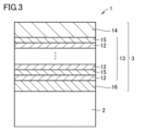
- FIG. 3 is a schematic enlarged cross-sectional view of another example of the cutting tool according to the first embodiment.
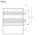
- FIG. 4 is a schematic enlarged cross-sectional view of another example of the cutting tool according to the first embodiment.
- FIG. 5 is a diagram for explaining an example of the ratio of the thickness of the first unit layer to the thickness of the second unit layer.
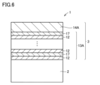
- FIG. 6 is a schematic enlarged cross-sectional view of an example of a cutting tool according to the second embodiment.
- FIG. 1 is a schematic enlarged cross-sectional view of an example of a cutting tool according to a first embodiment.
- FIG. 2 is a schematic enlarged cross-sectional view of another example of the cutting tool according to the first embodiment.
- FIG. 3 is a schematic enlarged cross-sectional
- FIG. 7 is a schematic enlarged cross-sectional view of another example of the cutting tool according to the second embodiment.
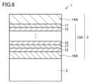
- FIG. 8 is a schematic enlarged cross-sectional view of another example of the cutting tool according to the second embodiment.
- FIG. 9 is a schematic enlarged cross-sectional view of another example of the cutting tool according to the second embodiment.
- FIG. 10 is a diagram for explaining an example of the ratio of the thickness of the first unit layer to the thickness of the third unit layer.
- FIG. 11 is a schematic cross-sectional view of a cathodic arc ion plating apparatus used in the examples.
- FIG. 12 is a schematic top view of the cathodic arc ion plating apparatus shown in FIG.
- Cutting plays a central role in manufacturing technology, and there is a constant demand for technological evolution and further sophistication.
- high speed, high efficiency, high precision machining, and ultra-fine machining are fundamentally required.
- a recent trend is that work materials are becoming more difficult to cut, and there is a demand for measures to address this.
- attention has been increasingly being paid to the SDGs (Sustainable Development Goals) in recent years in order to realize a sustainable and better world by 2030.
- Sustainable development means building a social infrastructure that can withstand the threats of nature without compromising the resources needed by future generations.
- Patent Document 1 A nitride film mainly composed of Al and V has been proposed as a coating tool material (Patent Document 1). From the viewpoint of SDGs and global environmental conservation, dry machining without the use of cutting oil is required, cutting speeds are becoming faster to improve machining efficiency, and work materials are becoming more diverse, with cutting of heat-resistant alloys and titanium alloys, which are known as difficult-to-cut materials, increasing in particular in the aircraft and medical fields. For these reasons, the cutting edge temperature of cutting tools during cutting tends to become high. If the cutting edge temperature becomes high, the life of the cutting tool will be extremely shortened. Therefore, there is a demand for cutting tools that can demonstrate excellent tool life even under such harsh cutting conditions.
- a cutting tool comprising a substrate and a coating disposed on the substrate, The coating comprises a first layer, The first layer is composed of alternating layers in which first unit layers and second unit layers are alternately laminated, the first unit layer has a hexagonal crystal structure, The first unit layer is made of W(C 1-a N a ) x ; The a is 0.3 or more and 0.8 or less, The x is 0.8 or more and 1.2 or less, the second unit layer is made of Al c V 1-c N; The cutting tool, wherein c is equal to or greater than 0.40 and equal to or less than 0.80.
- This disclosure makes it possible to provide cutting tools that have a long tool life, especially in cutting processes that are performed under conditions of high cutting edge temperatures.
- the ratio ⁇ 2/ ⁇ 1 of the thickness ⁇ 2 ⁇ m of the second unit layer to the thickness ⁇ 1 ⁇ m of the first unit layer in the first unit layer and the second unit layer adjacent to the first unit layer may be 1.0 or more and 5.0 or less. This allows the cutting tool to have a longer tool life.
- the first unit layer has an average thickness of 0.002 ⁇ m or more and 0.2 ⁇ m or less
- the second unit layer may have an average thickness of 0.002 ⁇ m or more and 0.2 ⁇ m or less. This allows the cutting tool to have a longer tool life.
- the coating further includes a second layer disposed between the substrate and the first layer;
- the composition of the second layer may be the same as the composition of the first unit layer or the composition of the second unit layer. This allows the cutting tool to have a longer tool life.
- the composition of the second layer is the same as the composition of the first unit layer;
- the second layer may have a thickness greater than that of the first unit layer. This allows the cutting tool to have a longer tool life.
- the composition of the second layer is the same as the composition of the second unit layer;
- the second layer may have a thickness greater than a thickness of the second unit layer. This allows the cutting tool to have a longer tool life.
- the coating further includes a third layer provided on a side of the first layer opposite the substrate,
- the third layer may be made of AlVCN. This allows the cutting tool to have a longer tool life.
- a cutting tool comprising a substrate and a coating disposed on the substrate, The coating comprises a first A layer, The first A layer is composed of alternating layers in which first unit layers and third unit layers are alternately laminated, the first unit layer has a hexagonal crystal structure, The first unit layer is made of W(C 1-a N a ) x ; The a is 0.3 or more and 0.8 or less, The x is 0.8 or more and 1.2 or less, The third unit layer is made of Al d V 1-de Me N , M is silicon, boron, yttrium, cerium or lanthanum; The d is 0.40 or more and 0.80 or less, The cutting tool, wherein e is greater than 0 and is 0.05 or less.
- This disclosure makes it possible to provide cutting tools that have a long tool life, especially in cutting processes that are performed under conditions of high cutting edge temperatures.
- a ratio ⁇ 3/ ⁇ 1 of the thickness ⁇ 3 ⁇ m of the third unit layer to the thickness ⁇ 1 ⁇ m of the first unit layer may be 1.0 or more and 5.0 or less. This allows the cutting tool to have a longer tool life.
- the M may be silicon. This allows the cutting tool to have a longer tool life.
- the M may be boron. This allows the cutting tool to have a longer tool life.
- the first unit layer has an average thickness of 0.002 ⁇ m or more and 0.2 ⁇ m or less
- the third unit layer may have an average thickness of 0.002 ⁇ m or more and 0.2 ⁇ m or less. This allows the cutting tool to have a longer tool life.
- the coating further includes a second A layer disposed between the substrate and the first A layer;
- the composition of the second A layer may be the same as the composition of the first unit layer or the composition of the third unit layer. This allows the cutting tool to have a longer tool life.
- composition of the second A layer is the same as the composition of the first unit layer,
- the second A layer may have a thickness greater than that of the first unit layer. This allows the cutting tool to have a longer tool life.
- composition of the second A layer is the same as the composition of the third unit layer,
- the second A layer may have a thickness greater than that of the third unit layer. This allows the cutting tool to have a longer tool life.
- the coating further includes a third A layer provided on the side of the first A layer opposite the substrate, the 3A layer is made of AlVMeCN,
- the Me may be silicon, boron, yttrium, cerium or lanthanum. This allows the cutting tool to have a longer tool life.
- a ⁇ B means the upper and lower limits of a range (i.e., greater than or equal to A and less than or equal to B). If no unit is stated for A and only a unit is stated for B, the units of A and B are the same.
- any one numerical value listed as the lower limit and any one numerical value listed as the upper limit is also considered to be disclosed.
- a1 or more, b1 or more, and c1 or more are listed as the lower limit and a2 or less, b2 or less, and c2 or less are listed as the upper limit, a1 or more and a2 or less, a1 or more and b2 or less, a1 or more and c2 or less, b1 or more and a2 or less, b1 or more and b2 or less, b1 or more and c2 or less, c1 or more and a2 or less, c1 or more and b2 or less, and c1 or more and c2 or less are considered to be disclosed.
- FIG. A cutting tool 1 according to one embodiment of the present disclosure includes: A cutting tool comprising a substrate 2 and a coating 3 disposed on the substrate 2, The coating 3 includes a first layer 13, The first layer 13 is composed of alternating layers in which the first unit layers 12 and the second unit layers 15 are alternately laminated, The first unit layer 12 has a hexagonal crystal structure, The first unit layer 12 is made of W(C 1-a N a ) x ; a is equal to or greater than 0.3 and equal to or less than 0.8, x is equal to or greater than 0.8 and equal to or less than 1.2; The second unit layer 15 is made of Al c V 1-c N, The cutting tool has a coefficient of friction coefficient c that is greater than or equal to 0.40 and less than or equal to 0.80.
- the cutting tool 1 of the first embodiment has a long tool life, especially in cutting operations performed under conditions of high cutting edge temperatures. The reasons for this are presumed to be as follows.
- the first unit layer 12 is made of W(C 1-a N a ) x . Since the first unit layer 12 contains C (carbon), the friction coefficient at the contact interface with the workpiece is reduced, and cutting resistance can be reduced. In addition, since W(C 1-a N a ) x contains N (nitrogen), heat resistance is improved by about 150°C compared to WC. As a result, the first layer including the first unit layer can improve adhesion resistance, sliding properties, and wear resistance in processing where the cutting edge becomes hot, such as during dry cutting processing. Therefore, the cutting tool including the first layer has an improved tool life.
- the second unit layer 15 is made of Al c V 1-c N.
- the second unit layer 15 contains Al. Since Al is easily oxidized, a dense oxide layer made of Al 2 O 3 tends to be easily formed on the surface side of the first layer 13 in the coating including the second unit layer 12. As a result, the heat barrier property and oxidation resistance of the first layer 13 can be improved. Therefore, the tool life of a cutting tool including the first layer 13 is improved.
- the second unit layer 15 is oxidized during cutting to produce V2O5 , an oxide of V. Since the melting point of V2O5 is 690°C, it softens at the temperature during cutting and functions as a lubricant, thereby reducing the coefficient of friction on the rake face of the tool.
- the first layer 13 is made up of alternating layers in which first unit layers 12 and second unit layers 15 are alternately stacked.
- the composition and crystal lattice are discontinuous at the interface between the first unit layers 12 and the second unit layers 15. Therefore, if a crack occurs on the surface of the coating 3 during cutting, the crack can be prevented from progressing at the interface. In a coating that includes the first layer, chipping and loss are prevented. Therefore, a cutting tool that includes the first layer 13 has an improved tool life.
- a cutting tool 1 includes a substrate 2 and a coating 3 disposed on the substrate 2.
- the coating 3 can cover at least a portion of the substrate 2 involved in cutting.
- the coating 3 may cover the entire surface of the substrate 2. Even if the configuration of the coating 3 is partially different, it does not deviate from the scope of this embodiment.
- the portion of the substrate 2 involved in cutting refers to an area on the surface of the substrate 2 that is at least within 50 ⁇ m, 100 ⁇ m, or 300 ⁇ m away from the cutting edge.
- the cutting tool 1 of this embodiment can be suitably used as a cutting tool 1 such as a drill, an end mill, an indexable cutting tip for a drill, an indexable cutting tip for an end mill, an indexable cutting tip for milling, an indexable cutting tip for turning, a metal saw, a gear cutting tool, a reamer, and a tap.
- a cutting tool 1 such as a drill, an end mill, an indexable cutting tip for a drill, an indexable cutting tip for an end mill, an indexable cutting tip for milling, an indexable cutting tip for turning, a metal saw, a gear cutting tool, a reamer, and a tap.
- the substrate 2 may be made of any of cemented carbide (WC-based cemented carbide, cemented carbide containing WC and Co, cemented carbide containing WC and Co with carbonitrides of Ti, Ta, Nb, etc.), cermet (mainly composed of TiC, TiN, TiCN, etc.), high-speed steel, ceramics (titanium carbide, silicon carbide, silicon nitride, aluminum nitride, aluminum oxide, etc.), cubic boron nitride sintered body, and diamond sintered body.
- cemented carbide WC-based cemented carbide, cemented carbide containing WC and Co, cemented carbide containing WC and Co with carbonitrides of Ti, Ta, Nb, etc.
- cermet mainly composed of TiC, TiN, TiCN, etc.
- high-speed steel ceramics (titanium carbide, silicon carbide, silicon nitride, aluminum nitride, aluminum oxide, etc.), cubic boron nit
- the substrate 2 may be, in particular, a WC-based cemented carbide or a cermet (particularly a TiCN-based cermet).
- WC-based cemented carbide or a cermet has an excellent balance of hardness and strength, particularly at high temperatures, and therefore, when used as the substrate 2 of the cutting tool 1, can contribute to extending the life of the cutting tool 1.
- the coating 3 of the first embodiment includes a first layer 13.
- the coating 3 covers the substrate 2, thereby improving various properties of the cutting tool 1, such as wear resistance and chipping resistance, and has the effect of extending the life of the cutting tool 1.
- the coating 3 may include other layers in addition to the first layer 13. As shown in Figures 3 and 4, the other layers include a second layer 16 disposed between the substrate 2 and the first layer 13, and a third layer 14 disposed on the side of the first layer 13 opposite the substrate 2.
- the coating 3 may have a total thickness of 0.4 ⁇ m or more and 15 ⁇ m or less. If the total thickness of the coating 3 is 0.4 ⁇ m or more, the effect of extending the life of the cutting tool 1 by providing the coating 3 is easily obtained. On the other hand, if the total thickness of the coating 3 is 15 ⁇ m or less, chipping of the coating 3 is less likely to occur in the early stages of cutting, and the life of the cutting tool 1 can be extended.
- the overall thickness of the coating 3 can be measured by observing a cross section of the coating 3 using a scanning electron microscope (SEM).
- SEM scanning electron microscope
- the specific measurement method is as follows.
- the cutting tool 1 is cut in a direction along the normal to the surface of the coating 3 to prepare a cross section sample.
- the cross section sample is observed with the SEM.
- the observation magnification is 5000 to 10000 times, and the measurement field of view is 100 to 500 ⁇ m2 .
- the thickness width is measured at three points on the coating 3, and the average value of the thickness widths at the three points is calculated. This average value corresponds to the thickness of the coating 3.
- the thickness of each layer described below is also measured in a similar manner unless otherwise specified.
- the compressive residual stress of the coating 3 may have an absolute value of 6 GPa or less.
- the compressive residual stress of the coating 3 is a type of internal stress (intrinsic strain) that exists throughout the coating 3, and is a stress expressed as a "-" (negative) numerical value (unit: "GPa” is used in this embodiment). Therefore, the concept of a large compressive residual stress indicates that the absolute value of the numerical value is large, and the concept of a small compressive residual stress indicates that the absolute value of the numerical value is small.
- the absolute value of the compressive residual stress being 6 GPa or less means that the compressive residual stress of the coating 3 is -6 GPa or more and 0 GPa or less.
- the compressive residual stress of the coating 3 is 0 GPa or less, it is easy to suppress the progression of cracks that occur from the outermost surface of the coating 3.
- the absolute value of the compressive residual stress is 6 GPa or less, the magnitude of the stress is appropriate, and it is easy to suppress peeling of the coating 3 from the edge of the cutting tool 1 before cutting begins.
- the compressive residual stress of the coating 3 is measured by the sin 2 ⁇ method (see pages 54-66 of "X-Ray Stress Measurement Method” (published by Yokendo Co., Ltd., 1981, by the Japan Society for Materials Science)) using an X-ray residual stress device.
- the first unit layer 12 can have a hexagonal crystal structure. When the first unit layer 12 has a hexagonal crystal structure, the abrasion resistance of the coating 3 is improved.
- the second unit layer 15 can include a cubic crystal structure. When the second unit layer 15 has a cubic crystal structure, the hardness of the coating 3 is improved.
- the crystal structure of each layer in the coating 3 can be analyzed by an X-ray diffraction device known in the field.
- the hardness of the coating 3 is most effective when it is between 30 GPa and 55 GPa, and may be between 35 GPa and 50 GPa. This means that the coating 3 has sufficient hardness.
- the hardness of the entire coating 3 is measured by a nanoindenter method (Nano Indenter XP manufactured by MTS). Specifically, this is performed using a method conforming to ISO14577, with a measurement load of 10 mN (1 gf), the hardness is measured at three points on the surface of the coating 3, and the average value of the hardness at the three points is calculated. This average value corresponds to the hardness of the coating 3.
- the first layer 13 in this embodiment is composed of alternating layers in which the first unit layers 12 and the second unit layers 15 are alternately stacked.
- the fact that the first layer 13 is composed of alternating layers in which the first unit layers 12 and the second unit layers 15 are alternately stacked can be confirmed by observing a thin sample including a cross section of the coating 3 with a TEM (transmission electron microscope) and observing the difference in contrast.
- Either of the first unit layer 12 and the second unit layer 15 may be disposed in a position closest to the substrate 2.
- the first unit layer 12 is disposed directly on the substrate 2.
- the second unit layer 15 is disposed directly on the substrate 2.
- Either of the first unit layer 12 and the second unit layer 15 may be disposed on the surface side of the coating 3.
- the second unit layer 15 is disposed on the surface side of the coating 3.
- the first unit layer 12 is disposed on the surface side of the coating 3.
- the thickness of the first layer 13 may be 0.5 ⁇ m or more and 15 ⁇ m or less. When the thickness of the first layer 13 is 0.5 ⁇ m or more, it can exhibit excellent wear resistance in continuous processing. When the thickness of the first layer 13 is 15 ⁇ m or less, it can exhibit excellent chipping resistance in intermittent cutting.
- the thickness of the first layer 13 is measured by observing and measuring the cross section of the coating 3 using a transmission electron microscope (TEM).
- TEM transmission electron microscope
- a specific measurement method is as follows.
- the cutting tool 1 is cut in a direction along the normal to the surface of the coating 3 to prepare a thin section sample including the cross section of the coating 3.
- the thin section sample is observed with the TEM.
- the observation magnification is 20,000 to 5,000,000 times, and the measurement field of view is 0.0016 to 80 ⁇ m2 .
- the thickness width of the first layer 13 is measured at three points, and the average value of the thickness widths at the three points is calculated. The average value corresponds to the thickness of the first layer 13.
- the first unit layer 12 may have a hexagonal crystal structure.
- the hexagonal crystal structure is derived from W(C 1-a N a ) x constituting the first unit layer 12. It can be confirmed that the first unit layer 12 has a hexagonal crystal structure by analysis using XRD measurement. When peaks attributable to a hexagonal crystal structure defined by ⁇ -W 2 C (01-076-7103) and W 4.6 N 4 (01-077-2001) of JCPDS (ICDD) are observed in the obtained XRD spectrum, it is confirmed that the first unit layer 12 has a hexagonal crystal structure.
- the coating includes other layers such as the second unit layer 15, the second layer 16, the third layer 14, and an intermediate layer in addition to the first unit layer, and peaks originating from layers other than the first unit layer 12 or from the substrate (hereinafter also referred to as "other peaks") are detected in the XRD spectrum from the surface of the coating 3, it is also possible to identify that the first unit layer 12 has a hexagonal crystal structure.
- An example of an apparatus used for the X-ray diffraction measurement is "SmartLab" (product name) manufactured by Rigaku Corp.
- the conditions for the XRD measurement are as follows. (XRD measurement conditions) Scanning axis: 2 ⁇ - ⁇ X-ray source: Cu-K ⁇ ray (1.541862 ⁇ ) Detector: 0-dimensional detector (scintillation counter) Tube voltage: 45 kV Tube current: 40mA Incident optical system: Use of mirrors Receiving optical system: Use of analyzer crystal (PW3098/27) Step: 0.03° Accumulation time: 2 seconds Scan range (2 ⁇ ): 10° to 120°
- the first unit layer 12 is made of W(C 1-a N a ) x , where a is 0.3 or more and 0.8 or less, and x is 0.8 or more and 1.2 or less, so that the crystal structure of the first unit layer 12 is a hexagonal type, and the heat resistance, oxidation resistance, and wear resistance of the first unit layer 12 can be improved.
- the lower limit of a is 0.3 or more, and may be 0.35 or more, 0.40 or more, or 0.45 or more.
- the upper limit of a is 0.8 or less, and may be 0.75 or less, 0.70 or less, or 0.65 or less.
- a may be 0.35 or more and 0.75 or less, 0.40 or more and 0.70 or less, or 0.45 or more and 0.65 or less.
- the lower limit of x is 0.8 or more, may be 0.85 or more, or may be 0.90 or more.
- the upper limit of x is 1.2 or less, may be 1.15 or less, or may be 1.10 or less.
- x may be 0.85 or more and 1.15 or less, may be 0.90 or more and 1.10 or less, or may be 1.00.
- the first unit layer is made of W(C 1-a N a ) x
- the first unit layer 12 may contain inevitable impurities in addition to W(C 1-a N a ) x , as long as the effect of the present disclosure is not impaired.
- inevitable impurities include oxygen and carbon.
- the total content of inevitable impurities in the first unit layer 12 may be greater than 0 atomic % and less than 1 atomic %.
- atomic % means the ratio (%) of the number of atoms to the total number of atoms constituting the layer.
- the second unit layer 15 is made of Al c V 1-c N, and c is 0.40 or more and 0.80 or less.
- the second unit layer 15 can improve the heat resistance, oxidation resistance, and toughness of the coating 3.
- the lower limit of c is 0.40 or more, and may be 0.45 or more, 0.50 or more, or 0.55 or more.
- the upper limit of c is 0.80 or less, and may be 0.75 or less, 0.70 or less, or 0.65 or less.
- c may be 0.45 or more and 0.75 or less, 0.50 or more and 0.70 or less, or 0.55 or more and 0.65 or less.
- the second unit layer is made of Al c V 1-c N
- the second unit layer 15 may contain inevitable impurities in addition to Al c V 1-c N, as long as the effect of the present disclosure is not impaired.
- the inevitable impurities include oxygen and carbon.
- the total content of the inevitable impurities in the second unit layer 15 may be greater than 0 atomic % and less than 1 atomic %.
- the above a, the above x, the above c, and the content of inevitable impurities in the first unit layer 12 and the content of inevitable impurities in the second unit layer 15 are measured by elemental analysis of the cross section of the coating 3 using a transmission electron microscope (TEM).
- TEM transmission electron microscope
- the specific measurement method is as follows.
- the cutting tool 1 is cut in a direction along the normal line of the surface of the coating 3 to prepare a thin sample including a cross section of the coating 3.
- An electron beam is irradiated onto the thin sample using an EDS (Energy Dispersive X-ray Spectroscopy) attached to the TEM, and the energy and number of characteristic X-rays generated at that time are measured to perform elemental analysis of the first unit layer 12 and the second unit layer 15.
- EDS Electronicgy Dispersive X-ray Spectroscopy
- the average composition of the five first unit layers 12 is determined. This average composition corresponds to the composition of the first unit layer 12.
- the average composition of the five second unit layers 15 is determined. This average composition corresponds to the composition of the second unit layer 15. If the number of layers of each of the first unit layer 12 and the second unit layer 15 is four or less, elemental analysis is performed on all layers to determine the average composition of the first unit layer 12 and the second unit layer 15. As long as the measurements are performed using the same cutting tool 1, it has been confirmed that there is no variation in the measurement results even if the measurement points are selected arbitrarily.
- the ratio A N1 /A M1 of the total number of atoms A N1 of C and N to the number A M1 of atoms of W is 0.8 or more and 1.2 or less.
- the ratio A N2 /A M2 of the number of atoms A N2 of N to the total number A M2 of atoms of Al and V is necessarily 0.8 or more and 1.2 or less in manufacturing.
- the ratios A N1 /A M1 and A N2 /A M2 can be measured by the Rutherford backscattering (RBS) method. It has been confirmed that the effect of the present disclosure is not impaired if the ratios A N1 /A M1 and A N2 /A M2 are within the above ranges.
- the average thickness of the first unit layer 12 may be 0.002 ⁇ m or more and 0.2 ⁇ m or less, and the average thickness of the second unit layer 15 may be 0.002 ⁇ m or more and 0.2 ⁇ m or less. This can further suppress the progression of cracks generated on the surface of the coating 3.
- the lower limit of the average thickness of the first unit layer 12 may be 0.002 ⁇ m or more, 0.005 ⁇ m or more, or 0.01 ⁇ m or more.
- the upper limit of the average thickness of the first unit layer 12 may be 0.20 ⁇ m or less, 0.15 ⁇ m or less, or 0.10 ⁇ m or less.
- the average thickness of the first unit layer 12 may be 0.005 ⁇ m or more and 0.15 ⁇ m or less, or 0.01 ⁇ m or more and 0.1 ⁇ m or less.
- the lower limit of the average thickness of the second unit layer 15 may be 0.002 ⁇ m or more, 0.005 ⁇ m or more, or 0.01 ⁇ m or more.
- the upper limit of the average thickness of the second unit layer 15 may be 0.20 ⁇ m or less, 0.15 ⁇ m or less, or 0.10 ⁇ m or less.
- the average thickness of the second unit layer 15 may be 0.005 ⁇ m or more and 0.15 ⁇ m or less, or 0.01 ⁇ m or more and 0.10 ⁇ m or less.
- the average thickness of the first unit layer 12 and the average thickness of the second unit layer 15 can be measured using a method similar to the method for measuring the thickness of the first layer 13 described above.
- the ratio ⁇ 2/ ⁇ 1 of the thickness ⁇ 2 ⁇ m of the second unit layer 15 to the thickness ⁇ 1 ⁇ m of the first unit layer 12 may be 1.0 or more and 5.0 or less.
- the second unit layer 15 has a low thermal conductivity and is less likely to transmit heat generated during cutting to the substrate 2.
- the ratio ⁇ 2/ ⁇ 1 is 1.0 or more, the proportion of the second unit layer 15 in the coating 3 increases relatively, and the amount of Al in the coating 3 increases, improving the heat insulation of the cutting tool 1 as a whole.
- the cutting tool 1 having the coating 3 has improved wear resistance, especially during continuous cutting.
- ⁇ 2/ ⁇ 1 When ⁇ 2/ ⁇ 1 is 1.0 or more, the toughness of the coating 3 tends to improve. On the other hand, when ⁇ 2/ ⁇ 1 is 5.0 or less, the effect of suppressing crack propagation by stacking the first unit layer 12 and the second unit layer 15 tends to be easily obtained.
- ⁇ 2/ ⁇ 1 may be 1.0 or more, 1.1 or more, 1.2 or more, 1.3 or more, 1.4 or more, 1.5 or more, 2.0 or more, or 2.5 or more.
- ⁇ 2/ ⁇ 1 may be 5.0 or less, 4.0 or less, or 3.0 or less.
- ⁇ 2/ ⁇ 1 may be 1.2 or more and 4.0 or less, or 1.5 or more and 2.5 or less.
- FIG. 1 For the sake of explanation, in FIG.
- the thicknesses of the three first unit layers 12 are all indicated as ⁇ 1
- the thicknesses of the three second unit layers 15 are all indicated as ⁇ 2, but as long as the above ⁇ 2/ ⁇ 1 relationship is satisfied between adjacent first unit layers and second unit layers, the thicknesses ⁇ 1 of the three first unit layers 12 do not need to be the same, and the thicknesses ⁇ 2 of the three second unit layers 15 do not need to be the same.
- the number of layers of each of the first unit layers 12 and the second unit layers 15 may be 5 or more and 500 or less, or may be 10 or more and 500 or less. This allows the effect of improving hardness and compressive residual stress in a well-balanced manner to be sufficiently obtained by stacking the first unit layers 12 and the second unit layers 15.
- the number of layers of each of the first unit layers 12 and the second unit layers 15 may be 100 or more and 400 or less, or may be 200 or more and 350 or less.
- the number of layers of each of the first unit layers 12 and the second unit layers 15 in the first layer 13 can be determined by observing a thin sample of the cross section of the coating 3 using a transmission electron microscope (TEM) at a magnification of 20,000 to 5,000,000 times.
- TEM transmission electron microscope
- the coating 3 further includes a second layer 16 disposed between the substrate 2 and the first layer 13, and the composition of the second layer 16 may be the same as the composition of the first unit layer 12 or the composition of the second unit layer 15. This can increase the adhesion between the substrate 2 and the coating 3.
- the composition of the second layer 16 is the same as that of the first unit layer 12, even if the second layer 16 is exposed at the beginning of cutting, the second layer 16 has good sliding properties, and therefore the wear resistance can be improved.
- the thickness of the second layer 16 may be thicker than that of the first unit layer 12. This can further increase the adhesion between the substrate 2 and the coating 3. In addition, even if the second layer 16 is exposed at the beginning of cutting, the second layer 16 has good sliding properties, so that the wear resistance can be improved. "The thickness of the second layer is thicker than that of the first unit layer" can be rephrased as "The thickness of the second layer is more than 1.0 times the thickness of the first unit layer.” The thickness of the second layer 16 may be 2.0 times or more, 4.0 times or more, or 10.0 times or more the thickness of the first unit layer 12.
- the thickness of the second layer 16 may be 500 times or less, 120 times or less, or 50 times or less the thickness of the first unit layer 12.
- the thickness of the second layer 16 may be 2.0 times or more and 500 times or less, 4.0 times or more and 120 times or less, or 10.0 times or more and 50 times or less, the thickness of the first unit layer 12.
- the thickness of the second layer 16 may be 0.1 ⁇ m or more.
- the thickness of the second layer 16 may be 0.3 ⁇ m or more, or 0.4 ⁇ m or more.
- the thickness of the second layer 16 can be 2 ⁇ m or less.
- the first unit layer 12 may be laminated directly on the second layer 16 as shown in FIG. 3. Also, as shown in FIG. 4, the second unit layer 15 may be laminated directly on the second layer 16.
- the composition of the second layer 16 is the same as the composition of the first unit layer 12 and the first unit layer 12 is laminated directly on the second layer 16, the second layer 16 and the first unit layer 12 have a continuous crystal structure.
- the thickness of the second layer 16 may be thicker than that of the second unit layer 15. This can further increase the adhesion between the substrate 2 and the coating 3. Even if the second layer 16 is exposed at the beginning of cutting, oxidation from the interface between the substrate 2 and the coating 3 can be suppressed and cutting heat can be blocked. "The thickness of the second layer is thicker than that of the second unit layer" can be rephrased as "The thickness of the second layer is more than 1.0 times the thickness of the second unit layer.” The thickness of the second layer 16 may be 2.0 times or more, 4.0 times or more, or 10.0 times or more the thickness of the second unit layer 15.
- the thickness of the second layer 16 may be 500 times or less, 120 times or less, or 50 times or less the thickness of the second unit layer 15.
- the thickness of the second layer 16 may be 2.0 times or more and 500 times or less, 4.0 times or more and 120 times or less, or 10.0 times or more and 50 times or less, the thickness of the second unit layer 15.
- the thickness of the second layer 16 may be 0.1 ⁇ m or more.
- the thickness of the second layer 16 is less than 0.1 ⁇ m, it tends to be difficult to obtain the effect of suppressing oxidation from the interface between the substrate 2 and the coating 3 and the effect of blocking cutting heat, which are achieved by making the second layer 16 have the same composition as the second unit layer 15.
- the thickness of the second layer 16 may be 0.3 ⁇ m or more, or 0.4 ⁇ m or more.
- the thickness of the second layer 16 can be 2 ⁇ m or less.
- the first unit layer 12 may be laminated directly on the second layer 16 as shown in FIG. 3.
- the second unit layer 15 may be laminated directly on the second layer 16.
- the composition of the second layer 16 is the same as the composition of the second unit layer 15, and the second unit layer 15 is laminated directly on the second layer 16, the second layer 16 and the second unit layer 15 have a continuous crystal structure.
- the coating 3 further includes a third layer 14 provided on the side of the first layer 13 opposite the substrate 2, and the third layer 14 may be made of AlVCN. This reduces the coefficient of friction of the coating 3, and can extend the life of the cutting tool 1.
- carbonitrides tend to have a lower coefficient of friction with the work material than nitrides. This reduction in the coefficient of friction is believed to be due to the contribution of carbon atoms.
- the coating 3 includes the third layer 14, the coefficient of friction of the coating 3 with the work material decreases, and the life of the cutting tool 1 is extended.
- the third layer 14 it is possible to impart a desired color by adjusting the composition ratio of N and C. This makes it possible to impart design and distinctiveness to the appearance of the cutting tool 1, making it commercially useful.
- the thickness of the third layer 14 may be 0.1 ⁇ m or more.
- the thickness of the third layer 14 is 0.1 ⁇ m or more, the lubricity imparting effect of the third layer 14 is easily obtained.
- the thickness of the third layer 14 may be 2 ⁇ m or less.
- the coating 3 may include an intermediate layer disposed between the second layer 16 and the first layer 13, or between the first layer 13 and the third layer 14.
- the intermediate layer include AlVCeN, AlVN, AlVBN, AlVSiN, AlVYN, and AlVLaN.
- the thickness of the intermediate layer may be 0.1 ⁇ m or more and 2 ⁇ m or less, 0.3 ⁇ m or more and 1.5 ⁇ m or less, or 0.4 ⁇ m or more and 1.0 ⁇ m or less.
- a cutting tool 1 according to another embodiment of the present disclosure includes: A cutting tool 1 comprising a substrate 2 and a coating 3 disposed on the substrate 2, The coating 3 includes a first A layer 13A, The first A layer 13A is composed of alternating layers in which the first unit layers 12 and the third unit layers 17 are alternately laminated, the first unit layer has a hexagonal crystal structure, The first unit layer 12 is made of W(C 1-a N a ) x ; a is equal to or greater than 0.3 and equal to or less than 0.8, x is equal to or greater than 0.8 and equal to or less than 1.2; The third unit layer 17 is made of Al d V 1-de Me N , M is silicon, boron, yttrium, cerium or lanthanum; d is equal to or greater than 0.40 and equal to or less than
- the cutting tool 1 of the first embodiment has a long tool life, especially in cutting operations performed under conditions of high cutting edge temperatures. The reasons for this are presumed to be as follows.
- the first unit layer 12 is made of W(C1 -aNa ) x . Since the first unit layer 12 contains C (carbon), the friction coefficient at the contact interface with the workpiece is reduced, and cutting resistance can be reduced. Furthermore, since W(C1 -aNa ) x contains N (nitrogen), heat resistance is improved by about 150°C compared to WC. As a result, the first layer including the first unit layer can improve wear resistance in processing in which the cutting edge becomes hot, such as during dry cutting processing. Therefore, the cutting tool including the first layer has an improved tool life.
- AlVN layer a layer made of nitrides of Al and V
- AlVN layer a layer made of nitrides containing Al, V and M (M is silicon, boron, yttrium, cerium or lanthanum)
- AlVMN layer a layer made of nitrides containing Al, V and M (M is silicon, boron, yttrium, cerium or lanthanum)
- AlVMN layer is less susceptible to spinodal decomposition of AlVN at high temperatures. If spinodal decomposition occurs, soft hexagonal AlN precipitates and hardness decreases.
- the AlVMN layer has the properties of suppressing hardness decrease even at high temperatures, large compressive residual stress, and excellent chipping resistance.
- the AlVMN layer has the property of high thermal insulation.
- the 1A layer 13A is composed of alternating layers in which the first unit layers 12 made of W(C1 -aNa ) x and the third unit layers 17 made of AlVMN layers are alternately laminated, and therefore has the high hardness and low friction coefficient characteristics of the first unit layers 12 and the high thermal barrier properties of the third unit layers 17.
- the large compressive residual stress characteristic of the third unit layers 17 is complemented by the small compressive residual stress of the first unit layers 12. Therefore, the 1A layer 13A as a whole has well-balanced improvements in hardness, thermal barrier properties, and compressive residual stress, and the life of the cutting tool 1 including the 1A layer 13A is extended.
- the third unit layer 17 is oxidized during cutting to produce V2O5 , an oxide of V. Since the melting point of V2O5 is 690°C, it softens at the temperature during cutting and functions as a lubricant, thereby reducing the coefficient of friction on the rake face of the tool.
- the first A layer 13A is made up of alternating layers in which the first unit layers 12 and the third unit layers 17 are alternately stacked.
- the composition and crystal lattice are discontinuous at the interface between the first unit layers 12 and the third unit layers 17. Therefore, if a crack occurs on the surface of the coating 3 during cutting, the progression of the crack can be suppressed at the interface. This suppresses chipping and damage, and extends the life of the cutting tool 1.
- the cutting tool 1 of the second embodiment can have a configuration basically the same as that of the cutting tool 1 of the first embodiment, except for the configurations of the first A layer 13A, the second A layer 16, and the third A layer 14A.
- the "first A layer,” “second A layer,” and “third A layer” are described below.
- the first A layer 13A of this embodiment is composed of alternating layers in which the first unit layers 12 and the third unit layers 17 are alternately laminated.
- the fact that the first A layer 13A is composed of alternating layers in which the first unit layers 12 and the third unit layers 17 are alternately laminated can be confirmed by observing the cross section of the coating 3 with a TEM (transmission electron microscope) and observing the difference in contrast.
- the thickness of the first A layer 13A can be configured to be the same as the thickness of the first layer 13 described in the first embodiment.
- composition W(C 1-a N a ) x of the first unit layer 12 of the second embodiment can be the same as the composition W(C 1-a N a ) x of the first unit layer 12 of the first embodiment.
- the third unit layer 17 is composed of Al d V 1-de Me N, where M is silicon, boron, yttrium, cerium, or lanthanum, d is 0.40 or more and 0.80 or less, and e is more than 0 and 0.05 or less.
- the third unit layer 17 can have both excellent hardness and excellent oxidation resistance. The reason for this is presumed to be as follows.
- the structure of the third unit layer 17 becomes finer, thereby improving the hardness and oxidation resistance of the third unit layer 17, and thus improving the hardness and oxidation resistance of the entire coating 3.
- the boron increases the hardness of the third unit layer 17, and the hardness of the entire coating 3 increases.
- the boron oxide formed by the oxidation of the surface of the cutting tool 1 accompanying cutting densifies the Al oxide in the third unit layer 17, improving the oxidation resistance of the third unit layer 17.
- boron oxide has a low melting point, it acts as a lubricant during cutting and can suppress adhesion of the workpiece.
- the lattice constant of YN is 4.88 ⁇
- the lattice constant of CeN is 5.01 ⁇
- the lattice constant of LaN is 5.30 ⁇ .
- the lattice constants of YN, CeN and LaN are larger than the lattice constant of TiN, 4.23 ⁇ , and the lattice constant of AlN, 4.12 ⁇ .
- strain is introduced into the third unit layer 17 made of Al d V 1-d-e M e N to which Y, Ce and La are added and crystallized into a cubic crystal, and the structure is refined, so that the hardness and wear resistance of the third unit layer 17 are improved, and the life of the cutting tool 1 including the third unit layer 17 is extended.
- the above d is 0.40 or more and 0.80 or less. This makes the crystal structure of the third unit layer 17 cubic, which increases the hardness of the third unit layer 17 and improves the wear resistance.
- the lower limit of d may be 0.45 or more, 0.50 or more, or 0.55 or more.
- the upper limit of d may be 0.75 or less, 0.70 or less, or 0.65 or less.
- d may be 0.45 or more and 0.75 or less, 0.50 or more and 0.70 or less, or 0.55 or more and 0.65 or less.
- the above e is greater than 0 and less than or equal to 0.05. This can improve the hardness and oxidation resistance of the first A layer 13A.
- the lower limit of e may be 0.002 or more, 0.005 or more, 0.01 or more, or 0.02 or more.
- the e may be 0.04 or less, or 0.03 or less.
- the e may be 0.002 or more and 0.05 or less, 0.01 or more and 0.05 or less, 0.01 or more and 0.03 or less, or 0.02 or more and 0.03 or less.
- the third unit layer is made of Al d V 1-d-e Me e N
- the third unit layer 17 may contain inevitable impurities in addition to Al d V 1-d-e Me e N, as long as the effects of the present disclosure are not impaired.
- the inevitable impurities include oxygen and carbon.
- the total content of the inevitable impurities in the third unit layer 17 may be greater than 0 atomic % and less than 1 atomic %.
- the content of unavoidable impurities in d, e and the third unit layer 17 can be determined using the same method as in a. It has been confirmed that, as long as the measurements are performed using the same cutting tool 1, there is no variation in the measurement results even if the measurement points are arbitrarily selected.
- the ratio A N1 /A M1 of the total number of atoms A N1 of C and N to the number A M1 of atoms of W is 0.8 or more and 1.2 or less.
- the ratio A N3 /A M3 of the number of atoms A N3 of N to the total number A M3 of atoms of Al, V and M is necessarily 0.8 or more and 1.2 or less in manufacturing.
- the ratios A N1 /A M1 and A N3 /A M3 can be measured by the Rutherford backscattering (RBS) method. It has been confirmed that the effect of the present disclosure is not impaired if the ratios A N1 /A M1 and A N3 /A M3 are within the above ranges.
- the average thickness of the first unit layer 12 may be 0.002 ⁇ m or more and 0.2 ⁇ m or less, and the average thickness of the third unit layer 17 may be 0.002 ⁇ m or more and 0.2 ⁇ m or less. This can further suppress the progression of cracks generated on the surface of the coating 3.
- the lower limit of the average thickness of the first unit layer 12 may be 0.002 ⁇ m or more, 0.005 ⁇ m or more, or 0.01 ⁇ m or more.
- the upper limit of the average thickness of the first unit layer 12 may be 0.20 ⁇ m or less, 0.15 ⁇ m or less, or 0.10 ⁇ m or less.
- the average thickness of the first unit layer 12 may be 0.005 ⁇ m or more and 0.15 ⁇ m or less, or 0.01 ⁇ m or more and 0.1 ⁇ m or less.
- the lower limit of the average thickness of the third unit layer 17 may be 0.002 ⁇ m or more, 0.005 ⁇ m or more, or 0.01 ⁇ m or more.
- the upper limit of the average thickness of the third unit layer 17 may be 0.20 ⁇ m or less, 0.15 ⁇ m or less, or 0.10 ⁇ m or less.
- the average thickness of the third unit layer 17 may be 0.005 ⁇ m or more and 0.15 ⁇ m or less, or 0.01 ⁇ m or more and 0.10 ⁇ m or less.
- the average thickness of the first unit layer 12 and the average thickness of the third unit layer 17 can be determined by a method similar to the method for measuring the thickness of the first layer 13 described above.
- the ratio ⁇ 3/ ⁇ 1 of the thickness ⁇ 3 of the third unit layer 17 to the thickness ⁇ 1 of the first unit layer 12 may be 1.0 or more and 5.0 or less.
- the third unit layer 17 has a low thermal conductivity and is less likely to transmit heat generated during cutting to the substrate 2.
- the ratio ⁇ 3/ ⁇ 1 is 1.0 or more, the proportion of the third unit layer 17 in the coating 3 increases relatively, and the amount of Al in the coating 3 increases, improving the heat insulation of the cutting tool 1 as a whole.
- the cutting tool 1 having the coating 3 has improved wear resistance, especially during continuous cutting.
- ⁇ 3/ ⁇ 1 may be 1.0 or more, 1.1 or more, 1.2 or more, 1.3 or more, 1.4 or more, 1.5 or more, or 2.0 or more.
- ⁇ 3/ ⁇ 1 may be 5.0 or less, 4.0 or less, or 3.0 or less.
- ⁇ 3/ ⁇ 1 may be 1.0 or more and 5.0 or less, 1.2 or more and 4.0 or less, 1.5 or more and 4.0 or less, 1.0 or more and 3.0 or less, or 2.0 or more and 3.0 or less.
- the thicknesses of the three first unit layers 12 are all shown as ⁇ 1
- the thicknesses of the three third unit layers 17 are all shown as ⁇ 3.
- the thicknesses ⁇ 1 of the three first unit layers 12 do not need to be the same, and the thicknesses ⁇ 3 of the three third unit layers 17 do not need to be the same.
- the number of layers of each of the first unit layers 12 and the third unit layers 17 may be 4 or more and 800 or less, or may be 10 or more and 500 or less. This means that by stacking the first unit layers 12 and the third unit layers 17, it is easier to achieve the effect of improving hardness and compressive residual stress in a well-balanced manner.
- the number of layers of each of the first unit layers 12 and the third unit layers 17 may be 100 or more and 400 or less, or may be 200 or more and 350 or less.
- the number of layers of each of the first unit layer 12 and the third unit layer 17 can be determined by a method similar to the method for measuring the number of layers of each of the first unit layer 12 and the second unit layer 15 described in embodiment 1.
- the coating 3 further includes a second A layer 16A disposed between the substrate 2 and the first A layer 13A, and the composition of the second A layer 16A may be the same as the composition of the first unit layer 12 or the composition of the third unit layer 17. This can increase the adhesion between the substrate 2 and the coating 3.
- the composition of the second A layer 16A is the same as the composition of the first unit layer 12, even if the second A layer 16A is exposed at the beginning of cutting, the second A layer 16A has good sliding properties and therefore the wear resistance can be improved.
- the thickness of the second A layer 16A may be thicker than that of the first unit layer 12. This can further increase the adhesion between the substrate 2 and the coating 3. In addition, even if the second A layer 16A is exposed at the beginning of cutting, the second A layer 16A has good sliding properties, so that the wear resistance can be improved. "The thickness of the second A layer is thicker than that of the first unit layer" can be rephrased as "The thickness of the second A layer is more than 1.0 times the thickness of the first unit layer.” The thickness of the second A layer 16A may be 2.0 times or more, 4.0 times or more, or 10.0 times or more the thickness of the first unit layer 12.
- the thickness of the second A layer 16A may be 500 times or less, 120 times or less, or 50 times or less the thickness of the first unit layer 12.
- the thickness of the second A layer 16A may be 2.0 times or more and 500 times or less, 4.0 times or more and 120 times or less, or 10.0 times or more and 50 times or less, the thickness of the first unit layer 12.
- the thickness of the second A layer 16A may be 0.1 ⁇ m or more.
- the thickness of the second A layer 16A may be 0.3 ⁇ m or more, or 0.4 ⁇ m or more.
- the thickness of the second A layer 16A can be 2 ⁇ m or less.
- the first unit layer 12 may be laminated directly on the second A layer 16A, as shown in FIG. 8. Also, as shown in FIG. 9, the second unit layer 15 may be laminated directly on the second A layer 16A.
- the composition of the second A layer 16A is the same as the composition of the first unit layer 12 and the first unit layer 12 is laminated directly on the second A layer 16A, the second A layer 16A and the first unit layer 12 have a continuous crystal structure.
- the third unit layer 17 tends to have a small stress, and this can improve the peel resistance of the coating 3, particularly in intermittent machining such as milling and end milling, where loads are repeatedly applied to the cutting edge.
- the thickness of the second A layer 16A may be thicker than that of the third unit layer 17. This can further increase the adhesion between the substrate 2 and the coating 3. Even if the second A layer 16A is exposed at the beginning of cutting, oxidation from the interface between the substrate 2 and the coating 3 can be suppressed and cutting heat can be blocked. "The thickness of the second A layer is thicker than that of the third unit layer" can be rephrased as "The thickness of the second A layer is more than 1.0 times the thickness of the third unit layer.” The thickness of the second A layer 16A may be 2.0 times or more, 4.0 times or more, or 10.0 times or more the thickness of the third unit layer 17.
- the thickness of the second A layer 16A may be 500 times or less, 120 times or less, or 50 times or less the thickness of the third unit layer 17.
- the thickness of the second A layer 16A may be 2.0 times or more and 500 times or less, 4.0 times or more and 120 times or less, or 10.0 times or more and 50 times or less, the thickness of the third unit layer 17.
- the thickness of the second A layer 16A may be 0.1 ⁇ m or more.
- the thickness of the second A layer 16A is less than 0.1 ⁇ m, it tends to be difficult to obtain the effect of suppressing oxidation from the interface between the substrate 2 and the coating 3 and the effect of blocking cutting heat, which are achieved by making the second A layer 16A the same composition as the third unit layer 17.
- the thickness of the second A layer 16A may be 0.3 ⁇ m or more, or 0.4 ⁇ m or more.
- the thickness of the second A layer 16A can be 2 ⁇ m or less.
- the first unit layer 12 may be laminated directly on the second A layer 16A as shown in FIG. 8.
- the third unit layer 17 may be laminated directly on the second A layer 16A.
- the second A layer 16A and the third unit layer 17 have a continuous crystal structure.
- the coating 3 further includes a third A layer 14A provided on the side of the first layer 13 opposite to the substrate 2, and the third A layer 14A may be made of AlVMeCN.
- Me may be silicon, boron, yttrium, cerium, or lanthanum.
- Me may be the same element as M used in the third unit layer. This can reduce the friction coefficient of the coating 3 and extend the life of the cutting tool 1.
- carbonitrides tend to have a lower coefficient of friction with the work material than nitrides. This reduction in the coefficient of friction is believed to be due to the contribution of carbon atoms.
- the coating 3 includes the third A layer 14A, the coefficient of friction of the coating 3 with the work material is reduced, and the cutting tool 1 has a longer life.
- the third A layer 14A it is possible to impart a desired color by adjusting the composition ratio of N and C. This makes it possible to impart design and distinctiveness to the appearance of the cutting tool 1, making it commercially useful.
- the thickness of the third A layer 14A may be 0.1 ⁇ m or more.
- the thickness of the third A layer 14A is 0.1 ⁇ m or more, the lubricity imparting effect of the third A layer 14A is easily obtained.
- the thickness of the third A layer 14A may be 2 ⁇ m or less.
- Embodiment 3 Manufacturing method of cutting tool
- the manufacturing method includes a first step of preparing a substrate 2 and a second step of forming a coating 3 on the substrate 2.
- the second step includes a step of forming a first layer 13 or a firstA layer 13A. Each step will be described in detail below.
- a substrate 2 is prepared.
- the substrate 2 described in the first embodiment can be used.
- a commercially available substrate may be used, or it may be manufactured by a general powder metallurgy method.
- WC powder and Co powder are mixed in a ball mill or the like to obtain a mixed powder.
- the mixed powder is dried and then molded into a predetermined shape to obtain a green body.
- the green body is then sintered to obtain a WC-Co-based cemented carbide (sintered body).
- the sintered body is then subjected to a predetermined cutting edge processing such as honing to manufacture a substrate made of a WC-Co-based cemented carbide.
- Substrates other than those mentioned above can also be prepared as long as they are conventionally known as substrates of this type.
- the coating 3 is formed on the substrate 2.
- the second step includes a step of forming the first layer 13 or the firstA layer 13A.
- the first unit layer 12 and the second unit layer 15 are alternately laminated using a physical vapor deposition (PVD) method to form the first layer 13.
- PVD physical vapor deposition
- the first unit layer 12 and the third unit layer 17 are alternately laminated using a PVD method to form the first A layer 13A.
- PVD physical vapor deposition
- the inventors have investigated various methods for forming the first layer 13 and the first A layer 13A, and have found that by using a physical vapor deposition method, a layer made of a highly crystalline compound can be formed, and the coating 3 has excellent abrasion resistance.
- the PVD method at least one selected from the group consisting of cathode arc ion plating, balanced magnetron sputtering, unbalanced magnetron sputtering, and HiPIMS (High Power Impulse Magnetron Sputtering) can be used.
- the cathode arc ion plating method which has a high ionization rate of the raw material elements, may be used.
- the cathode arc ion plating method it is possible to perform an ion bombardment treatment of metal on the surface of the substrate 2 before forming the first layer 13 or the first A layer 13A, so that the adhesion between the substrate 2 and the coating 3 including the first layer 13 or the first A layer 13A is significantly improved.
- the cathodic arc ion plating method can be carried out, for example, by placing a substrate 2 in the device and a target as a cathode, and then applying a high voltage to the target to generate an arc discharge, which ionizes and evaporates the atoms that make up the target, depositing the material on the substrate 2.
- Balanced magnetron sputtering can be performed, for example, by placing a substrate 2 in an apparatus, placing a target on a magnetron electrode equipped with a magnet that forms a balanced magnetic field, applying high-frequency power between the magnetron electrode and substrate 2 to generate gas plasma, and causing gas ions generated by the generation of this gas plasma to collide with the target, resulting in the atoms released from the target being deposited on substrate 2.
- Unbalanced magnetron sputtering can be performed, for example, by unbalancing the magnetic field generated by the magnetron electrodes in the balanced magnetron sputtering method described above. It is also possible to use the HiPIMS method, which allows the application of a high voltage and produces a dense film.
- the second step may include a step of forming the first layer 13 or the first A layer 13A, as well as a step of surface treatment of the coating, such as polishing with a brush, dry or wet shot blasting, etc.
- the second step may also include a step of forming other layers, such as the second layer 16, the second A layer 16A, the third layer 14, the third A layer 14A, and an intermediate layer.
- the other layers may be formed by a conventionally known chemical vapor deposition method or physical vapor deposition method. From the viewpoint that the other layers can be formed continuously in the first unit layer 12 and the second unit layer 15 or the third unit layer 17 in one physical vapor deposition apparatus, it is preferable to form the other layers by a physical vapor deposition method.
- FIG. 11 is a schematic cross-sectional view of the cathodic arc ion plating apparatus used in this example
- FIG. 12 is a schematic top view of the apparatus of FIG.
- a cathode 106 for the first unit layer, a cathode 107 for the second unit layer, and a cathode 120 for the third layer, which are alloy targets serving as the metal raw material for the coating 3, and a rotatable substrate holder 104 for placing the substrate are installed in a chamber 101.
- the composition of the cathode 106 is adjusted so that the composition of the first unit layer in Table 1 is obtained.
- the composition of the cathode 107 is adjusted so that the composition of the second unit layer in Table 1 is obtained.
- the composition of the cathode 120 is adjusted so that the composition of the third layer in Table 2 is obtained.
- An arc power supply 108 is attached to the cathode 106, an arc power supply 109 is attached to the cathode 107, and an arc power supply (not shown) is attached to the cathode 120.
- a bias power supply 110 is attached to the substrate holder 104.
- a gas inlet 105 through which gas 102 is introduced is provided in the chamber 101, and a gas outlet 103 is provided to adjust the pressure inside the chamber 101, so that the gas 102 inside the chamber 101 can be sucked in from the gas outlet 103 by a vacuum pump.
- the substrate holder 104 was fitted with a JIS P30 grade cemented carbide substrate, a JIS CNMG120408 tip shape, and a Sumitomo Electric Hardmetal Corp. SEMT13T3AGSN tip.
- the pressure in the chamber 101 was reduced by a vacuum pump, and the temperature was heated to 500° C. by a heater installed in the device while rotating the substrate, and the chamber 101 was evacuated until the pressure in the chamber 101 reached 1.0 ⁇ 10 ⁇ 4 Pa.
- argon gas was introduced from the gas inlet to maintain the pressure in the chamber 101 at 2.0 Pa, and the voltage of the bias power supply 110 was gradually increased to ⁇ 1000 V, and the surface of the substrate was cleaned for 15 minutes. Thereafter, the argon gas was exhausted from the chamber 101 to clean the substrate (argon bombardment treatment).
- the substrate of each sample cutting tool was prepared.
- argon and nitrogen are introduced as reactive gases, and the substrate temperature is maintained at 400° C., the reactive gas pressure is maintained at 3.0 Pa, and the voltage of the bias power supply 110 is maintained at a predetermined constant value in the range of ⁇ 50 V to ⁇ 200 V.
- An arc current of 100 A is supplied to each of the cathodes 106 and 107 to generate metal ions from the cathodes 106 and 107, thereby forming a second layer having the composition shown in Table 2 and a first layer having the composition shown in Table 1 on the substrate.
- the reason for introducing argon gas here is to clean the surface of the WC cathode used when forming the first unit layer W(C 1-a N a ) x .
- the substrate temperature is 400° C., which is lower than the conventional nitride film formation temperature of 600° C.
- the reason for this is as follows. The present inventors have found that when the substrate temperature is set to 600° C. and film formation is performed, the hardness of the coating tends to decrease. The reason for this was investigated and it was inferred that when the film was formed at a substrate temperature of 600° C., the carbon (C) contained in the cathode for the first unit layer became free carbon in the formed film and precipitated. As a result of extensive investigation, the present inventors discovered that a film that maintains excellent hardness even at high temperatures and has excellent wear resistance can be formed by forming the film at a substrate temperature of 400° C.
- the first layer was formed by alternately stacking the first unit layer and the second unit layer one by one on the second layer, with the number of layers shown in Table 1.
- the first layer was formed by alternately stacking the first unit layer and the second unit layer one by one on the substrate, with the number of layers shown in Table 1.
- the thickness of the second layer, and the thickness and number of layers of the first unit layer and the second unit layer in the first layer were adjusted by the rotation speed of the substrate.
- the current supplied to the evaporation source was stopped when the thicknesses of the second layer and the first layer reached the thicknesses shown in Tables 1 and 2, respectively.
- the temperature of the substrate was maintained at 400°C, the reactive gas pressure at 2.0 Pa, and the voltage of the bias power supply 110 at -350 V, and an arc current of 80 A was supplied to the cathode 120 to generate metal ions from the cathode 120 and form a third layer on the first layer.
- the current supplied to the evaporation source was stopped.
- the amount of nitrogen and methane gas introduced was adjusted so that the composition of the third layer in Table 2 was obtained. In this manner, cutting tools for each sample were produced.
- the composition of the first unit layer, the composition of the second unit layer, the composition of the second layer, the composition of the third layer, the number of layers of the first unit layer and the second unit layer, the average thickness of the first unit layer, the average thickness of the second unit layer, the thickness of the first layer, the thickness of the second layer, the thickness of the third layer, ⁇ 2/ ⁇ 1 and the crystal structure of the first unit layer, and the hardness of the coating were measured.
- compositions of the second layer and the third layer were determined by the method described in embodiment 1. The results are shown in the "Composition” column of “Second Layer” and the “Composition” column of "Third Layer” in Table 2.
- “-" is written in the "Composition” column of "Second Layer” in Table 2, it means that the second layer is not present, and when “-" is written in the "Composition” column of "Third Layer", it means that the third layer is not present.
- the average thickness of the first unit layer, the average thickness of the second unit layer, the thickness of the first layer, the thickness of the second layer, and the thickness of the third layer were determined by the method described in embodiment 1.
- ⁇ 2/ ⁇ 1 was determined by the method described in embodiment 1. The results obtained are shown in the " ⁇ 2/ ⁇ 1" column of Table 1. Note that "-" in the " ⁇ 2/ ⁇ 1" column of Table 1 means that at least one of the first unit layer and the second unit layer is absent.
- ⁇ Cutting test 1 Continuous turning test> For each sample CNMG120408-shaped cutting tool, a dry continuous turning test was performed under the following cutting conditions, and the time until the flank wear of the cutting edge reached 0.2 mm was measured. The results are shown in the "Cutting time [min]" column in Table 2. A longer cutting time indicates a longer tool life.
- Cutting tools Samples 1 to 25 correspond to examples, and cutting tools Samples 101 to 106 correspond to comparative examples. It was confirmed that cutting tools Samples 1 to 25 have a longer tool life in cutting operations performed under conditions of high cutting edge temperatures compared to cutting tools Samples 101 to 106.
- ⁇ Cutting test 2 Milling test> For each sample of the cutting tool having a shape of SEMT13T3AGSN, the center line of a 150 mm wide plate made of a hard-to-cut material was aligned with the center of a cutter having a wider width of ⁇ 160 mm, and surface milling was performed under the following cutting conditions, and the cutting length until the flank wear of the cutting edge reached 0.2 mm was measured. The results are shown in the "Cutting length [km]" column in Table 2. A long cutting length indicates a long tool life.
- ⁇ Cutting conditions> ⁇ Work material: SKD11 (HB 235) ⁇ Cutting speed: 190m/min Feed speed: 0.15 mm/t Axial cut depth ap: 1.5 mm Radial cut ae: 150 mm Coolant: Dry
- the cutting process performed under the above cutting conditions is high-speed, high-efficiency milling of difficult-to-cut materials under dry conditions, and corresponds to cutting performed under conditions where the cutting edge temperature is high.
- Cutting tools Samples 1 to 25 correspond to examples, and cutting tools Samples 101 to 106 correspond to comparative examples. It was confirmed that cutting tools Samples 1 to 25 have a longer tool life in cutting operations performed under conditions of high cutting edge temperatures compared to cutting tools Samples 101 to 106.
- Example 2 ⁇ Samples 51 to 85, Samples 151 to 176> ⁇ Cutting tool manufacturing> The substrate of each sample was prepared in the same manner as in Example 1. With the substrate rotated at the center, argon and nitrogen were introduced as reactive gases while maintaining the substrate temperature at 450° C., the reactive gas pressure at 2.0 Pa, and the voltage of the bias power supply 110 at a predetermined constant value in the range of ⁇ 50 V to ⁇ 200 V. An arc current of 100 A was supplied to each of the cathodes 106 and 107 to generate metal ions from the cathodes 106 and 107, thereby forming the second A layer and the first A layer having the compositions shown in Tables 3 to 6 on the substrate.
- the composition of the cathode 106 was adjusted so that the composition of the first unit layer in Tables 3 to 4 was obtained.
- the composition of the cathode 107 was adjusted so that the composition of the third unit layer in Tables 3 to 4 was obtained.
- the composition of the cathode 120 was adjusted so that the composition of the third A layer in Tables 5 to 6 was obtained.
- the temperature of the substrate was 450° C., which is lower than the conventional nitride film formation temperature of 600° C. The reason for this is as follows. The inventors have found that when the film is formed at a substrate temperature of 600° C., the hardness of the film tends to decrease.
- the carbon (C) contained in the cathode for the first unit layer becomes free carbon in the formed film and precipitates.
- the inventors have found that by forming the film at a substrate temperature of 450° C., a film that maintains excellent hardness even at high temperatures and has excellent wear resistance can be formed.
- the first A layer was formed by alternately stacking the first and third unit layers one by one on the second A layer, with the number of layers shown in Tables 3 to 4.
- the first A layer was formed by alternately stacking the first and third unit layers one by one on the substrate, with the number of layers shown in Tables 3 to 4.
- the thickness of the second A layer, and the thickness and number of layers of the first and third unit layers in the first A layer were adjusted by the rotation speed of the substrate.
- the current supplied to the evaporation source was stopped when the thicknesses of the second A layer and the first A layer reached the thicknesses shown in Tables 3 to 6, respectively.
- the temperature of the substrate was maintained at 350°C, the reactive gas pressure at 2.0 Pa, and the voltage of the bias power supply 110 at -350 V, and an arc current of 100 A was supplied to the cathode 120 to generate metal ions from the cathode 120 and form a 3A layer on the 1A layer.
- the current supplied to the evaporation source was stopped.
- the amount of nitrogen and methane gas introduced was adjusted so that the composition of the 3A layer shown in Tables 5 and 6 was obtained. In this manner, cutting tools for each sample were produced.
- the composition of the first unit layer, the composition of the third unit layer, the composition of the second A layer, the composition of the third A layer, the number of layers of the first unit layer and the third unit layer, the average thickness of the first unit layer, the average thickness of the third unit layer, the thickness of the first A layer, the thickness of the second A layer, the thickness of the third A layer, ⁇ 3/ ⁇ 1 and the crystal structure of the first unit layer, and the hardness of the coating were measured.
- the measurement methods for each item were as described in Example 1.
- the results are shown in Tables 3 to 6.
- ⁇ Cutting test 3 Continuous turning test> For each sample of CNMG120408-shaped cutting tool, a dry continuous turning test was performed under the following cutting conditions, and the time until the flank wear of the cutting edge reached 0.2 mm was measured. The results are shown in the "Cutting time [min]" column of Tables 5 and 6. In Tables 5 and 6, a longer cutting time indicates a longer tool life.
- Cutting tools Samples 51 to 85 correspond to examples, and cutting tools Samples 151 to 176 correspond to comparative examples. It was confirmed that cutting tools Samples 51 to 85 have a longer tool life in cutting operations performed under conditions of high cutting edge temperatures compared to cutting tools Samples 151 to 176.
- ⁇ Cutting test 4 Milling test> For each sample of the cutting tool having a shape of SEMT13T3AGSN, the center line of a 150 mm wide plate made of a hard-to-cut material was aligned with the center of a cutter having a wider width of ⁇ 160 mm, and surface milling was performed under the following cutting conditions, and the cutting length until the flank wear of the cutting edge reached 0.2 mm was measured. The results are shown in the "Cutting Length [km]" column in Tables 5 and 6. In Tables 5 and 6, a longer cutting length indicates a longer tool life.
- Cutting tools Samples 51 to 85 correspond to examples, and cutting tools Samples 151 to 176 correspond to comparative examples. It was confirmed that cutting tools Samples 51 to 85 have a longer tool life in cutting operations performed under conditions of high cutting edge temperatures compared to cutting tools Samples 151 to 176.
Landscapes
- Chemical & Material Sciences (AREA)
- Engineering & Computer Science (AREA)
- Mechanical Engineering (AREA)
- Organic Chemistry (AREA)
- Materials Engineering (AREA)
- Metallurgy (AREA)
- Chemical Kinetics & Catalysis (AREA)
- Inorganic Chemistry (AREA)
- General Chemical & Material Sciences (AREA)
- Ceramic Engineering (AREA)
- Cutting Tools, Boring Holders, And Turrets (AREA)
- Drilling Tools (AREA)
- Physical Vapour Deposition (AREA)
Priority Applications (5)
| Application Number | Priority Date | Filing Date | Title |
|---|---|---|---|
| JP2023560162A JP7537630B1 (ja) | 2023-05-17 | 2023-05-17 | 切削工具 |
| US18/567,458 US12090557B1 (en) | 2023-05-17 | 2023-05-17 | Cutting tool |
| PCT/JP2023/018431 WO2024236770A1 (ja) | 2023-05-17 | 2023-05-17 | 切削工具 |
| CN202380042863.2A CN119384329A (zh) | 2023-05-17 | 2023-05-17 | 切削工具 |
| EP23934296.7A EP4501503A4 (en) | 2023-05-17 | 2023-05-17 | CUTTING TOOL |
Applications Claiming Priority (1)
| Application Number | Priority Date | Filing Date | Title |
|---|---|---|---|
| PCT/JP2023/018431 WO2024236770A1 (ja) | 2023-05-17 | 2023-05-17 | 切削工具 |
Publications (1)
| Publication Number | Publication Date |
|---|---|
| WO2024236770A1 true WO2024236770A1 (ja) | 2024-11-21 |
Family
ID=92419318
Family Applications (1)
| Application Number | Title | Priority Date | Filing Date |
|---|---|---|---|
| PCT/JP2023/018431 Ceased WO2024236770A1 (ja) | 2023-05-17 | 2023-05-17 | 切削工具 |
Country Status (5)
| Country | Link |
|---|---|
| US (1) | US12090557B1 (https=) |
| EP (1) | EP4501503A4 (https=) |
| JP (1) | JP7537630B1 (https=) |
| CN (1) | CN119384329A (https=) |
| WO (1) | WO2024236770A1 (https=) |
Families Citing this family (1)
| Publication number | Priority date | Publication date | Assignee | Title |
|---|---|---|---|---|
| CN120603665A (zh) * | 2023-05-17 | 2025-09-05 | 住友电气工业株式会社 | 切削工具 |
Citations (5)
| Publication number | Priority date | Publication date | Assignee | Title |
|---|---|---|---|---|
| JP2003260603A (ja) * | 2002-03-06 | 2003-09-16 | Mitsubishi Materials Corp | 高速切削加工で硬質被覆層がすぐれた耐摩耗性を発揮する表面被覆超硬合金製切削工具 |
| JP2009125902A (ja) * | 2007-11-27 | 2009-06-11 | Mitsubishi Materials Corp | 重切削加工で硬質被覆層がすぐれた耐摩耗性を発揮する表面被覆切削工具 |
| JP2009275293A (ja) * | 2009-08-27 | 2009-11-26 | Kobe Steel Ltd | 硬質皮膜およびその形成方法 |
| JP2017206756A (ja) * | 2016-05-20 | 2017-11-24 | 株式会社神戸製鋼所 | 硬質皮膜及び金型 |
| JP2022512808A (ja) | 2018-10-26 | 2022-02-07 | エリコン・サーフェス・ソリューションズ・アクチェンゲゼルシャフト,プフェフィコーン | Tiおよび/またはSiでマイクロ合金されたバナジウム窒化アルミニウム(VAIN) |
Family Cites Families (5)
| Publication number | Priority date | Publication date | Assignee | Title |
|---|---|---|---|---|
| JP4939032B2 (ja) * | 2005-02-08 | 2012-05-23 | 株式会社神戸製鋼所 | 硬質皮膜、および硬質皮膜の製造方法 |
| JP5742042B2 (ja) * | 2013-10-31 | 2015-07-01 | 住友電工ハードメタル株式会社 | 表面被覆窒化硼素焼結体工具 |
| WO2016175166A1 (ja) * | 2015-04-27 | 2016-11-03 | 株式会社タンガロイ | 被覆切削工具 |
| EP3441168A4 (en) * | 2016-04-07 | 2020-03-18 | Tungaloy Corporation | COATED CUTTING TOOL |
| CN110691664B (zh) * | 2018-03-19 | 2020-09-01 | 住友电气工业株式会社 | 表面被覆切削工具 |
-
2023
- 2023-05-17 US US18/567,458 patent/US12090557B1/en active Active
- 2023-05-17 CN CN202380042863.2A patent/CN119384329A/zh active Pending
- 2023-05-17 WO PCT/JP2023/018431 patent/WO2024236770A1/ja not_active Ceased
- 2023-05-17 JP JP2023560162A patent/JP7537630B1/ja active Active
- 2023-05-17 EP EP23934296.7A patent/EP4501503A4/en active Pending
Patent Citations (5)
| Publication number | Priority date | Publication date | Assignee | Title |
|---|---|---|---|---|
| JP2003260603A (ja) * | 2002-03-06 | 2003-09-16 | Mitsubishi Materials Corp | 高速切削加工で硬質被覆層がすぐれた耐摩耗性を発揮する表面被覆超硬合金製切削工具 |
| JP2009125902A (ja) * | 2007-11-27 | 2009-06-11 | Mitsubishi Materials Corp | 重切削加工で硬質被覆層がすぐれた耐摩耗性を発揮する表面被覆切削工具 |
| JP2009275293A (ja) * | 2009-08-27 | 2009-11-26 | Kobe Steel Ltd | 硬質皮膜およびその形成方法 |
| JP2017206756A (ja) * | 2016-05-20 | 2017-11-24 | 株式会社神戸製鋼所 | 硬質皮膜及び金型 |
| JP2022512808A (ja) | 2018-10-26 | 2022-02-07 | エリコン・サーフェス・ソリューションズ・アクチェンゲゼルシャフト,プフェフィコーン | Tiおよび/またはSiでマイクロ合金されたバナジウム窒化アルミニウム(VAIN) |
Non-Patent Citations (1)
| Title |
|---|
| "The Society of Materials Science", 1981, YOKENDO LTD. PUBLISHERS, pages: 54 - 66 |
Also Published As
| Publication number | Publication date |
|---|---|
| JPWO2024236770A1 (https=) | 2024-11-21 |
| JP7537630B1 (ja) | 2024-08-21 |
| CN119384329A (zh) | 2025-01-28 |
| US12090557B1 (en) | 2024-09-17 |
| EP4501503A1 (en) | 2025-02-05 |
| EP4501503A4 (en) | 2025-03-05 |
Similar Documents
| Publication | Publication Date | Title |
|---|---|---|
| JP7537630B1 (ja) | 切削工具 | |
| JP7537631B1 (ja) | 切削工具 | |
| JP7420317B1 (ja) | 切削工具 | |
| JP7537628B1 (ja) | 切削工具 | |
| JP7537627B1 (ja) | 切削工具 | |
| JP7652343B1 (ja) | 切削工具 | |
| JP7652342B1 (ja) | 切削工具 | |
| JP7816642B1 (ja) | 切削工具 | |
| JP7816640B1 (ja) | 切削工具 | |
| JP7816639B1 (ja) | 切削工具 | |
| JP7816641B1 (ja) | 切削工具 | |
| JP7409555B1 (ja) | 切削工具 | |
| JP7420318B1 (ja) | 切削工具 | |
| JP7409554B1 (ja) | 切削工具 | |
| JP7409561B1 (ja) | 切削工具 | |
| JP7409553B1 (ja) | 切削工具 | |
| JP7708333B1 (ja) | 切削工具 | |
| WO2026094208A1 (ja) | 切削工具 |
Legal Events
| Date | Code | Title | Description |
|---|---|---|---|
| WWE | Wipo information: entry into national phase |
Ref document number: 2023560162 Country of ref document: JP |
|
| WWE | Wipo information: entry into national phase |
Ref document number: 2023934296 Country of ref document: EP |
|
| ENP | Entry into the national phase |
Ref document number: 2023934296 Country of ref document: EP Effective date: 20241029 |
|
| WWE | Wipo information: entry into national phase |
Ref document number: 202380042863.2 Country of ref document: CN |
|
| WWP | Wipo information: published in national office |
Ref document number: 202380042863.2 Country of ref document: CN |
|
| NENP | Non-entry into the national phase |
Ref country code: DE |