WO2024236697A1 - 光半導体素子 - Google Patents
光半導体素子 Download PDFInfo
- Publication number
- WO2024236697A1 WO2024236697A1 PCT/JP2023/018127 JP2023018127W WO2024236697A1 WO 2024236697 A1 WO2024236697 A1 WO 2024236697A1 JP 2023018127 W JP2023018127 W JP 2023018127W WO 2024236697 A1 WO2024236697 A1 WO 2024236697A1
- Authority
- WO
- WIPO (PCT)
- Prior art keywords
- waveguide
- light
- tapered
- gain
- optical semiconductor
- Prior art date
- Legal status (The legal status is an assumption and is not a legal conclusion. Google has not performed a legal analysis and makes no representation as to the accuracy of the status listed.)
- Ceased
Links
Images



Classifications
-
- G—PHYSICS
- G02—OPTICS
- G02B—OPTICAL ELEMENTS, SYSTEMS OR APPARATUS
- G02B6/00—Light guides; Structural details of arrangements comprising light guides and other optical elements, e.g. couplings
- G02B6/10—Light guides; Structural details of arrangements comprising light guides and other optical elements, e.g. couplings of the optical waveguide type
- G02B6/12—Light guides; Structural details of arrangements comprising light guides and other optical elements, e.g. couplings of the optical waveguide type of the integrated circuit kind
- G02B6/122—Basic optical elements, e.g. light-guiding paths
-
- G—PHYSICS
- G02—OPTICS
- G02F—OPTICAL DEVICES OR ARRANGEMENTS FOR THE CONTROL OF LIGHT BY MODIFICATION OF THE OPTICAL PROPERTIES OF THE MEDIA OF THE ELEMENTS INVOLVED THEREIN; NON-LINEAR OPTICS; FREQUENCY-CHANGING OF LIGHT; OPTICAL LOGIC ELEMENTS; OPTICAL ANALOGUE/DIGITAL CONVERTERS
- G02F1/00—Devices or arrangements for the control of the intensity, colour, phase, polarisation or direction of light arriving from an independent light source, e.g. switching, gating or modulating; Non-linear optics
- G02F1/01—Devices or arrangements for the control of the intensity, colour, phase, polarisation or direction of light arriving from an independent light source, e.g. switching, gating or modulating; Non-linear optics for the control of the intensity, phase, polarisation or colour
- G02F1/015—Devices or arrangements for the control of the intensity, colour, phase, polarisation or direction of light arriving from an independent light source, e.g. switching, gating or modulating; Non-linear optics for the control of the intensity, phase, polarisation or colour based on semiconductor elements having potential barriers, e.g. having a PN or PIN junction
- G02F1/017—Structures with periodic or quasi periodic potential variation, e.g. superlattices, quantum wells
-
- G—PHYSICS
- G02—OPTICS
- G02F—OPTICAL DEVICES OR ARRANGEMENTS FOR THE CONTROL OF LIGHT BY MODIFICATION OF THE OPTICAL PROPERTIES OF THE MEDIA OF THE ELEMENTS INVOLVED THEREIN; NON-LINEAR OPTICS; FREQUENCY-CHANGING OF LIGHT; OPTICAL LOGIC ELEMENTS; OPTICAL ANALOGUE/DIGITAL CONVERTERS
- G02F1/00—Devices or arrangements for the control of the intensity, colour, phase, polarisation or direction of light arriving from an independent light source, e.g. switching, gating or modulating; Non-linear optics
- G02F1/01—Devices or arrangements for the control of the intensity, colour, phase, polarisation or direction of light arriving from an independent light source, e.g. switching, gating or modulating; Non-linear optics for the control of the intensity, phase, polarisation or colour
- G02F1/015—Devices or arrangements for the control of the intensity, colour, phase, polarisation or direction of light arriving from an independent light source, e.g. switching, gating or modulating; Non-linear optics for the control of the intensity, phase, polarisation or colour based on semiconductor elements having potential barriers, e.g. having a PN or PIN junction
- G02F1/025—Devices or arrangements for the control of the intensity, colour, phase, polarisation or direction of light arriving from an independent light source, e.g. switching, gating or modulating; Non-linear optics for the control of the intensity, phase, polarisation or colour based on semiconductor elements having potential barriers, e.g. having a PN or PIN junction in an optical waveguide structure
-
- G—PHYSICS
- G02—OPTICS
- G02F—OPTICAL DEVICES OR ARRANGEMENTS FOR THE CONTROL OF LIGHT BY MODIFICATION OF THE OPTICAL PROPERTIES OF THE MEDIA OF THE ELEMENTS INVOLVED THEREIN; NON-LINEAR OPTICS; FREQUENCY-CHANGING OF LIGHT; OPTICAL LOGIC ELEMENTS; OPTICAL ANALOGUE/DIGITAL CONVERTERS
- G02F1/00—Devices or arrangements for the control of the intensity, colour, phase, polarisation or direction of light arriving from an independent light source, e.g. switching, gating or modulating; Non-linear optics
- G02F1/29—Devices or arrangements for the control of the intensity, colour, phase, polarisation or direction of light arriving from an independent light source, e.g. switching, gating or modulating; Non-linear optics for the control of the position or the direction of light beams, i.e. deflection
- G02F1/295—Analog deflection from or in an optical waveguide structure]
-
- H—ELECTRICITY
- H01—ELECTRIC ELEMENTS
- H01S—DEVICES USING THE PROCESS OF LIGHT AMPLIFICATION BY STIMULATED EMISSION OF RADIATION [LASER] TO AMPLIFY OR GENERATE LIGHT; DEVICES USING STIMULATED EMISSION OF ELECTROMAGNETIC RADIATION IN WAVE RANGES OTHER THAN OPTICAL
- H01S3/00—Lasers, i.e. devices using stimulated emission of electromagnetic radiation in the infrared, visible or ultraviolet wave range
- H01S3/05—Construction or shape of optical resonators; Accommodation of active medium therein; Shape of active medium
- H01S3/06—Construction or shape of active medium
- H01S3/063—Waveguide lasers, i.e. whereby the dimensions of the waveguide are of the order of the light wavelength
-
- H—ELECTRICITY
- H01—ELECTRIC ELEMENTS
- H01S—DEVICES USING THE PROCESS OF LIGHT AMPLIFICATION BY STIMULATED EMISSION OF RADIATION [LASER] TO AMPLIFY OR GENERATE LIGHT; DEVICES USING STIMULATED EMISSION OF ELECTROMAGNETIC RADIATION IN WAVE RANGES OTHER THAN OPTICAL
- H01S5/00—Semiconductor lasers
- H01S5/02—Structural details or components not essential to laser action
- H01S5/026—Monolithically integrated components, e.g. waveguides, monitoring photo-detectors, drivers
-
- H—ELECTRICITY
- H01—ELECTRIC ELEMENTS
- H01S—DEVICES USING THE PROCESS OF LIGHT AMPLIFICATION BY STIMULATED EMISSION OF RADIATION [LASER] TO AMPLIFY OR GENERATE LIGHT; DEVICES USING STIMULATED EMISSION OF ELECTROMAGNETIC RADIATION IN WAVE RANGES OTHER THAN OPTICAL
- H01S5/00—Semiconductor lasers
- H01S5/50—Amplifier structures not provided for in groups H01S5/02 - H01S5/30
Definitions
- This disclosure relates to optical semiconductor elements.
- an optical semiconductor element that uses a semiconductor to generate and output laser light is known.
- an optical semiconductor element that integrates a laser section, an electroabsorption (EA) optical modulator, and a semiconductor optical amplifier (SOA) is known (for example, Patent Document 1).
- the laser section generates laser light in response to the injected current.
- the EA modulator has a modulation function using the effect of the optical absorption spectrum of the semiconductor layer changing in response to the applied voltage, and generates modulated laser light by modulating the laser light generated by the laser section.
- the semiconductor optical amplifier has a function of increasing the light intensity by generating stimulated emission in response to the injected current, and generates amplified laser light by amplifying the modulated laser light modulated by the EA modulator.
- JP 2019-160840 A Japanese Patent Application Publication No. 08-195525
- the waveguide width is increased along the light propagation direction to enable higher optical output, and a tapered SOA that expands the spot size is integrated into the device structure. While the optical intensity is amplified, the increase in photon density is suppressed by the horizontal expansion of the spot size, reducing gain saturation and achieving higher optical output.
- Patent Document 2 discloses an element structure that improves coupling to the optical fiber by integrating a tapered spot size converter that reduces the spot size after the SOA to make the waveguide mode shape closer to a perfect circle.
- converting the spot shape so that the horizontally expanded waveguide mode shape approaches a perfect circle requires a long conversion element, which poses the problem of increasing the size of the optical semiconductor element.
- the present disclosure has been made to solve the problems described above, and aims to provide an optical semiconductor element that can convert guided light having a guided mode shape with a large horizontal spot size and low circularity on the semiconductor substrate into a guided mode shape with high circularity that is easy to couple to an optical fiber.
- the optical semiconductor element comprises: a first waveguide formed on a semiconductor substrate and allowing propagation of light in a higher order mode; a tapered waveguide formed on the semiconductor substrate, one end of which is connected to the other end of the first waveguide and the width of the waveguide decreases toward the other end; a second waveguide formed on the semiconductor substrate, one end of which is connected to the tapered waveguide and has a waveguide width narrower than a waveguide width of the first waveguide;
- the tapered waveguide has a tapered shape in which fundamental mode light incident from the other end of the first waveguide propagates to excite higher-order mode light in the tapered waveguide, an imaging position is present where the intensity of the propagating light is imaged at one point due to interference between the fundamental mode light and the higher-order mode light in the tapered waveguide, and the tapered waveguide and the second waveguide are connected at the imaging position.
- the optical semiconductor element disclosed herein has the effect of converting guided light having a waveguide mode shape with a large horizontal spot size on the semiconductor substrate and low circularity into a waveguide mode shape with high circularity that is easy to couple to an optical fiber.
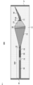
- FIG. 1A and 1B are top views illustrating an optical semiconductor element according to a first embodiment.
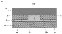
- 1 is a cross-sectional view showing an optical semiconductor element according to a first embodiment.
- FIG. FIG. 5A is a top view showing an optical semiconductor element according to the first embodiment, and FIGS. 5B and 5C are top views showing optical semiconductor elements according to other modifications of the first embodiment.
- FIG. 11 is a top view showing an optical semiconductor element according to a second embodiment.
- FIG. 11 is a cross-sectional view showing an optical semiconductor element according to a second embodiment.
- FIG. 8A and 8B are top views showing an optical semiconductor element according to a first modification of the second embodiment.
- 9A and 9B are top views showing an optical semiconductor element according to a second modification of the second embodiment.
- FIG. 10A is a top view showing an optical semiconductor element according to the second embodiment
- FIGS. 10B, 10C, and 10D are top views showing an optical semiconductor element according to a third modification of the second embodiment.
- FIG. 13 is a top view showing an optical semiconductor element according to a fourth modification of the second embodiment.
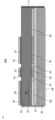
- FIG. 11 is a top view showing an optical semiconductor element according to a third embodiment.
- FIG. 11 is a cross-sectional view showing an optical semiconductor element according to a third embodiment.
- optical semiconductor device according to each embodiment will be described with reference to the drawings.
- the same or corresponding components will be given the same reference numerals, and repeated description may be omitted.
- FIG. 1A and 1B are top views showing optical semiconductor elements 500 and 500a according to embodiment 1.
- the scale of the light propagation direction of the waveguide and the scale of the direction perpendicular to the light propagation direction are compressed to the light propagation direction.
- the optical semiconductor device 500 includes a first waveguide 10, a transparent tapered waveguide 12, a second waveguide 11, and a lateral cladding region 13.
- a first waveguide 10 having a waveguide width W1 a tapered waveguide (hereinafter referred to as a transparent tapered waveguide 12) having a waveguide width W1 at one end on the first waveguide 10 side, a waveguide width W2 at the other end, and a waveguide length L1 in the light propagation direction, which is transparent at the wavelength of the propagating light (hereinafter referred to as the wavelength used), i.e., does not absorb the propagating light
- a second waveguide 11 having a waveguide width W3 are connected in order from the left side of FIG. 1A, i.e., along the light propagation direction.
- the second waveguide 11 is also transparent at the wavelength used.
- the second waveguide 11 and the transparent tapered waveguide 12 can be said to be transparent waveguides at the wavelength used.
- the transparent waveguide is used because it is transparent at the focusing position where the light intensity in the waveguide increases, i.e., the rear part of the transparent tapered waveguide 12 and the second waveguide 11, and therefore it is possible to suppress the occurrence of degradation of the signal light due to gain saturation caused by excessive photon density.
- the mode conversion element i.e., the transparent tapered waveguide 12, which converts the laser light in the first waveguide 10, which has low circularity and is difficult to couple to an optical fiber, into the laser light in the second waveguide 11, which has high circularity and has an improved coupling rate to the optical fiber, while suppressing degradation of the signal light.
- the tapered shape of the transparent tapered waveguide 12 has a relationship of waveguide width W1>waveguide width W2. That is, the transparent tapered waveguide 12 has a shape in which the waveguide width decreases along the light propagation direction from the waveguide width W1 at one end to the waveguide width W2 at the other end.
- the ratio L1/W1 of the waveguide length L1 of the transparent tapered waveguide 12 to the waveguide width W1 at one end of the transparent tapered waveguide 12, i.e., the first waveguide 10 side is 10 or less.
- the mode conversion element i.e., the transparent tapered waveguide 12, which converts the laser light in the first waveguide 10, which has low circularity and is difficult to couple to an optical fiber, into the laser light in the second waveguide 11, which has high circularity and an improved coupling rate to an optical fiber.
- the lateral cladding region 13 is provided in the area other than where the first waveguide 10, the transparent tapered waveguide 12, and the second waveguide 11 are formed.
- the tapered shape of the transparent tapered waveguide 12 is trapezoidal when viewed from above.
- FIG 1B is a top view of an optical semiconductor element 500a in which the waveguide, which is a component of the optical semiconductor element 500 shown in Figure 1A, is used as a gain waveguide. That is, the optical semiconductor element 500a has a first gain waveguide 80, a second gain waveguide 81, a gain tapered waveguide 82, and a lateral cladding region 13.
- the transparent tapered waveguide 12 and the gain tapered waveguide 82 may be collectively referred to simply as a tapered waveguide.
- the optical semiconductor element 500a shown in Figure 1B has the effect of amplifying the intensity of the propagating light, thereby enabling the optical semiconductor element to have a high output.
- the use of the gain tapered waveguide 82 makes it possible to increase the optical intensity within the gain tapered waveguide 82 and the output optical intensity in the gain second waveguide 81 under optical intensity conditions where nonlinear phenomena such as gain saturation, which is likely to occur under high optical intensity and is a cause of optical signal degradation, only cause minor signal degradation.
- Fig. 2 is a cross-sectional view showing an optical semiconductor element 500 according to the first embodiment, showing a cross section taken along line A-A in Fig. 1A.
- the optical semiconductor element 500 is made up of a lower cladding layer 21 and a transparent waveguide core layer 22 formed on a semiconductor substrate 20, and includes a transparent waveguide mesa portion 22a having a convex cross section, lateral cladding layers 23 formed on both side surfaces of the transparent waveguide mesa portion 22a, and an upper cladding layer 24 formed on the upper surface of the transparent waveguide mesa portion 22a and the upper surface of the lateral cladding layer 23.
- a lower cladding layer 21 and a transparent waveguide core layer 22 are sequentially laminated on a semiconductor substrate 20 by epitaxial crystal growth or the like.
- An etching mask having a desired shape is formed by photolithography and etching, and the lateral cladding layer 23 is etched away by dry etching or the like until the entire transparent waveguide core layer 22 and the middle of the lower cladding layer 21 are reached, forming a transparent waveguide mesa portion 22a having a convex shape.
- the lateral cladding layer 23 is grown by buried crystal growth so as to bury both side surfaces of the transparent waveguide mesa portion 22a.
- an upper cladding layer 24 is laminated by epitaxial crystal growth or the like, thereby obtaining the cross-sectional structure shown in FIG. 2.
- the material constituting the transparent waveguide core layer 22 is selected so that the refractive index of the transparent waveguide core layer 22 is higher than the refractive index of each of the lower cladding layer 21, the lateral cladding layer 23, and the upper cladding layer 24.
- examples of such materials include a material in which the semiconductor substrate 20, the lower cladding layer 21, the lateral cladding layer 23, and the upper cladding layer 24 are each made of InP, and the transparent waveguide core layer 22 is made of InGaAsP or InAlGaAs, which is a composition transparent to light of the wavelength used.
- Each of these layers can be epitaxially grown on the semiconductor substrate using known crystal growth techniques.
- Crosses other than the cross section along line A-A in FIG. 1A have the same cross-sectional structure, except that the waveguide width of the transparent waveguide core layer 22 is different.
- a suitable thickness for the upper cladding layer 24 is, for example, 2.0 ⁇ m, and a suitable thickness for the transparent waveguide core layer 22 is, for example, 0.4 ⁇ m.
- the light intensity distribution of the propagating light when fundamental mode light is incident from the first waveguide 10 side is calculated using a commercially available waveguide simulator, and the results are shown in FIG. 3.
- the light intensity is displayed in shades, with darker shades indicating greater light intensity.
- the fundamental mode light incident from one end of the first waveguide 10 enters the transparent tapered waveguide 12 from the other end of the first waveguide 10 and propagates while narrowing the waveguide width.
- the propagating light at the position of line D-D in Figure 3 is very similar to the propagating light in the first waveguide 10. As the propagating light propagates through the transparent tapered waveguide 12, the fundamental mode light is converted to higher mode light, and the shape of the light intensity of the entire propagating light becomes more complex due to interference between the fundamental mode light and the higher mode light.
- the propagating light at the position of line E-E in Figure 3 is no longer at its maximum light intensity in the center of the optical semiconductor element 500 due to interference between guided mode lights of different orders, and exhibits a light intensity shape split into two peaks.
- the phases of the guided mode lights of different orders become aligned, and the light is imaged as a single-peaked light intensity shape having a smaller beam size than the propagating light in the first waveguide 10.
- the propagating light in the first waveguide 10 can be coupled to the second waveguide 11 with low loss. That is, it can be said that the transparent tapered waveguide 12 constituting the optical semiconductor device 500 according to the first embodiment operates as a one-output, one-input MMI (MultiMode Interferometer) capable of mode size conversion.
- MMI MultiMode Interferometer
- the transparent tapered waveguide 12 is significantly lengthened, the fundamental mode light propagates adiabatically in an optical sense, so that conversion to higher-order mode light does not occur, and the intensity distribution of the propagating light remains single-peaked, and does not become the intensity distribution of the propagating light as shown in Figure 3.
- the loss in the optical intensity of the guided light moving from the first waveguide 10 to the second waveguide 11 is a low value of 0.06 dB.
- the element structure of the optical semiconductor element 500 according to the first embodiment it is possible to provide an optical semiconductor element that converts guided light having a large horizontal spot size on the semiconductor substrate 20 and a guided mode shape with low circularity into a guided mode shape with high circularity that is easy to couple to an optical fiber.
- the transparent tapered waveguide 12 has a tapered shape in which the fundamental mode light incident from the other end of the first waveguide 10 propagates to excite higher-order mode light in the transparent tapered waveguide 12, and there is an imaging position where the intensity of the propagating light is imaged at one point due to interference between the fundamental mode light and the higher-order mode light in the transparent tapered waveguide 12, and the transparent tapered waveguide 12 and the second waveguide 11 are connected at this imaging position, so that it is possible to provide an optical semiconductor element that converts guided light having a large horizontal spot size and low circularity into a highly circular guided mode shape that is easy to couple to an optical fiber.
- the above-mentioned imaging position is preferably the position where the light incident from the first waveguide 10 is first imaged when propagating.
- the transparent tapered waveguide 12 and the second waveguide 11 being connected at the imaging position means that the two need only be connected within a range of ⁇ 5 times the optical wavelength, which is a range in which good light-gathering performance is maintained with the imaging position as the center.
- the feature of the device structure of the optical semiconductor device 500 according to the first embodiment is that there is an imaging position where the intensity of the propagating light is imaged at one point due to interference between the fundamental mode light and higher mode light in the transparent tapered waveguide 12, and the transparent tapered waveguide 12 and the second waveguide 11 are connected at this imaging position.
- This configuration can be realized, for example, by using the above-mentioned waveguide simulator to repeat calculations while changing the parameters, such as the waveguide width W1 of the first waveguide 10, the waveguide width W2 on the second waveguide 11 side of the transparent tapered waveguide 12, the waveguide length L1 of the transparent tapered waveguide 12, and the waveguide width W3 of the second waveguide 11.
- ⁇ Modification of the First Embodiment> 4 shows the results of calculating the light intensity distribution of the propagating light when fundamental mode light is incident from the first waveguide 10 side in an optical semiconductor device according to a modified example of the first embodiment, using a commercially available waveguide simulator.
- the light incidence situation is the same as in FIG. 3.
- the light intensity shape of the propagating light at line G-G in Figure 4 is similar to the fundamental mode of the first waveguide 10, as is the light intensity shape of the propagating light at line D-D in Figure 3.
- the light intensity shapes at line H-H and line I-I are qualitatively the same as the light intensity shapes at line E-E and line F-F in Figure 3, respectively, that is, a bimodal shape and a shape imaged at one point in the center of the waveguide.
- the light intensity shape becomes bimodal again at line J-J, and a second image shape is formed at line K-K.
- Figure 4 shows the element structure in which this imaged light is coupled to a second waveguide 11 with a waveguide width that matches the light intensity shape.
- the size of the imaged light at the position of line I-I and the size of the imaged light at the position of line K-K are smaller at the position of line K-K, and the beam size reduction rate at the position of line I-I is inferior.
- the closer the imaging position is to the tip of the tapered shape the closer the intervals between the positions where the imaging positions occur repeatedly, so when coupling to the second waveguide 11, which has a uniform waveguide width, a problem occurs in that the coupling rate becomes more sensitive to variations in element structure.
- the earlier the imaging position appears as in Figure 3 the greater the tolerance of optical coupling to variations in element structure, making it more suitable as an optical semiconductor element.
- FIG. 5A is an enlarged view of the top view of optical semiconductor element 500 according to embodiment 1 shown in Fig. 1A, showing the vicinity of the connection portion between transparent tapered waveguide 12 and second waveguide 11.
- the element structures of optical semiconductor element 510a shown in Fig. 5B and optical semiconductor element 510b shown in Fig. 5C are modifications obtained by modifying the element structure of optical semiconductor element 500 shown in Fig. 5A.
- a connecting transparent tapered waveguide 14 is provided between the transparent tapered waveguide 12 and the second waveguide 11 to connect them.
- the connecting transparent tapered waveguide 14 has a waveguide width W4 at the connection portion with the transparent tapered waveguide 12, and is set to a waveguide width equal to or smaller than the waveguide width W2 of the transparent tapered waveguide 12.
- the waveguide width of the connecting transparent tapered waveguide 14 is set to the same waveguide width as the waveguide width W3 of the second waveguide 11.
- the connecting transparent tapered waveguide 14 has a waveguide length L2 in the light propagation direction.
- the structure of providing a tapered waveguide at the connection between the MMI and the input/output waveguide is desirable because it has the effect of mitigating the phenomenon in which loss during connection changes sensitively to variations in element structure and reducing the reflectance of backlight generated at the junction interface.
- the waveguide length L2 in the light propagation direction of the connecting transparent tapered waveguide 14 there is no particular upper limit to the waveguide length L2 in the light propagation direction of the connecting transparent tapered waveguide 14 as long as reconversion to a higher mode does not occur within the connecting transparent tapered waveguide 14, but it is desirable to make it shorter in terms of miniaturization of the element.
- the waveguide length L2 is set to 10 times or less the wavelength used in order to miniaturize the optical semiconductor element, the effect of improving the tolerance for element structure variations and reducing the return light reflectance can be obtained.
- the transparent tapered waveguide 12 has a trapezoidal shape when viewed from above.
- both sides of the waveguide are not linear but are curved and symmetrical with respect to the center of the optical semiconductor element, as long as the waveguide width is tapered so that it decreases monotonically from the first waveguide 10 side along the light propagation direction, it is possible to obtain an optical semiconductor element that is small, has low loss, and can be converted into a highly circular waveguide mode shape that is easy to couple to an optical fiber, just like in the case of a linear tapered shape.
- the optical semiconductor element according to the first embodiment has a configuration in which an imaging position exists where the intensity of the propagating light is imaged at one point due to interference between the fundamental mode light and higher-order mode light in the tapered waveguide, and the transparent tapered waveguide and the second waveguide are connected at this imaging position, thereby providing an optical semiconductor element that can convert guided light having a guided mode shape with a large spot size in the horizontal direction of the semiconductor substrate and low circularity, into a guided mode shape with high circularity that can be easily coupled to an optical fiber.
- a gain waveguide section 100 is provided so as to be connected to a first waveguide 10, as shown in Fig. 6.
- Fig. 6 is a top view of optical semiconductor device 550, similar to those shown in Figs. 1A and 1B.
- the optical semiconductor element 550 includes, from the incident direction of the signal light, a gain waveguide entrance section 16, a gain tapered waveguide 15, a first waveguide 10, a transparent tapered waveguide 12, and a second waveguide 11.
- the gain waveguide entrance section 16 and the gain tapered waveguide 15 form a gain waveguide section 100.
- a low-reflection coating film 17 is provided on the output end face of the optical semiconductor element 550, and a low-reflection coating film 18 is provided on the input end face.
- the first waveguide 10, the second waveguide 11, and the transparent tapered waveguide 12 have the same element structure as shown in FIG. 1A, that is, the optical semiconductor element 500 according to the first embodiment.
- the gain waveguide entrance section 16 and the gain tapered waveguide 15 are connected in this order from the direction of incidence of the signal light.
- the gain tapered waveguide 15 is connected to the first waveguide 10 at the end opposite the gain waveguide entrance section 16.
- the optical semiconductor element 550 When signal light enters the optical semiconductor element 550 from the gain waveguide entrance portion 16 side and exits from the second waveguide 11 side, the optical intensity of the signal light is amplified in the gain waveguide portion 100.
- a low-reflection coating film 17 on the exit end face of the optical semiconductor element 550 and a low-reflection coating film 18 on the entrance end face it is possible to prevent behavior such as wavelength ripple in the gain spectrum caused by interference of reflected light from both end faces, and therefore the optical semiconductor element 550 can operate as an optical amplifier with reduced wavelength dependency.
- Fig. 7 is a cross-sectional view of an optical semiconductor device 550 according to the second embodiment taken along the line CC in Fig. 6.
- a gain waveguide core layer 25 is laminated on a semiconductor substrate 20 and a lower cladding layer 21 which are common to the device structure of the first embodiment shown in Fig. 2.
- the entire gain waveguide core layer 25 and a part of the lower cladding layer 21 are removed by etching, and the lateral cladding layer 23 is recrystallized.
- an upper cladding layer 24 is laminated to form the cross-sectional structure shown in Fig. 7.
- the etching and the recrystallization of the lateral cladding layer 23 can be performed in the same manner as in the case of forming the device structure of the first embodiment shown in Fig. 2.
- a material is selected so that the refractive index of the gain waveguide core layer 25 is higher than the refractive indexes of the lower cladding layer 21, the lateral cladding layer 23, and the upper cladding layer 24.
- the gain waveguide core layer 25 has an optical gain when the device is operated.
- the semiconductor substrate 20, the lower cladding layer 21, the lateral cladding layer 23, and the upper cladding layer 24 are each made of InP, and the gain waveguide core layer 25 is made of a multiple quantum well layer of InGaAsP or InAlGaAs, which has a composition that has an optical gain for light of a wavelength used when a forward current is injected.
- the semiconductor substrate 20, the lower cladding layer 21, the lateral cladding layer 23, and the upper cladding layer 24 are each made of InP
- the gain waveguide core layer 25 is made of a multiple quantum well layer of InGaAsP or InAlGaAs, which has a composition that has an optical gain for light of a wavelength used when a forward current is injected.
- Each of these layers can be epitaxially grown on the semiconductor substrate using a known crystal growth technique.
- n-type doped n-InP is used for the semiconductor substrate 20 and lower cladding layer 21
- p-type doped p-InP is used for the upper cladding layer 24, while the gain waveguide core layer 25 is intentionally set to be undoped.
- the lateral cladding layer 23 is made of known semi-insulating Fe-doped InP used for current confinement, or known InP with a pn junction that is made highly resistive by creating a reverse bias state at the interface between the p-InP and n-InP.
- a lower electrode 30 is provided on the back surface of the semiconductor substrate 20, and a contact layer 31 and an upper electrode 32 are provided on the upper cladding layer 24.
- An example of the thickness of each layer is 0.5 ⁇ m for the lower cladding layer 21, 0.2 ⁇ m for the gain waveguide core layer 25, and 2.0 ⁇ m for the upper cladding layer 24.
- the specifications of the gain waveguide core layer 25 and the transparent waveguide core layer 22 so that the mode size in the thickness direction of the semiconductor substrate 20 does not diverge between the transparent waveguide and the gain waveguide at the interface with the first waveguide 10.
- the optical semiconductor element 550 according to the second embodiment has the above-described element structure, which allows the current injected from the upper electrode 32 to efficiently reach the gain waveguide core layer 25, thereby generating optical gain for light of the wavelength used.
- the transparent tapered waveguide 12 is adjusted so that the fundamental mode light at the connection on the first waveguide 10 side is coupled to the second waveguide 11 with low loss. Therefore, in order to couple the fundamental mode signal light incident on the gain waveguide section 100 to the second waveguide 11 with as low a loss as possible, it is necessary that the optical intensity of the fundamental mode light among the signal lights amplified at the connection between the gain tapered waveguide 15 and the first waveguide 10 is dominant compared to the optical intensity of the higher mode light that can be excited in the gain tapered waveguide 15.
- the shape of the gain tapered waveguide 15 needs to be elongated with a taper angle equal to or less than the upper limit for adiabatically guiding the light.
- the waveguide width W1 on the first waveguide 10 side is 10 ⁇ m
- the waveguide length L3 of the gain tapered waveguide 15 is 400 ⁇ m or more.
- the upper limit taper angle for adiabatically guiding a wave varies depending on the structure of the gain tapered waveguide 15, i.e., the thickness of the gain waveguide core layer 25 and the refractive index difference with the cladding layer.
- W1 it becomes possible to use a gain tapered waveguide 15 with a shorter waveguide length and a larger taper angle.
- the waveguide width of the gain tapered waveguide 15 can be made wider than that of a semiconductor optical amplifier using a known constant-width waveguide, and as a result, the photon density in the waveguide during optical amplification is reduced, suppressing the gain saturation phenomenon, and thus enabling the total output light from the gain tapered waveguide 15 to be increased.
- FIG. 8A and 8B are top views of an optical semiconductor device 560 and an optical semiconductor device 560a according to the first modification of the second embodiment.
- the optical semiconductor device 560 shown in FIG. 8A includes, from the incident direction of the signal light, an oblique gain waveguide 43, a curved gain waveguide 42, a gain waveguide entrance portion 16, a gain tapered waveguide 15, a first waveguide 10, a transparent tapered waveguide 12, a second waveguide 11, a curved waveguide 40, an oblique waveguide 41, and a lateral cladding region 13.
- a low-reflection coating film 17 is provided on the output side end face of the optical semiconductor device 560, and a low-reflection coating film 18 is provided on the incident side end face.
- the oblique gain waveguide 43, the curved gain waveguide 42, the gain waveguide entrance portion 16, and the gain tapered waveguide 15 constitute a gain waveguide section 101 with oblique incidence.
- the element structure of the optical semiconductor element 560 shown in Fig. 8A has a configuration in which the signal light emitted from the second waveguide 11 is guided to the emission side end face provided with the low reflection coating film 17 via the curved waveguide 40 and the oblique waveguide 41 in the element structure of the optical semiconductor element 550 according to the second embodiment shown in Fig. 6.
- the oblique waveguide 41 is inclined with respect to the emission side end face by an angle of inclination ⁇ 1 compared to the case where the waveguide is perpendicular to the emission side end face.
- An example of the inclination angle ⁇ 1 is 7 degrees.
- a curved gain waveguide 42 and an oblique gain waveguide 43 are provided for the gain waveguide entrance portion 16 to form a gain waveguide portion 101 with oblique incidence, and the light is guided to the entrance end face provided with the low-reflection coating film 18.
- the oblique gain waveguide 43 is inclined by an inclination angle ⁇ 2 compared to when the waveguide is perpendicular to the entrance end face.
- An example of the inclination angle ⁇ 2 is 7 degrees.
- a spot-size conversion waveguide 44 having a tapered shape is provided instead of the diagonal waveguide 41 in FIG. 8A.
- a spot-size conversion gain waveguide 45 having a tapered shape is provided instead of the diagonal gain waveguide 43 in FIG. 8A, thereby forming a gain waveguide with spot-size conversion 102.
- FIGS. 9A and 9B are top views of an optical semiconductor element 570 and an optical semiconductor element 570a according to Modification 2 of Embodiment 2.
- the optical semiconductor element 570 shown in Fig. 9A has an element structure in which the curved gain waveguide 42 and the angled gain waveguide 43 are replaced with a curved waveguide 40 and an angled waveguide 41, which are transparent waveguides.
- the optical semiconductor element 570a shown in FIG. 9B has an element structure in which the diagonal waveguide 41 is replaced with a spot-size conversion waveguide 44. Even with this element structure, as in the case of the element structure shown in FIG. 8A, it is possible to reduce the coupling loss with the optical fiber when inputting and outputting signal light using the optical fiber, thereby realizing an optical amplifier with a large gain.
- Fig. 10A is an enlarged view showing the vicinity of first waveguide 10 in the element structure of optical semiconductor element 550 according to embodiment 2 shown in Fig. 6.
- Figs. 10B, 10C, and 10D are top views showing optical semiconductor elements 580a, 580b, and 580c, respectively, which are modification 3 of embodiment 2.
- the waveguide core layer in a partial region of the first waveguide 10 that contacts the gain taper waveguide 15 is a gain waveguide core layer 25.
- the element structure is such that the interface between the gain waveguide core layer 25 and the transparent waveguide core layer 22 is inclined with respect to the light propagation direction of the waveguide.
- ⁇ Fourth Modification of Second Embodiment> 11 is a top view of an optical semiconductor device 590 according to the fourth modification of the second embodiment, in which, in the device structure shown in FIG. 9A , a part of the side of the gain waveguide entrance portion 16 not in contact with the gain taper type waveguide 15 is made into a transparent waveguide core layer 22, and the interface between the gain waveguide core layer 25 and the transparent waveguide core layer 22 is inclined with respect to the light propagation direction of the waveguide.
- back-reflection that occurs at the interface between the gain waveguide core layer 25 and the transparent waveguide core layer 22 is reduced compared to the element structure shown in FIG. 9A, making it possible to configure an ideal optical amplifier. Since an oblique interface can be provided at the gain waveguide entrance portion 16 not only for the element structure shown in FIG. 9A but also for the element structure shown in FIG. 9B, it becomes possible to configure an ideal optical amplifier with a similar reduction in back-reflection.
- the optical semiconductor element according to the second embodiment has an effect that, by appropriately connecting a gain waveguide to the element structure of the optical semiconductor element according to the first embodiment, it is possible to convert the amplified signal light into a waveguide mode shape with high circularity that is small, has low loss, and is easy to couple to an optical fiber.
- ⁇ Third embodiment> 12 is a top view of an optical semiconductor device 600 according to the third embodiment.
- the optical semiconductor device 600 according to the third embodiment includes, from the incident direction of the signal light, a laser light source section 50, a laser light modulator connection section 51, an optical modulator section 52, an optical modulator gain waveguide connection section 53, a gain waveguide entrance section 16, a gain tapered waveguide 15, a first waveguide 10, a transparent tapered waveguide 12, a connecting transparent tapered waveguide 14, a second waveguide 11, a bent waveguide 40, a spot size conversion waveguide 44, and a lateral cladding region 13.
- the laser light source section 50, the laser light modulator connection section 51, the optical modulator section 52, and the optical modulator gain waveguide connection section 53 constitute a modulated signal light generating section 200.
- a high-reflection coating film 19 is provided on the emission end face of the optical semiconductor element 600, and a low-reflection coating film 18 is provided on the incidence end face.
- the optical semiconductor device 600 according to the third embodiment is characterized in that, as compared to the optical semiconductor device 550 according to the second embodiment, a modulated signal light generating section 200 is provided so as to be connected to the gain waveguide entrance section 16 as shown in FIG. 12.
- the modulated signal light generating section 200 is made up of a laser light source section 50 which is a distributed feedback semiconductor laser (DFB laser) and an optical modulator section 52 which is an electroabsorption optical modulator, which are connected via a laser optical modulator connection section 51 which is a transparent waveguide, and the optical modulator section 52 is connected to the gain waveguide entrance section 16 via an optical modulator gain waveguide connection section 53 which is a transparent waveguide.
- DFB laser distributed feedback semiconductor laser
- an optical modulator section 52 which is an electroabsorption optical modulator
- the modulated signal light generating unit 200 may have other configurations, such as a directly modulated semiconductor laser, a semiconductor laser with a Mach-Zehnder optical modulator, or a semiconductor laser with a microring optical modulator.
- FIG. 13 is a cross-sectional view of the optical semiconductor element 600 according to embodiment 3 shown in FIG. 12, taken along a cross section (non-planar) along the center of the straight and curved waveguides, parallel to the substrate thickness direction.
- the cross section from the laser light source unit 50 to the curved waveguide 40 is perpendicular to the substrate end face, and the cross section from the curved waveguide 40 to the spot size conversion waveguide 44 is inclined relative to the substrate end face.
- the layers through which the signal light is guided are, in the direction in which the signal light is incident, a laser active layer 60, a transparent waveguide core layer 61, an optical modulator active layer 62, a transparent waveguide core layer 63, a gain waveguide core layer 25, and a transparent waveguide core layer 22.
- the semiconductor substrate 20, the lower cladding layer 21, and the upper cladding layer 24 have the same element structure as the optical semiconductor element 550 according to the second embodiment.
- a lower electrode 30 is provided on the back surface of the semiconductor substrate 20.
- a contact layer 35 and an upper electrode 36 are provided for injecting current into the laser light source unit 50.
- a laser active layer 60 that is not intentionally doped with a dopant is laminated on the lower cladding layer 21, and a diffraction grating 70 is provided above and adjacent to the laser active layer 60 to output light of a wavelength used as a distributed feedback semiconductor laser.
- the diffraction grating 70 may have a structure in which known phase shift points with different diffraction grating intervals are provided inside, which is known to have the effect of stabilizing the single mode oscillation of the semiconductor laser.
- a high-reflection coating film 19 is provided on the incident end surface on the laser light source unit 50 side to increase the output light to the gain tapered waveguide 15 side.
- the transparent waveguide core layer 61 and the transparent waveguide core layer 63 are formed together with the same composition and thickness as the transparent waveguide core layer 22.
- the optical modulator active layer 62 is composed of a multiple quantum well layer adjusted so that the oscillation wavelength of the laser light source unit 50 is in the wavelength region near the absorption edge, and the quantum confined Stark effect occurs when a reverse bias is applied, increasing the optical absorption coefficient in the wavelength region near the absorption edge.
- a contact layer 33 and an upper electrode 34 are provided to apply a reverse bias to the optical modulator active layer 62.
- the laser light modulator connection part 51 and the light modulator gain waveguide connection part 53 are set to the necessary waveguide length so that the upper electrode 36, the upper electrode 34, and the upper electrode 32 do not cause low resistance in their mutual electrical isolation.
- One example of such a waveguide length is when the laser light modulator connection part 51 and the light modulator gain waveguide connection part 53 each have a waveguide length of 50 ⁇ m.
- an independent constant forward voltage is applied between the upper electrode 36 and the upper electrode 32 to drive the laser light source section 50 and the gain waveguide section 100.
- An appropriate reverse bias voltage and a modulated electrical signal in which a high-frequency voltage signal encoded for optical communication is superimposed are applied to the upper electrode 34.
- the optical absorption coefficient of the optical modulator section 52 changes in response to the applied modulated electrical signal, generating modulated signal light.
- the modulated signal light enters the gain waveguide section 100, where the fundamental mode is dominant and the light intensity is amplified, reaching the first waveguide 10. Then, as the modulated signal light propagates through the transparent tapered waveguide 12, it is converted into a highly circular guided mode shape that is small, has low loss, and is easy to couple to an optical fiber, reaching the second waveguide 11, and finally exiting from the spot size conversion waveguide 44.
- a modulated signal light generating unit is further provided, which has the effect of increasing the output of the modulated optical signal by the optical amplifier and enabling the output light to be shaped into a good beam.
Landscapes
- Physics & Mathematics (AREA)
- Optics & Photonics (AREA)
- Nonlinear Science (AREA)
- General Physics & Mathematics (AREA)
- Electromagnetism (AREA)
- Condensed Matter Physics & Semiconductors (AREA)
- Engineering & Computer Science (AREA)
- Plasma & Fusion (AREA)
- Microelectronics & Electronic Packaging (AREA)
- Optical Integrated Circuits (AREA)
- Semiconductor Lasers (AREA)
- Optical Modulation, Optical Deflection, Nonlinear Optics, Optical Demodulation, Optical Logic Elements (AREA)
- Lasers (AREA)
Priority Applications (4)
| Application Number | Priority Date | Filing Date | Title |
|---|---|---|---|
| CN202380097777.1A CN121175890A (zh) | 2023-05-15 | 2023-05-15 | 光半导体元件 |
| PCT/JP2023/018127 WO2024236697A1 (ja) | 2023-05-15 | 2023-05-15 | 光半導体素子 |
| JP2023566997A JP7442754B1 (ja) | 2023-05-15 | 2023-05-15 | 光半導体素子 |
| JP2024004283A JP7446553B1 (ja) | 2023-05-15 | 2024-01-16 | 光半導体素子 |
Applications Claiming Priority (1)
| Application Number | Priority Date | Filing Date | Title |
|---|---|---|---|
| PCT/JP2023/018127 WO2024236697A1 (ja) | 2023-05-15 | 2023-05-15 | 光半導体素子 |
Publications (1)
| Publication Number | Publication Date |
|---|---|
| WO2024236697A1 true WO2024236697A1 (ja) | 2024-11-21 |
Family
ID=90096850
Family Applications (1)
| Application Number | Title | Priority Date | Filing Date |
|---|---|---|---|
| PCT/JP2023/018127 Ceased WO2024236697A1 (ja) | 2023-05-15 | 2023-05-15 | 光半導体素子 |
Country Status (3)
| Country | Link |
|---|---|
| JP (2) | JP7442754B1 (https=) |
| CN (1) | CN121175890A (https=) |
| WO (1) | WO2024236697A1 (https=) |
Citations (5)
| Publication number | Priority date | Publication date | Assignee | Title |
|---|---|---|---|---|
| JP2010003950A (ja) * | 2008-06-23 | 2010-01-07 | Nec Corp | 光半導体装置 |
| JP2012113267A (ja) * | 2010-11-29 | 2012-06-14 | Canon Inc | 光走査装置 |
| JP2014154680A (ja) * | 2013-02-07 | 2014-08-25 | Furukawa Electric Co Ltd:The | 半導体レーザ装置 |
| US20200366061A1 (en) * | 2018-02-05 | 2020-11-19 | Zhejiang University | Tunable semiconductor laser based on half-wave coupled partial reflectors |
| JP2021158268A (ja) * | 2020-03-27 | 2021-10-07 | 株式会社デンソー | 半導体発光素子 |
Family Cites Families (7)
| Publication number | Priority date | Publication date | Assignee | Title |
|---|---|---|---|---|
| US6614585B1 (en) | 1999-05-06 | 2003-09-02 | Trumpf Photonics Inc. | Phase conjugating structure for mode matching in super luminescent diode cavities |
| EP1507321B1 (en) | 2003-08-11 | 2006-10-25 | Lumera Laser GmbH | Solid state laser pumped by a laser diode with a convergent beam |
| JP5268733B2 (ja) * | 2009-03-25 | 2013-08-21 | 富士通株式会社 | 光導波素子とその製造方法、半導体素子、レーザモジュール及び光伝送システム |
| CN106921441A (zh) * | 2017-03-13 | 2017-07-04 | 南京邮电大学 | 一种可实现无差异混频的相干光接收机 |
| JP6412969B2 (ja) * | 2017-03-14 | 2018-10-24 | 沖電気工業株式会社 | 光導波路素子 |
| CN211126441U (zh) * | 2020-03-05 | 2020-07-28 | 度亘激光技术(苏州)有限公司 | 一种激光器 |
| CN111308829A (zh) | 2020-04-10 | 2020-06-19 | 上海大学 | 一种PbS/SiO2共掺纳米集成锥形光纤放大器及其制备方法 |
-
2023
- 2023-05-15 WO PCT/JP2023/018127 patent/WO2024236697A1/ja not_active Ceased
- 2023-05-15 JP JP2023566997A patent/JP7442754B1/ja active Active
- 2023-05-15 CN CN202380097777.1A patent/CN121175890A/zh active Pending
-
2024
- 2024-01-16 JP JP2024004283A patent/JP7446553B1/ja active Active
Patent Citations (5)
| Publication number | Priority date | Publication date | Assignee | Title |
|---|---|---|---|---|
| JP2010003950A (ja) * | 2008-06-23 | 2010-01-07 | Nec Corp | 光半導体装置 |
| JP2012113267A (ja) * | 2010-11-29 | 2012-06-14 | Canon Inc | 光走査装置 |
| JP2014154680A (ja) * | 2013-02-07 | 2014-08-25 | Furukawa Electric Co Ltd:The | 半導体レーザ装置 |
| US20200366061A1 (en) * | 2018-02-05 | 2020-11-19 | Zhejiang University | Tunable semiconductor laser based on half-wave coupled partial reflectors |
| JP2021158268A (ja) * | 2020-03-27 | 2021-10-07 | 株式会社デンソー | 半導体発光素子 |
Also Published As
| Publication number | Publication date |
|---|---|
| JP7446553B1 (ja) | 2024-03-08 |
| JPWO2024236697A1 (https=) | 2024-11-21 |
| JP2024164794A (ja) | 2024-11-27 |
| JP7442754B1 (ja) | 2024-03-04 |
| CN121175890A (zh) | 2025-12-19 |
Similar Documents
| Publication | Publication Date | Title |
|---|---|---|
| US6768758B1 (en) | Semiconductor laser, semiconductor optical amplifier, and production method thereof | |
| US9088132B2 (en) | Semiconductor optical element, integrated semiconductor optical element, and semiconductor optical element module | |
| US7262435B2 (en) | Single-transverse-mode laser diode with multi-mode waveguide region and manufacturing method of the same | |
| JP4942429B2 (ja) | 半導体波長可変レーザ | |
| JP3991615B2 (ja) | 半導体光アンプおよび半導体レーザ | |
| JP4906185B2 (ja) | 光半導体素子及び光半導体素子の変調方法 | |
| US5155737A (en) | Semiconductor wavelength conversion device | |
| JP2016072608A (ja) | 半導体レーザおよびこれを備える光集積光源 | |
| JP2937148B2 (ja) | 半導体集積型偏波モード変換器 | |
| JP2018060974A (ja) | 半導体光集積素子 | |
| JP7442754B1 (ja) | 光半導体素子 | |
| JP2950302B2 (ja) | 半導体レーザ | |
| WO2025013161A1 (ja) | 半導体光集積素子、半導体光集積素子の製造方法、半導体光装置および半導体光装置の制御方法 | |
| JP6761391B2 (ja) | 半導体光集積素子 | |
| JP7541271B2 (ja) | 半導体レーザ及び光送信器 | |
| JP3006553B2 (ja) | 半導体集積型偏波モード変換器 | |
| JP4033822B2 (ja) | Dbr型波長可変光源 | |
| JPS60260017A (ja) | 光変調素子 | |
| JP2760276B2 (ja) | 選択成長導波型光制御素子 | |
| JP2005117045A (ja) | 利得固定半導体光増幅器 | |
| JP7560005B1 (ja) | 光半導体装置 | |
| US12259561B2 (en) | Spot-size converter | |
| JP3196958B2 (ja) | 変調器集積半導体レーザ | |
| WO2026022890A1 (ja) | 光半導体素子 | |
| JPS61107781A (ja) | 単一軸モ−ド半導体レ−ザ装置 |
Legal Events
| Date | Code | Title | Description |
|---|---|---|---|
| WWE | Wipo information: entry into national phase |
Ref document number: 2023566997 Country of ref document: JP |
|
| 121 | Ep: the epo has been informed by wipo that ep was designated in this application |
Ref document number: 23937441 Country of ref document: EP Kind code of ref document: A1 |
|
| NENP | Non-entry into the national phase |
Ref country code: DE |