WO2024232348A1 - ノイズ検出装置、ノイズ抑圧装置、ノイズ検出方法およびプログラム - Google Patents
ノイズ検出装置、ノイズ抑圧装置、ノイズ検出方法およびプログラム Download PDFInfo
- Publication number
- WO2024232348A1 WO2024232348A1 PCT/JP2024/016923 JP2024016923W WO2024232348A1 WO 2024232348 A1 WO2024232348 A1 WO 2024232348A1 JP 2024016923 W JP2024016923 W JP 2024016923W WO 2024232348 A1 WO2024232348 A1 WO 2024232348A1
- Authority
- WO
- WIPO (PCT)
- Prior art keywords
- phase
- noise
- carrier
- frequency
- correction
- Prior art date
- Legal status (The legal status is an assumption and is not a legal conclusion. Google has not performed a legal analysis and makes no representation as to the accuracy of the status listed.)
- Ceased
Links
Images






Classifications
-
- H—ELECTRICITY
- H04—ELECTRIC COMMUNICATION TECHNIQUE
- H04B—TRANSMISSION
- H04B1/00—Details of transmission systems, not covered by a single one of groups H04B3/00 - H04B13/00; Details of transmission systems not characterised by the medium used for transmission
- H04B1/06—Receivers
- H04B1/10—Means associated with receiver for limiting or suppressing noise or interference
-
- H—ELECTRICITY
- H04—ELECTRIC COMMUNICATION TECHNIQUE
- H04B—TRANSMISSION
- H04B17/00—Monitoring; Testing
- H04B17/20—Monitoring; Testing of receivers
-
- H—ELECTRICITY
- H04—ELECTRIC COMMUNICATION TECHNIQUE
- H04L—TRANSMISSION OF DIGITAL INFORMATION, e.g. TELEGRAPHIC COMMUNICATION
- H04L27/00—Modulated-carrier systems
- H04L27/01—Equalisers
-
- H—ELECTRICITY
- H04—ELECTRIC COMMUNICATION TECHNIQUE
- H04L—TRANSMISSION OF DIGITAL INFORMATION, e.g. TELEGRAPHIC COMMUNICATION
- H04L27/00—Modulated-carrier systems
- H04L27/02—Amplitude-modulated carrier systems, e.g. using on-off keying; Single sideband or vestigial sideband modulation
-
- H—ELECTRICITY
- H04—ELECTRIC COMMUNICATION TECHNIQUE
- H04L—TRANSMISSION OF DIGITAL INFORMATION, e.g. TELEGRAPHIC COMMUNICATION
- H04L27/00—Modulated-carrier systems
- H04L27/26—Systems using multi-frequency codes
- H04L27/2601—Multicarrier modulation systems
- H04L27/2647—Arrangements specific to the receiver only
- H04L27/2649—Demodulators
- H04L27/265—Fourier transform demodulators, e.g. fast Fourier transform [FFT] or discrete Fourier transform [DFT] demodulators
Definitions
- This disclosure relates to a noise detection device for detecting noise contained in an input signal.
- Patent Document 1 discloses a noise suppression device that uses symmetry in the frequency spectrum (amplitude spectrum) of the amplitude of an AM signal to suppress components that are not symmetric in the amplitude spectrum as noise, in order to suppress noise with a small amount of calculation.
- the present disclosure provides a noise detection device and the like that can detect noise even when the noise exists at a symmetrical position in the amplitude spectrum.
- the noise detection device is a noise detection device for detecting noise contained in an input signal including a carrier wave and a modulated signal, and includes a DFT execution unit that performs a discrete Fourier transform on the input signal and outputs a transformation result, a carrier wave detection unit that detects a carrier frequency bin that is a frequency bin that includes the carrier wave component in the transformation result, a frequency correction unit that performs a correction to reduce the difference between the center frequency of the carrier frequency bin and the frequency of the carrier wave, a phase calculation unit that calculates the phase of each signal component in the post-correction transformation result that is the transformation result output after the correction, a phase inversion unit that inverts the phase of each signal component based on the center frequency of the carrier frequency bin in the post-correction transformation result, and an asymmetric component detection unit that detects, as noise, signal components whose phase is asymmetric with respect to the carrier frequency bin in the post-correction transformation result, based on the phase before and after inversion of each signal component.
- the noise suppression device includes the noise detection device described above, a suppression coefficient calculation unit that calculates a suppression coefficient for suppressing the amplitude of the signal component detected as the noise, and an IDFT execution unit that performs an inverse discrete Fourier transform on the corrected transformation result multiplied by the suppression coefficient to output an output signal.
- the noise detection device is a noise detection device for detecting noise contained in an input signal including a carrier wave and a modulated signal, and includes a DFT execution unit that performs a discrete Fourier transform on the input signal and outputs a transformation result, a carrier detection unit that detects a carrier frequency bin that is a frequency bin that includes the carrier wave component in the transformation result, a phase calculation unit that calculates the phase of each signal component in the transformation result, a phase inversion unit that inverts the phase of each signal component based on the center frequency of the carrier frequency bin in the transformation result, and an asymmetric component detection unit that detects, as noise, signal components whose phases are asymmetric with respect to the center frequency of the carrier frequency bin in the transformation result based on the phases of each signal component before and after inversion.
- the noise detection method is a noise detection method executed by a noise detection device for detecting noise contained in an input signal including a carrier wave and a modulated signal, and includes a DFT execution step of performing a discrete Fourier transform on the input signal to output a transformation result, a carrier detection step of detecting a carrier frequency bin that is a frequency bin that includes the carrier wave component in the transformation result, a frequency correction step of performing a correction to reduce the difference between the center frequency of the carrier frequency bin and the frequency of the carrier wave, a phase calculation step of calculating the phase of each signal component in the post-correction transformation result that is the transformation result output after the correction, a phase inversion step of inverting the phase of each signal component with reference to the center frequency of the carrier frequency bin in the post-correction transformation result, and an asymmetric component detection step of detecting, as noise, a signal component whose phase is asymmetric with reference to the carrier frequency bin in the post-correction transformation result, based on the phase before and after inversion
- the program disclosed herein is a program for causing a computer to execute the above-mentioned noise detection method.
- a noise detection device can detect noise even when the noise is present at a symmetrical position in the amplitude spectrum.
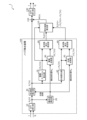
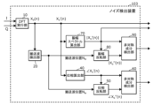
- FIG. 1 is a block diagram showing an example of a noise suppression device according to a first embodiment
- 4 is a diagram for explaining the operation of a carrier wave detection unit
- FIG. 11 is a diagram for explaining the operation of a frequency correction unit.
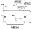
- FIG. 10 is a diagram illustrating a schematic diagram of a correction for reducing the difference between the center frequency of a carrier frequency bin and the frequency of a carrier wave.
- FIG. 13 is a diagram showing how the phase of the modulated component becomes symmetrical with respect to the center frequency of the carrier frequency bin as a result of the correction.
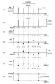
- FIG. 4 is a diagram for explaining the operation of the noise suppression device according to the first embodiment
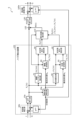
- FIG. 11 is a block diagram showing an example of a noise suppression device according to a second embodiment.
- FIG. 11 is a block diagram showing an example of a noise suppression device according to a third embodiment.
- FIG. 13 is a block diagram showing an example of a noise suppression device according to a fourth embodiment.
- FIG. 13 is a block diagram showing an example of a noise suppression device according to a fifth embodiment.
- FIG. 13 is a block diagram showing an example of a noise detection device according to another embodiment.
- 13 is a flowchart illustrating an example of a noise detection method according to another embodiment.
- FIG. 1 is a block diagram showing an example of a noise suppression device 1 according to embodiment 1.
- the noise suppression device 1 is a device for suppressing noise contained in an input signal (e.g., an I/Q signal) that includes a carrier wave and a modulated signal.
- an input signal e.g., an I/Q signal
- the input signal is a broadcast wave.
- the output signal output from the noise suppression device 1 (the input signal with noise suppressed) is subjected to a demodulation process.
- the noise suppression device 1 includes a noise detection device 100, a suppression coefficient calculation unit 110, a multiplication unit 120, and an IDFT execution unit 130.
- the noise detection device 100 is a device for detecting noise contained in an input signal.
- the noise detection device 100 detects noise contained in the input signal, and the noise suppression device 1 is able to suppress the noise contained in the input signal.
- the noise detection device 100 includes a DFT execution unit 10, a carrier detection unit 20, a frequency correction unit 30, a phase calculation unit 40, a phase inversion unit 50, an asymmetric component detection unit 60, an amplitude spectrum calculation unit 70, an amplitude inversion unit 80, and an asymmetric component detection unit 90.
- the noise detection device 100 is a computer including a processor (microprocessor) and a memory.
- the memory is a ROM (Read Only Memory) and a RAM (Random Access Memory), and can store a program executed by the processor.
- the DFT execution unit 10, the carrier detection unit 20, the frequency correction unit 30, the phase calculation unit 40, the phase inversion unit 50, the asymmetric component detection unit 60, the amplitude spectrum calculation unit 70, the amplitude inversion unit 80, and the asymmetric component detection unit 90 are realized by a processor that executes a program stored in the memory.
- the suppression coefficient calculation unit 110, the multiplication unit 120, and the IDFT execution unit 130 are also realized by a processor that executes a program stored in a memory.
- the DFT execution unit 10, the carrier detection unit 20, the frequency correction unit 30, the phase calculation unit 40, the phase inversion unit 50, the asymmetric component detection unit 60, the amplitude spectrum calculation unit 70, the amplitude inversion unit 80, and the asymmetric component detection unit 90 which are the functional units of the noise detection device 100, and the suppression coefficient calculation unit 110, the multiplication unit 120, and the IDFT execution unit 130 may be realized by a single computer.
- the DFT execution unit 10 performs a discrete Fourier transform (DFT) on the input signal and outputs the transformation result (frequency spectrum).
- DFT discrete Fourier transform
- the carrier wave detection unit 20 detects carrier frequency bins, which are frequency bins that contain carrier wave components in the conversion result of the DFT execution unit 10. The operation of the carrier wave detection unit 20 will be explained using FIG. 2.
- FIG. 2 is a diagram for explaining the operation of the carrier wave detection unit 20.
- FIG. 2 shows the amplitude spectrum of the input signal.
- the carrier wave detection unit 20 determines the component with the highest amplitude in the amplitude spectrum near the receiving frequency as the carrier wave.
- the carrier wave detection unit 20 may determine a signal that has been determined to be a carrier wave continuously as a carrier wave. For example, even if high-amplitude noise appears locally near the receiving frequency, the noise is not determined to be a carrier wave, and the signal that has been determined to be a carrier wave as a carrier wave can be determined to be a carrier wave.
- the carrier wave detection unit 20 detects a frequency bin that includes a carrier wave component as a carrier wave frequency bin.
- the carrier wave detection unit 20 outputs the position (frequency) of the detected carrier wave to the phase inversion unit 50 and the amplitude inversion unit 80.
- the carrier wave detection unit 20 detects the phase of the carrier wave in the conversion result of the DFT execution unit 10. Specifically, the carrier wave detection unit 20 detects the phase of the carrier wave for each frame. When the phase of the carrier wave changes for each frame, the carrier wave detection unit 20 outputs a phase error, which is the amount of change in the phase of the carrier wave between frames, to the frequency correction unit 30.
- the frequency correction unit 30 performs correction to reduce the difference between the center frequency of the carrier frequency bin and the carrier frequency. The operation of the frequency correction unit 30 will be explained using FIG. 3.
- FIG. 3 is a diagram for explaining the operation of the frequency correction unit 30.
- FIG. 3 shows the complex representation of the components of the carrier frequency bin.
- the frequency correction unit 30 performs the above correction based on the phase of the carrier detected by the carrier detection unit 20.
- the frequency correction unit 30 performs the above correction by performing a convolution operation based on the phase of the carrier on the conversion result of the DFT execution unit 10.
- the phase rotates for each frame, i.e., a phase error occurs.
- the phase error is output from the carrier detection unit 20 to the frequency correction unit 30.
- the frequency correction unit 30 performs a convolution operation to correct the phase of the carrier in the current frame in order to reduce the phase error (for example, to zero).
- the phase error is ⁇
- a convolution operation is performed to correct the phase of the carrier in the current frame by 0 to ⁇ . This makes it possible to reduce the difference between the center frequency of the carrier frequency bin and the frequency of the carrier.
- the carrier frequency bin deviates from the actual frequency of the carrier, when the components of the carrier frequency bin are expressed in complex numbers, the components rotate for each frame (a phase error occurs). Therefore, by detecting the phase of the carrier and performing a correction so that no phase error occurs, it is possible to reduce the difference between the center frequency of the carrier frequency bin and the frequency of the carrier. For example, a convolution operation can be performed in the frequency domain to perform a correction so that no phase error occurs.
- the frequency correction unit 30 may also perform a convolution operation to correct the phase of the carrier wave in the current frame in order to reduce (e.g., set to 0) the deviation angle of the carrier wave phase ( ⁇ 0 shown in FIG. 3 ). This allows the deviation angle to be fixed at, for example, 0°.
- Figure 4 is a diagram that shows a schematic of the correction that reduces the difference between the center frequency of the carrier frequency bin and the carrier frequency.
- Figure 4 shows the amplitude spectrum of the input signal.
- Figure 5 shows how the phase of the modulated component becomes symmetrical with respect to the center frequency of the carrier frequency bin as a result of the correction.
- Figure 5 also shows the phase spectrum of the input signal.
- the carrier frequency bin in the result of the DFT will deviate from the actual frequency of the carrier.
- the frequency indicated by "2" is the center frequency of the carrier frequency bin, it can be seen that the carrier frequency bin deviates from the actual frequency of the carrier.
- the components of the modulated signal are not symmetrical in amplitude with respect to the carrier frequency bin. Therefore, it is not possible to compare the amplitudes before and after the inversion of the amplitude spectrum by the amplitude spectrum calculation unit 70, the amplitude inversion unit 80, and the asymmetric component detection unit 90 described later. Also, as shown in the upper part of FIG.
- the phase rotates as shown in FIG. 3 due to the effect of the frequency difference, so the components of the modulated signal are not symmetrical in phase with respect to the carrier frequency bin. Therefore, it is not possible to compare the phases before and after the inversion of the phase spectrum by the phase calculation unit 40, the phase inversion unit 50, and the asymmetric component detection unit 60 described later.
- the amplitude is a scalar quantity, as described in Patent Document 1, it is possible to compare the amplitudes by allowing a shift in the frequency direction.
- phase is an angle component, and the phase of each frequency bin will have a different value due to the difference between the frequency of each frequency bin and the frequency of the signal. For this reason, it is not possible to compare phases while allowing for shifts in the frequency direction, as is the case with amplitude.
- the components of the modulated signal become symmetrical in amplitude with respect to the carrier frequency bin, as shown in the lower part of Figure 4.
- the amount of phase rotation due to the frequency difference also becomes symmetrical, and the components of the modulated signal become symmetrical in phase with respect to the carrier frequency bin.
- the frequency correction unit 30 outputs the corrected conversion result, which is the conversion result of the DFT execution unit 10 after correction, to the phase calculation unit 40 and the amplitude spectrum calculation unit 70.
- the frequency correction unit 30 also outputs the corrected conversion result to outside the noise detection device 100 (e.g., to the multiplication unit 120).
- the phase calculation unit 40 calculates the phase of each signal component in the corrected conversion result, which is the conversion result of the DFT execution unit 10 and is output after correction.
- Each signal component may include a noise component in addition to a carrier wave component and a modulated signal component.
- the phase calculation unit 40 outputs the calculated phase of each signal component to the phase inversion unit 50 and the asymmetric component detection unit 60.
- the phase inversion unit 50 inverts the phase of each signal component based on the center frequency of the carrier frequency bin in the post-correction conversion result.
- the phase inversion unit 50 outputs the inverted phase of each signal component to the asymmetric component detection unit 60.
- the asymmetric component detection unit 60 detects, as noise, signal components whose phases are asymmetric with respect to the carrier frequency bin in the post-correction conversion result, based on the phase of each signal component before inversion (specifically, the phase output from the phase calculation unit 40) and the phase after inversion (specifically, the phase output from the phase inversion unit 50).
- the amplitude spectrum calculation unit 70 calculates the amplitude of each signal component in the post-correction conversion result.
- the amplitude spectrum calculation unit 70 outputs the calculated amplitude of each signal component to the amplitude inversion unit 80 and the asymmetric component detection unit 90.
- the amplitude inversion unit 80 inverts the amplitude of each signal component based on the center frequency of the carrier frequency bin in the post-correction conversion result.
- the amplitude inversion unit 80 outputs the inverted amplitude of each signal component to the asymmetric component detection unit 90.
- the asymmetric component detection unit 90 detects, as noise, signal components whose amplitudes are asymmetric with respect to the carrier frequency bin in the post-correction conversion result, based on the amplitude of each signal component before inversion (specifically, the amplitude output from the amplitude spectrum calculation unit 70) and the amplitude after inversion (specifically, the amplitude output from the amplitude inversion unit 80).
- the suppression coefficient calculation unit 110 calculates a suppression coefficient for suppressing the amplitude of the signal component detected as noise.
- the multiplication unit 120 multiplies the corrected conversion result by the suppression coefficient. This suppresses noise.
- the IDFT execution unit 130 performs an inverse discrete Fourier transform (IDFT) on the corrected transformation result multiplied by the suppression coefficient, and outputs an output signal.
- IDFT inverse discrete Fourier transform
- FIG. 6 is a diagram for explaining the operation of the noise suppression device 1 according to the first embodiment.
- FIG. 6(a) is a diagram showing the output (
- FIG. 6(b) is a diagram showing the output (
- FIG. 6(c) is a diagram showing the output (D 0 (n)) of the asymmetric component detection unit 90.
- FIG. 6(d) is a diagram showing the output ( ⁇ X 0 '(n)) of the phase calculation unit 40.
- FIG. 6(e) is a diagram showing the output ( ⁇ X 0 ''(n)) of the phase inversion unit 50.
- FIG. 6(f) is a diagram showing the output (E 0 (n)) of the asymmetric component detection unit 60.
- FIG. 6(g) is a diagram showing the output (W(n)) of
- the correction by the frequency correction unit 30 causes the amplitude of the broadcast wave component (component of the modulated signal) to be symmetrical between the frequencies N M -N S and N M +N S with respect to the carrier frequency bin N M.
- noise may also have symmetrical amplitude with respect to the carrier frequency bin.
- the noise amplitude is symmetrical between the frequencies N M -N B and N M +N B with respect to the carrier frequency bin N M.
- the amplitude inversion unit 80 inverts the amplitude of each signal component based on the center frequency of the carrier frequency bin in the amplitude spectrum.
- the asymmetric component detection unit 90 detects signal components whose amplitudes are asymmetric by calculating the difference between the amplitude spectrum before and after inversion. As shown in (a) and (b) of FIG. 6, the amplitudes of the signal components are symmetric with respect to the carrier frequency bin, so the difference is 0, as shown in (c) of FIG. 6. For this reason, if the amplitude of noise is symmetric with respect to the carrier frequency bin, the asymmetric component detection unit 90 cannot detect the noise.
- the asymmetric component detection unit 90 can detect the noise. Details of the method for detecting noise when the noise amplitude is not symmetrical with respect to the carrier frequency bin (i.e., details of the operation of the amplitude spectrum calculation unit 70, the amplitude inversion unit 80, and the asymmetric component detection unit 90) are described in Patent Document 1, so a description thereof will be omitted.
- the correction by frequency correction unit 30 causes the phase of the broadcast wave component (modulated signal component) to be symmetrical between the frequency N M -N S and the frequency N M +N S with respect to the carrier frequency bin N M. Note that since noise is a signal that is not synchronized with the carrier wave, even if the amplitude is symmetrical, the phase is asymmetrical.
- phase inversion unit 50 As shown in FIG. 6(e), it can be seen that the phase of each signal component is inverted by the phase inversion unit 50 with reference to the center frequency of the carrier frequency bin in the phase spectrum.
- the asymmetric component detection unit 60 detects signal components whose phase is asymmetric by calculating the difference between the phase spectrum before and after inversion. As shown in (d) and (e) of FIG. 6, the components of the modulated signal are symmetric in phase with respect to the carrier frequency bin, so the difference is zero, as shown in (f) of FIG. 6. On the other hand, the noise is asymmetric in phase with respect to the carrier frequency bin, so the absolute value of the difference is greater than zero, as shown in (f) of FIG. 6. For this reason, even if the amplitude of the noise is symmetric with respect to the carrier frequency bin, the asymmetric component detection unit 60 can detect the noise.
- the suppression coefficient calculation unit 110 calculates a suppression coefficient for suppressing the amplitude of the signal component detected as noise for each position (frequency) of the detected noise. There are no particular limitations on the method of calculating the suppression coefficient, but a suppression coefficient is calculated that reduces (e.g., makes zero) the amplitude of the signal component detected as noise in the amplitude spectrum. The calculated suppression coefficient is then multiplied by the corrected conversion result to suppress the noise contained in the input signal.
- the components of the modulated signal are ideally symmetric in amplitude and phase with respect to the carrier frequency bin.
- noise may have symmetric amplitude with respect to the carrier frequency bin, but because noise is a signal that is not synchronized with the carrier wave, even if the amplitude is symmetric, the phase is asymmetric. Therefore, the noise detection device 100 inverts the phase of each signal component, which may also include noise, with respect to the center frequency of the carrier frequency bin in the transformation result, and compares the phase of each signal component before and after inversion, thereby making it possible to detect signal components whose phase is asymmetric with respect to the carrier frequency bin as noise. Therefore, even if noise is present in a symmetric position in the amplitude spectrum, it can be detected.
- the carrier frequency bin in the DFT transformation result will deviate from the actual frequency of the carrier.
- the components of the modulated signal will not be symmetric in phase with respect to the carrier frequency bin.
- the components of the modulated signal will also be asymmetric in phase with respect to the carrier frequency bin, and there is a risk that the components of the modulated signal will be erroneously detected as noise. Therefore, by performing a correction to reduce the difference between the center frequency of the carrier frequency bin and the frequency of the carrier, it is possible to reduce the deviation between the carrier frequency bin and the actual frequency of the carrier. This makes it possible to prevent the components of the modulated signal from becoming asymmetric in phase with respect to the carrier frequency bin, and to prevent the components of the modulated signal from being erroneously detected as noise.
- the noise suppression device 1 can detect noise contained in the input signal and output an output signal in which the noise has been suppressed. For example, even when it is difficult to detect the carrier wave, such as when there is a large noise near the frequency of the carrier wave or when sudden large pulse noise is applied, it is possible to suppress the signal equivalent to the conventional method by suppressing only the portion where the amplitude difference is detected, and it is possible to prevent a decrease in the suppression function.
- FIG. 7 is a block diagram showing an example of a noise suppression device 2 according to embodiment 2.
- Noise suppression device 2 differs from noise suppression device 1 according to embodiment 1 in that it further includes a frequency inverse correction unit 140. Below, the differences from embodiment 1 will be mainly described, and the same points will not be described.
- the frequency inverse correction unit 140 performs an inverse correction to return the difference between the center frequency of the carrier frequency bin in the post-correction conversion result multiplied by the suppression coefficient and the carrier frequency to the state before correction.
- the frequency inverse correction unit 140 can perform the inverse correction by obtaining the phase error used in the correction by the frequency correction unit 30 from the carrier detection unit 20.
- the phase may rotate depending on the carrier position. For example, when performing FFT by shifting by 1/2 frame, if the carrier position is shifted by 1 bin from the center, the data of the next frame starts from a position rotated by 1/2 x 360°, so the phase appears to rotate by 180° for each frame. In this case, when the phase of the carrier frequency bin is set to 0°, the phase is inverted for each frame when combining after IDFT, and therefore the signals cannot be combined correctly. Even in such a case, the signals can be combined correctly by performing inverse correction by the frequency inverse correction unit 140.
- FIG. 8 is a block diagram showing an example of a noise suppression device 3 according to embodiment 3.
- Noise suppression device 3 differs from noise suppression device 1 according to embodiment 1 in that it has noise detection device 101 instead of noise detection device 100.
- Noise detection device 101 also differs from noise detection device 100 according to embodiment 1 in that it has frequency correction unit 30a instead of frequency correction unit 30, and an input signal is input to frequency correction unit 30a without passing through DFT execution unit 10.
- the frequency correction unit 30a includes a phase adjustment unit 31 and a DFT execution unit 32.
- the phase adjustment unit 31 adjusts the phase of the input signal so that the phase of the carrier wave is reduced, and the DFT execution unit 32 executes DFT on the input signal whose phase has been adjusted so that the phase of the carrier wave is reduced, and outputs the conversion result.
- the frequency correction unit 30a (DFT execution unit 32) outputs the corrected conversion result, which is the conversion result of the corrected DFT execution unit 32, to the phase calculation unit 40 and the amplitude spectrum calculation unit 70.
- the adjustment of the phase of the input signal by the phase adjustment unit 31 will be explained again with reference to FIG. 3.
- the phase adjustment unit 31 adjusts the phase of the input signal based on the phase of the carrier detected by the carrier detection unit 20.
- the phase rotates for each frame, as shown in FIG. 3, i.e., a phase error occurs.
- the phase error is output from the carrier detection unit 20 to the phase adjustment unit 31. Therefore, in order to reduce the phase error (for example, to zero), the phase adjustment unit 31 adjusts the phase of the input signal so as to correct the phase of the carrier in the current frame.
- the frequency correction unit 30a can perform a correction to reduce the difference between the center frequency of the carrier frequency bin and the carrier frequency.
- frequency inverse correction may be performed in the time domain.
- FIG. 9 is a block diagram showing an example of a noise suppression device 4 according to embodiment 4.
- Noise suppression device 4 differs from noise suppression device 1 according to embodiment 1 in that it includes noise detection device 102 instead of noise detection device 100.
- Noise detection device 102 also differs from noise detection device 100 according to embodiment 1 in that it includes frequency correction unit 30b, DFT execution unit 10a, and carrier detection unit 20a instead of frequency correction unit 30, DFT execution unit 10, and carrier detection unit 20, and an input signal is input to frequency correction unit 30b, and the corrected input signal is input to DFT execution unit 10a.
- the frequency correction unit 30b performs a correction to reduce the difference between the center frequency of the carrier frequency bin and the carrier frequency by adjusting the phase of the input signal so that the phase of the carrier is reduced.
- the DFT execution unit 10a performs a discrete Fourier transform on the input signal whose phase has been adjusted by the above correction.
- the carrier detection unit 20a detects the carrier frequency bin in the post-correction transformation result, and detects the phase of the carrier after subtracting the amount of phase adjustment by the above correction.
- the amount of phase adjustment of the input signal in the time domain in frequency correction unit 30b is information obtained by calculation within noise detection device 102, so by performing processing in frequency correction unit 30b before processing in DFT execution unit 10a and subtracting the amount of phase adjustment in frequency correction unit 30b when detecting the phase (specifically, the phase error) of carrier detection unit 20a, it is possible to share the DFT execution unit used to detect carrier waves and the DFT execution unit used to detect noise.
- noise detection device 102 of embodiment 4 there is no need to provide DFT execution unit 10 and DFT execution unit 32 separately, as in noise detection device 101 of embodiment 3, and processing costs can be reduced.
- FIG. 10 is a block diagram showing an example of a noise suppression device 5 according to embodiment 5.
- Noise suppression device 5 differs from noise suppression device 4 according to embodiment 4 in that it further includes a frequency inverse correction unit 140a. Below, the differences from embodiment 4 will be mainly described, and the same points will not be described.
- the frequency inverse correction unit 140a performs inverse correction to return the difference between the center frequency of the carrier frequency bin in the post-correction conversion result multiplied by the suppression coefficient and the carrier frequency to the state before correction.
- the frequency inverse correction unit 140a can perform inverse correction by obtaining the phase error used in the correction by the frequency correction unit 30b from the carrier detection unit 20a.
- the effect achieved by providing the frequency inverse correction unit 140a is the same as the effect achieved by providing the frequency inverse correction unit 140.
- the noise detection device includes a frequency correction unit, but as shown in FIG. 11, the noise detection device does not need to include a frequency correction unit.
- FIG. 11 is a block diagram showing an example of a noise detection device 103 according to another embodiment.
- the noise detection device 103 differs from the noise detection device 100 according to the first embodiment in that it does not include a frequency correction unit 30.
- the phase calculation unit 40 calculates the phase of each signal component in the conversion result
- the phase inversion unit 50 inverts the phase of each signal component with reference to the center frequency of the carrier frequency bin in the conversion result
- the asymmetric component detection unit 60 detects, as noise, signal components whose phases are asymmetric with reference to the center frequency of the carrier frequency bin in the conversion result based on the phase before and after inversion of each signal component.
- the phase calculation unit 40, the phase inversion unit 50, and the asymmetric component detection unit 60 performed processing using the corrected conversion result, but in the third embodiment, since the noise detection device 103 does not include a frequency correction unit 30, the phase calculation unit 40, the phase inversion unit 50, and the asymmetric component detection unit 60 perform processing using the conversion result that has not been corrected by the frequency correction unit 30.
- the noise detection device 103 does not include a frequency correction unit 30
- the phase calculation unit 40, the phase inversion unit 50, and the asymmetric component detection unit 60 perform processing using the conversion result that has not been corrected by the frequency correction unit 30.
- Other points are the same as those in the first embodiment, so a description thereof will be omitted.
- the noise detection devices according to embodiments 1 to 5 may be replaced with the noise detection device 103.
- the noise detection device includes an amplitude spectrum calculation unit 70, an amplitude inversion unit 80, and an asymmetric component detection unit 90, but the noise detection device does not have to include an amplitude spectrum calculation unit 70, an amplitude inversion unit 80, and an asymmetric component detection unit 90.
- the present disclosure can be realized not only as a noise detection device or a noise suppression device, but also as a noise detection method including steps (processing) performed by components that make up a noise detection device.
- FIG. 12 is a flowchart showing an example of a noise detection method according to another embodiment.
- the noise detection method is a noise detection method executed by a noise detection device for detecting noise contained in an input signal including a carrier wave and a modulated signal, and includes, as shown in FIG. 12, a DFT execution step (step S11) for performing a discrete Fourier transform on the input signal and outputting the transformation result, a carrier detection step (step S12) for detecting a carrier frequency bin, which is a frequency bin including a carrier wave component in the transformation result, a frequency correction step (step S13) for performing a correction to reduce the difference between the center frequency of the carrier frequency bin and the frequency of the carrier wave, a phase calculation step (step S14) for calculating the phase of each signal component in the post-correction transformation result, which is the transformation result output after the correction, a phase inversion step (step S15) for inverting the phase of each signal component with reference to the center frequency of the carrier frequency bin in the post-correction transformation result, and an asymmetric component detection step (step S16) for detecting, as noise, a signal
- the present disclosure can be realized as a program for causing a computer (processor) to execute the steps included in the noise detection method.
- the present disclosure can be realized as a non-transitory computer-readable recording medium, such as a CD-ROM, on which the program is recorded.
- each step is performed by running the program using hardware resources such as a computer's CPU, memory, and input/output circuits.
- hardware resources such as a computer's CPU, memory, and input/output circuits.
- each step is performed by the CPU obtaining data from memory or input/output circuits, etc., performing calculations, and outputting the results of the calculations to memory or input/output circuits, etc.
- each component included in the noise detection device may be configured with dedicated hardware, or may be realized by executing a software program suitable for each component.
- Each component may be realized by a program execution unit such as a CPU or processor reading and executing a software program recorded on a recording medium such as a hard disk or semiconductor memory.
- LSI is an integrated circuit. These may be individually integrated into a single chip, or may be integrated into a single chip that includes some or all of the functions. Furthermore, the integrated circuit is not limited to an LSI, and may be realized using a dedicated circuit or a general-purpose processor.
- An FPGA Field Programmable Gate Array
- reconfigurable processor that can reconfigure the connections and settings of circuit cells inside the LSI, may also be used.
- each component included in the noise detection device may be integrated into an integrated circuit using that technology.
- this disclosure also includes forms obtained by applying various modifications to the embodiments that a person skilled in the art may conceive, and forms realized by arbitrarily combining the components and functions of each embodiment within the scope that does not deviate from the spirit of this disclosure.
- a noise detection device for detecting noise contained in an input signal including a carrier wave and a modulated signal, the noise detection device comprising: a DFT execution unit that performs a discrete Fourier transform on the input signal and outputs a transformation result; a carrier wave detection unit that detects a carrier wave frequency bin that is a frequency bin that includes the carrier wave component in the transformation result; a frequency correction unit that performs a correction to reduce the difference between the center frequency of the carrier wave frequency bin and the frequency of the carrier wave; a phase calculation unit that calculates the phase of each signal component in the post-correction transformation result that is the transformation result output after the correction; a phase inversion unit that inverts the phase of each signal component with reference to the center frequency of the carrier wave frequency bin in the post-correction transformation result; and an asymmetric component detection unit that detects, as noise, signal components whose phases are asymmetric with reference to the carrier wave frequency bin in the post-correction transformation result, based on the phases of each signal component before and after
- the components of the modulated signal are ideally symmetric in amplitude and phase with respect to the carrier frequency bin.
- noise may have symmetric amplitude with respect to the carrier frequency bin, but because noise is a signal that is not synchronized with the carrier wave, even if the amplitude is symmetric, the phase is asymmetric. Therefore, by inverting the phase of each signal component, which may also include noise, with respect to the center frequency of the carrier frequency bin in the transformation result as a reference, and comparing the phase of each signal component before and after inversion, it is possible to detect signal components whose phase is asymmetric with respect to the carrier frequency bin as noise. Therefore, noise can be detected even if it is present in a symmetric position in the amplitude spectrum.
- the carrier frequency bin in the DFT transformation result will deviate from the actual frequency of the carrier.
- the components of the modulated signal will not be symmetric in phase with respect to the carrier frequency bin.
- the components of the modulated signal will also be asymmetric in phase with respect to the carrier frequency bin, and there is a risk that the components of the modulated signal will be erroneously detected as noise. Therefore, by performing a correction to reduce the difference between the center frequency of the carrier frequency bin and the frequency of the carrier, it is possible to reduce the deviation between the carrier frequency bin and the actual frequency of the carrier. This makes it possible to prevent the components of the modulated signal from becoming asymmetric in phase with respect to the carrier frequency bin, and to prevent the components of the modulated signal from being erroneously detected as noise.
- the carrier frequency bin deviates from the actual frequency of the carrier, when the components of the carrier frequency bin are expressed in complex numbers, the components rotate for each frame (a phase error occurs). Therefore, by detecting the phase of the carrier and performing correction so that no phase error occurs, it is possible to reduce the difference between the center frequency of the carrier frequency bin and the frequency of the carrier.
- the amount of phase adjustment of the input signal in the time domain in the frequency correction unit is information obtained by calculation within the noise detection device, so by performing processing in the frequency correction unit before processing in the DFT execution unit and subtracting the amount of phase adjustment in the frequency correction unit when detecting the phase (specifically, the phase error) in the carrier detection unit, it is possible to share the same DFT execution unit between the DFT execution unit used to detect the carrier wave and the DFT execution unit used to detect noise.
- a noise suppression device comprising a noise detection device according to any one of techniques 1 to 5, a suppression coefficient calculation unit that calculates a suppression coefficient for suppressing the amplitude of the signal component detected as the noise, and an IDFT execution unit that performs an inverse discrete Fourier transform on the corrected transformation result multiplied by the suppression coefficient to output an output signal.
- the noise suppression device described in Technology 6 further includes a frequency inverse correction unit that performs inverse correction to return the difference between the center frequency of the carrier frequency bin in the corrected conversion result multiplied by the suppression coefficient and the frequency of the carrier to the state before the correction was performed.
- the phase may rotate depending on the carrier position. For example, when performing FFT by shifting by 1/2 frame, if the carrier position is shifted by 1 bin from the center, the data of the next frame starts from a position rotated by 1/2 x 360°, so the phase appears to rotate by 180° for each frame. In this case, when the phase of the carrier frequency bin is set to 0°, the phase is inverted for each frame when combining after IDFT, and therefore the combination cannot be performed correctly. Even in such a case, the signals can be combined correctly by performing an inverse correction by the frequency inverse correction section.
- a noise detection device for detecting noise contained in an input signal including a carrier wave and a modulated signal, the noise detection device comprising: a DFT execution unit that performs a discrete Fourier transform on the input signal and outputs a transformation result; a carrier wave detection unit that detects a carrier wave frequency bin that is a frequency bin that includes the carrier wave component in the transformation result; a phase calculation unit that calculates the phase of each signal component in the transformation result; a phase inversion unit that inverts the phase of each signal component with reference to the center frequency of the carrier wave frequency bin in the transformation result; and an asymmetric component detection unit that detects, as noise, signal components whose phases are asymmetric with reference to the center frequency of the carrier wave frequency bin in the transformation result, based on the phases of each signal component before and after inversion.
- the components of the modulated signal are ideally symmetric in amplitude and phase with respect to the carrier frequency bin.
- noise may have symmetric amplitude with respect to the carrier frequency bin, but because noise is a signal that is not synchronized with the carrier wave, even if the amplitude is symmetric, the phase is asymmetric. Therefore, by inverting the phase of each signal component, which may also include noise, with respect to the center frequency of the carrier frequency bin in the transformation result as a reference, and comparing the phase of each signal component before and after inversion, it is possible to detect signal components whose phase is asymmetric with respect to the carrier frequency bin as noise. Therefore, noise can be detected even if it is present in a symmetric position in the amplitude spectrum.
- a noise detection method executed by a noise detection device for detecting noise contained in an input signal including a carrier wave and a modulated signal including: a DFT execution step of performing a discrete Fourier transform on the input signal to output a transformation result; a carrier detection step of detecting a carrier frequency bin that is a frequency bin that includes the carrier wave component in the transformation result; a frequency correction step of performing a correction to reduce the difference between the center frequency of the carrier frequency bin and the frequency of the carrier wave; a phase calculation step of calculating the phase of each signal component in the post-correction transformation result that is the transformation result output after the correction; a phase inversion step of inverting the phase of each signal component with reference to the center frequency of the carrier frequency bin in the post-correction transformation result; and an asymmetric component detection step of detecting, as noise, a signal component whose phase is asymmetric with reference to the carrier frequency bin in the post-correction transformation result, based on the phase before and after inversion of
- This provides a noise detection method that can detect noise even when the noise exists at a symmetrical position in the amplitude spectrum.
- This disclosure can be applied to devices that suppress noise contained in broadcast waves, etc.
- Noise suppression device 10a 1, 2, 3, 4, 5 Noise suppression device 10, 10a, 32 DFT execution unit 20, 20a Carrier detection unit 30, 30a, 30b Frequency correction unit 31 Phase adjustment unit 40 Phase calculation unit 50 Phase inversion unit 60, 90 Asymmetric component detection unit 70 Amplitude spectrum calculation unit 80 Amplitude inversion unit 100, 101, 102, 103 Noise detection device 110 Suppression coefficient calculation unit 120 Multiplication unit 130 IDFT execution unit 140, 140a Frequency inverse correction unit
Landscapes
- Engineering & Computer Science (AREA)
- Computer Networks & Wireless Communication (AREA)
- Signal Processing (AREA)
- Physics & Mathematics (AREA)
- Discrete Mathematics (AREA)
- General Physics & Mathematics (AREA)
- Mathematical Physics (AREA)
- Electromagnetism (AREA)
- Noise Elimination (AREA)
Priority Applications (2)
| Application Number | Priority Date | Filing Date | Title |
|---|---|---|---|
| JP2025519433A JPWO2024232348A1 (https=) | 2023-05-09 | 2024-05-07 | |
| US19/369,937 US20260051913A1 (en) | 2023-05-09 | 2025-10-27 | Noise detection device, noise suppression device, noise detection method, and recording medium |
Applications Claiming Priority (2)
| Application Number | Priority Date | Filing Date | Title |
|---|---|---|---|
| US202363501048P | 2023-05-09 | 2023-05-09 | |
| US63/501,048 | 2023-05-09 |
Related Child Applications (1)
| Application Number | Title | Priority Date | Filing Date |
|---|---|---|---|
| US19/369,937 Continuation US20260051913A1 (en) | 2023-05-09 | 2025-10-27 | Noise detection device, noise suppression device, noise detection method, and recording medium |
Publications (1)
| Publication Number | Publication Date |
|---|---|
| WO2024232348A1 true WO2024232348A1 (ja) | 2024-11-14 |
Family
ID=93429987
Family Applications (1)
| Application Number | Title | Priority Date | Filing Date |
|---|---|---|---|
| PCT/JP2024/016923 Ceased WO2024232348A1 (ja) | 2023-05-09 | 2024-05-07 | ノイズ検出装置、ノイズ抑圧装置、ノイズ検出方法およびプログラム |
Country Status (3)
| Country | Link |
|---|---|
| US (1) | US20260051913A1 (https=) |
| JP (1) | JPWO2024232348A1 (https=) |
| WO (1) | WO2024232348A1 (https=) |
Citations (3)
| Publication number | Priority date | Publication date | Assignee | Title |
|---|---|---|---|---|
| JP2015156577A (ja) * | 2014-02-20 | 2015-08-27 | パイオニア株式会社 | 放送受信装置及びノイズ除去方法 |
| WO2018116943A1 (ja) * | 2016-12-22 | 2018-06-28 | パナソニックIpマネジメント株式会社 | ノイズ抑圧装置、ノイズ抑圧方法、及びこれらを用いた受信装置、受信方法 |
| WO2021229715A1 (ja) * | 2020-05-13 | 2021-11-18 | 三菱電機株式会社 | ノイズ除去装置、アンテナ装置、及びノイズ除去方法 |
-
2024
- 2024-05-07 WO PCT/JP2024/016923 patent/WO2024232348A1/ja not_active Ceased
- 2024-05-07 JP JP2025519433A patent/JPWO2024232348A1/ja active Pending
-
2025
- 2025-10-27 US US19/369,937 patent/US20260051913A1/en active Pending
Patent Citations (3)
| Publication number | Priority date | Publication date | Assignee | Title |
|---|---|---|---|---|
| JP2015156577A (ja) * | 2014-02-20 | 2015-08-27 | パイオニア株式会社 | 放送受信装置及びノイズ除去方法 |
| WO2018116943A1 (ja) * | 2016-12-22 | 2018-06-28 | パナソニックIpマネジメント株式会社 | ノイズ抑圧装置、ノイズ抑圧方法、及びこれらを用いた受信装置、受信方法 |
| WO2021229715A1 (ja) * | 2020-05-13 | 2021-11-18 | 三菱電機株式会社 | ノイズ除去装置、アンテナ装置、及びノイズ除去方法 |
Also Published As
| Publication number | Publication date |
|---|---|
| US20260051913A1 (en) | 2026-02-19 |
| JPWO2024232348A1 (https=) | 2024-11-14 |
Similar Documents
| Publication | Publication Date | Title |
|---|---|---|
| US10205461B2 (en) | Integrated circuit having a clock deskew circuit that includes an injection-locked oscillator | |
| US6366148B1 (en) | Delay locked loop circuit and method for generating internal clock signal | |
| US20120022676A1 (en) | Audio signal processing apparatus, audio coding apparatus, and audio decoding apparatus | |
| US20090180527A1 (en) | Measuring apparatus, measuring method, recording medium, and test apparatus | |
| JP6935425B2 (ja) | ノイズ抑圧装置、ノイズ抑圧方法、及びこれらを用いた受信装置、受信方法 | |
| JP2002290214A (ja) | デューティーサイクル補正回路 | |
| EP3796611B1 (en) | Phase calibration method and device | |
| CA2689812A1 (en) | Rd converter and angle detecting apparatus | |
| US8184762B2 (en) | Digital phase lock loop with multi-phase master clock | |
| JP5337157B2 (ja) | 試験装置、及び試験方法 | |
| US8682182B2 (en) | Blind carrier frequency offset detection for coherent receivers using quadrature amplitude modulation formats | |
| US7948260B1 (en) | Method and apparatus for aligning the phases of digital clock signals | |
| US9143312B2 (en) | Using a single phase error algorithm for coarse and fine signal timing synchronisation | |
| WO2024232348A1 (ja) | ノイズ検出装置、ノイズ抑圧装置、ノイズ検出方法およびプログラム | |
| JP5752072B2 (ja) | 正弦波信号のパラメーターを求める方法及びシステム | |
| US9691372B2 (en) | Noise suppression device, noise suppression method, and non-transitory computer-readable recording medium storing program for noise suppression | |
| JP2008211619A (ja) | 復調特性測定装置、直交復調器、復調特性測定方法、プログラム、記録媒体 | |
| WO2013108590A1 (ja) | 直交変換誤差補正装置 | |
| US11979182B2 (en) | Noise elimination device, antenna device, and noise elimination method | |
| US20230163774A1 (en) | Distortion reduction circuit | |
| US9806722B2 (en) | High frequency delay lock loop systems | |
| JPH02146844A (ja) | 直交位相誤差検出回路 | |
| US11595031B1 (en) | Circuit and method for eliminating spurious signal | |
| JP2013207737A (ja) | 位相検出回路、半導体装置及び位相検出方法 | |
| US11784729B2 (en) | Calibration device, conversion device, calibration method, and non-transitory computer-readable medium having recorded thereon calibration program |
Legal Events
| Date | Code | Title | Description |
|---|---|---|---|
| 121 | Ep: the epo has been informed by wipo that ep was designated in this application |
Ref document number: 24803459 Country of ref document: EP Kind code of ref document: A1 |
|
| ENP | Entry into the national phase |
Ref document number: 2025519433 Country of ref document: JP Kind code of ref document: A |
|
| WWE | Wipo information: entry into national phase |
Ref document number: 2025519433 Country of ref document: JP |
|
| NENP | Non-entry into the national phase |
Ref country code: DE |