WO2024232138A1 - 半導体装置とその製造方法 - Google Patents
半導体装置とその製造方法 Download PDFInfo
- Publication number
- WO2024232138A1 WO2024232138A1 PCT/JP2024/005259 JP2024005259W WO2024232138A1 WO 2024232138 A1 WO2024232138 A1 WO 2024232138A1 JP 2024005259 W JP2024005259 W JP 2024005259W WO 2024232138 A1 WO2024232138 A1 WO 2024232138A1
- Authority
- WO
- WIPO (PCT)
- Prior art keywords
- region
- type
- cathode
- diode
- igbt
- Prior art date
- Legal status (The legal status is an assumption and is not a legal conclusion. Google has not performed a legal analysis and makes no representation as to the accuracy of the status listed.)
- Ceased
Links
Images





Classifications
-
- H—ELECTRICITY
- H10—SEMICONDUCTOR DEVICES; ELECTRIC SOLID-STATE DEVICES NOT OTHERWISE PROVIDED FOR
- H10D—INORGANIC ELECTRIC SEMICONDUCTOR DEVICES
- H10D8/00—Diodes
- H10D8/422—PN diodes having the PN junctions in mesas
-
- H—ELECTRICITY
- H10—SEMICONDUCTOR DEVICES; ELECTRIC SOLID-STATE DEVICES NOT OTHERWISE PROVIDED FOR
- H10D—INORGANIC ELECTRIC SEMICONDUCTOR DEVICES
- H10D84/00—Integrated devices formed in or on semiconductor substrates that comprise only semiconducting layers, e.g. on Si wafers or on GaAs-on-Si wafers
- H10D84/101—Integrated devices comprising main components and built-in components, e.g. IGBT having built-in freewheel diode
- H10D84/161—IGBT having built-in components
-
- H—ELECTRICITY
- H10—SEMICONDUCTOR DEVICES; ELECTRIC SOLID-STATE DEVICES NOT OTHERWISE PROVIDED FOR
- H10D—INORGANIC ELECTRIC SEMICONDUCTOR DEVICES
- H10D12/00—Bipolar devices controlled by the field effect, e.g. insulated-gate bipolar transistors [IGBT]
-
- H—ELECTRICITY
- H10—SEMICONDUCTOR DEVICES; ELECTRIC SOLID-STATE DEVICES NOT OTHERWISE PROVIDED FOR
- H10D—INORGANIC ELECTRIC SEMICONDUCTOR DEVICES
- H10D12/00—Bipolar devices controlled by the field effect, e.g. insulated-gate bipolar transistors [IGBT]
- H10D12/411—Insulated-gate bipolar transistors [IGBT]
- H10D12/441—Vertical IGBTs
- H10D12/461—Vertical IGBTs having non-planar surfaces, e.g. having trenches, recesses or pillars in the surfaces of the emitter, base or collector regions
- H10D12/481—Vertical IGBTs having non-planar surfaces, e.g. having trenches, recesses or pillars in the surfaces of the emitter, base or collector regions having gate structures on slanted surfaces, on vertical surfaces, or in grooves, e.g. trench gate IGBTs
-
- H—ELECTRICITY
- H10—SEMICONDUCTOR DEVICES; ELECTRIC SOLID-STATE DEVICES NOT OTHERWISE PROVIDED FOR
- H10D—INORGANIC ELECTRIC SEMICONDUCTOR DEVICES
- H10D30/00—Field-effect transistors [FET]
- H10D30/01—Manufacture or treatment
- H10D30/021—Manufacture or treatment of FETs having insulated gates [IGFET]
-
- H—ELECTRICITY
- H10—SEMICONDUCTOR DEVICES; ELECTRIC SOLID-STATE DEVICES NOT OTHERWISE PROVIDED FOR
- H10D—INORGANIC ELECTRIC SEMICONDUCTOR DEVICES
- H10D30/00—Field-effect transistors [FET]
- H10D30/60—Insulated-gate field-effect transistors [IGFET]
-
- H—ELECTRICITY
- H10—SEMICONDUCTOR DEVICES; ELECTRIC SOLID-STATE DEVICES NOT OTHERWISE PROVIDED FOR
- H10D—INORGANIC ELECTRIC SEMICONDUCTOR DEVICES
- H10D62/00—Semiconductor bodies, or regions thereof, of devices having potential barriers
- H10D62/10—Shapes, relative sizes or dispositions of the regions of the semiconductor bodies; Shapes of the semiconductor bodies
- H10D62/129—Cathode regions of diodes
-
- H—ELECTRICITY
- H10—SEMICONDUCTOR DEVICES; ELECTRIC SOLID-STATE DEVICES NOT OTHERWISE PROVIDED FOR
- H10D—INORGANIC ELECTRIC SEMICONDUCTOR DEVICES
- H10D62/00—Semiconductor bodies, or regions thereof, of devices having potential barriers
- H10D62/50—Physical imperfections
- H10D62/53—Physical imperfections the imperfections being within the semiconductor body
-
- H—ELECTRICITY
- H10—SEMICONDUCTOR DEVICES; ELECTRIC SOLID-STATE DEVICES NOT OTHERWISE PROVIDED FOR
- H10D—INORGANIC ELECTRIC SEMICONDUCTOR DEVICES
- H10D62/00—Semiconductor bodies, or regions thereof, of devices having potential barriers
- H10D62/60—Impurity distributions or concentrations
-
- H—ELECTRICITY
- H10—SEMICONDUCTOR DEVICES; ELECTRIC SOLID-STATE DEVICES NOT OTHERWISE PROVIDED FOR
- H10D—INORGANIC ELECTRIC SEMICONDUCTOR DEVICES
- H10D64/00—Electrodes of devices having potential barriers
- H10D64/111—Field plates
- H10D64/117—Recessed field plates, e.g. trench field plates or buried field plates
-
- H—ELECTRICITY
- H10—SEMICONDUCTOR DEVICES; ELECTRIC SOLID-STATE DEVICES NOT OTHERWISE PROVIDED FOR
- H10D—INORGANIC ELECTRIC SEMICONDUCTOR DEVICES
- H10D8/00—Diodes
- H10D8/01—Manufacture or treatment
- H10D8/045—Manufacture or treatment of PN junction diodes
-
- H—ELECTRICITY
- H10—SEMICONDUCTOR DEVICES; ELECTRIC SOLID-STATE DEVICES NOT OTHERWISE PROVIDED FOR
- H10D—INORGANIC ELECTRIC SEMICONDUCTOR DEVICES
- H10D84/00—Integrated devices formed in or on semiconductor substrates that comprise only semiconducting layers, e.g. on Si wafers or on GaAs-on-Si wafers
- H10D84/01—Manufacture or treatment
- H10D84/0107—Integrating at least one component covered by H10D12/00 or H10D30/00 with at least one component covered by H10D8/00, H10D10/00 or H10D18/00, e.g. integrating IGFETs with BJTs
- H10D84/0109—Integrating at least one component covered by H10D12/00 or H10D30/00 with at least one component covered by H10D8/00, H10D10/00 or H10D18/00, e.g. integrating IGFETs with BJTs the at least one component covered by H10D12/00 or H10D30/00 being a MOS device
-
- H—ELECTRICITY
- H10—SEMICONDUCTOR DEVICES; ELECTRIC SOLID-STATE DEVICES NOT OTHERWISE PROVIDED FOR
- H10D—INORGANIC ELECTRIC SEMICONDUCTOR DEVICES
- H10D84/00—Integrated devices formed in or on semiconductor substrates that comprise only semiconducting layers, e.g. on Si wafers or on GaAs-on-Si wafers
- H10D84/80—Integrated devices formed in or on semiconductor substrates that comprise only semiconducting layers, e.g. on Si wafers or on GaAs-on-Si wafers characterised by the integration of at least one component covered by groups H10D12/00 or H10D30/00, e.g. integration of IGFETs
- H10D84/811—Combinations of field-effect devices and one or more diodes, capacitors or resistors
-
- H—ELECTRICITY
- H10—SEMICONDUCTOR DEVICES; ELECTRIC SOLID-STATE DEVICES NOT OTHERWISE PROVIDED FOR
- H10D—INORGANIC ELECTRIC SEMICONDUCTOR DEVICES
- H10D64/00—Electrodes of devices having potential barriers
- H10D64/20—Electrodes characterised by their shapes, relative sizes or dispositions
- H10D64/27—Electrodes not carrying the current to be rectified, amplified, oscillated or switched, e.g. gates
- H10D64/311—Gate electrodes for field-effect devices
- H10D64/411—Gate electrodes for field-effect devices for FETs
- H10D64/511—Gate electrodes for field-effect devices for FETs for IGFETs
- H10D64/512—Disposition of the gate electrodes, e.g. buried gates
- H10D64/513—Disposition of the gate electrodes, e.g. buried gates within recesses in the substrate, e.g. trench gates, groove gates or buried gates
Definitions
- the technology disclosed in this specification relates to a semiconductor device and a manufacturing method thereof.
- Patent Document 1 discloses a method for manufacturing a semiconductor device having an insulated gate bipolar transistor and a diode.
- the insulated gate bipolar transistor may be referred to as an IGBT (i.e., an insulated gate bipolar transistor).
- a semiconductor device having an IGBT and a diode may be referred to as an RC-IGBT.
- an n-type cathode region is formed by ion implantation of n-type impurities.
- crystal defects are formed in the cathode region by irradiating the semiconductor substrate with helium ions. By forming crystal defects in the cathode region, snapback can be suppressed when the IGBT is turned on.
- the voltage applied to the diode may change rapidly.
- the recovery current may decay too quickly, causing a surge voltage. If crystal defects exist in the cathode region, the recovery current is more likely to decay, making it easier for a surge voltage to occur.
- the semiconductor device disclosed in this specification includes a semiconductor substrate having an IGBT region and a diode region, an upper electrode in contact with an upper surface of the semiconductor substrate in the IGBT region and the diode region, a lower electrode in contact with a lower surface of the semiconductor substrate in the IGBT region and the diode region, and a gate electrode.
- the semiconductor substrate includes an emitter region, an upper p-type region, a drift region, a field stop region, a collector region, a plurality of cathode regions, and a plurality of surge suppression regions.
- the emitter region is an n-type region in contact with the upper electrode in the IGBT region.
- the upper p-type region is distributed across the IGBT region and the diode region, and is in contact with the upper electrode in the IGBT region and the diode region.
- the drift region is an n-type region disposed below the upper p-type region, distributed across the IGBT region and the diode region, and separated from the emitter region by the upper p-type region.
- the field stop region is disposed below the drift region, has a higher n-type impurity concentration than the drift region, has a mountain-shaped distribution in the n-type impurity concentration distribution along the thickness direction of the semiconductor substrate, and is an n-type region distributed across the IGBT region and the diode region.
- the collector region is disposed in the IGBT region, is disposed below the field stop region, and is a p-type region in contact with the lower electrode.
- the plurality of cathode regions are disposed in the diode region, are disposed below the field stop region, and are n-type regions in contact with the lower electrode.
- the plurality of surge suppression regions are disposed in the diode region, are disposed below the field stop region, and are p-type regions in contact with the lower electrode.
- the gate electrode faces the upper p-type region between the emitter region and the drift region via a gate insulating film. In the diode region, the plurality of cathode regions and the plurality of surge suppression regions are alternately disposed along a specific direction on the lower surface of the semiconductor substrate.
- Each of the cathode regions includes a first cathode region in contact with the lower electrode and having an n-type impurity concentration of 1 ⁇ 10 19 cm ⁇ 3 or more, and a second cathode region disposed between the first cathode region and the field stop region and having an activation rate of n-type impurity of 85% or less.
- the upper p-type region may be any p-type region that is distributed across the IGBT region and the diode region and is in contact with the upper electrode in both the IGBT region and the diode region.
- the upper p-type region in the IGBT region and the upper p-type region in the diode region may have the same p-type impurity concentration profile or may have different p-type impurity concentration profiles.
- the upper electrode functions as an emitter electrode of the IGBT and also functions as an anode electrode of the diode.
- the lower electrode functions as a collector electrode of the IGBT and also functions as a cathode electrode of the diode.
- the cathode region has a first cathode region and a second cathode region. Since the first cathode region has an n-type impurity concentration of 1 ⁇ 10 19 cm ⁇ 3 or more, the first cathode region is in contact with the lower electrode with a low contact resistance. Therefore, loss is unlikely to occur when the diode is turned on.
- the activation rate of the n-type impurity in the second cathode region is 85% or less, a large amount of inactivated n-type impurity exists in the second cathode region.
- the inactivated n-type impurity in the second cathode region constitutes crystal defects and functions as a hole recombination center.
- a p-type surge suppression region is disposed next to the cathode region in the diode region. When the voltage applied to the diode is switched from a forward voltage to a reverse voltage at high speed, a recovery current flows in the diode.
- the crystal defects (i.e., unactivated n-type impurities) in the second cathode region act to attenuate the recovery current.
- the voltage applied to the diode is switched from a forward voltage to a reverse voltage at high speed, holes are injected from the surge suppression region into the drift region. When holes are injected into the drift region in this way, the recovery current is less likely to attenuate. Therefore, when the voltage applied to the diode is switched from a forward voltage to a reverse voltage at high speed, the rapid attenuation of the recovery current is suppressed, and the occurrence of a surge voltage is suppressed.
- the recovery loss can be reduced.
- the recovery loss can be reduced in normal recovery operation, and the surge voltage can be suppressed when the applied voltage is switched rapidly.
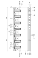
- 1 is a cross-sectional view of a semiconductor device according to a first embodiment.
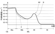
- 2 is a graph showing an impurity concentration distribution at the position of line AA in FIG. 1;
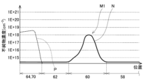
- 2 is a graph showing impurity concentration distributions at the positions of lines BB and CC in FIG. 1;
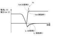
- 13 is a graph showing recovery characteristics when the switching speed of voltage Vak is slow.
- 13 is a graph showing recovery characteristics when the switching speed of voltage Vak is fast.
- 3A to 3C are explanatory diagrams of a manufacturing process of the semiconductor device according to the first embodiment.
- 3A to 3C are explanatory diagrams of a manufacturing process of the semiconductor device according to the first embodiment.
- 3A to 3C are explanatory diagrams of a manufacturing process of the semiconductor device according to the first embodiment.
- 3A to 3C are explanatory diagrams of a manufacturing process of the semiconductor device according to the first embodiment.
- 13 is a graph showing an impurity concentration distribution at the position of line AA of the semiconductor device of Example 2.
- 13 is a graph showing the impurity concentration distribution at the positions of lines BB and CC of the semiconductor device of Example 3.
- a mountain-shaped distribution of n-type impurity concentration along the thickness direction of the semiconductor substrate may be provided in the second cathode region.
- the mountain-shaped distribution in the second cathode region may have a peak value higher than 1 ⁇ 10 18 cm ⁇ 3 and lower than 1 ⁇ 10 19 cm ⁇ 3 .
- any of the above-mentioned semiconductor devices may be manufactured by the following manufacturing method.
- This manufacturing method may include an ion implantation step and a laser irradiation step.
- the collector region, the cathode region, and the surge suppression region may be formed by ion-implanting p-type impurities and n-type impurities into the lower surface of the semiconductor substrate.
- the laser irradiation step a laser may be irradiated onto the lower surface of the semiconductor substrate after the collector region, the cathode region, and the surge suppression region are formed.
- a heated area of 950°C or more may be formed in a surface layer portion near the lower surface of the semiconductor substrate. The thickness of the heated area may be thinner than the thickness of the cathode region.
- This manufacturing method can reduce the activation rate of n-type impurities in the second cathode region.
- the semiconductor device 10 of Example 1 shown in FIG. 1 has a semiconductor substrate 12.
- the semiconductor substrate 12 is made of silicon.
- the semiconductor substrate 12 may be made of a semiconductor material other than silicon.
- the semiconductor substrate 12 has an IGBT region 30 and a diode region 40.
- An IGBT is provided in the IGBT region 30, and a diode is provided in the diode region 40.
- the semiconductor device 10 is an RC-IGBT.
- a plurality of trenches 14 are provided on the upper surface 12a of the semiconductor substrate 12.
- the trenches 14 extend parallel to each other on the upper surface 12a.
- a plurality of trenches 14 are provided in each of the IGBT region 30 and the diode region 40.
- the inner surface of each trench 14 is covered with a gate insulating film 18.
- An electrode 16 is disposed in each trench 14.
- Each electrode 16 is insulated from the semiconductor substrate 12 by the gate insulating film 18.
- the electrode 16 in the IGBT region 30 is a gate electrode 16a.
- Each gate electrode 16a is connected to a gate pad (not shown).
- An external circuit is connected to the gate pad. The potential of each gate electrode 16a is controlled by the external circuit.
- the electrode 16 in the diode region 40 is a dummy electrode 16b.
- Each dummy electrode 16b may be connected to a gate pad, or may be connected to another electrode (e.g., the upper electrode 22) without being connected to the gate pad.
- the dummy electrode 16b When each dummy electrode 16b is connected to a gate pad, the dummy electrode 16b has the same potential as the gate electrode 16a.
- the potential of each dummy electrode 16b is independent of the gate electrode 16a.
- An interlayer insulating film 20 and an upper electrode 22 are provided on the upper part of the semiconductor substrate 12.
- the interlayer insulating film 20 covers the upper surfaces of the gate electrode 16a and the dummy electrode 16b.
- a plurality of contact holes 20a are provided in the interlayer insulating film 20. Each contact hole 20a is disposed in a position where no trench 14 exists.
- a plurality of contact holes 20a are provided in each of the IGBT region 30 and the diode region 40.
- the upper electrode 22 covers the interlayer insulating film 20 and the upper surface 12a of the semiconductor substrate 12.
- the upper electrode 22 contacts the upper surface 12a of the semiconductor substrate 12 in each contact hole 20a. Therefore, the upper electrode 22 contacts the upper surface 12a in each of the IGBT region 30 and the diode region 40.
- a lower electrode 24 is provided on the lower part of the semiconductor substrate 12.
- the lower electrode 24 covers the entire lower surface 12b of the semiconductor substrate 12. Therefore, the lower electrode 24 contacts the lower surface 12b in both the IGBT region 30 and the diode region 40.
- Each emitter region 52 has a high n-type impurity concentration.
- Each emitter region 52 is disposed in a region between trenches 14 (hereinafter referred to as inter-trench region).
- Each emitter region 52 is disposed in a range including the upper surface 12a of the semiconductor substrate 12.
- Each emitter region 52 is in ohmic contact with the upper electrode 22 in the corresponding contact hole 20a.
- Each emitter region 52 is in contact with the gate insulating film 18 at the upper end of the side surface of the corresponding trench 14.
- An upper p-type region is provided across the IGBT region 30 and the diode region 40.
- the upper p-type region in the IGBT region 30 is referred to as the body region 54
- the upper p-type region in the diode region 40 is referred to as the anode region 56.
- the upper p-type region contacts the upper electrode 22 at each contact hole 20a in the IGBT region 30 and the diode region 40.
- the body region 54 has a low concentration region 54b and a plurality of contact regions 54a. Each contact region 54a has a higher p-type impurity concentration than the low concentration region 54b. Each contact region 54a is disposed in a corresponding inter-trench region. Each contact region 54a is disposed in a range including the upper surface 12a of the semiconductor substrate 12. Each contact region 54a is in ohmic contact with the upper electrode 22 in the corresponding contact hole 20a.
- the low concentration region 54b is distributed across a plurality of inter-trench regions. The low concentration region 54b is disposed below the contact region 54a and the emitter region 52. Each emitter region 52 is separated from a drift region 58 described later by the low concentration region 54b.
- the low concentration region 54b contacts the gate insulating film 18 below each emitter region 52. Each gate electrode 16a faces the low concentration region 54b between the emitter region 52 and the drift region 58 via the gate insulating film 18.
- the anode region 56 has a low concentration region 56b and multiple contact regions 56a. Each contact region 56a has a higher p-type impurity concentration than the low concentration region 56b. Each contact region 56a is disposed in a corresponding inter-trench region. Each contact region 56a is disposed in an area including the upper surface 12a of the semiconductor substrate 12. Each contact region 56a is in ohmic contact with the upper electrode 22 in the corresponding contact hole 20a. The low concentration region 56b is distributed across multiple inter-trench regions. The low concentration region 56b is disposed below the contact region 54a.
- n-type drift region 58 is provided below the upper p-type region (i.e., the body region 54 and the anode region 56).
- the n-type impurity concentration of the drift region 58 is low.
- the drift region 58 is distributed across the IGBT region 30 and the diode region 40.
- the drift region 58 contacts the body region 54 and the anode region 56 from below.
- the drift region 58 contacts the gate insulating film 18 below the body region 54 and the anode region 56.
- a field stop region 60 is provided below the drift region 58.
- the field stop region 60 is an n-type region that has a higher n-type impurity concentration than the drift region 58.
- the field stop region 60 is distributed across the IGBT region 30 and the diode region 40.
- the field stop region 60 contacts the drift region 58 from below.
- an intermediate n-type region 62 and a collector region 64 are disposed below the field stop region 60.
- the collector region 64 is a p-type region having a high p-type impurity concentration.
- the collector region 64 is disposed in an area including the lower surface 12b of the semiconductor substrate 12, and is in ohmic contact with the lower electrode 24.
- the intermediate n-type region 62 is an n-type region having an n-type impurity concentration similar to that of the drift region 58.
- the intermediate n-type region 62 is disposed between the field stop region 60 and the collector region 64.
- each cathode region 66 is an n-type region having a higher n-type impurity concentration than the drift region 58.
- Each cathode region 66 is arranged in a range including the lower surface 12b of the semiconductor substrate 12.
- Each surge suppression region 70 is a p-type region having a high p-type impurity concentration. The p-type impurity concentration of each surge suppression region 70 is approximately equal to the p-type impurity concentration of the collector region 64.
- Each surge suppression region 70 is arranged in a range including the lower surface 12b of the semiconductor substrate 12.
- a plurality of cathode regions 66 and a plurality of surge suppression regions 70 are alternately arranged on the lower surface 12b of the semiconductor substrate 12 along a specific direction (in FIG. 1, a direction perpendicular to each trench 14).
- Each cathode region 66 and each surge suppression region 70 are in ohmic contact with the lower electrode 24.
- the intermediate n-type region 62 is disposed between the field stop region 60 and the surge suppression region 70.
- Each cathode region 66 has a first cathode region 66a having an n-type impurity concentration of 1 ⁇ 10 19 cm ⁇ 3 or more, and a second cathode region 66b having an n-type impurity concentration of less than 1 ⁇ 10 19 cm ⁇ 3 .
- the first cathode region 66a is disposed in a range including the lower surface 12b of the semiconductor substrate 12.
- the first cathode region 66a is in ohmic contact with the lower electrode 24.
- the second cathode region 66b is disposed between the first cathode region 66a and the field stop region 60.
- the second cathode region 66b is in contact with the field stop region 60 from below, and is in contact with the first cathode region 66a from above.
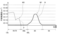
- FIG. 2 shows the impurity concentration distribution along line A-A in Figure 1
- Figure 3 shows the impurity concentration distribution along lines B-B and C-C in Figure 1. Note that the impurity concentration distributions along lines B-B and C-C are approximately equal.
- the horizontal axis indicates the position in the thickness direction of the semiconductor substrate, and the origin corresponds to the position of the lower surface 12b.
- graph N indicates the n-type impurity concentration distribution
- graph P indicates the p-type impurity concentration distribution.
- the n-type impurity concentration is low and distributed approximately uniformly within the drift region 58.
- the n-type impurity concentration forms a mountain-shaped distribution M1 in the thickness direction of the semiconductor substrate 12. That is, the field stop region 60 is a region in which the mountain-shaped distribution M1 in the thickness direction exists continuously from the IGBT region 30 to the diode region 40.
- the peak value of the n-type impurity concentration in the field stop region 60 is less than 1 ⁇ 10 19 cm -3 .
- the n-type impurity concentration is 1 ⁇ 10 19 cm ⁇ 3 or more in the first cathode region 66a.
- the n-type impurity concentration is distributed substantially uniformly at a high value (for example, about 1 ⁇ 10 20 cm ⁇ 3 in FIG. 2).
- the n-type impurity is distributed in a box profile.
- the second cathode region 66b is an n-type region between the field stop region 60 and the first cathode region 66a.
- the n-type impurity concentration in the second cathode region 66b is higher than the n-type impurity concentration at the lower end 60L of the field stop region 60 and is less than 1 ⁇ 10 19 cm ⁇ 3 .
- the n-type impurity concentration increases continuously from the upper side to the lower side in the second cathode region 66b.
- the n-type impurity concentration is uniformly distributed at a value similar to that in the drift region 58.
- the p-type impurity concentration is higher than the n-type impurity concentration.
- the p-type impurity is distributed in a box profile.
- Graph X in FIG. 2 shows the concentration distribution of activated n-type impurities. That is, while graph N shows the concentration distribution of n-type impurities that combines activated n-type impurities and non-activated n-type impurities, graph X shows the concentration distribution of activated n-type impurities.
- the value shown in graph X i.e., the concentration of activated n-type impurities
- the difference between graphs N and X corresponds to the concentration of non-activated n-type impurities. As shown in FIG. 2, the difference between graphs N and X is large in the second cathode region 66b.
- the activation rate of n-type impurities in the second cathode region 66b is 85% or less.
- the activation rate means the value obtained by dividing the total amount of activated n-type impurities in the target region by the total amount of n-type impurities present in the target region.
- the activation rate in the second cathode region 66b can be calculated by dividing the value obtained by integrating the graph X in the second cathode region 66b by the value obtained by integrating the graph N in the second cathode region 66b.
- the activation rate of n-type impurities is low in the second cathode region 66b, non-activated n-type impurities are present in the second cathode region 66b at a high concentration.
- Non-activated impurities in the semiconductor substrate 12 are a type of crystal defect and act as carrier recombination centers. Therefore, the carrier lifetime is short in the second cathode region 66b.
- the activation rate of n-type impurities is higher in the first cathode region 66a than in the second cathode region 66b.
- the activation rate of n-type impurities in the first cathode region 66a may be higher than 85%.
- the upper electrode 22 functions as the emitter electrode of the IGBT and also functions as the anode electrode of the diode.
- the lower electrode 24 functions as the collector electrode of the IGBT and also functions as the cathode electrode of the diode.
- the semiconductor device 10 When the semiconductor device 10 operates as an IGBT, a higher potential is applied to the lower electrode 24 than to the upper electrode 22.
- a potential equal to or higher than the gate threshold is applied to the gate electrode 16a, a channel is formed in the low concentration region 54b in the area adjacent to the gate insulating film 18, and the channel connects the emitter region 52 and the drift region 58.
- the IGBT is turned on, and electrons flow from the emitter region 52 through the channel into the drift region 58.
- the IGBT when the IGBT is turned on, holes flow from the collector region 64 into the drift region 58. This reduces the resistance of the drift region 58, and electrons flow through the drift region 58 with low resistance. After passing through the drift region 58, the electrons flow into the collector region 64.
- the cathode region 66 and the surge suppression region 70 are alternately provided in the diode region 40, and the area ratio of the cathode region 66 on the lower surface 12b is low. For this reason, it is difficult for electrons to flow from the drift region 58 to the cathode region 66 when the IGBT turns on. This suppresses snapback.
- the semiconductor device 10 When the semiconductor device 10 operates as a diode, a higher potential is applied to the upper electrode 22 than to the lower electrode 24. In this state, electrons flow from the cathode region 66 into the drift region 58. Holes also flow from the anode region 56 into the drift region 58. This reduces the resistance of the drift region 58, and electrons flow through the drift region 58 with low resistance. After passing through the drift region 58, the electrons flow into the anode region 56. After passing through the drift region 58, the holes flow into the cathode region 66.
- the voltage Vak between the upper electrode 22 and the lower electrode 24 may switch from a forward voltage (i.e., a voltage at which the potential of the upper electrode 22 is higher than that of the lower electrode 24) to a reverse voltage (i.e., a voltage at which the potential of the lower electrode 24 is higher than that of the upper electrode 22).
- a forward voltage i.e., a voltage at which the potential of the upper electrode 22 is higher than that of the lower electrode 24
- a reverse voltage i.e., a voltage at which the potential of the lower electrode 24 is higher than that of the upper electrode 22.
- FIG. 4 shows a comparison of the recovery characteristics of the diode of Example 1 and the diode of Comparative Example 1 when the switching speed of the voltage Vak is slow.
- the diode of Comparative Example 1 differs from the diode of Example 1 in that the activation rate of the n-type impurity in the second cathode region 66b is high.
- the voltage Vak is shown with the higher potential of the cathode (i.e., the lower electrode 24) as positive.
- the graphs of the voltage Vak are overlapped between Example 1 and Comparative Example 1.
- the current I F indicates the current flowing through the diode.
- a positive value indicates a current flowing in the forward direction
- a negative value indicates a current flowing in the reverse direction.
- the current I F is negative when the recovery state is in effect.
- the recovery state holes present in the drift region 58, the field stop region 60, and the cathode region 66 are discharged to the upper electrode 22 via the anode region 56. Holes present closer to the anode region 56 are more likely to be discharged to the upper electrode 22. Therefore, it takes time for holes present in the cathode region 66 to be discharged to the upper electrode 22.
- a recovery current flows until the holes present in the cathode region 66 are discharged to the upper electrode 22, so the recovery current is less likely to decay.
- the activation rate of the n-type impurities in the second cathode region 66b is low, so the carrier lifetime in the second cathode region 66b is short. Therefore, many holes disappear in the second cathode region 66b by recombination with electrons. Therefore, in the diode of Example 1, the recovery current decays faster than in the diode of Comparative Example 1. Therefore, in the diode of Example 1, recovery loss is less likely to occur. It should be noted that the surge suppression region 70 has almost no effect on the characteristics of the diode when the switching speed of the voltage Vak is slow.
- (When the switching speed of the voltage Vak is fast) 5 shows a comparison of the recovery characteristics of the diode of Example 1 and the diode of Comparative Example 2 when the switching speed of the voltage Vak is fast.
- the diode of Comparative Example 2 has a low activation rate of n-type impurities in the second cathode region 66b, similar to the diode of Example 1.
- the diode of Comparative Example 2 differs from the diode of Example 1 in that it does not have the surge suppression region 70.
- the activation rate of the n-type impurities in the second cathode region 66b is low, so the recovery current is easily attenuated. For this reason, when the switching speed of the voltage Vak is fast, the recovery current decays extremely fast, as shown in FIG. 5. As a result, a surge voltage Vs occurs during recovery operation due to the influence of the parasitic inductance of the electric circuit.
- the diode of Example 1 when the switching speed of the voltage Vak is fast, holes flow from the surge suppression region 70 into the drift region 58. The flow of holes into the drift region 58 slows down the decay rate of the recovery current. This prevents the decay rate of the recovery current from becoming excessively fast, as shown in FIG. 5, and suppresses the surge voltage.
- the second cathode region 66b promotes the decay of the recovery current, thereby reducing the recovery loss.
- the surge suppression region 70 prevents the decay speed of the recovery current from becoming excessively fast, thereby suppressing the surge voltage.
- the structure of the upper surface side of the semiconductor device 10 and the field stop region 60 are formed.
- p-type impurities are injected into the entire lower surface 12b of the semiconductor substrate 12 to form a p-type region 72 in the surface layer near the lower surface 12b.
- the p-type region 72 is a p-type region that corresponds to the collector region 64 and the surge suppression region 70.
- n-type impurities are injected into a part of the lower surface 12b (i.e., the range corresponding to the cathode region 66) at a higher concentration than the p-type impurity concentration of the p-type region 72 to form the cathode region 66.
- the cathode region 66 is made thicker than the p-type region 72.
- the p-type region 72 remaining after the formation of the cathode region 66 becomes the collector region 64 and the surge suppression region 70.
- the lower surface 12b of the semiconductor substrate 12 is heated by irradiating the laser L so as to scan the entire lower surface 12b of the semiconductor substrate 12.
- a green laser with a wavelength of 532 nm is used as the laser L.
- the surface layer of the semiconductor substrate 12 near the lower surface 12b is heated to a temperature of 950°C or higher.
- the heated range 94 the range heated to a temperature of 950°C or higher by irradiation with the laser L is referred to as the heated range 94.
- the semiconductor substrate 12 temporarily melts. When the semiconductor substrate 12 temporarily melts, impurities are uniformly diffused within the heated range 94.
- a first cathode region 66a having a box profile, a surge suppression region 70, and a collector region 64 are formed within the heated range 94.
- the heated range 94 is controlled so that the thickness of the heated range 94 is thinner than the thickness of the cathode region 66. Therefore, the portion of the cathode region 66 above the heating range 94 becomes the second cathode region 66b, which has a lower n-type impurity concentration than the first cathode region 66a. Because the second cathode region 66b is not included in the heating range 94, the n-type impurities in the second cathode region 66b are difficult to activate. Therefore, the second cathode region 66b with a low activation rate is formed.
- the lower electrode 24 is formed to complete the semiconductor device shown in FIG. 1. Since the first cathode region 66a, the surge suppression region 70, and the collector region 64 have a high impurity concentration, these regions contact the lower electrode 24 with low contact resistance.
- the activation rate of the n-type impurity in the first cathode region 66a is not very high, but this is because the n-type impurity concentration in the first cathode region 66a is close to the solid solubility limit.
- the activation rate of the n-type impurity is low, even though the n-type impurity concentration is not very high. This is because the second cathode region 66b is not included in the heating range 94 during the laser irradiation process.
- Example 10 shows the impurity concentration distribution at the position of line A-A of the semiconductor device of Example 2.
- a mountain-shaped distribution M2 of n-type impurity concentration is formed in the second cathode region 66b.
- the peak value of the n-type impurity concentration in the mountain-shaped distribution M2 is higher than 1 ⁇ 10 18 cm -3 and lower than 1 ⁇ 10 19 cm -3 .
- the other configurations of Example 2 are the same as those of Example 1.
- the mountain-shaped distribution M2 can be formed by locally implanting the n-type impurity at a high concentration within the depth range of the second cathode region 66b.
- the n-type impurity concentration in the second cathode region 66b increases, and the activation rate of the n-type impurity in the second cathode region 66b can be made lower. This makes it possible to shorten the carrier lifetime in the second cathode region 66b. This makes it possible to more effectively suppress the recovery loss of the diode.
- FIG. 11 shows the impurity concentration distribution at the positions of lines B-B and C-C of the semiconductor device of Example 3.
- the collector region 64 and the surge suppression region 70 have a mountain-shaped distribution M3 on the upper side of the box profile.
- the other configurations of Example 3 are the same as those of Example 1.
- the p-type impurities are injected so as to have a peak above the heating range 94, thereby forming the mountain-shaped distribution M3.
- the collector region 64 and the surge suppression region 70 can be made thicker than in Example 1.
- Example 1 the thickness of the collector region 64 and the surge suppression region 70 was about the same as or thinner than the first cathode region 66a. However, according to Example 3, the thickness of the collector region 64 and the surge suppression region 70 can be made thicker than the first cathode region 66a.
- the gate electrode of the IGBT is a trench type, but the gate electrode of the IGBT may be a planar type.
Landscapes
- Metal-Oxide And Bipolar Metal-Oxide Semiconductor Integrated Circuits (AREA)
Abstract
RC-IGBTにおいて、リカバリ損失を低減しながら、サージ電圧を抑制する。半導体装置であって、IGBT領域とダイオード領域に跨って分布しているn型のフィールドストップ領域と、前記IGBT領域内で前記フィールドストップ領域の下側に配置されているp型のコレクタ領域と、前記ダイオード領域内で前記フィールドストップ領域の下側に配置されている複数のn型のカソード領域と、前記ダイオード領域内で前記フィールドストップ領域の下側に配置されている複数のp型のサージ抑制領域、を有する。前記各カソード領域が、前記下部電極に接しているとともに1×1019cm-3以上のn型不純物濃度を有する第1カソード領域と、前記第1カソード領域と前記フィールドストップ領域の間に配置されているとともにn型不純物の活性化率が85%以下である第2カソード領域、を有する。
Description
(関連出願の相互参照)
本出願は、2023年5月11日に出願された日本特許出願特願2023-078489の関連出願であり、この日本特許出願に基づく優先権を主張するものであり、この日本特許出願に記載された全ての内容を、本明細書を構成するものとして援用する。
本出願は、2023年5月11日に出願された日本特許出願特願2023-078489の関連出願であり、この日本特許出願に基づく優先権を主張するものであり、この日本特許出願に記載された全ての内容を、本明細書を構成するものとして援用する。
本明細書に開示の技術は、半導体装置とその製造方法に関する。
日本特許特開2015-211149号公報(以下、特許文献1という)には、絶縁ゲートバイポーラトランジスタとダイオードを有する半導体装置の製造方法が開示されている。以下では、絶縁ゲートバイポーラトランジスタをIGBT(すなわち、Insulated Gate Bipolar Transistor)という場合がある。また、以下では、IGBTとダイオードを有する半導体装置を、RC-IGBTという場合がある。特許文献1の製造方法では、n型不純物のイオン注入によってn型のカソード領域を形成する。次に、半導体基板にヘリウムイオンを照射することによって、カソード領域内に結晶欠陥を形成する。カソード領域内に結晶欠陥を形成することで、IGBTがターンオンするときにスナップバックを抑制できる。
ダイオードに対する印加電圧が順電圧から逆電圧に切り換わると、ダイオードの内部に存在するホールがアノード電極に排出される。これによって、ダイオードに逆方向にリカバリ電流が流れる。特許文献1のRC-IGBTでは、カソード領域内の結晶欠陥が再結合中心として機能する。このため、リカバリ動作時にホールが結晶欠陥において再結合により消滅し、リカバリ電流が早期に減衰する。これにより、ダイオードのリカバリ損失が低減される。
ダイオードに対する印加電圧が高速で変化する場合がある。ダイオードに対する印加電圧が順電圧から逆電圧に高速で切り換わる場合に、リカバリ電流の減衰速度が過度に速くなることでサージ電圧が発生する場合がある。カソード領域内に結晶欠陥が存在すると、リカバリ電流が減衰し易いので、サージ電圧が発生し易い。
以上に説明したように、カソード領域内に結晶欠陥が存在すると、リカバリ損失を低減できる一方で、印加電圧が高速で変化する場合にサージ電圧が発生し易い。本明細書では、RC-IGBTにおいて、リカバリ損失を低減しながら、サージ電圧を抑制する技術を提案する。
本明細書が開示する半導体装置は、IGBT領域とダイオード領域とを有する半導体基板と、前記IGBT領域内と前記ダイオード領域内で前記半導体基板の上面に接する上部電極と、前記IGBT領域内と前記ダイオード領域内で前記半導体基板の下面に接する下部電極と、ゲート電極を有する。前記半導体基板は、エミッタ領域と、上部p型領域と、ドリフト領域と、フィールドストップ領域と、コレクタ領域と、複数のカソード領域と、複数のサージ抑制領域、を有する。前記エミッタ領域は、前記IGBT領域内で前記上部電極に接するn型領域である。前記上部p型領域は、前記IGBT領域と前記ダイオード領域に跨って分布しており、前記IGBT領域内と前記ダイオード領域内で前記上部電極に接している。前記ドリフト領域は、前記上部p型領域の下側に配置されており、前記IGBT領域と前記ダイオード領域に跨って分布しており、前記上部p型領域によって前記エミッタ領域から分離されているn型領域である。前記フィールドストップ領域は、前記ドリフト領域の下側に配置されており、前記ドリフト領域よりも高いn型不純物濃度を有しており、前記半導体基板の厚み方向に沿うn型不純物濃度分布において山型分布を有し、前記IGBT領域と前記ダイオード領域に跨って分布しているn型領域である。前記コレクタ領域は、前記IGBT領域内に配置されており、前記フィールドストップ領域の下側に配置されており、前記下部電極に接するp型領域である。複数の前記カソード領域は、前記ダイオード領域内に配置されており、前記フィールドストップ領域の下側に配置されており、前記下部電極に接するn型領域である。複数の前記サージ抑制領域は、前記ダイオード領域内に配置されており、前記フィールドストップ領域の下側に配置されており、前記下部電極に接するp型領域である。前記ゲート電極が、前記エミッタ領域と前記ドリフト領域の間の前記上部p型領域に対してゲート絶縁膜を介して対向している。前記ダイオード領域内では、前記半導体基板の前記下面において、特定方向に沿って複数の前記カソード領域と複数の前記サージ抑制領域が交互に配置されている。前記各カソード領域が、前記下部電極に接しているとともに1×1019cm-3以上のn型不純物濃度を有する第1カソード領域と、前記第1カソード領域と前記フィールドストップ領域の間に配置されているとともにn型不純物の活性化率が85%以下である第2カソード領域、を有する。
なお、本明細書において、上部p型領域は、IGBT領域とダイオード領域に跨って分布しているとともにIGBT領域内とダイオード領域内で上部電極に接しているp型領域であれば、どのようなp型領域であってもよい。例えば、IGBT領域内の上部p型領域とダイオード領域内の上部p型領域とで、p型不純物の濃度プロファイルが等しくてもよいし、p型不純物の濃度プロファイルが異なっていてもよい。
この半導体装置では、上部電極がIGBTのエミッタ電極として機能するとともにダイオードのアノード電極として機能する。また、下部電極がIGBTのコレクタ電極として機能するとともにダイオードのカソード電極として機能する。カソード領域は、第1カソード領域と第2カソード領域を有する。第1カソード領域が1×1019cm-3以上のn型不純物濃度を有するので、第1カソード領域は低い接触抵抗で下部電極に接している。したがって、ダイオードがオンするときに損失が生じ難い。また、第2カソード領域ではn型不純物の活性化率が85%以下であるので、第2カソード領域内には活性化していないn型不純物が多く存在する。第2カソード領域内の活性化していないn型不純物は、結晶欠陥を構成するので、ホールの再結合中心として機能する。また、ダイオード領域内には、カソード領域の隣にp型のサージ抑制領域が配置されている。ダイオードに対する印加電圧が順電圧から逆電圧に高速で切り換わると、ダイオードにリカバリ電流が流れる。第2カソード領域内の結晶欠陥(すなわち、活性化していないn型不純物)はリカバリ電流を減衰させるように作用する。他方、ダイオードに対する印加電圧が順電圧から逆電圧に高速で切り換わると、サージ抑制領域からドリフト領域にホールが注入される。このようにドリフト領域にホールが注入されると、リカバリ電流が減衰し難くなる。したがって、ダイオードに対する印加電圧が順電圧から逆電圧に高速で切り換わる場合には、リカバリ電流の急速な減衰が抑制され、サージ電圧の発生が抑制される。また、ダイオードに対する印加電圧が順電圧から逆電圧に通常の速度で切り換わる場合には、サージ抑制領域からドリフト領域へのホールの注入はほとんど生じない。したがって、この場合には、第2カソード領域内の結晶欠陥がリカバリ電流を早期に減衰させる。したがって、リカバリ損失を低減できる。このように、この半導体装置によれば、通常のリカバリ動作ではリカバリ損失を低減でき、印加電圧が急速に切り換わる場合にはサージ電圧を抑制できる。
本明細書が開示する一例の形態では、前記第2カソード領域内に、前記半導体基板の厚み方向に沿うn型不純物濃度分布において山型分布が設けられていてもよい。
このように第2カソード領域内のn型不純物濃度を高くすると、第2カソード領域内の活性化率をより低くすることができる。したがって、リカバリ損失をより効果的に抑制できる。
前記第2カソード領域内に設けられた前記山型分布が、1×1018cm-3より高く1×1019cm-3より低いピーク値を有していてもよい。
上述したいずれかの半導体装置は、以下の製造方法により製造されてもよい。この製造方法は、イオン注入工程とレーザ照射工程を有していてもよい。前記イオン注入工程では、前記半導体基板の前記下面にp型不純物とn型不純物をイオン注入することによって、前記コレクタ領域、前記カソード領域、及び、前記サージ抑制領域を形成してもよい。前記レーザ照射工程では、前記コレクタ領域、前記カソード領域、及び、前記サージ抑制領域の形成後に、前記半導体基板の前記下面にレーザを照射してもよい。前記レーザを照射する前記工程では、前記半導体基板の前記下面の近傍の表層部に950℃以上の加熱範囲を形成してもよい。前記加熱範囲の厚さが、前記カソード領域の厚さよりも薄くてもよい。
この製造方法によれば、第2カソード領域内のn型不純物の活性化率を低くすることができる。
図1に示す実施例1の半導体装置10は、半導体基板12を有している。半導体基板12は、シリコンによって構成されている。但し、半導体基板12がシリコン以外の半導体材料によって構成されていてもよい。半導体基板12は、IGBT領域30とダイオード領域40を有している。IGBT領域30にはIGBTが設けられており、ダイオード領域40にはダイオードが設けられている。すなわち、半導体装置10はRC-IGBTである。
半導体基板12の上面12aには、複数のトレンチ14が設けられている。各トレンチ14は、上面12aにおいて互いに平行に伸びている。IGBT領域30とダイオード領域40のそれぞれに複数のトレンチ14が設けられている。各トレンチ14の内面は、ゲート絶縁膜18によって覆われている。各トレンチ14内に電極16が配置されている。各電極16は、ゲート絶縁膜18によって半導体基板12から絶縁されている。IGBT領域30内の電極16は、ゲート電極16aである。各ゲート電極16aは、図示しないゲートパッドに接続されている。ゲートパッドには、外部回路が接続される。各ゲート電極16aの電位は、外部回路によって制御される。ダイオード領域40内の電極16は、ダミー電極16bである。各ダミー電極16bは、ゲートパッドに接続されていてもよいし、ゲートパッドに接続されずに他の電極(例えば、上部電極22)に接続されていてもよい。各ダミー電極16bがゲートパッドに接続されている場合には、各ダミー電極16bはゲート電極16aと同じ電位を有する。各ダミー電極16bがゲートパッドに接続されていない場合には、各ダミー電極16bの電位はゲート電極16aから独立している。
半導体基板12の上部に、層間絶縁膜20と上部電極22が設けられている。層間絶縁膜20は、ゲート電極16a及びダミー電極16bの上面を覆っている。層間絶縁膜20には、複数のコンタクトホール20aが設けられている。各コンタクトホール20aは、トレンチ14が存在しない位置に配置されている。IGBT領域30とダイオード領域40のそれぞれに複数のコンタクトホール20aが設けられている。上部電極22は、層間絶縁膜20と半導体基板12の上面12aを覆っている。上部電極22は、各コンタクトホール20a内で半導体基板12の上面12aに接している。したがって、上部電極22は、IGBT領域30とダイオード領域40のそれぞれで上面12aに接している。
半導体基板12の下部に、下部電極24が設けられている。下部電極24は、半導体基板12の下面12bの全域を覆っている。したがって、下部電極24は、IGBT領域30とダイオード領域40のそれぞれで下面12bに接している。
IGBT領域30内には、複数のn型のエミッタ領域52が設けられている。各エミッタ領域52は、高いn型不純物濃度を有している。各エミッタ領域52は、トレンチ14の間の領域(以下、トレンチ間領域という)に配置されている。各エミッタ領域52は、半導体基板12の上面12aを含む範囲に配置されている。各エミッタ領域52は、対応するコンタクトホール20aにおいて、上部電極22にオーミック接触している。各エミッタ領域52は、対応するトレンチ14の側面の上端部においてゲート絶縁膜18に接している。
IGBT領域30とダイオード領域40に跨って、上部p型領域が設けられている。以下では、IGBT領域30内の上部p型領域をボディ領域54と呼び、ダイオード領域40内の上部p型領域をアノード領域56という。上部p型領域は、IGBT領域30及びダイオード領域40内の各コンタクトホール20aにおいて上部電極22に接している。
ボディ領域54は、低濃度領域54bと複数のコンタクト領域54aを有している。各コンタクト領域54aは、低濃度領域54bよりも高いp型不純物濃度を有している。各コンタクト領域54aは、対応するトレンチ間領域に配置されている。各コンタクト領域54aは、半導体基板12の上面12aを含む範囲に配置されている。各コンタクト領域54aは、対応するコンタクトホール20aにおいて、上部電極22にオーミック接触している。低濃度領域54bは、複数のトレンチ間領域に跨って分布している。低濃度領域54bは、コンタクト領域54aとエミッタ領域52の下側に配置されている。低濃度領域54bによって、各エミッタ領域52は後述するドリフト領域58から分離されている。低濃度領域54bは、各エミッタ領域52の下側でゲート絶縁膜18に接している。各ゲート電極16aは、エミッタ領域52とドリフト領域58の間の低濃度領域54bに対してゲート絶縁膜18を介して対向している。
アノード領域56は、低濃度領域56bと複数のコンタクト領域56aを有している。各コンタクト領域56aは、低濃度領域56bよりも高いp型不純物濃度を有している。各コンタクト領域56aは、対応するトレンチ間領域に配置されている。各コンタクト領域56aは、半導体基板12の上面12aを含む範囲に配置されている。各コンタクト領域56aは、対応するコンタクトホール20aにおいて、上部電極22にオーミック接触している。低濃度領域56bは、複数のトレンチ間領域に跨って分布している。低濃度領域56bは、コンタクト領域54aの下側に配置されている。
上部p型領域(すなわち、ボディ領域54とアノード領域56)の下側に、n型のドリフト領域58が設けられている。ドリフト領域58のn型不純物濃度は低い。ドリフト領域58は、IGBT領域30とダイオード領域40に跨って分布している。ドリフト領域58は、ボディ領域54及びアノード領域56に対して下側から接している。ドリフト領域58は、ボディ領域54及びアノード領域56の下側でゲート絶縁膜18に接している。
ドリフト領域58の下側に、フィールドストップ領域60が設けられている。フィールドストップ領域60は、ドリフト領域58よりも高いn型不純物濃度を有するn型領域である。フィールドストップ領域60は、IGBT領域30とダイオード領域40に跨って分布している。フィールドストップ領域60は、ドリフト領域58に対して下側から接している。
IGBT領域30内では、フィールドストップ領域60の下側に中間n型領域62とコレクタ領域64が配置されている。コレクタ領域64は、高いp型不純物濃度を有するp型領域である。コレクタ領域64は、半導体基板12の下面12bを含む範囲に配置されており、下部電極24に対してオーミック接触している。中間n型領域62は、ドリフト領域58と同程度のn型不純物濃度を有するn型領域である。IGBT領域30内では、中間n型領域62はフィールドストップ領域60とコレクタ領域64の間に配置されている。
ダイオード領域40内では、フィールドストップ領域60の下側に複数の中間n型領域62、複数のカソード領域66及び複数のサージ抑制領域70が配置されている。各カソード領域66は、ドリフト領域58よりも高いn型不純物濃度を有するn型領域である。各カソード領域66は、半導体基板12の下面12bを含む範囲に配置されている。各サージ抑制領域70は、高いp型不純物濃度を有するp型領域である。各サージ抑制領域70のp型不純物濃度は、コレクタ領域64のp型不純物濃度と略等しい。各サージ抑制領域70は、半導体基板12の下面12bを含む範囲に配置されている。ダイオード領域40内では、半導体基板12の下面12bにおいて、特定方向(図1では、各トレンチ14と直交する方向)に沿って複数のカソード領域66と複数のサージ抑制領域70が交互に配置されている。各カソード領域66と各サージ抑制領域70は、下部電極24に対してオーミック接触している。ダイオード領域40内では、中間n型領域62はフィールドストップ領域60とサージ抑制領域70の間に配置されている。
各カソード領域66は、1×1019cm-3以上のn型不純物濃度を有する第1カソード領域66aと、1×1019cm-3未満のn型不純物濃度を有する第2カソード領域66bを有している。第1カソード領域66aは、半導体基板12の下面12bを含む範囲に配置されている。第1カソード領域66aは、下部電極24に対してオーミック接触している。第2カソード領域66bは、第1カソード領域66aとフィールドストップ領域60の間に配置されている。第2カソード領域66bは、フィールドストップ領域60に対して下側から接しているとともに、第1カソード領域66aに対して上側から接している。
次に、ドリフト領域58、フィールドストップ領域60、中間n型領域62、コレクタ領域64、カソード領域66及びサージ抑制領域70内の不純物濃度分布について説明する。図2は図1のA-A線における不純物濃度分布であり、図3は図1のB-B線及びC-C線における不純物濃度分布である。なお、B-B線とC-C線では不純物濃度分布は略等しい。図2、3において、横軸は半導体基板の厚み方向における位置を示しており、原点が下面12bの位置に対応する。また、図2、3において、グラフNはn型不純物濃度分布を示し、グラフPはp型不純物濃度分布を示す。
図2、3に示すように、ドリフト領域58内では、n型不純物濃度が低い値で略均一に分布している。
図2、3に示すように、フィールドストップ領域60内では、半導体基板12の厚み方向において、n型不純物濃度が山型分布M1を形成している。すなわち、厚み方向における山型分布M1がIGBT領域30からダイオード領域40にかけて連続的に存在している領域がフィールドストップ領域60である。フィールドストップ領域60内のn型不純物濃度のピーク値は、1×1019cm-3未満である。
図2に示すように、第1カソード領域66a内では、n型不純物濃度が1×1019cm-3以上である。第1カソード領域66a内では、n型不純物濃度が高い値(例えば、図2では1×1020cm-3程度)で略一定で分布している。言い換えると、第1カソード領域66a内では、ボックスプロファイルでn型不純物が分布している。第2カソード領域66bはフィールドストップ領域60と第1カソード領域66aの間のn型領域である。第2カソード領域66b内のn型不純物濃度は、フィールドストップ領域60の下端60Lにおけるn型不純物濃度よりも高く、かつ、1×1019cm-3未満である。図2では、第2カソード領域66b内において、上側から下側に向かってn型不純物濃度が連続的に上昇している。
図3に示すように、中間n型領域62、コレクタ領域64及びサージ抑制領域70内では、n型不純物濃度がドリフト領域58内と同程度の値で均一に分布している。コレクタ領域64及びサージ抑制領域70内では、p型不純物濃度がn型不純物濃度よりも高い。コレクタ領域64及びサージ抑制領域70内では、ボックスプロファイルでp型不純物が分布している。
図2のグラフXは、活性化しているn型不純物の濃度分布を示している。すなわち、グラフNは、活性化しているn型不純物と活性化していないn型不純物を合わせたn型不純物の濃度分布を示している一方で、グラフXは、活性化しているn型不純物の濃度分布を示している。なお、グラフXに示す値(すなわち、活性化しているn型不純物の濃度)は、半導体基板12中の抵抗の分布を厚み方向に沿って測定し、その測定結果から算出した値である。グラフNとグラフXの差は、活性化していないn型不純物の濃度に相当する。図2に示すように、第2カソード領域66b内において、グラフNとグラフXの差が大きい。第2カソード領域66b内におけるn型不純物の活性化率は、85%以下である。なお、本明細書において、活性化率は、対象の領域中において活性化しているn型不純物の総量を、対象の領域に存在するn型不純物の総量で除算した値を意味する。例えば、グラフXを第2カソード領域66b内で積分した値を、グラフNを第2カソード領域66b内で積分した値によって除算することで、第2カソード領域66b内の活性化率を算出することができる。第2カソード領域66b内ではn型不純物の活性化率が低いので、第2カソード領域66b内には活性化していないn型不純物が高濃度で存在する。半導体基板12中で活性化していない不純物は、結晶欠陥の一種であり、キャリアの再結合中心として作用する。したがって、第2カソード領域66b内ではキャリアライフタイムが短い。図2に示すように、第1カソード領域66a内では、第2カソード領域66b内よりもn型不純物の活性化率が高い。例えば、第1カソード領域66a内におけるn型不純物の活性化率が85%より高くてもよい。
次に、半導体装置10の動作について説明する。上部電極22はIGBTのエミッタ電極として機能するとともにダイオードのアノード電極として機能する。下部電極24はIGBTのコレクタ電極として機能するとともにダイオードのカソード電極として機能する。
半導体装置10がIGBTとして動作する場合には、下部電極24に対して上部電極22よりも高い電位が印加される。ゲート電極16aにゲート閾値以上の電位を印加すると、ゲート絶縁膜18に隣接する範囲で低濃度領域54bにチャネルが形成され、チャネルによってエミッタ領域52とドリフト領域58が接続される。このため、IGBTがオンし、エミッタ領域52からチャネルを介してドリフト領域58に電子が流入する。また、IGBTがオンすると、コレクタ領域64からドリフト領域58にホールが流入する。これによって、ドリフト領域58の抵抗が低下し、電子がドリフト領域58内を低抵抗で流れる。電子は、ドリフト領域58を通過した後にコレクタ領域64へ流れる。
RC-IGBTでは、IGBTのターンオンの開始時(すなわち、チャネルの抵抗が高い状態のとき)に、ドリフト領域58からカソード領域66に電子が流れる。この状態では、IGBTのオン電圧は高い。その後、チャネルの抵抗が低下すると、ドリフト領域58からコレクタ領域64へ電子が流れるようになり、IGBTのオン電圧が低下する。このように、ターンオンの開始時においてオン電圧が一時的に高くなる現象は、スナップバックと呼ばれる。実施例1の半導体装置では、ダイオード領域40内においてカソード領域66とサージ抑制領域70が交互に設けられており、下面12bにおけるカソード領域66の面積比率が低い。このため、IGBTのターンオン時にドリフト領域58からカソード領域66へ電子が流れ難い。これによって、スナップバックが抑制される。
半導体装置10がダイオードとして動作する場合には、上部電極22に対して下部電極24よりも高い電位が印加される。この状態では、カソード領域66からドリフト領域58に電子が流入する。また、アノード領域56からドリフト領域58にホールが流入する。これによって、ドリフト領域58の抵抗が低下し、電子がドリフト領域58内を低抵抗で流れる。電子は、ドリフト領域58を通過した後にアノード領域56へ流れる。ホールは、ドリフト領域58を通過した後にカソード領域66へ流れる。
半導体装置10がダイオードとして動作している状態において、上部電極22と下部電極24の間の電圧Vakが、順電圧(すなわち、上部電極22の電位が下部電極24の電位よりも高くなる電圧)から逆電圧(すなわち、下部電極24の電位が上部電極22の電位よりも高くなる電圧)に切り換わる場合がある。このように電圧Vakが切り換わると、ダイオードがリカバリ動作を行う。ダイオードのリカバリ動作では、ドリフト領域58、フィールドストップ領域60及びカソード領域66中に存在するホールが、アノード領域56を介して上部電極22へ排出される。このようにホールが流れることで、ダイオードに瞬間的に逆電流(いわゆる、リカバリ電流)が流れる。リカバリ電流を早期に減衰させることで、リカバリ損失を抑制することができる。他方、リカバリ電流の減衰速度が速すぎると、リカバリ電流の急速な変化に伴ってサージ電圧が発生する。実施例1の半導体装置では電圧Vakが切り換わる速度が速い場合と遅い場合とでダイオードの動作が変化し、これによってリカバリ損失の低減とサージの抑制の両方が実現される。以下に、電圧Vakが切り換わる速度が遅い場合と速い場合のそれぞれについて、実施例1の半導体装置の動作を説明する。
(電圧Vakの切り換え速度が遅い場合)
図4は、電圧Vakの切り換え速度が遅い場合において、実施例1のダイオードと比較例1のダイオードのリカバリ特性を比較して示している。比較例1のダイオードは、第2カソード領域66b内のn型不純物の活性化率が高い点で実施例1のダイオードとは異なる。図4において、電圧Vakはカソード(すなわち、下部電極24)の電位が高い方をプラスとして示している。図4では、電圧Vakのグラフが実施例1と比較例1とで重なっている。図4において、電流IFはダイオードに流れる電流を示している。正の値は順方向に流れる電流を示し、負の値は逆方向に流れる電流を示している。
図4は、電圧Vakの切り換え速度が遅い場合において、実施例1のダイオードと比較例1のダイオードのリカバリ特性を比較して示している。比較例1のダイオードは、第2カソード領域66b内のn型不純物の活性化率が高い点で実施例1のダイオードとは異なる。図4において、電圧Vakはカソード(すなわち、下部電極24)の電位が高い方をプラスとして示している。図4では、電圧Vakのグラフが実施例1と比較例1とで重なっている。図4において、電流IFはダイオードに流れる電流を示している。正の値は順方向に流れる電流を示し、負の値は逆方向に流れる電流を示している。
図4において、電流IFが負であるときがリカバリ状態である。リカバリ状態では、ドリフト領域58、フィールドストップ領域60及びカソード領域66内に存在するホールがアノード領域56を介して上部電極22へ排出される。アノード領域56に近い位置に存在するホールほど上部電極22へ排出され易い。したがって、カソード領域66内に存在するホールは、上部電極22へ排出されるまでに時間を要する。比較例1のダイオードでは、カソード領域66内に存在するホールが上部電極22へ排出されるまでリカバリ電流が流れるので、リカバリ電流が減衰し難い。これに対し、実施例1のダイオードでは、第2カソード領域66bのn型不純物の活性化率が低いので、第2カソード領域66b内におけるキャリアライフタイムが短い。したがって、第2カソード領域66b内で多くのホールが電子との再結合によって消滅する。このため、実施例1のダイオードでは、比較例1のダイオードよりも、リカバリ電流が速く減衰する。したがって、実施例1のダイオードでは、リカバリ損失が生じ難い。なお、サージ抑制領域70は、電圧Vakの切り換え速度が遅い場合のダイオードの特性にほとんど影響を与えない。
(電圧Vakの切り換え速度が速い場合)
図5は、電圧Vakの切り換え速度が速い場合において、実施例1のダイオードと比較例2のダイオードのリカバリ特性を比較して示している。比較例2のダイオードでは、実施例1のダイオードと同様に、第2カソード領域66b内のn型不純物の活性化率が低い。比較例2のダイオードは、サージ抑制領域70を有さない点で実施例1のダイオードとは異なる。
図5は、電圧Vakの切り換え速度が速い場合において、実施例1のダイオードと比較例2のダイオードのリカバリ特性を比較して示している。比較例2のダイオードでは、実施例1のダイオードと同様に、第2カソード領域66b内のn型不純物の活性化率が低い。比較例2のダイオードは、サージ抑制領域70を有さない点で実施例1のダイオードとは異なる。
比較例2のダイオードでは、第2カソード領域66b内のn型不純物の活性化率が低いので、リカバリ電流が減衰し易い。このため、電圧Vakの切り換え速度が速い場合に、図5に示すようにリカバリ電流の減衰速度が極めて速くなる。その結果、電気回路の寄生インダクタンスの影響により、リカバリ動作時にサージ電圧Vsが発生する。他方、実施例1のダイオードでは、電圧Vakの切り換え速度が速い場合にはサージ抑制領域70からドリフト領域58にホールが流入する。ドリフト領域58にホールが流入することで、リカバリ電流の減衰速度が遅くなる。これによって、図5に示すように、リカバリ電流の減衰速度が過度に速くなることが防止され、サージ電圧が抑制される。
以上に説明したように、実施例1の半導体装置では、電圧Vakの切り換え速度が遅い場合には、第2カソード領域66bによってリカバリ電流の減衰が促進され、リカバリ損失が低減される。また、実施例1の半導体装置では、電圧Vakの切り換え速度が速い場合には、サージ抑制領域70によってリカバリ電流の減衰速度が過度に速くなることが防止され、サージ電圧が抑制される。
次に、半導体装置10の製造方法について説明する。まず、図6に示すように、半導体装置10の上面側の構造とフィールドストップ領域60を形成する。次に、図7に示すように、半導体基板12の下面12b全域にp型不純物を注入することで、下面12b近傍の表層部にp型領域72を形成する。p型領域72は、コレクタ領域64とサージ抑制領域70に相当するp型領域である。次に、図8に示すように、下面12bの一部(すなわち、カソード領域66に相当する範囲)にp型領域72のp型不純物濃度よりも高濃度にn型不純物を注入することによって、カソード領域66を形成する。ここでは、カソード領域66をp型領域72よりも厚くする。カソード領域66の形成後に残存するp型領域72は、コレクタ領域64及びサージ抑制領域70となる。
次に、図9に示すように、半導体基板12の下面12b全体を走査するようにレーザLを照射することによって、半導体基板12の下面12bを加熱する。本実施例では、波長が532nmのグリーンレーザをレーザLとして使用する。レーザLを照射することで、半導体基板12のうちの下面12b近傍の表層部が950℃以上の温度に加熱される。以下では、レーザLの照射によって950℃以上の温度に加熱された範囲を、加熱範囲94という。加熱範囲94の範囲内では、半導体基板12が一時的に溶融する。半導体基板12が一時的に溶融するときに、加熱範囲94内で不純物が均一に拡散する。その結果、図1~3に示すように、加熱範囲94内に、ボックスプロファイルを有する第1カソード領域66a、サージ抑制領域70及びコレクタ領域64が形成される。ここでは、加熱範囲94の厚さがカソード領域66の厚さよりも薄くなるように加熱範囲94を制御する。したがって、カソード領域66のうち加熱範囲94よりも上側の部分が、第1カソード領域66aよりもn型不純物濃度が低い第2カソード領域66bとなる。第2カソード領域66bは加熱範囲94内に含まれないので、第2カソード領域66b内のn型不純物は活性化し難い。したがって、活性化率が低い第2カソード領域66bが形成される。
レーザ照射工程後に、下部電極24を形成することで、図1に示す半導体装置が完成する。第1カソード領域66a、サージ抑制領域70及びコレクタ領域64が高い不純物濃度を有するので、これらの領域が下部電極24に対して低いコンタクト抵抗で接触する。
なお、図2では、第1カソード領域66a内においてn型不純物の活性化率がそれほど高くないが、これは、第1カソード領域66aのn型不純物濃度が固溶限界に近いためである。これに対し、第2カソード領域66b内では、n型不純物濃度がそれほど高くないにもかかわらず、n型不純物の活性化率が低い。これは、レーザ照射工程において第2カソード領域66bが加熱範囲94内に含まれないためである。
図10は実施例2の半導体装置のA-A線の位置における不純物濃度分布を示している。実施例2では、第2カソード領域66b内にn型不純物濃度の山型分布M2が形成されている。山型分布M2におけるn型不純物濃度のピーク値は、1×1018cm-3より高く、1×1019cm-3よりも低い。実施例2のその他の構成は実施例1と等しい。カソード領域66に対するn型不純物の注入工程において第2カソード領域66bの深さ範囲内に局所的に高濃度でn型不純物を注入することで、山型分布M2を形成することができる。
実施例2のように山型分布M2を形成すると、第2カソード領域66b内のn型不純物濃度が高くなり、第2カソード領域66b内においてn型不純物の活性化率をより低くすることができる。これによって、第2カソード領域66b内のキャリアライフタイムをより短くすることができる。これによって、ダイオードのリカバリ損失をより効果的に抑制できる。
図11は実施例3の半導体装置のB-B線及びC-C線の位置における不純物濃度分布を示している。実施例3では、コレクタ領域64とサージ抑制領域70が、ボックスプロファイルの上側に山型分布M3を有している。実施例3のその他の構成は実施例1と等しい。コレクタ領域64とサージ抑制領域70に対するp型不純物の注入工程において加熱範囲94よりも上側にピークを有するようにp型不純物を注入することで、山型分布M3を形成することができる。このように山型分布M3を形成することで、実施例1よりもコレクタ領域64とサージ抑制領域70を厚くすることができる。実施例1では、コレクタ領域64とサージ抑制領域70の厚みが、第1カソード領域66aと同程度、または、第1カソード領域66aよりも薄かった。しかしながら、実施例3によれば、コレクタ領域64とサージ抑制領域70の厚みを、第1カソード領域66aよりも厚くすることが可能である。
なお、上述した実施例1~3では、IGBTのゲート電極がトレンチ型であったが、IGBTのゲート電極がプレーナ型であってもよい。
以上、実施形態について詳細に説明したが、これらは例示にすぎず、請求の範囲を限定するものではない。請求の範囲に記載の技術には、以上に例示した具体例をさまざまに変形、変更したものが含まれる。本明細書または図面に説明した技術要素は、単独あるいは各種の組み合わせによって技術有用性を発揮するものであり、出願時請求項記載の組み合わせに限定されるものではない。また、本明細書または図面に例示した技術は複数目的を同時に達成するものであり、そのうちの1つの目的を達成すること自体で技術有用性を持つものである。
Claims (4)
- 半導体装置であって、
IGBT領域(30)とダイオード領域(40)とを有する半導体基板(12)と、
前記IGBT領域内と前記ダイオード領域内で前記半導体基板の上面に接する上部電極(22)と、
前記IGBT領域内と前記ダイオード領域内で前記半導体基板の下面に接する下部電極(24)と、
ゲート電極(16a)、
を有し、
前記半導体基板が、
前記IGBT領域内で前記上部電極に接するn型のエミッタ領域(52)と、
前記IGBT領域と前記ダイオード領域に跨って分布しており、前記IGBT領域内と前記ダイオード領域内で前記上部電極に接している上部p型領域(54、56)と、
前記上部p型領域の下側に配置されており、前記IGBT領域と前記ダイオード領域に跨って分布しており、前記上部p型領域によって前記エミッタ領域から分離されているn型のドリフト領域(58)と、
前記ドリフト領域の下側に配置されており、前記ドリフト領域よりも高いn型不純物濃度を有しており、前記半導体基板の厚み方向に沿うn型不純物濃度分布において山型分布(M1)を有し、前記IGBT領域と前記ダイオード領域に跨って分布しているn型のフィールドストップ領域(60)と、
前記IGBT領域内に配置されており、前記フィールドストップ領域の下側に配置されており、前記下部電極に接するp型のコレクタ領域(64)と、
前記ダイオード領域内に配置されており、前記フィールドストップ領域の下側に配置されており、前記下部電極に接する複数のn型のカソード領域(66)と、
前記ダイオード領域内に配置されており、前記フィールドストップ領域の下側に配置されており、前記下部電極に接する複数のp型のサージ抑制領域(70)、
を有し、
前記ゲート電極が、前記エミッタ領域と前記ドリフト領域の間の前記上部p型領域に対してゲート絶縁膜(18)を介して対向しており、
前記ダイオード領域内では、前記半導体基板の前記下面において、特定方向に沿って複数の前記カソード領域と複数の前記サージ抑制領域が交互に配置されており、
前記各カソード領域が、
前記下部電極に接しており、1×1019cm-3以上のn型不純物濃度を有する第1カソード領域(66a)と、
前記第1カソード領域と前記フィールドストップ領域の間に配置されており、n型不純物の活性化率が85%以下である第2カソード領域(66b)、
を有する、
半導体装置。 - 前記第2カソード領域内に、前記半導体基板の厚み方向に沿うn型不純物濃度分布において山型分布(M2)が設けられている、請求項1に記載の半導体装置。
- 前記第2カソード領域内に設けられた前記山型分布が、1×1018cm-3より高く1×1019cm-3より低いピーク値を有する、請求項2に記載の半導体装置。
- 請求項1~3のいずれか一項に記載の半導体装置の製造方法であって、
前記半導体基板の前記下面にp型不純物とn型不純物をイオン注入することによって、前記コレクタ領域、前記カソード領域、及び、前記サージ抑制領域を形成する工程と、
前記コレクタ領域、前記カソード領域、及び、前記サージ抑制領域の形成後に、前記半導体基板の前記下面にレーザを照射する工程、
を有し、
前記レーザを照射する前記工程では、前記半導体基板の前記下面の近傍の表層部に950℃以上の加熱範囲(94)を形成し、
前記加熱範囲の厚さが、前記カソード領域の厚さよりも薄い、
製造方法。
Priority Applications (2)
| Application Number | Priority Date | Filing Date | Title |
|---|---|---|---|
| CN202480031094.0A CN121195618A (zh) | 2023-05-11 | 2024-02-15 | 半导体装置及其制造方法 |
| US19/380,106 US20260068290A1 (en) | 2023-05-11 | 2025-11-05 | Semiconductor device and method for manufacturing the same |
Applications Claiming Priority (2)
| Application Number | Priority Date | Filing Date | Title |
|---|---|---|---|
| JP2023-078489 | 2023-05-11 | ||
| JP2023078489A JP7845270B2 (ja) | 2023-05-11 | 2023-05-11 | 半導体装置とその製造方法 |
Related Child Applications (1)
| Application Number | Title | Priority Date | Filing Date |
|---|---|---|---|
| US19/380,106 Continuation US20260068290A1 (en) | 2023-05-11 | 2025-11-05 | Semiconductor device and method for manufacturing the same |
Publications (1)
| Publication Number | Publication Date |
|---|---|
| WO2024232138A1 true WO2024232138A1 (ja) | 2024-11-14 |
Family
ID=93430123
Family Applications (1)
| Application Number | Title | Priority Date | Filing Date |
|---|---|---|---|
| PCT/JP2024/005259 Ceased WO2024232138A1 (ja) | 2023-05-11 | 2024-02-15 | 半導体装置とその製造方法 |
Country Status (4)
| Country | Link |
|---|---|
| US (1) | US20260068290A1 (ja) |
| JP (1) | JP7845270B2 (ja) |
| CN (1) | CN121195618A (ja) |
| WO (1) | WO2024232138A1 (ja) |
Citations (5)
| Publication number | Priority date | Publication date | Assignee | Title |
|---|---|---|---|---|
| JP2013065735A (ja) * | 2011-09-19 | 2013-04-11 | Denso Corp | 半導体装置 |
| JP2015211149A (ja) * | 2014-04-28 | 2015-11-24 | トヨタ自動車株式会社 | 半導体装置及び半導体装置の製造方法 |
| JP2021034726A (ja) * | 2019-08-13 | 2021-03-01 | 富士電機株式会社 | 半導体装置および半導体装置の製造方法 |
| JP2021174924A (ja) * | 2020-04-28 | 2021-11-01 | 株式会社デンソー | 半導体装置 |
| WO2022014623A1 (ja) * | 2020-07-15 | 2022-01-20 | 富士電機株式会社 | 半導体装置 |
Family Cites Families (2)
| Publication number | Priority date | Publication date | Assignee | Title |
|---|---|---|---|---|
| JP4109009B2 (ja) | 2002-04-09 | 2008-06-25 | 株式会社東芝 | 半導体素子及びその製造方法 |
| JP6392133B2 (ja) | 2015-01-28 | 2018-09-19 | 株式会社東芝 | 半導体装置 |
-
2023
- 2023-05-11 JP JP2023078489A patent/JP7845270B2/ja active Active
-
2024
- 2024-02-15 WO PCT/JP2024/005259 patent/WO2024232138A1/ja not_active Ceased
- 2024-02-15 CN CN202480031094.0A patent/CN121195618A/zh active Pending
-
2025
- 2025-11-05 US US19/380,106 patent/US20260068290A1/en active Pending
Patent Citations (5)
| Publication number | Priority date | Publication date | Assignee | Title |
|---|---|---|---|---|
| JP2013065735A (ja) * | 2011-09-19 | 2013-04-11 | Denso Corp | 半導体装置 |
| JP2015211149A (ja) * | 2014-04-28 | 2015-11-24 | トヨタ自動車株式会社 | 半導体装置及び半導体装置の製造方法 |
| JP2021034726A (ja) * | 2019-08-13 | 2021-03-01 | 富士電機株式会社 | 半導体装置および半導体装置の製造方法 |
| JP2021174924A (ja) * | 2020-04-28 | 2021-11-01 | 株式会社デンソー | 半導体装置 |
| WO2022014623A1 (ja) * | 2020-07-15 | 2022-01-20 | 富士電機株式会社 | 半導体装置 |
Also Published As
| Publication number | Publication date |
|---|---|
| CN121195618A (zh) | 2025-12-23 |
| US20260068290A1 (en) | 2026-03-05 |
| JP2024162687A (ja) | 2024-11-21 |
| JP7845270B2 (ja) | 2026-04-14 |
Similar Documents
| Publication | Publication Date | Title |
|---|---|---|
| JP6272799B2 (ja) | 半導体装置および半導体装置の製造方法 | |
| JP7271659B2 (ja) | 絶縁ゲートパワー半導体装置、およびそのような装置を製造するための方法 | |
| JP5150953B2 (ja) | 半導体装置 | |
| KR100994185B1 (ko) | 반도체 장치 | |
| JP5742962B2 (ja) | 半導体装置およびその製造方法 | |
| CN108431962B (zh) | 半导体装置、半导体装置的制造方法 | |
| JP6784148B2 (ja) | 半導体装置、絶縁ゲート型バイポーラトランジスタ、絶縁ゲート型バイポーラトランジスタの製造方法 | |
| KR20010071949A (ko) | 높은 차단 전압용 파워 반도체 소자 | |
| US9543405B2 (en) | Method of manufacturing a reduced free-charge carrier lifetime semiconductor structure | |
| JP3692157B2 (ja) | 可制御のパワー半導体素子 | |
| JP6287407B2 (ja) | 半導体装置 | |
| WO2010050130A1 (ja) | 半導体装置及びその製造方法 | |
| CN112397593A (zh) | 半导体器件及制造方法 | |
| JP2025074268A (ja) | 半導体装置 | |
| WO2024232138A1 (ja) | 半導体装置とその製造方法 | |
| US20240234495A1 (en) | Gate trench power semiconductor devices having self-aligned trench shielding regions and related methods | |
| JP7719885B2 (ja) | トランジスタデバイス及びトランジスタデバイスの製造方法 | |
| JP2019186434A (ja) | 半導体装置の製造方法 | |
| CN118355505B (zh) | 反向导通绝缘栅双极晶体管igbt | |
| US20250151299A1 (en) | Semiconductor device and method of manufacturing semiconductor device | |
| JP7524589B2 (ja) | 半導体装置 | |
| TW202501816A (zh) | 快速恢復二極體及其製造方法 | |
| JP2024154232A (ja) | ダイオードを有する半導体装置の製造方法 | |
| KR20220083264A (ko) | 전력 반도체 소자 및 전력 반도체 칩 | |
| KR102196856B1 (ko) | 파워 소자 및 그의 제조 방법 |
Legal Events
| Date | Code | Title | Description |
|---|---|---|---|
| 121 | Ep: the epo has been informed by wipo that ep was designated in this application |
Ref document number: 24803253 Country of ref document: EP Kind code of ref document: A1 |
|
| NENP | Non-entry into the national phase |
Ref country code: DE |