WO2024232123A1 - 放電管 - Google Patents
放電管 Download PDFInfo
- Publication number
- WO2024232123A1 WO2024232123A1 PCT/JP2023/047335 JP2023047335W WO2024232123A1 WO 2024232123 A1 WO2024232123 A1 WO 2024232123A1 JP 2023047335 W JP2023047335 W JP 2023047335W WO 2024232123 A1 WO2024232123 A1 WO 2024232123A1
- Authority
- WO
- WIPO (PCT)
- Prior art keywords
- cathode
- anode
- section
- electrode
- discharge tube
- Prior art date
- Legal status (The legal status is an assumption and is not a legal conclusion. Google has not performed a legal analysis and makes no representation as to the accuracy of the status listed.)
- Ceased
Links
Images

Classifications
-
- H—ELECTRICITY
- H01—ELECTRIC ELEMENTS
- H01J—ELECTRIC DISCHARGE TUBES OR DISCHARGE LAMPS
- H01J61/00—Gas-discharge or vapour-discharge lamps
- H01J61/02—Details
- H01J61/04—Electrodes; Screens; Shields
- H01J61/06—Main electrodes
- H01J61/073—Main electrodes for high-pressure discharge lamps
- H01J61/0732—Main electrodes for high-pressure discharge lamps characterised by the construction of the electrode
-
- H—ELECTRICITY
- H01—ELECTRIC ELEMENTS
- H01J—ELECTRIC DISCHARGE TUBES OR DISCHARGE LAMPS
- H01J61/00—Gas-discharge or vapour-discharge lamps
- H01J61/68—Lamps in which the main discharge is between parts of a current-carrying guide, e.g. halo lamp
-
- G—PHYSICS
- G01—MEASURING; TESTING
- G01J—MEASUREMENT OF INTENSITY, VELOCITY, SPECTRAL CONTENT, POLARISATION, PHASE OR PULSE CHARACTERISTICS OF INFRARED, VISIBLE OR ULTRAVIOLET LIGHT; COLORIMETRY; RADIATION PYROMETRY
- G01J1/00—Photometry, e.g. photographic exposure meter
- G01J1/02—Details
-
- H—ELECTRICITY
- H01—ELECTRIC ELEMENTS
- H01J—ELECTRIC DISCHARGE TUBES OR DISCHARGE LAMPS
- H01J47/00—Tubes for determining the presence, intensity, density or energy of radiation or particles
Definitions
- This disclosure relates to discharge tubes.
- Patent Document 1 describes a discharge tube for detecting ultraviolet rays that includes an anode portion, a cathode portion, and a number of lead wires connected to the anode portion and the cathode portion, respectively.
- a spacer is placed between the cathode portion and the anode portion. Thereafter, the anode portion is welded to the lead wires, and the spacer is removed.
- one aspect of the present disclosure provides a discharge tube that can simplify the manufacturing process of the discharge tube and improve detection accuracy.
- a discharge tube is, [1] "a container in which a discharge gas is sealed, an anode section made of a plate-shaped member having an opening and disposed within the container, a cathode section made of a plate-shaped member and disposed within the container so as to face the anode section and emitting photoelectrons in response to incidence of light that has passed through the opening, a rod-shaped anode electrode section extending along the opposing direction in which the anode section and the cathode section face each other and joined to the anode section, and a rod-shaped cathode electrode section extending along the opposing direction and joined to the cathode section.
- a cathode electrode portion in a direction in which the anode portion and the cathode portion face each other, the side where the anode portion is located relative to the cathode portion is defined as one side, and the opposite side to the one side is defined as the other side, the anode electrode portion extends from the anode portion to the other side, the cathode electrode portion extends from the cathode portion to the other side, and the junction area of the cathode portion with the cathode electrode portion is exposed from the anode portion when viewed from the one side in the direction in which the cathode portion faces each other.
- the bonding area of the cathode part with the cathode electrode part is exposed from the anode part when viewed from one side in the opposing direction. This makes both the bonding area of the cathode part with the cathode electrode part and the bonding area of the anode part with the anode electrode part visible from one side in the opposing direction. Therefore, when manufacturing this discharge tube, for example, after positioning the cathode part with respect to the cathode electrode part and positioning the anode part with respect to the anode electrode part, bonding of the cathode part to the cathode electrode part and bonding of the anode part to the anode electrode part can be performed in one process.
- the manufacturing process can be simplified compared to the manufacturing method described in the above-mentioned Patent Document 1, in which the anode part is positioned with respect to the anode electrode part after bonding the cathode part to the cathode electrode part, and then the anode part is bonded to the anode electrode part.
- the joint area of the cathode part with the cathode electrode part does not overlap with the anode part in the opposing direction, so the occurrence of abnormal discharge caused by the joint area overlapping with the anode part can be suppressed. Therefore, with this discharge tube, the manufacturing process of the discharge tube can be simplified and detection accuracy can be improved.
- the discharge tube according to one aspect of the present disclosure may be [2] "the discharge tube described in [1] in which the joint region is formed thinner than the portion of the cathode section that surrounds the joint region.” In this case, it is possible to facilitate joining of the cathode section to the cathode electrode section.
- the discharge tube according to one aspect of the present disclosure may be [3] "the discharge tube described in [2] in which the joining region is formed thinner than the portion surrounding the joining region by forming a recess in the cathode portion that opens to the one side.”
- the recess can be used as a marker during joining, which can facilitate joining of the cathode portion to the cathode electrode portion.
- the discharge tube according to one aspect of the present disclosure may be [4] "a discharge tube according to any one of [1] to [3], in which the cathode portion has a notch portion formed in an outer edge portion, and the notch portion is exposed from the anode portion when viewed from the one side in the opposing direction.” In this case, it is possible to suppress the occurrence of abnormal discharge caused by the notch portion overlapping with the anode portion.
- the discharge tube according to one aspect of the present disclosure may be [5] "the discharge tube described in [4], in which the cathode portion further has a protruding portion protruding from the inner surface of the notch portion, and the protruding portion is located within the notch portion when viewed from the opposing direction.” In this case, it is possible to suppress the occurrence of abnormal discharge caused by the protruding portion protruding from the notch portion.
- FIG. 2 is a perspective view of a discharge tube according to an embodiment.
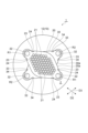
- FIG. FIG. 13 is a plan view of a discharge tube according to a first modified example.
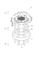
- FIG. 11 is a perspective view of a discharge tube according to a second modified example.
- the discharge tube 1 includes a container 10, an anode section 20, a cathode section 30, a pair of anode electrode sections 40, and a pair of cathode electrode sections 50.
- the anode section 20 and the cathode section 30 are arranged in the container 10 so as to face each other.
- direction D1 facing direction
- one side S1 upper side in FIG.
- the discharge tube 1 is a sensor that detects ultraviolet rays by utilizing the characteristics due to the work function of the cathode section 30.
- the discharge tube 1 is used for applications such as flame detection, combustion monitoring, discharge detection, and safety devices during hydrogen or ammonia combustion.
- the vessel 10 has a stem 11 and a glass bulb 12.
- the stem 11 is formed, for example, in the shape of a circular ring plate.
- An exhaust pipe 13 is connected to the center of the stem 11.
- the glass bulb 12 is formed, for example, in a substantially cylindrical shape with an end (top) on one side S1 in the direction D1 closed, and an end (bottom) on the other side S2 in the direction D1 joined to the outer edge of the stem 11. This makes the vessel 10 airtightly sealed.
- a discharge gas 2 is sealed in the vessel 10.
- the glass bulb 12 is formed, for example, from a material having ultraviolet light transparency. Examples of materials for the glass bulb 12 include borosilicate glass, ultraviolet light transmitting glass, quartz glass, and crystalline materials such as MgF2 .
- the anode portion 20 is formed in a flat plate shape from a metal material.
- the anode portion 20 is formed, for example, in a substantially diamond shape when viewed from direction D1.
- the anode portion 20 is formed in a substantially diamond shape with one diagonal longer than the other diagonal, and the longer diagonal is along direction D2 in which the pair of anode electrode portions 40 face each other.
- Each corner of the anode portion 20 in a plan view is curved so as not to have a sharp top.
- the anode portion 20 is formed, for example, from tungsten, nickel, molybdenum, copper, stainless steel, Kovar metal, etc.
- a plurality of openings 21 are formed that penetrate the anode part 20 along the direction D1.
- Each opening 21 is formed, for example, in a hexagonal shape.
- the multiple openings 21 are regularly arranged in a two-dimensional array at regular intervals.
- the anode part 20 has, in its center, a roughly diamond-shaped mesh part formed by the multiple openings 21 provided along the outer edge part 20a of the anode part 20, and the outer edge part has a frame part that surrounds the mesh part.
- the shape of the openings 21 may be a polygon other than a hexagon or a circle, and the arrangement, size, number, etc. of the openings 21 may be selected from various forms depending on the application.
- a recess 22 is formed at each end of the anode part 20 in the direction D2.
- the recess 22 opens to one side S1 in the direction D1 and is formed in a circular shape when viewed from the direction D1.
- the recess 22 is formed, for example, by half-etching, and is formed thinner than the part of the anode part 20 surrounding the recess 22.
- the plate material constituting the anode part 20 has a uniform thickness, so the recess 22 is formed thinner than the part of the anode part 20 other than the recess 22 (excluding the opening 21).
- the anode part 20 is joined to the anode electrode part 40 at the position of the recess 22 on the other side S2 in the direction D1.
- the recess 22 constitutes the joining region R1 with the anode electrode part 40.
- the outer edge 20a of the anode 20 has a plurality of notches 23 (four in this example).
- the notches 23 are formed as bridges connecting the metal member surrounding the anode 20 to the anode 20 when the anode 20 is formed, for example, by etching a plate-shaped metal member in the manufacturing process of the anode 20.
- the notches 23 are a necessary configuration for manufacturing, and do not have any function as an electrode.
- no bridges remain in the anode 20.
- the two notches 23 are arranged so as to face each other on both sides of one recess 22 in a direction perpendicular to the direction D2 when viewed from the direction D1.
- the remaining two notches 23 are arranged so as to face each other on both sides of the other recess 22 in a direction perpendicular to the direction D2 when viewed from the direction D1.
- Each notch 23 is formed, for example, in a semicircular shape when viewed from the direction D1.
- the cathode portion 30 is formed in a flat plate shape from a metal material.
- the cathode portion 30 has the same shape as the anode portion 20. That is, the cathode portion 30 is formed in a generally rhombus shape when viewed from direction D1.
- the cathode portion 30 is formed in a generally rhombus shape with one diagonal longer than the other diagonal, and the longer diagonal is along direction D3 in which the pair of cathode electrode portions 50 face each other.
- Each corner of the cathode portion 30 in a plan view is curved so as not to have a sharp top.
- the cathode portion 30 is formed from, for example, tungsten, nickel, molybdenum, copper, Kovar metal, etc.
- the cathode section 30 does not have an opening.
- light that passes through the opening 21 of the anode section 20 is incident on the surface 30b of the cathode section 30.
- the surface 30b is the surface (flat surface) of one side S1 in the direction D1 of the cathode section 30, and functions as a photocathode.
- the surface 30b emits photoelectrons in response to the incidence of light that has passed through the opening 21.
- a recess 32 is formed at each end of the cathode section 30 in the direction D3.
- the recess 32 opens to one side S1 in the direction D1 and is formed in a circular shape when viewed from the direction D1.
- the recess 32 is formed, for example, by half etching, and is formed thinner than the part of the cathode section 30 surrounding the recess 32.
- the plate material constituting the cathode section 30 has a uniform thickness, so the recess 32 is formed thinner than the part of the cathode section 30 other than the recess 32.
- the cathode section 30 is joined to the cathode electrode section 50 at the position of the recess 32 on the other side S2 in the direction D1.
- the recess 32 constitutes a joining region R2 with the cathode electrode section 50.
- the outer edge 30a of the cathode section 30 has multiple (four in this example) notches 33 formed therein.
- the notches 33 have the same configuration as the notches 23, and therefore a description thereof will be omitted here.
- the two notches 33 are arranged to face each other on both sides of one recess 32 in a direction perpendicular to direction D2.
- the remaining two notches 33 are arranged to face each other on both sides of the other recess 32 in a direction perpendicular to direction D2.
- Each notch 33 is formed, for example, in a semicircular shape when viewed from direction D1.
- the anode electrode portion 40 is a rod-shaped electrode pin (stem pin) that is arranged to penetrate the stem 11 and is fixed to the stem 11.
- the anode electrode portion 40 extends straight from the stem 11 along direction D1. When viewed from direction D1, the pair of anode electrode portions 40 are arranged to face each other in direction D2, sandwiching the center of the stem 11 therebetween.
- the anode electrode portion 40 is formed, for example, from Kovar metal.
- the anode electrode portion 40 is joined to the joining region R1 of the anode portion 20 at an end portion 40a on one side S1 in the direction D1, and extends from the anode portion 20 to the other side S2 in the direction D1. More specifically, the end portion 40a is joined to a portion of the surface 20b of the other side S2 in the direction D1 of the anode portion 20 that overlaps with the recess 22 in the direction D1. In this example, the anode electrode portion 40 is joined to the anode portion 20 by laser welding.
- the anode electrode part 40 When welding, for example, with the end 40a in contact with the anode part 20 on the other side S2 of the recess 22, laser light is irradiated onto the recess 22 from one side S1 in the direction D1, melting and solidifying at least one of the anode part 20 and the anode electrode part 40 in the recess 22, thereby joining the anode part 20 to the anode electrode part 40.
- the heights of the pair of anode electrode parts 40 are the same, and the anode part 20 is held perpendicular to the direction D1 by the pair of anode electrode parts 40. That is, the anode electrode part 40 also functions as a holding member that holds the anode part 20.
- the cathode electrode portion 50 is a rod-shaped electrode pin (stem pin) that is arranged to penetrate the stem 11 and is fixed to the stem 11.
- the cathode electrode portion 50 extends straight from the stem 11 along direction D1. When viewed from direction D1, the pair of cathode electrode portions 50 are arranged to face each other in direction D3, sandwiching the center of the stem 11 therebetween.
- the cathode electrode portion 50 is formed, for example, from Kovar metal.
- the cathode electrode portion 50 is joined to the joining region R2 of the cathode portion 30 at an end 50a on one side S1 in the direction D1, and extends from the cathode portion 30 to the other side S2 in the direction D1. More specifically, the end 50a is joined to a portion of the surface 30c of the other side S2 in the direction D1 of the cathode portion 30 that overlaps with the recess 32 in the direction D1. In this example, the cathode electrode portion 50 is joined to the cathode portion 30 by laser welding.
- the cathode electrode part 50 also functions as a holding member that holds the cathode part 30.
- the anode part 20 is located on one side S1 in the direction D1 with respect to the cathode part 30. Therefore, the height of the pair of anode electrode parts 40 is set higher than the height of the pair of cathode electrode parts 50.
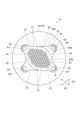
- the joint region R2 of the cathode portion 30 with the cathode electrode portion 50 is exposed from the anode portion 20 when viewed from one side S1 in the direction D1. That is, the anode portion 20 is not disposed on one side S1 of the joint region R2, and the joint region R2 does not overlap with the anode portion 20 in the direction D1. Also, when viewed from one side S1 in the direction D1, the notch portion 23 of the anode portion 20 is exposed from the cathode portion 30, and the notch portion 33 of the cathode portion 30 is exposed from the anode portion 20.
- a voltage is applied between the anode section 20 and the cathode section 30 via the anode electrode section 40 and the cathode electrode section 50.
- a use state when ultraviolet light is incident on the cathode section 30 (surface 30b) through the container 10 (glass bulb 12) and the opening 21 of the anode section 20, photoelectrons are emitted from the cathode section 30. These photoelectrons are attracted to the anode section 20 and collide with discharge gas molecules in the container 10 to ionize the discharge gas molecules.
- the electrons and positive ions generated by the ionization the electrons further collide with other discharge gas molecules and ionize them repeatedly to reach the anode section 20.
- the positive ions are accelerated toward the cathode section 30 and collide with the cathode section 30 to generate many secondary electrons.
- a current flows between the anode section 20 and the cathode section 30, and a discharge state is established. In the discharge tube 1, this discharge phenomenon is utilized to detect light in the ultraviolet region.
- the joining region R2 of the cathode portion 30 with the cathode electrode portion 50 is exposed from the anode portion 20 when viewed from one side S1 in the direction D1 (opposing direction). This makes both the joining region R2 of the cathode portion 30 with the cathode electrode portion 50 and the joining region R1 of the anode portion 20 with the anode electrode portion 40 visible from the one side S1 in the direction D1.
- laser light for laser welding can be irradiated from the one side S1 in the direction D1, thereby joining the cathode portion 30 to the cathode electrode portion 50 and joining the anode portion 20 to the anode electrode portion 40 in a single process.
- the manufacturing process can be simplified compared to the manufacturing method described in the above-mentioned Patent Document 1, in which the anode section 20 is positioned relative to the anode electrode section 40 after the cathode section 30 is joined to the cathode electrode section 50, and then the anode section 20 is joined to the anode electrode section 40.
- This makes it possible to reduce the number of steps in the manufacturing process, and to mass-produce the discharge tube 1.
- the joining region R2 of the cathode section 30 with the cathode electrode section 50 does not overlap with the anode section 20 in the direction D1, so that the occurrence of abnormal discharge caused by the joining region R2 overlapping with the anode section 20 can be suppressed.
- the manufacturing process of the discharge tube can be simplified and the detection accuracy can be improved.
- the anode section 20 and the cathode section 30 are made of flat plate-shaped members, so compared to, for example, a case in which the anode section and the cathode section have bent parts, the number of processes that may entail deformation of the members can be reduced, and the accuracy of the spacing between the anode section 20 and the cathode section 30 can be improved.
- the joining region R2 is formed thinner than the portion of the cathode section 30 surrounding the joining region R2. This makes it easier to join the cathode section 30 to the cathode electrode section 50.
- the joining region R2 is formed thinner than the portion of the cathode section 30 surrounding the joining region R2, so that laser welding can be performed using a laser beam with a lower output than when the joining region R2 is not formed thinner. This makes it easier to join the cathode section 30 to the cathode electrode section 50.
- the joining region R1 is formed thinner than the portion of the anode section 20 other than the joining region R1, so that it makes it easier to join the anode section 20 to the anode electrode section 40.
- the joining region R2 is formed thinner than the portion surrounding the joining region R2 by forming a recess 32 opening to one side S1 in the cathode portion 30.
- the recess 32 can be used as a marker, which can facilitate joining of the cathode portion 30 to the cathode electrode portion 50.
- the recess 32 serves as a marker for the welding location, so the welding location can be more easily identified than when there is no recess 32. Therefore, it is possible to facilitate joining of the cathode portion 30 to the cathode electrode portion 50.
- the joining region R2 is separated from the anode portion 20 in the direction D1 more than the portion other than the joining region R2. Therefore, even if the joining region R2 is deformed or the like due to joining, it is possible to prevent the distance from the anode portion 20 from becoming smaller in the direction D1. This reduces the possibility of discharge due to the bonding region R2.
- the bonding region R1 is formed thinner than the other portions of the anode section 20 by forming a recess 22 that opens to one side S1 in the anode section 20. In this case, the recess 22 can be used as a marker, making it easier to bond the anode section 20 to the anode electrode section 40.
- the cathode section 30 has a notch 33 formed in the outer edge section 30a, and the notch 33 is exposed from the anode section 20 when viewed from one side S1 in the direction D1. This makes it possible to suppress the occurrence of abnormal discharge caused by the notch 33 overlapping with the anode section 20. That is, when the notch 33 overlaps with the anode section 20, abnormal discharge may occur between the notch 33 and the anode section 20, but the cathode section 30 in this embodiment makes it possible to suppress the occurrence of such abnormal discharge.
- the anode section 20 has a notch 23 formed in the outer edge section 20a, and the notch 23 is exposed from the cathode section 30 when viewed from the other side S2 in the direction D1. This makes it possible to suppress the occurrence of abnormal discharge caused by the notch 23 overlapping with the cathode section 30. [Modification]
- the anode portion 20 has a protrusion 24 that protrudes from the inner surface of the cutout portion 23.
- the protrusion 24 is a burr that is generated, for example, when the anode portion 20 is separated from a metal member during the manufacturing process of the anode portion 20, and is part of the above-mentioned bridge portion that remains in the anode portion 20.
- the protrusion 24 is located within the cutout portion 23.
- the protrusion 24 is located inside the outer edge portion 20a of the anode portion 20 (the outer edge when it is assumed that the cutout portion 23 is not formed).
- the cathode portion 30 also has a protrusion 34 that protrudes from the inner surface of the cutout portion 33.
- the protrusion 34 is a burr that is generated, for example, when the cathode portion 30 is separated from a metal member during the manufacturing process of the cathode portion 30, and is part of the bridge portion described above that remains on the cathode portion 30.
- the protrusion 34 is located within the cutout portion 33.
- the protrusion 34 is located inside the outer edge portion 30a of the cathode portion 30 (the outer edge when it is assumed that the cutout portion 33 is not formed).
- the protrusion 34 is located within the cutout 33 when viewed from direction D1. This makes it possible to suppress the occurrence of abnormal discharge caused by the protrusion 34 protruding from the cutout 33. In other words, if the protrusion 34 is not located within the cutout 33, abnormal discharge may occur between the protrusion 34 and the anode 20, but according to the first modified example, the occurrence of such abnormal discharge can be suppressed.
- the discharge tube 1 may be configured as a second modified example shown in FIG. 4.
- the glass bulb 12 is omitted.
- the anode section 20 and the cathode section 30 are formed in a substantially triangular shape when viewed from the direction D1.
- Three anode electrode sections 40 are joined to the anode section 20, and the anode section 20 has three joining regions R1.
- the anode section 20 also has six notches 23.
- three cathode electrode sections 50 are joined to the cathode section 30, and the cathode section 30 has three joining regions R2.
- the cathode section 30 also has six notches 33.
- the joining region R2 of the cathode section 30 with the cathode electrode section 50 is exposed from the anode section 20 when viewed from one side S1 in the direction A.
- the manufacturing process of the discharge tube can be simplified and the detection accuracy can be improved, as in the above embodiment.
- the cathode electrode unit 50 was joined to the surface 30c of the other side S2 of the cathode unit 30, but the cathode electrode unit 50 may be joined to the surface 30b of one side S1 of the cathode unit 30.
- the cathode electrode unit 50 may be arranged so as to penetrate the cathode unit 30, and the protruding portion from the cathode unit 30 may be joined to the surface 30b of one side S1 of the cathode unit 30.
- the cathode electrode unit 50 may be joined to either the surface 30b of one side S1 of the cathode unit 30 or the surface 30c of the other side S2.
- the cathode electrode unit 50 joined to the surface 30c of the other side S2 of the cathode unit 30 as in the above embodiment.
- the anode electrode unit 40 may be joined to the surface of one side S1 of the anode unit 20, and may be joined to either the surface of one side S1 or the surface 20b of the other side S2 of the anode unit 20.
- the cathode electrode unit 50 and the cathode unit 30, and the anode electrode unit 40 and the anode unit 20 may be connected by indirect joining using a joining material such as brazing material, without being limited to direct joining by welding or the like.
- the cathode portion 30 may not have a recess 32, and the cathode portion 30 may have the same thickness throughout.
- the anode portion 20 may not have a recess 22, and the anode portion 20 may have the same thickness throughout.
- the recess 32 of the cathode portion 30 may be formed so as to open to the other side S2.
- the recess 22 of the anode portion 20 may be formed so as to open to the other side S2.
- the cutout portion 33 of the cathode portion 30 may overlap with the anode portion 20 when viewed from one side S1 in the direction D1.
- the cathode portion 30 may not have a cutout portion 33.
- the anode portion 20 may not have a cutout portion 23.
- the protrusion 34 of the cathode portion 30 may have a portion located outside the cutout portion 33 when viewed from the direction D1.
- the protrusion 24 of the anode section 20 may have a portion that is located outside the cutout portion 33 when viewed from the direction D1.
- 1...discharge tube 10...container, 20...anode portion, 21...opening, 30...cathode portion, 30a...outer edge portion, 32...recess, 33...notch portion, 34...protrusion, 40...anode electrode portion, 50...cathode electrode portion, D1...direction (facing direction), R2...joint area.
Landscapes
- Physics & Mathematics (AREA)
- General Physics & Mathematics (AREA)
- Spectroscopy & Molecular Physics (AREA)
- Electron Tubes For Measurement (AREA)
- Photometry And Measurement Of Optical Pulse Characteristics (AREA)
Abstract
放電管は、容器と、開口部を有する板状のアノード部と、開口部を通過した光の入射に応じて光電子を放出する板状のカソード部と、アノード部とカソード部が向かい合う対向方向に沿って延在する棒状のアノード電極部と、対向方向に沿って延在する棒状のカソード電極部と、を備える。対向方向においてアノード部がカソード部に対して位置する側を一方側とし、一方側とは反対側を他方側とすると、アノード電極部はアノード部から他方側に延在しており、カソード電極部はカソード部から他方側に延在している。カソード部におけるカソード電極部との接合領域は、対向方向における一方側から見た場合に、アノード部から露出している。
Description
本開示は、放電管に関する。
特許文献1には、アノード部と、カソード部と、アノード部及びカソード部にそれぞれ接続された複数のリード線と、を備えた紫外線検出用の放電管が記載されている。特許文献1に記載の放電管の製造時には、カソード部をリード線に溶接した後に、カソード部とアノード部との間にスペーサが配置される。その後に、アノード部がリード線に溶接され、スペーサが取り除かれる。
上述したような放電管には、製造工程を簡易化することが求められる。また、意図しない放電(異常放電)の発生を抑制し、検出精度を高めることが併せて求められる。
そこで、本開示の一側面は、放電管の製造工程を簡易化することができると共に、検出精度を高めることができる放電管を提供する。
本開示の一側面に係る放電管は、[1]「放電ガスが封入された容器と、開口部が形成された板状部材からなり、前記容器内に配置されたアノード部と、板状部材からなり、前記アノード部と向かい合うように前記容器内に配置され、前記開口部を通過した光の入射に応じて光電子を放出するカソード部と、前記アノード部と前記カソード部とが向かい合う対向方向に沿って延在し、前記アノード部に接合された棒状のアノード電極部と、前記対向方向に沿って延在し、前記カソード部に接合された棒状のカソード電極部と、を備え、前記アノード部と前記カソード部が向かい合う対向方向において前記アノード部が前記カソード部に対して位置する側を一方側とし、前記一方側とは反対側を他方側とすると、前記アノード電極部は前記アノード部から前記他方側に延在しており、前記カソード電極部は前記カソード部から前記他方側に延在しており、前記カソード部における前記カソード電極部との接合領域は、前記対向方向における前記一方側から見た場合に、前記アノード部から露出している、放電管」である。
この放電管では、カソード部におけるカソード電極部との接合領域が、対向方向における一方側から見た場合に、アノード部から露出している。これにより、カソード部におけるカソード電極部との接合領域、及びアノード部におけるアノード電極部との接合領域の両方が、対向方向における一方側から視認可能となる。そのため、この放電管の製造時には、例えば、カソード部をカソード電極部に対して位置決めすると共にアノード部をアノード電極部に対して位置決めした後に、カソード電極部に対するカソード部の接合、及びアノード電極部に対するアノード部の接合を1つの工程で行うことができる。その結果、上述した特許文献1に記載の製造方法のように、カソード部をカソード電極部に接合した後にアノード部をアノード電極部に対して位置決めし、その後にアノード部をアノード電極部に接合する場合と比べて、製造工程を簡易化することができる。また、この放電管では、カソード部におけるカソード電極部との接合領域が対向方向においてアノード部と重ならないため、当該接合領域がアノード部と重なることに起因する異常放電の発生を抑制することができる。よって、この放電管によれば、放電管の製造工程を簡易化することができると共に、検出精度を高めることができる。
本開示の一側面に係る放電管は、[2]「前記接合領域は、前記カソード部における前記接合領域を包囲する部分よりも薄く形成されている、[1]に記載の放電管」であってもよい。この場合、カソード電極部に対するカソード部の接合を容易化することができる。
本開示の一側面に係る放電管は、[3]「前記接合領域は、前記一方側に開口する凹部がカソード部に形成されることにより、前記接合領域を包囲する前記部分よりも薄く形成されている、[2]に記載の放電管」であってもよい。この場合、例えば凹部を接合時の目印として用いることができ、カソード電極部に対するカソード部の接合を容易化することができる。
本開示の一側面に係る放電管は、[4]「前記カソード部は、外縁部に形成された切欠き部を有し、前記切欠き部は、前記対向方向における前記一方側から見た場合に、前記アノード部から露出している、[1]~[3]のいずれかに記載の放電管」であってもよい。この場合、当該切欠き部がアノード部と重なることに起因する異常放電の発生を抑制することができる。
本開示の一側面に係る放電管は、[5]「前記カソード部は、前記切欠き部の内面から突出した突出部を更に有し、前記突出部は、前記対向方向から見た場合に、前記切欠き部内に位置している、[4]に記載の放電管」であってもよい。この場合、当該突出部が切欠き部から突出することに起因する異常放電の発生を抑制することができる。
本開示の一側面によれば、放電管の製造工程を簡易化することができると共に、検出精度を高めることができる放電管を提供することができる。
以下、本開示の一実施形態について、図面を参照しつつ詳細に説明する。なお、以下の説明において、同一又は相当要素には同一符号を用い、重複する説明を省略する。
図1及び図2に示されるように、放電管1は、容器10と、アノード部20と、カソード部30と、一対のアノード電極部40と、一対のカソード電極部50と、を備えている。アノード部20及びカソード部30は、互いに向かい合うように容器10内に配置されている。以下、アノード部20とカソード部30とが向かい合う方向を方向D1(対向方向)とし、方向D1においてアノード部20がカソード部30に対して位置する側を一方側S1(図1中の上側)とし、方向D1においてカソード部30がアノード部20に対して位置する側を他方側S2(図1中の下側)とする。放電管1は、カソード部30の仕事関数による特性を利用して、紫外線の検出を行うセンサである。放電管1は、例えば炎検知、燃焼監視、放電検知、水素やアンモニア燃焼時の安全装置等の用途に用いられる。
容器10は、ステム11と、ガラスバルブ12と、を有している。ステム11は、例えば円環板状に形成されている。ステム11の中央部には排気管13が接続されている。ガラスバルブ12は、例えば、方向D1における一方側S1の端部(頂部)が閉じられた略円筒状に形成されており、方向D1における他方側S2の端部(底部)においてステム11の外縁部に接合されている。これにより、容器10内は気密に封止されている。容器10内には放電ガス2が封入されている。ガラスバルブ12は、例えば紫外線透過性を有する材料により形成されている。ガラスバルブ12の材料としては、例えば、ホウケイ酸ガラス、紫外線透過ガラス、石英ガラス、MgF2等の結晶系材料等が挙げられる。
アノード部20は、金属材料により平板状に形成されている。アノード部20は、例えば、方向D1から見た場合に略菱形状に形成されている。この例では、アノード部20は、一方の対角線が他方の対角線よりも長い略菱形状に形成されており、長い方の対角線が、一対のアノード電極部40が向かい合う方向D2に沿っている。平面視におけるアノード部20の各角部は、尖った頂部を有さないように湾曲している。アノード部20は、例えば、タングステン、ニッケル、モリブデン、銅、ステンレス、コバール金属等により形成されている。
アノード部20の中央部には、方向D1に沿ってアノード部20を貫通する複数の開口部21(貫通孔)が形成されている。各開口部21は、例えば六角形状に形成されている。複数の開口部21は、一定の間隔を空けて二次元状に規則的に並んで配置されている。換言すれば、アノード部20は、その中央部には、アノード部20の外縁部20aに沿って設けられた複数の開口部21によって形成された略菱形状のメッシュ部を備え、その外縁部には、当該メッシュ部を包囲するような枠部を備えている。なお、開口部21の形状は六角形状以外の多角形状や円形状でもよく、その配置やサイズ、数等も用途に応じて様々な形態を選択することができる。
方向D2におけるアノード部20の各端部には、凹部22が形成されている。この例では、凹部22は、方向D1における一方側S1に開口しており、方向D1から見た場合に円形状に形成されている。凹部22は、例えばハーフエッチング加工により形成されており、アノード部20における凹部22を包囲する部分よりも薄く形成されている。なお、本実施形態においては、アノード部20を構成する板材は、均一の厚さを有しているため、凹部22は、アノード部20における凹部22以外の部分(開口部21を除く)よりも薄く形成されている。後述するように、アノード部20は、凹部22の位置で、方向D1における他方側S2において、アノード電極部40に接合されている。すなわち、凹部22は、アノード電極部40との接合領域R1を構成している。
アノード部20の外縁部20aには、複数(この例では4つ)の切欠き部23が形成されている。切欠き部23は、アノード部20の製造工程において、例えば板状の金属部材にアノード部20をエッチング等で形成した際、アノード部20を包囲する金属部材とアノード部20とをつなぐブリッジ部が形成される部位である。つまり、切欠き部23は、製造のために必要な構成であり、電極としての何らかの機能を担っている構成ではない。そして本実施形態においては、ブリッジ部はアノード部20には残っていない。2つの切欠き部23は、方向D1から見た場合に、一方の凹部22に対して、方向D2に垂直な方向における両側に、互いに対向するように配置されている。残りの2つの切欠き部23は、方向D1から見た場合に、他方の凹部22に対して、方向D2に垂直な方向における両側に、互いに対向するように配置されている。各切欠き部23は、例えば、方向D1から見た場合に半円形状に形成されている。
カソード部30は、金属材料により平板状に形成されている。この例では、カソード部30は、アノード部20と同一の形状を有している。すなわち、カソード部30は、方向D1から見た場合に略菱形状に形成されている。カソード部30は、一方の対角線が他方の対角線よりも長い略菱形状に形成されており、長い方の対角線が、一対のカソード電極部50が向かい合う方向D3に沿っている。平面視におけるカソード部30の各角部は、尖った頂部を有さないように湾曲している。カソード部30は、例えば、タングステン、ニッケル、モリブデン、銅、コバール金属等により形成されている。
アノード部20とは異なり、カソード部30には開口部が形成されていない。放電管1では、アノード部20の開口部21を通過した光がカソード部30の表面30bに入射する。表面30bは、カソード部30の方向D1における一方側S1の表面(平坦面)であり、光電面として機能する。表面30bは、開口部21を通過した光の入射に応じて光電子を放出する。
方向D3におけるカソード部30の各端部には、凹部32が形成されている。この例では、凹部32は、方向D1における一方側S1に開口しており、方向D1から見た場合に円形状に形成されている。凹部32は、例えばハーフエッチング加工により形成されており、カソード部30における凹部32を包囲する部分よりも薄く形成されている。なお、本実施形態においては、カソード部30を構成する板材は、均一の厚さを有しているため、凹部32は、カソード部30における凹部32以外の部分よりも薄く形成されている。後述するように、カソード部30は、凹部32の位置で、方向D1における他方側S2において、カソード電極部50に接合されている。すなわち、凹部32は、カソード電極部50との接合領域R2を構成している。
カソード部30の外縁部30aには、複数(この例では4つ)の切欠き部33が形成されている。なお、切欠き部33は、切欠き部23と同様の構成であるため、ここでは説明を省略する。2つの切欠き部33は、方向D1から見た場合に、一方の凹部32に対して、方向D2に垂直な方向における両側に、互いに対向するように配置されている。残りの2つの切欠き部33は、方向D1から見た場合に、他方の凹部32に対して、方向D2に垂直な方向における両側に、互いに対向するように配置されている。各切欠き部33は、例えば、方向D1から見た場合に半円形状に形成されている。
アノード電極部40は、棒状の電極ピン(ステムピン)であり、ステム11を貫通するように設けられ、ステム11に固定されている。アノード電極部40は、ステム11から方向D1に沿って真っ直ぐに延在している。一対のアノード電極部40は、方向D1から見た場合に、ステム11の中央部を挟んで方向D2において向かい合うように配置されている。アノード電極部40は、例えばコバール金属により形成されている。
アノード電極部40は、方向D1における一方側S1の端部40aにおいてアノード部20の接合領域R1に接合されており、アノード部20から方向D1における他方側S2に延在している。より具体的には、端部40aは、アノード部20の方向D1における他方側S2の表面20bのうち、方向D1において凹部22と重なる部分に接合されている。この例では、アノード電極部40は、レーザ溶接によりアノード部20に接合されている。
溶接時には、例えば、端部40aを凹部22の他方側S2においてアノード部20に接触させた状態で方向D1における一方側S1から凹部22にレーザ光を照射し、凹部22においてアノード部20およびアノード電極部40の少なくとも一方を溶融及び固化させることにより、アノード部20をアノード電極部40に接合する。一対のアノード電極部40の高さは互いに同一であり、一対のアノード電極部40によってアノード部20は方向D1と垂直に保持されている。すなわち、アノード電極部40は、アノード部20を保持する保持部材としても機能する。
カソード電極部50は、棒状の電極ピン(ステムピン)であり、ステム11を貫通するように設けられ、ステム11に固定されている。カソード電極部50は、ステム11から方向D1に沿って真っ直ぐに延在している。一対のカソード電極部50は、方向D1から見た場合に、ステム11の中央部を挟んで方向D3において向かい合うように配置されている。カソード電極部50は、例えばコバール金属により形成されている。
カソード電極部50は、方向D1における一方側S1の端部50aにおいてカソード部30の接合領域R2に接合されており、カソード部30から方向D1における他方側S2に延在している。より具体的には、端部50aは、カソード部30の方向D1における他方側S2の表面30cのうち、方向D1において凹部32と重なる部分に接合されている。この例では、カソード電極部50は、レーザ溶接によりカソード部30に接合されている。
溶接時には、例えば、端部50aを凹部32の他方側S2においてカソード部30に接触させた状態で方向D1における一方側S1から凹部32にレーザ光を照射し、凹部32においてカソード部30およびカソード電極部50の少なくとも一方を溶融及び固化させることにより、カソード部30をカソード電極部50に接合する。一対のカソード電極部50の高さは互いに同一であり、一対のカソード電極部50によってカソード部30は方向D1と垂直に且つアノード部20と平行に保持されている。すなわち、カソード電極部50は、カソード部30を保持する保持部材としても機能する。なお、上述したとおり、アノード部20はカソード部30に対して方向D1における一方側S1に位置している。したがって、一対のアノード電極部40の高さは、一対のカソード電極部50の高さよりも高く設定されている。
放電管1では、カソード部30におけるカソード電極部50との接合領域R2が、方向D1における一方側S1から見た場合に、アノード部20から露出している。すなわち、接合領域R2の一方側S1にはアノード部20が配置されておらず、接合領域R2は方向D1においてアノード部20と重なっていない。また、方向D1における一方側S1から見た場合に、アノード部20の切欠き部23がカソード部30から露出しており、カソード部30の切欠き部33がアノード部20から露出している。
放電管1の動作について説明する。使用状態においては、アノード電極部40及びカソード電極部50を介してアノード部20とカソード部30との間に電圧が印加されている。使用状態において、容器10(ガラスバルブ12)及びアノード部20の開口部21を介してカソード部30(表面30b)に紫外光が入射すると、カソード部30から光電子が放出される。この光電子は、アノード部20に引き寄せられ、容器10内の放電ガス分子と衝突して放電ガス分子を電離させる。電離によって発生した電子及び正イオンのうち、電子は更に他の放電ガス分子と衝突及び電離を繰り返してアノード部20に至る。一方、正イオンは、カソード部30に向けて加速され、カソード部30に衝突して多くの二次電子を発生させる。以上の現象を繰り返すことにより、アノード部20とカソード部30との間に電流が流れ、放電状態となる。放電管1では、この放電現象を利用して紫外域の光を検出する。
[作用効果]
[作用効果]
放電管1では、カソード部30におけるカソード電極部50との接合領域R2が、方向D1(対向方向)における一方側S1から見た場合に、アノード部20から露出している。これにより、カソード部30におけるカソード電極部50との接合領域R2、及びアノード部20におけるアノード電極部40との接合領域R1の両方が、方向D1における一方側S1から視認可能となる。そのため、放電管1の製造時には、例えば、カソード部30をカソード電極部50に対して位置決めすると共にアノード部20をアノード電極部40に対して位置決めした後に、レーザ溶接のためのレーザ光を方向D1における一方側S1から照射することで、カソード電極部50に対するカソード部30の接合、及びアノード電極部40に対するアノード部20の接合を一工程で行うことができる。その結果、上述した特許文献1に記載の製造方法のように、カソード部30をカソード電極部50に接合した後にアノード部20をアノード電極部40に対して位置決めし、その後にアノード部20をアノード電極部40に接合する場合と比べて、製造工程を簡易化することができる。これにより、製造工程における工数を削減することができ、放電管1の量産化を可能とすることができる。また、放電管1では、カソード部30におけるカソード電極部50との接合領域R2が方向D1においてアノード部20と重ならないため、当該接合領域R2がアノード部20と重なることに起因する異常放電の発生を抑制することができる。よって、放電管1によれば、放電管の製造工程を簡易化することができると共に、検出精度を高めることができる。また、放電管1では、アノード部20及びカソード部30が平板状部材からなるため、例えばアノード部及びカソード部が折り曲げ部分を有する場合と比べて、部材の変形を伴う可能性のある工程を低減できるため、アノード部20とカソード部30との間の間隔の精度を高めることができる。
接合領域R2が、カソード部30における接合領域R2を包囲する部分よりも薄く形成されている。これにより、カソード電極部50に対するカソード部30の接合を容易化することができる。例えば、カソード電極部50に対するカソード部30の接合をレーザ溶接にて行う場合に、接合領域R2がカソード部30における接合領域R2を包囲する部分よりも薄く形成されていることで、薄く形成されていない場合に比べてより少ない出力のレーザ光を用いてレーザ溶接を行うことができる。よって、カソード電極部50に対するカソード部30の接合を容易化することができる。また、接合領域R1が、アノード部20における接合領域R1以外の部分よりも薄く形成されていることで、アノード電極部40に対するアノード部20の接合を容易化することができる。
接合領域R2が、一方側S1に開口する凹部32がカソード部30に形成されることにより、接合領域R2を包囲する部分よりも薄く形成されている。この場合、例えば凹部32を目印として用いることができ、カソード電極部50に対するカソード部30の接合を容易化することができる。例えば、カソード電極部50に対するカソード部30の接合をカソード部30の一方側S1からレーザ溶接にて行う場合、凹部32が溶接箇所の目印となるため、凹部32が無い場合に比べて容易に溶接箇所を特定することができる。よって、カソード電極部50に対するカソード部30の接合を容易化することができる。また、凹部32が一方側S1に開口するように形成されているため、接合領域R2は、方向D1において、接合領域R2以外の部分よりもアノード部20に対して離間している。よって、仮に接合によって接合領域R2に変形等が生じても、方向D1においてアノード部20との距離が小さくなることを抑制することができる。よって、接合領域R2に起因する放電の可能性を低減することができる。また、接合領域R1が、一方側S1に開口する凹部22がアノード部20に形成されることにより、接合領域R1以外の部分よりも薄く形成されている。この場合、凹部22を目印として用いることができ、アノード電極部40に対するアノード部20の接合を容易化することができる。
カソード部30が、外縁部30aに形成された切欠き部33を有し、切欠き部33が、方向D1における一方側S1から見た場合に、アノード部20から露出している。これにより、切欠き部33がアノード部20と重なることに起因する異常放電の発生を抑制することができる。すなわち、切欠き部33がアノード部20と重なる場合、切欠き部33とアノード部20の間で異常放電が発生する可能性があるが、本実施形態におけるカソード部30によれば、このような異常放電の発生を抑制することができる。また、アノード部20が、外縁部20aに形成された切欠き部23を有し、切欠き部23が、方向D1における他方側S2から見た場合に、カソード部30から露出している。これにより、切欠き部23がカソード部30と重なることに起因する異常放電の発生を抑制することができる。
[変形例]
[変形例]
図3に示される第1変形例では、アノード部20が、切欠き部23の内面から突出した突出部24を有している。突出部24は、例えばアノード部20の製造工程において金属部材からアノード部20を切り離す際に生じるバリであり、アノード部20に残存した、上述したブリッジ部の一部である。突出部24は、方向D1から見た場合に、切欠き部23内に位置している。すなわち、突出部24は、方向D1から見た場合に、アノード部20の外縁部20a(切欠き部23が形成されていないと仮定した場合の外縁)よりも内側に位置している。
また、カソード部30が、切欠き部33の内面から突出した突出部34を有している。突出部34は、例えばカソード部30の製造工程において金属部材からカソード部30を切り離す際に生じるバリであり、カソード部30に残存した、上述したブリッジ部の一部である。突出部34は、方向D1から見た場合に、切欠き部33内に位置している。すなわち、突出部34は、方向D1から見た場合に、カソード部30の外縁部30a(切欠き部33が形成されていないと仮定した場合の外縁)よりも内側に位置している。
第1変形例では、突出部34が、方向D1から見た場合に、切欠き部33内に位置している。これにより、突出部34が切欠き部33から突出することに起因する異常放電の発生を抑制することができる。すなわち、突出部34が切欠き部33内に位置していない場合、突出部34とアノード部20との間で異常放電が発生することがあるが、第1変形例によれば、そのような異常放電の発生を抑制することができる。
放電管1は、図4に示される第2変形例のように構成されてもよい。図4では、ガラスバルブ12が省略して示されている。第2変形例では、アノード部20及びカソード部30は、方向D1から見た場合に略三角形状に形成されている。アノード部20には3つのアノード電極部40が接合されており、アノード部20は、3つの接合領域R1を有している。また、アノード部20は、6つの切欠き部23を有している。同様に、カソード部30には3つのカソード電極部50が接合されており、カソード部30は、3つの接合領域R2を有している。また、カソード部30は、6つの切欠き部33を有している。第2変形例においても、カソード部30におけるカソード電極部50との接合領域R2は、方向Aにおける一方側S1から見た場合に、アノード部20から露出している。このような第2変形例によっても、上記実施形態と同様に、放電管の製造工程を簡易化することができると共に、検出精度を高めることができる。
本開示は、上記実施形態及び変形例に限られない。例えば、各構成の材料及び形状には、上述した材料及び形状に限らず、様々な材料及び形状を採用することができる。
上記実施形態ではカソード電極部50がカソード部30における他方側S2の表面30cに接合されていたが、カソード電極部50は、カソード部30における一方側S1の表面30bに接合されていてもよい。例えば、カソード電極部50がカソード部30を貫通するように配置され、カソード部30からの突出部分においてカソード部30における一方側S1の表面30bに接合されていてもよい。すなわち、カソード電極部50は、カソード部30の一方側S1の表面30b及び他方側S2の表面30cのいずれか一方に接合されていればよい。ただし、上記実施形態のようにカソード電極部50がカソード部30の他方側S2の表面30cに接合されているほうが、異常放電の抑制等の観点において好ましい。同様に、アノード電極部40は、アノード部20における一方側S1の表面に接合されていてもよく、アノード部20の一方側S1の表面及び他方側S2の表面20bのいずれか一方に接合されていればよい。また、カソード電極部50とカソード部30、及びアノード電極部40とアノード部20とは、溶接等による直接的な接合に限らず、例えばロウ材等の接合材を用いた間接的な接合によって接続されてもよい。
カソード部30に凹部32が形成されていなくてもよく、カソード部30は全体にわたって同一の厚さを有していてもよい。アノード部20に凹部22が形成されていなくてもよく、アノード部20は全体にわたって同一の厚さを有していてもよい。カソード部30の凹部32は、他方側S2に開口するように形成されていてもよい。アノード部20の凹部22は、他方側S2に開口するように形成されていてもよい。カソード部30の切欠き部33は、方向D1における一方側S1から見た場合に、アノード部20と重なっていてもよい。カソード部30に切欠き部33が形成されていなくてもよい。アノード部20に切欠き部23が形成されていなくてもよい。第1変形例において、カソード部30の突出部34は、方向D1から見た場合に切欠き部33の外側に位置する部分を有していてもよい。第1変形例において、アノード部20の突出部24は、方向D1から見た場合に切欠き部33の外側に位置する部分を有していてもよい。
1…放電管、10…容器、20…アノード部、21…開口部、30…カソード部、30a…外縁部、32…凹部、33…切欠き部、34…突出部、40…アノード電極部、50…カソード電極部、D1…方向(対向方向)、R2…接合領域。
Claims (5)
- 放電ガスが封入された容器と、
開口部が形成された板状部材からなり、前記容器内に配置されたアノード部と、
板状部材からなり、前記アノード部と向かい合うように前記容器内に配置され、前記開口部を通過した光の入射に応じて光電子を放出するカソード部と、
前記アノード部と前記カソード部とが向かい合う対向方向に沿って延在し、前記アノード部に接合された棒状のアノード電極部と、
前記対向方向に沿って延在し、前記カソード部に接合された棒状のカソード電極部と、を備え、
前記アノード部と前記カソード部が向かい合う対向方向において前記アノード部が前記カソード部に対して位置する側を一方側とし、前記一方側とは反対側を他方側とすると、前記アノード電極部は前記アノード部から前記他方側に延在しており、前記カソード電極部は前記カソード部から前記他方側に延在しており、
前記カソード部における前記カソード電極部との接合領域は、前記対向方向における前記一方側から見た場合に、前記アノード部から露出している、放電管。 - 前記接合領域は、前記カソード部における前記接合領域を包囲する部分よりも薄く形成されている、請求項1に記載の放電管。
- 前記接合領域は、前記一方側に開口する凹部がカソード部に形成されることにより、前記接合領域を包囲する前記部分よりも薄く形成されている、請求項2に記載の放電管。
- 前記カソード部は、外縁部に形成された切欠き部を有し、
前記切欠き部は、前記対向方向における前記一方側から見た場合に、前記アノード部から露出している、請求項1~3のいずれか一項に記載の放電管。 - 前記カソード部は、前記切欠き部の内面から突出した突出部を更に有し、
前記突出部は、前記対向方向から見た場合に、前記切欠き部内に位置している、請求項4に記載の放電管。
Priority Applications (3)
| Application Number | Priority Date | Filing Date | Title |
|---|---|---|---|
| CN202380097998.9A CN121079755A (zh) | 2023-05-10 | 2023-12-28 | 放电管 |
| DE112023006316.8T DE112023006316T5 (de) | 2023-05-10 | 2023-12-28 | Entladungsröhre |
| KR1020257033833A KR20260006560A (ko) | 2023-05-10 | 2023-12-28 | 방전관 |
Applications Claiming Priority (2)
| Application Number | Priority Date | Filing Date | Title |
|---|---|---|---|
| JP2023-078046 | 2023-05-10 | ||
| JP2023078046A JP2024162497A (ja) | 2023-05-10 | 2023-05-10 | 放電管 |
Publications (1)
| Publication Number | Publication Date |
|---|---|
| WO2024232123A1 true WO2024232123A1 (ja) | 2024-11-14 |
Family
ID=93430128
Family Applications (1)
| Application Number | Title | Priority Date | Filing Date |
|---|---|---|---|
| PCT/JP2023/047335 Ceased WO2024232123A1 (ja) | 2023-05-10 | 2023-12-28 | 放電管 |
Country Status (5)
| Country | Link |
|---|---|
| JP (1) | JP2024162497A (ja) |
| KR (1) | KR20260006560A (ja) |
| CN (1) | CN121079755A (ja) |
| DE (1) | DE112023006316T5 (ja) |
| WO (1) | WO2024232123A1 (ja) |
Citations (6)
| Publication number | Priority date | Publication date | Assignee | Title |
|---|---|---|---|---|
| JP2005195404A (ja) * | 2004-01-05 | 2005-07-21 | Hamamatsu Photonics Kk | 紫外線検出管 |
| US20070131869A1 (en) * | 2005-12-12 | 2007-06-14 | Honeywell International Inc. | Ultra violet light sensor |
| JP2011014323A (ja) * | 2009-06-30 | 2011-01-20 | Yamatake Corp | 放電管のガラス間接合方法及び放電管 |
| CN202259154U (zh) * | 2011-09-30 | 2012-05-30 | 安徽华东光电技术研究所 | 一种高灵敏度紫外光电管 |
| JP2012255730A (ja) * | 2011-06-09 | 2012-12-27 | Azbil Corp | 火炎センサ |
| JP2015115228A (ja) * | 2013-12-12 | 2015-06-22 | アズビル株式会社 | 紫外線放電管及びその製造方法 |
Family Cites Families (1)
| Publication number | Priority date | Publication date | Assignee | Title |
|---|---|---|---|---|
| JP2012207971A (ja) | 2011-03-29 | 2012-10-25 | Azbil Corp | 火炎センサ及びその製造方法 |
-
2023
- 2023-05-10 JP JP2023078046A patent/JP2024162497A/ja active Pending
- 2023-12-28 KR KR1020257033833A patent/KR20260006560A/ko active Pending
- 2023-12-28 DE DE112023006316.8T patent/DE112023006316T5/de active Pending
- 2023-12-28 WO PCT/JP2023/047335 patent/WO2024232123A1/ja not_active Ceased
- 2023-12-28 CN CN202380097998.9A patent/CN121079755A/zh active Pending
Patent Citations (6)
| Publication number | Priority date | Publication date | Assignee | Title |
|---|---|---|---|---|
| JP2005195404A (ja) * | 2004-01-05 | 2005-07-21 | Hamamatsu Photonics Kk | 紫外線検出管 |
| US20070131869A1 (en) * | 2005-12-12 | 2007-06-14 | Honeywell International Inc. | Ultra violet light sensor |
| JP2011014323A (ja) * | 2009-06-30 | 2011-01-20 | Yamatake Corp | 放電管のガラス間接合方法及び放電管 |
| JP2012255730A (ja) * | 2011-06-09 | 2012-12-27 | Azbil Corp | 火炎センサ |
| CN202259154U (zh) * | 2011-09-30 | 2012-05-30 | 安徽华东光电技术研究所 | 一种高灵敏度紫外光电管 |
| JP2015115228A (ja) * | 2013-12-12 | 2015-06-22 | アズビル株式会社 | 紫外線放電管及びその製造方法 |
Also Published As
| Publication number | Publication date |
|---|---|
| JP2024162497A (ja) | 2024-11-21 |
| CN121079755A (zh) | 2025-12-05 |
| DE112023006316T5 (de) | 2026-02-19 |
| KR20260006560A (ko) | 2026-01-13 |
Similar Documents
| Publication | Publication Date | Title |
|---|---|---|
| EP1045428B1 (en) | Gas discharge tube | |
| JP4237411B2 (ja) | ガス放電管 | |
| US12191623B2 (en) | Light emitting sealed body and light source device | |
| JP5439079B2 (ja) | 電子管 | |
| EP1304718B1 (en) | Photomultiplier tube and production method therefor | |
| USRE38234E1 (en) | Ultraviolet detector | |
| JP2024162497A (ja) | 放電管 | |
| JP3854669B2 (ja) | 紫外線検出管 | |
| JP6941525B2 (ja) | 電子管の製造方法 | |
| US11961725B2 (en) | Phototube | |
| US11894223B2 (en) | Photoelectric tube | |
| JP2012207971A (ja) | 火炎センサ及びその製造方法 | |
| JP3872419B2 (ja) | 光電陰極、電子管及び光電陰極の組立方法 | |
| JP6976122B2 (ja) | 電子管 | |
| EP4174909B1 (en) | Light emitting sealed body and light source | |
| US10515775B1 (en) | Electron tube | |
| US10535487B1 (en) | Manufacturing method of electron tube | |
| CN111739772B (zh) | 电子管的制造方法 | |
| CN102918624A (zh) | 电子倍增部以及包含其的光电倍增管 | |
| CN111696845B (zh) | 电子管 | |
| JPS61142636A (ja) | 電子銃構体 | |
| JP3626312B2 (ja) | 電子管 | |
| JP5912719B2 (ja) | 電子管の製造方法 | |
| JP3430533B2 (ja) | 陰極線管の陰極構造 | |
| JP3345777B2 (ja) | 2重管形蛍光ランプ |
Legal Events
| Date | Code | Title | Description |
|---|---|---|---|
| 121 | Ep: the epo has been informed by wipo that ep was designated in this application |
Ref document number: 23936671 Country of ref document: EP Kind code of ref document: A1 |
|
| WWE | Wipo information: entry into national phase |
Ref document number: 112023006316 Country of ref document: DE |
|
| WWP | Wipo information: published in national office |
Ref document number: 112023006316 Country of ref document: DE |