WO2024214573A1 - 伸縮性デバイス - Google Patents
伸縮性デバイス Download PDFInfo
- Publication number
- WO2024214573A1 WO2024214573A1 PCT/JP2024/013133 JP2024013133W WO2024214573A1 WO 2024214573 A1 WO2024214573 A1 WO 2024214573A1 JP 2024013133 W JP2024013133 W JP 2024013133W WO 2024214573 A1 WO2024214573 A1 WO 2024214573A1
- Authority
- WO
- WIPO (PCT)
- Prior art keywords
- stretchable
- wiring
- region
- elastic
- substrate
- Prior art date
- Legal status (The legal status is an assumption and is not a legal conclusion. Google has not performed a legal analysis and makes no representation as to the accuracy of the status listed.)
- Ceased
Links
Images


Classifications
-
- H—ELECTRICITY
- H05—ELECTRIC TECHNIQUES NOT OTHERWISE PROVIDED FOR
- H05K—PRINTED CIRCUITS; CASINGS OR CONSTRUCTIONAL DETAILS OF ELECTRIC APPARATUS; MANUFACTURE OF ASSEMBLAGES OF ELECTRICAL COMPONENTS
- H05K1/00—Printed circuits
- H05K1/02—Details
- H05K1/0277—Bendability or stretchability details
- H05K1/0283—Stretchable printed circuits
-
- H—ELECTRICITY
- H05—ELECTRIC TECHNIQUES NOT OTHERWISE PROVIDED FOR
- H05K—PRINTED CIRCUITS; CASINGS OR CONSTRUCTIONAL DETAILS OF ELECTRIC APPARATUS; MANUFACTURE OF ASSEMBLAGES OF ELECTRICAL COMPONENTS
- H05K1/00—Printed circuits
- H05K1/02—Details
-
- H—ELECTRICITY
- H05—ELECTRIC TECHNIQUES NOT OTHERWISE PROVIDED FOR
- H05K—PRINTED CIRCUITS; CASINGS OR CONSTRUCTIONAL DETAILS OF ELECTRIC APPARATUS; MANUFACTURE OF ASSEMBLAGES OF ELECTRICAL COMPONENTS
- H05K1/00—Printed circuits
- H05K1/02—Details
- H05K1/03—Use of materials for the substrate
-
- H—ELECTRICITY
- H05—ELECTRIC TECHNIQUES NOT OTHERWISE PROVIDED FOR
- H05K—PRINTED CIRCUITS; CASINGS OR CONSTRUCTIONAL DETAILS OF ELECTRIC APPARATUS; MANUFACTURE OF ASSEMBLAGES OF ELECTRICAL COMPONENTS
- H05K1/00—Printed circuits
- H05K1/02—Details
- H05K1/11—Printed elements for providing electric connections to or between printed circuits
- H05K1/115—Via connections; Lands around holes or via connections
-
- H—ELECTRICITY
- H05—ELECTRIC TECHNIQUES NOT OTHERWISE PROVIDED FOR
- H05K—PRINTED CIRCUITS; CASINGS OR CONSTRUCTIONAL DETAILS OF ELECTRIC APPARATUS; MANUFACTURE OF ASSEMBLAGES OF ELECTRICAL COMPONENTS
- H05K3/00—Apparatus or processes for manufacturing printed circuits
- H05K3/46—Manufacturing multilayer circuits
Definitions
- This disclosure relates to stretchable devices.
- Stretchable devices in which stretchable wiring is mounted on a stretchable substrate have been known for some time. These stretchable devices can be worn on the human body.
- At least one stretchable wiring is provided on each of two opposing main surfaces of a plurality of stretchable substrates.
- a plurality of stretchable substrates equipped with stretchable wiring are stacked and pressed together with an interlayer stretchable substrate so that at least a portion of the stretchable wiring provided on each main surface is in contact with each other.
- the stretchable wiring applied to a stretchable device is required to have a small thickness in order to obtain excellent stretchability.
- a stretchable device having a laminated structure as described above a low profile device is required from the viewpoint of stretchability and wearing comfort, and therefore it is desirable for the stretchable wiring to be thin.
- damage such as cracks and breaks are likely to occur in the stretchable wiring due to stress generated by the stretching of the stretchable device, and the reliability of the stretchable device may be reduced.
- the main objective of this disclosure is to provide a stretchable device that has better reliability even when it has a layered structure.
- the elastic wiring has two wiring main surfaces that face each other in the lamination direction of the elastic base material, In a cross-sectional view, at least one of the wiring main surfaces includes a first region and a second region, A stretchable device is provided, wherein the first region is a region in which a part of the wiring main surface is raised in the stacking direction more than the second region.
- the stretchable device according to one embodiment of the present disclosure has better reliability even when it has a layered structure.
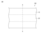
- FIG. 1 is a schematic plan view of a stretchable device according to a first embodiment of the present disclosure.
- FIG. 2 is a cross-sectional view of the stretchable device shown in FIG. 1 taken along line AA.
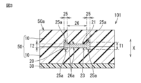
- FIG. 3 is a schematic cross-sectional view showing a stretchable device according to a modified example of the first embodiment of the present disclosure.
- FIG. 4A is a schematic plan view of a stretchable wiring according to various modified examples of the first embodiment of the present disclosure.
- FIG. 4B is a schematic plan view of the stretchable wiring according to various modified examples of the first embodiment of the present disclosure.
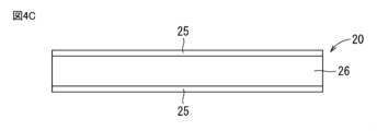
- FIG. 4C is a schematic plan view of a stretchable wiring according to various modified examples of the first embodiment of the present disclosure.
- FIG. 4D is a schematic plan view of a stretchable wiring according to various modified examples of the first embodiment of the present disclosure.
- FIG. 4E is a schematic plan view of a stretchable wiring according to various modified examples of the first embodiment of the present disclosure.
- FIG. 5 is a schematic plan view of a stretchable device according to a second embodiment of the present disclosure.
- FIG. 6 is a cross-sectional view of the stretchable device shown in FIG. 5 along line BB.
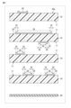
- FIG. 7 is a schematic cross-sectional view for explaining a method for producing a stretchable device according to the present disclosure.
- FIG. 8 is a schematic cross-sectional view for explaining a method for producing a stretchable device according to the present disclosure.
- FIG. 9A is a schematic cross-sectional view of a stretchable device used as an example.
- FIG. 9B is a schematic cross-sectional view of a stretchable device used as a comparative example.
- cross-sectional view or “cross-sectional shape” refers to the shape seen from a direction approximately perpendicular to the thickness direction of the stretchable device (in simple terms, the shape seen when cut along a plane parallel to the thickness direction of the stretchable device).
- the stretchable device has a layered structure comprising multiple stretchable substrates
- the "cross-sectional view” or “cross-sectional shape” refers to the shape seen from a direction approximately perpendicular to the layering direction of the stretchable substrates (in simple terms, the shape seen when cut along a plane parallel to the layering direction).
- planar view used in this specification refers to a sketch of the object as seen from above or below along the thickness direction (or layering direction) of the stretchable device.
- an element includes not only the case of contacting the top surface of the element, but also the case of not contacting the top surface of the element.
- an element does not only mean above, away from the element, i.e., above the element via another object or above with a gap, but also includes a position directly above the element.
- on does not necessarily mean above in the vertical direction. “On” merely indicates the relative positional relationship of an element.
- Figure 1 is a top view that shows a schematic diagram of a stretchable device 100 according to a first embodiment of the present disclosure.
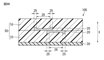
- Figure 2 is an A-A cross-sectional view of the stretchable device 100 in Figure 1.
- the cross-sectional views in this specification are cross-sections parallel to the thickness direction X of the stretchable device 100. In other words, they are cross-sections perpendicular to the stretching direction of the stretchable wiring 20. Even in the case of actual comparison, it can be confirmed by the above cross-sectional view at any position of the stretchable wiring 20 stretched in a certain direction.
- the stretchable wiring 20 is routed on the main surface 11 of the stretchable substrate 10.
- the shape of the stretchable device 100 is not particularly limited. In FIG. 1, for the sake of clarity, only wiring extending in a specific direction is shown, but the stretchable wiring 20 may extend in any direction on the main surface 11 of the stretchable substrate.
- the stretchable wiring 20 When viewed from the thickness direction X of the stretchable substrate 10, the stretchable wiring 20 does not necessarily have to be arranged in a straight line, and may be arranged in a curved line, for example. When viewed from the thickness direction X, the stretchable wiring does not necessarily have to extend in one direction.
- the number of stretchable wirings is also not particularly limited, and one or more wirings may be arranged.
- the stretchable device 100 may mainly include a stretchable substrate 10 and a stretchable wiring 20 provided on the main surface of the stretchable substrate 10.
- the stretchable device 100 may further include an adhesive layer 30 that can be attached to an adherend and contributes to the implementation of the stretchable device 100.
- adherend in this specification means the object to which the stretchable device is attached, and can also be called an adherend, an attached object, an object to be mounted, etc.
- adherend can be a living body.
- an elastic wiring 20 is provided on the main surface 11 of the elastic substrate, and an adhesive layer 30 is provided on the second main surface 12 side.
- the elastic substrate 10 (hereinafter, also simply referred to as “substrate”) is a sheet-like or film-like stretchable substrate, and is made of, for example, a resin material having elasticity.
- elasticity simply means the property of being able to expand and contract, and can also be called stretchability, stretchable, etc. More specifically, it means the property of being able to expand from a non-stretched state, which is the normal state in which no tensile stress is applied, by applying tensile stress, and being able to contract when released from the stretched state.
- resin materials used as the stretchable substrate include thermoplastic polyurethane.
- the elastic substrates 10 are stacked on top of each other in the thickness direction. More specifically, multiple elastic substrates 10 may have a multi-layer structure in which the multiple elastic substrates 10 are stacked with their main surfaces facing each other. In other words, multiple elastic substrates 10 may be stacked in the thickness direction X of the elastic substrate to form a laminate 50.
- the multiple elastic substrates 10 included in the laminate 50 may be made of the same material, or elastic substrates 10 made of different materials may be laminated.
- the elastic substrate located in the outermost layer of the laminate 50 e.g., the elastic substrate located most distal to the adhesive layer 30
- the elastic substrate located most distal to the adhesive layer 30 also contributes to protecting the elastic wiring 20 arranged inside the laminate 50, and can also be considered as a laminate layer, cover layer, protective layer, or coating layer.
- the thickness of the stretchable substrate 10 is not particularly limited, but in order to emphasize that the stretching of the surface of the adherend 200 is not hindered when the substrate is attached to an adherend such as a living body, the thickness is preferably 1 mm or less, more preferably 100 ⁇ m or less, and even more preferably 50 ⁇ m or less.
- the thickness of the stretchable substrate is preferably 1 ⁇ m or more.
- the multiple stretchable substrates 10 included in the laminate 50 do not necessarily have to be of the same thickness. In other words, the multiple stretchable substrates 10 may each be of a different thickness, and for example, only the outermost layer may be of a different thickness.
- the elastic wiring 20 (hereinafter also simply referred to as "wiring") contains conductive particles and resin.
- Examples of the elastic wiring 20 include a mixture of metal powder such as Ag (silver), Cu (copper), Ni (nickel) as conductive particles and an elastomer resin such as silicone resin.
- the average particle size of the conductive particles is not particularly limited, but is preferably 0.01 ⁇ m or more and 10 ⁇ m or less.
- the shape of the conductive particles is preferably spherical.
- the stretchable wiring 20 when the stretchable device has a multi-layer structure including a laminate 50 formed by stacking a plurality of stretchable substrates 10, the stretchable wiring 20 may be disposed inside the laminate 50. More specifically, the stretchable wiring 20 may be positioned on the main surface of the stretchable substrate 10, and the stretchable substrates 10 may be stacked together such that the stretchable wiring 20 is located inside the laminate 50. In other words, the plurality of stretchable substrates 10 may be stacked with the stretchable wiring 20 sandwiched between them.
- Such a structure can also be interpreted as the plurality of stretchable substrates 10 being stacked so that the stretchable wiring 20 disposed on the main surface of one of the stretchable substrates 10 is sandwiched between the other stretchable substrates 10.
- the stretchable wiring may be sandwiched between the stacked stretchable substrates 10 inside the laminate 50 formed by stacking a plurality of the stretchable substrates 10.
- the adhesive layer 30 has an adhesiveness that allows the stretchable device 100 to be attached to an adherend.
- the adhesive layer 30 has a substrate-side main surface located on the stretchable substrate 10 side and an adherend-side main surface located on the adherend side.
- the substrate-side main surface is a main surface located on the inside of the stretchable device 100, and the adherend-side main surface is located opposite to the substrate-side main surface and can be interpreted as a main surface located on the outside of the stretchable device 100.
- the stretchable device 100 is mounted so as to be bonded to the adherend on the adherend-side main surface of the adhesive layer 30, and the adherend-side main surface can also be referred to as an attachment surface, a sticking surface, or a mounting surface.
- the adhesive layer 30 has adhesiveness on both main surfaces. That is, the adhesive layer 30 may have adhesiveness not only on the attachment surface to the adherend but also on the substrate-side main surface.
- the adhesive layer can be attached to the adherend on the main surface located opposite the stretchable substrate.
- the adhesive layer 30 can be made of any adhesive that is low-irritation to the skin, has sufficient pressure-sensitive adhesiveness, and can be easily peeled off from the skin after use.
- examples of the adhesive layer 30 include synthetic rubber adhesives, acrylic adhesives, urethane adhesives, natural rubber adhesives, and/or silicone adhesives, with synthetic rubber adhesives being more preferred.
- the adhesive layer 30 has excellent stretchability and flexibility.
- the stretchable wiring 20 has a first wiring main surface 21 and a second wiring main surface 23, which are two wiring main surfaces facing each other in the stacking direction X of the stretchable substrate 10.
- the stacking direction X corresponds to the thickness direction of the stretchable substrate/stretchable wiring.
- the stretchable wiring 20 has a first region 25 (hereinafter also referred to as a raised region) in which at least one of the two wiring main surfaces is partially raised in the stacking direction X, and a second region 26 corresponding to the portion other than the first region 25.
- the first region 25 is a region in which a portion of the wiring main surface is raised in the stacking direction X more than the second region 26.
- the "first region (raised region)" refers to a region that protrudes in the stacking direction X at a different height in a cross-sectional view compared to a region other than the first region 25 of the wiring principal surface (i.e., the second region 26).
- the elastic wiring 20 refers to a region that is locally raised in the stacking direction X of the elastic substrate 10 compared to the second region 26.
- at least one of the wiring principal surfaces of the elastic wiring 20 is not a uniform flat surface, but has a raised region 25 in which a part of the wiring principal surface is raised in the stacking direction X.
- a "part of the wiring principal surface” refers to a portion that is greater than 0% and less than 60% of the surface area of the wiring principal surface when viewed from the stacking direction.
- the second region 26 refers to the portion of the wiring main surface other than the partially raised first region 25, and can also be called a non-raised region, or a main region or base region of the wiring main surface.
- the second region 26 can be understood as a region that is recessed relatively to the raised first region 25, or a region with a relatively reduced thickness.
- the elastic wiring 20 may have two regions with different thicknesses in a cross-sectional view.
- the thickness direction coincides with the stacking direction.
- the thickness of the elastic wiring 20 can also be expressed as the distance between the first wiring main surface 21 and the second wiring main surface 23 of the elastic wiring 20.
- the thickness T1 of the elastic wiring in the first region 25 may be larger than the thickness T2 of the elastic wiring in the second region 26 (see FIG. 3).
- the elastic wiring 20 may have a thickness in the second region 26 that is smaller than that of the first region 25.
- the region in which the elastic wiring 20 is relatively thick in a cross-sectional view can be interpreted as the first region 25, and the other region that is relatively thin can be interpreted as the second region 26. Therefore, the first region 25 can be referred to as a thick region, and the second region 26 can be referred to as a thin region, etc.
- the first region 25 and the second region 26 may be continuous with each other.
- the main wiring surface may be formed by a step surface that spans the first region 25 and the second region 26.
- the first region 25 and the second region 26 may be considered to be adjacent to each other.
- the main wiring surface may be formed by the second region 26, which is a plane extending approximately perpendicular to the stacking direction X, and the first region 25, which is continuous with the second region 26 and protrudes in the stacking direction X relative to the second region 26.
- the strength of the stretchable wiring 20 can be improved by partially increasing the thickness of the stretchable wiring 20 by the raised region 25. This can suitably suppress the occurrence and/or extension of cracks in the stretchable wiring 20, and as a result, can suitably prevent breakage of the wiring 20. Therefore, the present disclosure can provide a highly reliable stretchable device that can more suitably prevent damage to the stretchable wiring 20 during use of the stretchable device.
- the inventors of the present application have found that a structure including the above-mentioned raised region is suitable for achieving both the stretchability of the stretchable device and the prevention of breakage.
- a structure including the above-mentioned raised region is suitable for achieving both the stretchability of the stretchable device and the prevention of breakage.
- it is conceivable to increase the thickness of the wiring but an increase in the thickness of the wiring can be a factor in reducing the fit and/or stretchability of the stretchable device.
- the thickness is increased locally in the raised region 25 without increasing the overall thickness of the stretchable wiring 20, so that it is possible to reduce the reduction in the fit and/or stretchability of the stretchable device. Therefore, the stretchable device of the present disclosure is capable of achieving suitable stretchability of the stretchable device while suppressing breakage.
- the adhesion between the stretchable substrate and the stretchable wiring, which are joined by pressure bonding may be relatively weak. Therefore, when stretching the stretchable device, there is a risk of delamination occurring between the stretchable substrate and the stretchable wiring, which are joined by pressure bonding.
- the contact area between the elastic substrate 10 and the elastic wiring 20 is increased compared to when the elastic wiring 20 has a uniform surface (e.g., a smooth flat surface or a curved surface).
- the elastic substrate 10 and the elastic wiring 20 can be bonded over a larger area, and peeling (so-called delamination) between the substrate 10 and the wiring 20, which are bonded closely to each other and layered, can be preferably suppressed.
- an anchor effect can be produced in the bonding between the stretchable wiring 20 and the stretchable substrate 10.
- This anchor effect allows the wiring 20 and the substrate 10 to adhere more favorably.
- the peel resistance between the wiring 20 and the substrate 10 is further improved, and a stretchable device that is more favorable in terms of reliability can be obtained.
- the elastic wiring 20 and the elastic substrate 10 in contact with the elastic wiring 20 are bonded over the entire main wiring surface. That is, the elastic wiring 20 may be bonded to the elastic substrate 10 in both the first region 25 and the second region 26. More specifically, it is preferable that the elastic wiring 20 and the elastic substrate 10 are in close contact with each other on both the raised surface 25a of the first region, where a portion of the main wiring surface is raised, and the surface 26a of the second region. This makes it possible to more suitably obtain an increase in the bonding area between the elastic substrate 10 and the elastic wiring 20, and the effect of improving adhesion due to the anchor effect.
- the stretchable wiring 20 of the stretchable device 100 of the present disclosure may be able to improve the strength of the wiring 20 while favorably maintaining the stretchability. Therefore, the structure of the stretchable wiring 20 described in this specification may be favorably adopted not only for the stretchable wiring 20 present inside the laminate 50, in which both main surfaces (21, 23) of the wiring 20 are covered by the stretchable substrate 10, but also for the stretchable wiring 20 provided on the outermost surface 50a of the laminate, in which one of the wiring main surfaces is not opposed to the stretchable substrate 10 (see FIG. 8). Similarly, even in a single-layered stretchable device, by adopting the structure of the stretchable wiring of the present disclosure, a more favorable stretchable device in terms of strength and stretchability may be provided.
- the first region 25, which is the raised region, and the second region 26, which is the other region may extend at different heights in the stacking direction X in a cross-sectional view.
- the first region 25 and the second region 26 may provide a step structure on the wiring main surface.
- the raised surface of the first region 25 may be located at a different height from the surface of the second region 26 in the stacking direction X, thereby providing a step structure by the first region 25 and the second region 26.
- the stretchable wiring 20 can engage with the stretchable substrate 10 in a biting manner. This biting allows the anchor effect to work more effectively in the joining of the stretchable substrate 10 and the stretchable wiring 20, and therefore the peel resistance between the substrate 10 and the wiring 20 can be improved.
- the thickness T1 of the elastic wiring in the first region may be, for example, 105% or more of the thickness T2 of the elastic wiring in the second region, preferably 110% or more, and more preferably 125% or more (see FIG. 6).
- the thickness T1 of the elastic wiring in the first region may be, for example, 200% or less of the thickness T2 of the elastic wiring in the second region, preferably 180% or less, and more preferably 150% or less.
- the thickness T1 of the elastic wiring in the first region may be, for example, 1 ⁇ m or more larger than the thickness T2 of the elastic wiring in the second region, preferably 4.5 ⁇ m or more larger, and more preferably 5 ⁇ m or more larger.
- the difference in thickness between the thickness T1 of the elastic wiring in the first region and the thickness T2 of the elastic wiring in the second region may be, for example, 20 ⁇ m or less, and preferably 10 ⁇ m or less.
- a more suitable elastic device can be provided in terms of reliability and stretchability.
- the multiple stretchable wirings 20 when multiple stretchable wirings 20 are provided inside the laminate 50 and have at least a portion that overlaps with each other when viewed from the stacking direction X, the multiple stretchable wirings 20 may be insulated from each other by disposing the stretchable substrate 10 between the wirings 20.
- the stretchable substrate 10 interposed between the multiple stretchable wirings 20 may function as an insulator.
- damage to the stretchable substrate 10 and the resulting insulation breakdown are more suitably suppressed even in a state in which the thickness of the stretchable substrate 10 is relatively reduced as the stretchable device elongates. This can provide a stretchable device that is more suitable in terms of connection reliability and durability.
- the thickness T3 of the stretchable substrate facing the first region 25 in cross section is not particularly limited as long as the interlayer insulation can be ensured by the stretchable substrate 10.
- the thickness T3 of the stretchable substrate is not particularly limited as long as the conductive members such as the stretchable wiring 20 and electrodes (not shown) stacked via the stretchable substrate 10 are prevented from contacting each other and are insulated from each other.
- the thickness of the stretchable substrate 10 may be reduced when stretched, and if the importance is placed on ensuring insulation when the stretchable device is stretched, the thickness T3 of the stretchable substrate may be 5 ⁇ m or more.
- the stretchable device may be inferior in terms of stretchability and adhesion to the adherend. If the importance is placed on the stretchability of the stretchable device and adhesion of the stretchable device to the adherend, the thickness T3 of the stretchable substrate facing the first region 25 may be, for example, 500 ⁇ m or less.
- the thickness T3 of the elastic substrate facing the wiring main surface having the raised region 25 is greater than the thickness T2 of the elastic substrate in the raised region 25.
- the thickness T2 of the elastic substrate in the raised region 25 is preferably smaller than the thickness T3 of the elastic substrate adjacent to the wiring main surface having the raised region 25.
- the elastic substrate 10 in the portion facing the first region 25, which is the raised region is more susceptible to stress from the elastic substrate 20 than the portion facing the second region 26, which is not raised. Therefore, in some cases, there is a risk that the elastic substrate 10 may be easily torn when the elastic device is repeatedly stretched. Therefore, by ensuring a sufficient thickness of the elastic substrate 10, the stress that the elastic substrate 10 may exert on the elastic substrate 10 by the elastic substrate 20 in the raised region 25 can be suitably alleviated. This makes it possible to more suitably suppress damage to the elastic substrate 10.
- the thickness T3 of the elastic substrate facing the first region 25 may be, for example, 110% or more, or 115% or more, and preferably 120% or more, of the thickness T2 of the elastic wiring in the first region 25.
- the thickness T3 of the elastic substrate may be, for example, 200% or less, or 180% or less, and preferably 150% or less, of the thickness T2 of the elastic wiring in the first region 25.
- the dimensions of the stretchable substrate 10 and the first region 25 and second region 26 of the stretchable wiring 20, such as their thickness, are measured by cutting the stretchable device along the thickness direction and analyzing the cross section. For example, measurements can be made using a three-dimensional measuring machine (e.g., Mitutoyo's QV series) or a microscope (e.g., Keyence's VHX series).
- a three-dimensional measuring machine e.g., Mitutoyo's QV series
- a microscope e.g., Keyence's VHX series
- the elastic wiring 20 may have a plurality of first regions 25. More specifically, two or more first regions 25 may be provided on one of the wiring main surfaces. Additionally or alternatively, as described below, at least one first region 25 may be provided on each of two wiring main surfaces that face each other in the stacking direction X.
- the plurality of first regions 25 do not necessarily have to protrude at the same height in a cross-sectional view, and may protrude at different heights from each other. Furthermore, the cross-sectional shapes may also be different from each other. When a plurality of first regions are provided and each has a different thickness, the thickness T1 of the thickest part is taken as the thickness of the first region.
- FIGS. 4A to 4E are plan views showing various modified examples of the stretchable wiring 20 included in the stretchable device of the first embodiment.
- the raised region 25 may be formed at any position on the main wiring surface of the stretchable wiring 20 that faces the main surface 11 of the stretchable substrate.
- the raised region 25 may be disposed so as to extend to the center of the stretchable wiring 20 (FIG. 4A).
- the main wiring surface in a cross-sectional view, may have a structure including a first region 25 and two second regions 26 on either side of the first region 25.
- the raised region 25 is located on the periphery of the stretchable wiring 20 when viewed from the stacking direction X of the stretchable substrate 10 ( Figures 4B to 4E).
- the raised region 25 may extend so as to be located at least on the periphery of the stretchable wiring 20.
- the main wiring surface may have a region in which a part including at least the periphery is raised.
- the stretchable wiring 20 has a wiring side surface (or wiring end surface) that connects between the first wiring main surface 21 and the second wiring main surface 23, the raised region 25 may be provided so as to straddle the wiring side surface.
- the raised region 25 may be formed so as to be continuous with the wiring side surface.
- the "periphery of the elastic wiring” means the outer edge or outline of the elastic wiring 20 as viewed from the stacking direction X of the elastic substrate. Delamination between the elastic wiring 20 and the elastic substrate 10 and/or cracks in the elastic wiring 20 are likely to occur at the periphery of the elastic wiring 20. Therefore, by providing a raised region 25 at such a periphery and partially increasing the thickness of the elastic wiring 20, a more reliable elastic device in which the occurrence of breaks and delamination is suitably suppressed can be provided.
- the raised region 25 is provided so as to be located at least at the corner of the elastic wiring 20 (FIG. 4B).
- a corner means, for example, a portion where at least two sides that define the contour of the elastic wiring 20 are connected, and also includes a corner having a curved (for example, arc-shaped) shape.
- Such a corner is particularly likely to concentrate stress in the elastic wiring 20, and is likely to become the starting point for breakage and delamination of the elastic wiring 20. Therefore, by providing the raised region 25 at the corner of the elastic wiring 20, it may be possible to more suitably suppress the occurrence of breakage and delamination of the elastic wiring 20.
- the raised region 25 may extend along the periphery of the elastic wiring 20.
- the elastic wiring 20 may also have a plurality of raised regions 25 on one of the wiring main surfaces.
- the elastic wiring 20 may have two raised regions 25 extending along the periphery in the longitudinal direction of the elastic wiring 20 (FIG. 4C).
- the raised region 25 may extend along the periphery of the elastic wiring 20 so as to surround the wiring main surface of the elastic wiring 20 in a frame shape (FIGS. 4D and 4E). That is, as viewed from the stacking direction X, the elastic wiring 20 may have a raised region 25 formed in a frame shape along the contour of the elastic wiring 20.
- the elastic wiring 20 may have a first region 25 (i.e., a raised region) extending along the periphery of the elastic wiring 20 and a second region 26 surrounded by the first region 25.
- the stretchable wiring 20 may have a structure in which the peripheral portion is thick and the central portion is thin. This makes it possible to realize a more reliable stretchable device that can suppress breakage and/or delamination.
- the raised regions 25 may be formed intermittently as shown in FIG. 4D, or may be formed continuously as shown in FIG. 4E.
- the width dimension Wb of the raised region 25 in cross-sectional view is, for example, greater than 0% of the width dimension Wa of the elastic wiring, and preferably 10% or more (see Figure 4E).
- the width dimension Wb of the raised region 25 may be, for example, 30% or less of the width dimension Wa of the elastic wiring, and preferably 25% or less.
- the width dimension of the raised region 25 is in the above-mentioned range, a more reliable elastic device that can suitably suppress damage to the elastic device can be provided.
- the raised regions 25 may have different width dimensions from each other.
- the stretchable device 101 differs from the stretchable device 100 according to the first embodiment in that the stretchable wiring 20 includes raised regions 25 on each of two wiring main surfaces (21, 23) facing each other.
- Figure 3 is a schematic cross-sectional view of a stretchable device according to a modified example of the first embodiment.
- the stretchable wiring 20 may have a raised region 25 on each of the first wiring main surface 21 and the second wiring main surface 23 that face each other in the stacking direction X.
- the stretchable wiring 20 has at least two raised regions 25, one of which is located on the first wiring main surface 21 and the other of which is located on the second wiring main surface 23.
- the multiple raised regions 25 arranged on these different wiring main surfaces may be raised in different directions along the stacking direction X of the stretchable substrate 10.
- the raised region 25 can also be interpreted as being raised toward the stretchable substrate 10 that faces the wiring main surface on which the raised region 25 is located.
- the raised region 25 located on the first wiring main surface 21 may be raised upward along the stacking direction X
- the raised region 25 located on the second wiring main surface 23 may be raised downward along the stacking direction X.
- the raised regions 25 located on each wiring principal surface may be located coaxially along the stacking direction X. That is, it is preferable that the raised region 25 on the first wiring principal surface 21 and the raised region 25 on the second wiring principal surface 23 are located coaxially along the stacking direction X of the stretchable substrate. In other words, it is preferable that the raised region 25 on the first wiring principal surface 21 and the raised region 25 on the second wiring principal surface 23 overlap each other when viewed from the stacking direction X.
- the raised regions 25 are provided on each of the first wiring principal surface 21 and the second wiring principal surface 23 along the periphery of the elastic wiring 20. That is, in a cross-sectional view, the elastic wiring 20 may have raised regions 25 on each of the first wiring principal surface 21 and the second wiring principal surface 23 at both ends in the width direction. According to this structure, in a cross-sectional view, the elastic wiring 20 has a shape in which the thickness of both end portions of the elastic wiring 20 is greater than the thickness of the central portion (a shape including a so-called approximate dog-bone shape).
- the above-mentioned structure may be suitable not only for inhibiting the extension of cracks and the occurrence of breakage, but also for inhibiting delamination.
- the base region 26, which is the region other than the raised region 25, does not necessarily have to be flat.
- the base region 26 may be a curved surface.
- the raised region 25 may be formed by a part of the wiring main surface having the curved base region 26 being raised in the stacking direction X from the base region 26. Even in such a structure, the anchor effect is exerted by the raised region 25, and the effect of improving the adhesion between the wiring main surface and the stretchable substrate 10 that is joined opposite to the wiring main surface can be achieved.
- the stretchable device is different from the stretchable device 100 according to the first embodiment in that the laminate 50 includes a plurality of stretchable wires therein.
- FIG. 5 is a schematic plan view of a stretchable device 102 according to the second embodiment.
- FIG. 6 shows a cross-sectional view of the stretchable device 102 shown in FIG. 5 along line B-B.
- the stretchable device may include a plurality of stretchable wirings 20.
- the plurality of stretchable wirings 20 are arranged so as to be sandwiched between the substrates of a plurality of stretchable substrates 10 arranged in the stacking direction X, and may extend to different heights from each other as viewed from the stacking direction X.
- This structure can also be interpreted as a laminated structure in which two or more layers of stretchable substrates 10 each having at least one stretchable wiring 20 arranged on the main surface 11 are laminated.
- the plurality of stretchable wirings 20 may have at least a portion that overlaps with each other via the stretchable substrate 10 as viewed from the stacking direction X. In other words, it is preferable that the stretchable substrate 10 is interposed in the portion where the plurality of stretchable wirings 20 overlap as viewed from the stacking direction X. With this structure, multiple elastic wires 20 that overlap each other when viewed from the stacking direction X may be in non-contact with each other due to the presence of the elastic substrate 10.
- the multiple elastic wires 20 may overlap at the intersections when viewed from the stacking direction X.
- the multiple elastic wires 20 may extend approximately parallel to each other while overlapping each other when viewed from the stacking direction X.
- the elastic wiring 20 has a higher hardness than the elastic substrate 10.
- the inventors of the present application have found that when a plurality of elastic wirings 20 have portions in contact with each other in the stacking direction X between two adjacent elastic substrates 10, the contact portions of the wirings become locally hard, and stress distribution occurs, which may make the wirings 20 more likely to break. That is, when a plurality of elastic wirings 20 are stacked so as to be in contact with each other, stress tends to concentrate at the contact portions of the elastic wirings 20, and the wirings 20 may be more likely to be damaged.
- the contact portions of the elastic wirings 20 have a higher hardness than non-contact portions, so that the elongation rate of the elastic device may decrease overall.
- the elastic wirings 20 are indirectly overlapped with each other via the elastic substrate 10. This effectively reduces localized hardness variations, providing a stretchable device that is more resistant to breakage and more stretchable.
- multiple stretchable wirings 20 present between different layers may be conductively connected to each other through vias (not shown).
- stretchable wirings 20 located at different heights in the stacking direction X may be in non-contact with each other through the stretchable substrate 10, but may be electrically conductive through vias formed in the stretchable substrate 10.
- wiring and components e.g., electronic components such as electrodes or sensors located between different layers may be conductively connected to each other through vias.
- multiple stretchable wires 20 may be arranged between two adjacent stretchable substrates 10, as long as there is no direct contact between the stretchable wires 20 in the stacking direction X.
- multiple stretchable wires located between the same layers of two adjacently arranged stretchable substrates 10 when viewed from the stacking direction X may not have direct contact and may be arranged apart from each other (see FIG. 8).
- multiple stretchable wires 20 located between the same layers may be electrically connected by locally contacting each other. In other words, multiple stretchable wires 20 may be separated from each other, except for local contact for electrical conduction.
- a stretchable device includes multiple stretchable wirings 20, not all of the stretchable wirings 20 necessarily have a wiring main surface having the above-mentioned raised region 25.
- some of the stretchable wirings 20 may not have a raised region 25.
- the above-mentioned configuration is preferable in terms of delamination resistance between the stretchable substrate 10 and the stretchable wiring 20 located on the stretchable substrate 10, and may also be preferable in terms of peel resistance between the main wiring surface of the stretchable wiring 20 and any material that may be arranged opposite to the main wiring surface of the stretchable wiring 20.
- the stretchable wiring 20 having the structure of the present disclosure may be preferable in terms of peel resistance when bonded to other resin layers such as a resin cover layer or an adhesive layer that may be arranged on the main wiring surface.
- the stretchable device is different from the stretchable device 100 according to the first embodiment in that the stretchable wiring 20 has a wiring main surface with a predetermined surface roughness Ra.
- the surface roughness Ra of the wiring main surface having the above-mentioned raised region 25 is preferably 1.8 ⁇ m or more and less than 7.7 ⁇ m, 2 ⁇ m or more and less than 7.5 ⁇ m, or 2.3 ⁇ m or more and less than 7 ⁇ m.
- the elastic substrate 10 and the elastic wiring 20 can be more suitably bonded due to the anchor effect caused by the unevenness of the surface of the wiring main surface.
- the surface roughness of the first wiring principal surface 21 (see FIG. 2) and the surface roughness of the second wiring principal surface 23 do not necessarily have to be the same.
- both the first wiring principal surface 21 and the second wiring principal surface 23 of the elastic wiring 20 may have a surface roughness Ra in the above-mentioned range.
- the surface roughness Ra in both the first region 25 and the second region 26 is in the above-mentioned range. This allows the elastic wiring 20 to obtain an anchor effect due to the unevenness of the surface over the entire wiring principal surface. Therefore, even when the elastic device is stretched, the elastic substrate 10 and the elastic wiring 20 do not peel off, and can be deformed more suitably as one.
- surface roughness Ra means the arithmetic mean roughness in accordance with JIS B0601:2001.
- the surface roughness Ra of the main wiring surface is the arithmetic mean roughness measured on the cross section of the main wiring surface.
- the surface roughness Ra can be measured, for example, using a laser microscope.
- the stretchable substrate 10 is prepared.
- the stretchable wiring 20 is formed on the main surface 11 of the stretchable substrate 10 (see FIG. 7).
- the stretchable wiring 20 may be formed by printing a conductive paste (e.g., a conductive paste containing a mixture of silver and resin) onto the stretchable substrate 10 using screen printing, inkjet printing, or the like. This makes it possible to obtain a desired circuit pattern.
- the wiring pattern is formed so that a portion of the wiring is locally thickened, thereby forming a first region with a partially raised portion.
- the following two methods are exemplary formation methods.
- the first method is to allow a leveling time of about 5 seconds or more after printing the wiring, which allows the wiring to be formed with some parts (e.g., the periphery of the wiring) being thick and other parts (e.g., the central part of the wiring) being thin.
- the conductive paste for the stretchable wiring (e.g., a conductive paste containing a mixture of silver and resin) is printed on the stretchable substrate using screen printing and/or an inkjet method.
- the conductive paste for the stretchable wiring e.g., a conductive paste containing a mixture of silver and resin
- the elastic wiring 20 having the specified surface roughness Ra shown in the third embodiment can be obtained by controlling the mesh pattern in screen printing or the spray pattern of the conductive paste in inkjet printing when printing the wiring 20 on the elastic substrate 10.
- the conductive paste for stretchable wiring is dried and cured to form a stretchable wiring 20 whose thickness in a specified area is greater than the thickness of other areas. That is, a stretchable wiring 20 having a wiring main surface with a first area 25 and a second area 26 is formed on the stretchable substrate 10. Note that printing may be performed not only on one wiring main surface, but also on both the first wiring main surface and the second wiring main surface. It is also possible to mount components on the stretchable wiring as necessary.
- vias may be formed at predetermined positions on the stretchable substrate 10 that can contact each of the multiple stretchable wirings 20.
- the vias may be formed by providing through holes at predetermined positions on the stretchable substrate and filling the through holes with a conductive material (e.g., a conductive paste containing a mixture of silver and resin).
- the through holes can be formed, for example, by punching or laser processing.
- the planar shapes of the through holes and vias are not particularly limited and can be, for example, a perfect circle, an ellipse, or a polygon.
- the stretchable substrate 10 on which the desired circuit pattern has been printed is stacked in the thickness direction X of the stretchable substrate 10, and pressed at a desired temperature and pressure to obtain a laminated stretchable device (see Figures 7 and 8).
- a method for increasing the adhesion between the stretchable wiring 20 with the raised regions prepared earlier and the stretchable substrates located on both main surfaces thereof for example, the following methods are possible.
- the temperature of the elastic substrate 10 may be sufficiently raised to above the glass transition point of the resin used as the elastic substrate 10.
- the material of the elastic substrate 10 is a styrene-based elastomer
- it may be heated to a temperature of about 80°C.
- the heating temperature is a temperature below the softening point of the material of the elastic wiring 20.
- Samples Examples 1 to 6 and Comparative Examples 1 and 2 are samples formed by varying the thickness difference between the second region and the first region raised relative to the second region on the wiring main surface facing the stretchable substrate for the stretchable device described above.
- the planar shape of the wiring main surface in cross-sectional view is as shown in FIG. 1, and the cross-sectional shape is as shown in FIG. 3. That is, in this evaluation, a stretchable wiring was adopted that has a first region along the periphery of the wiring main surface on both sides of the wiring main surface in cross-sectional view, and a second region in the central portion surrounded by the first region.
- a composite paste of silver and acrylic resin was used as the material for the stretchable wiring.
- a stretchable wiring 2 mm wide and 90 mm long was printed on one of the stretchable substrates (styrene-based elastomer, 100 mm x 70 mm x 40 ⁇ m) using the screen printing method.
- the stretchable wiring was printed so that the thickness of the wiring increased in a 200 ⁇ m wide area along the periphery of the stretchable wiring.
- the stretchable substrate was then laminated and pressed at a specified pressure (1 MPa) to obtain a stretchable device.
- the stretchable device of Comparative Example 3 in which multiple stretchable wirings are arranged so as to directly overlap each other, and the stretchable device of Example 7, in which a stretchable substrate is interposed, had similar peel elongation rates.
- the stretchable device of Example 7 had a wire breakage elongation rate that was 1.4 times that of Comparative Example 3. Therefore, it was found that by interposing a stretchable substrate so that multiple stretchable wirings do not directly overlap each other in the stacking direction, the bias in the stress distribution at the overlapping portions of the stretchable wirings is suitably alleviated, and wire breakage during stretching of the stretchable device can be suitably suppressed.
- a stretchable device with high connection reliability that is more suitable in terms of wire breakage resistance during stretching of the stretchable device can be provided.
- the surface roughness Ra of the wiring principal surface was measured for each sample. Specifically, the stretchable device was cut along the lamination direction, and the cross section was observed using a laser microscope to measure the arithmetic average surface roughness Ra of the second region on the first wiring principal surface of the stretchable wiring. Furthermore, the peel elongation rate and the breakage elongation rate of the wiring were measured by a tensile test. The measurement results are shown in Table 3.
- the peel elongation rate improves as the surface roughness Ra of the wiring main surface increases.
- the rougher the wiring main surface the better the adhesion between the stretchable substrate and the stretchable wiring due to the anchor effect. Therefore, according to the present disclosure, a more reliable stretchable device can be provided that is more suitable in terms of peel resistance between the substrate/wiring when the stretchable device is stretched.
- the stretchable device of Comparative Example 6 which has a surface roughness Ra of 7.9 ⁇ m, showed a high peel elongation rate, but showed a low value for the fracture elongation rate of the wiring. This is thought to be because the strength of the wiring itself was reduced due to excessive roughening of the wiring main surface.
- First aspect A laminate formed by laminating a plurality of elastic base materials and an elastic wiring disposed inside the laminate,
- the elastic wiring has two wiring main surfaces that face each other in the lamination direction of the elastic base material,
- at least one of the wiring main surfaces includes a first region and a second region,
- the first region is a region in which a part of the wiring main surface is raised in the stacking direction more than the second region.
- Second aspect In the first aspect, in a cross-sectional view, the thickness of the elastic wire in the first region is greater than the thickness of the elastic wire in the second region.
- the first region is on the periphery of the stretchable wiring when viewed from the stacking direction.
- the first region is located at least at a corner of the elastic wiring when viewed from the stacking direction.
- the first region extends along a periphery of the elastic wiring when viewed from the stacking direction.
- each of the two wiring main surfaces has the first region, A stretchable device, in which, in a cross-sectional view, the first region on one of the wiring principal surfaces and the first region on the other of the wiring principal surfaces are raised in different directions from each other along the stacking direction of the stretchable substrate.
- a stretchable device In any one of the first to seventh aspects, the elastic wiring is engaged with the elastic substrate adjacent to the first region in the first region.
- the stretchable device, in a cross-sectional view, the second region is a non-raised region.
- a step structure is provided on the wiring main surface by the first region and the second region.
- the first region is in contact with adjacent stretchable substrates.
- the thickness of the elastic wiring in the first region is smaller than the thickness of the elastic substrate adjacent to the first region.
- the elastic wiring is provided in plurality, The plurality of elastic wirings are arranged between the plurality of elastic substrates arranged in the stacking direction, A stretchable device, wherein the plurality of stretchable wirings are positioned so that, when viewed from the stacking direction, they have at least a portion that overlaps with each other via the stretchable substrate.
- the elastic wiring is provided in plurality, The plurality of elastic wirings are arranged between the plurality of elastic substrates arranged in the stacking direction, The plurality of stretchable wires are arranged so as to be non-contact with each other in the stacking direction.
- the stretchable device further comprises the stretchable wiring on the outermost surface of the laminate.
- the thickness of the elastic wire in the first region is 5 ⁇ m or more greater than the thickness of the elastic wire in the second region.
- the surface roughness Ra of the wiring surface of the stretchable wiring is 2 ⁇ m or more and less than 7.5 ⁇ m.
- Stretchable device 10 Stretchable substrate 11: Main surface 20: Stretchable wiring 21: First wiring main surface 23: Second wiring main surface 25: First region (raised region) 25a: raised surface 26: second region 30: adhesive layer 50: laminate X: thickness direction of elastic substrate
Landscapes
- Engineering & Computer Science (AREA)
- Microelectronics & Electronic Packaging (AREA)
- Manufacturing & Machinery (AREA)
- Structure Of Printed Boards (AREA)
- Springs (AREA)
Priority Applications (3)
| Application Number | Priority Date | Filing Date | Title |
|---|---|---|---|
| JP2025513893A JP7786643B2 (ja) | 2023-04-11 | 2024-03-29 | 伸縮性デバイス |
| CN202480011930.9A CN120731663A (zh) | 2023-04-11 | 2024-03-29 | 伸缩性器件 |
| US19/283,611 US20250358930A1 (en) | 2023-04-11 | 2025-07-29 | Stretchable device |
Applications Claiming Priority (2)
| Application Number | Priority Date | Filing Date | Title |
|---|---|---|---|
| JP2023-064412 | 2023-04-11 | ||
| JP2023064412 | 2023-04-11 |
Related Child Applications (1)
| Application Number | Title | Priority Date | Filing Date |
|---|---|---|---|
| US19/283,611 Continuation US20250358930A1 (en) | 2023-04-11 | 2025-07-29 | Stretchable device |
Publications (1)
| Publication Number | Publication Date |
|---|---|
| WO2024214573A1 true WO2024214573A1 (ja) | 2024-10-17 |
Family
ID=93059315
Family Applications (1)
| Application Number | Title | Priority Date | Filing Date |
|---|---|---|---|
| PCT/JP2024/013133 Ceased WO2024214573A1 (ja) | 2023-04-11 | 2024-03-29 | 伸縮性デバイス |
Country Status (4)
| Country | Link |
|---|---|
| US (1) | US20250358930A1 (https=) |
| JP (1) | JP7786643B2 (https=) |
| CN (1) | CN120731663A (https=) |
| WO (1) | WO2024214573A1 (https=) |
Citations (5)
| Publication number | Priority date | Publication date | Assignee | Title |
|---|---|---|---|---|
| JP2010263470A (ja) * | 2009-05-08 | 2010-11-18 | Murata Mfg Co Ltd | 信号線路及びその製造方法 |
| JP2018018898A (ja) * | 2016-07-26 | 2018-02-01 | 富士通株式会社 | 配線基板及び電子機器 |
| WO2018123818A1 (ja) * | 2016-12-27 | 2018-07-05 | 日立化成株式会社 | 金属箔付伸縮性部材 |
| JP2019165049A (ja) * | 2018-03-19 | 2019-09-26 | 株式会社フジクラ | 伸縮性配線板 |
| CN113556879A (zh) * | 2020-04-23 | 2021-10-26 | 源秩科技(上海)有限公司 | 电路板制作方法及其线路层加工装置 |
Family Cites Families (9)
| Publication number | Priority date | Publication date | Assignee | Title |
|---|---|---|---|---|
| JPS6482595A (en) * | 1987-09-25 | 1989-03-28 | Meiko Electronics Co Ltd | Printed wiring board |
| JPH11274735A (ja) * | 1998-03-25 | 1999-10-08 | Toshiba Battery Co Ltd | 多層印刷配線板 |
| JP2006179589A (ja) * | 2004-12-21 | 2006-07-06 | Matsushita Electric Ind Co Ltd | 多層フレキシブル配線基板、その製造方法および多層フレキシブル配線の回路基板との接続方法 |
| EP3197250A4 (en) * | 2015-05-01 | 2018-01-17 | Fujikura Ltd. | Wiring body, wiring substrate, and touch sensor |
| JP6823472B2 (ja) * | 2016-02-22 | 2021-02-03 | 日本メクトロン株式会社 | 伸縮性配線基板及びその製造方法 |
| WO2019131581A1 (ja) * | 2017-12-26 | 2019-07-04 | 株式会社村田製作所 | インダクタブリッジおよび電子機器 |
| JP7001158B2 (ja) * | 2018-06-07 | 2022-01-19 | 株式会社村田製作所 | 多層基板、電子機器および多層基板の製造方法 |
| JP7279399B2 (ja) * | 2019-02-20 | 2023-05-23 | 大日本印刷株式会社 | 配線基板及び配線基板の製造方法 |
| JP7160180B2 (ja) * | 2019-03-20 | 2022-10-25 | 株式会社村田製作所 | 伝送路基板、および伝送路基板の実装構造 |
-
2024
- 2024-03-29 JP JP2025513893A patent/JP7786643B2/ja active Active
- 2024-03-29 CN CN202480011930.9A patent/CN120731663A/zh active Pending
- 2024-03-29 WO PCT/JP2024/013133 patent/WO2024214573A1/ja not_active Ceased
-
2025
- 2025-07-29 US US19/283,611 patent/US20250358930A1/en active Pending
Patent Citations (5)
| Publication number | Priority date | Publication date | Assignee | Title |
|---|---|---|---|---|
| JP2010263470A (ja) * | 2009-05-08 | 2010-11-18 | Murata Mfg Co Ltd | 信号線路及びその製造方法 |
| JP2018018898A (ja) * | 2016-07-26 | 2018-02-01 | 富士通株式会社 | 配線基板及び電子機器 |
| WO2018123818A1 (ja) * | 2016-12-27 | 2018-07-05 | 日立化成株式会社 | 金属箔付伸縮性部材 |
| JP2019165049A (ja) * | 2018-03-19 | 2019-09-26 | 株式会社フジクラ | 伸縮性配線板 |
| CN113556879A (zh) * | 2020-04-23 | 2021-10-26 | 源秩科技(上海)有限公司 | 电路板制作方法及其线路层加工装置 |
Also Published As
| Publication number | Publication date |
|---|---|
| CN120731663A (zh) | 2025-09-30 |
| US20250358930A1 (en) | 2025-11-20 |
| JPWO2024214573A1 (https=) | 2024-10-17 |
| JP7786643B2 (ja) | 2025-12-16 |
Similar Documents
| Publication | Publication Date | Title |
|---|---|---|
| JP7119406B2 (ja) | 伸縮性配線基板およびその製造方法 | |
| JP6405334B2 (ja) | 伸縮性配線基板、及び、伸縮性配線基板の製造方法 | |
| JP2017069530A (ja) | 伸縮性配線基板および伸縮性配線基板の製造方法 | |
| JP7252529B2 (ja) | 伸縮配線部材 | |
| JP6959226B2 (ja) | フレキシブルプリント配線板、接続体の製造方法及び接続体 | |
| TWI497535B (zh) | 具有軟性材料層之微電阻元件及其製造方法 | |
| JP5447735B2 (ja) | フレキシブル多層基板 | |
| US20230345635A1 (en) | Flexible printed circuit board, cof module, and electronic device comprising the same | |
| TW201633865A (zh) | 印刷配線板 | |
| CN100550519C (zh) | 柔软性良导电层、各向异性导电片及其制造方法 | |
| US20130120948A1 (en) | Circuit component and method of making the same | |
| JP7786643B2 (ja) | 伸縮性デバイス | |
| US7244127B2 (en) | Anisotropic conductive sheet and its manufacturing method | |
| JP2010287378A (ja) | 太陽電池セル接続用コネクタ及び太陽電池セルの接続方法 | |
| JP7718604B2 (ja) | 伸縮性デバイス | |
| JP2008252058A (ja) | 半導体装置及びその製造方法 | |
| TWI277190B (en) | Package structure for electronic device | |
| WO2023105873A1 (ja) | 伸縮デバイス | |
| JP3664171B2 (ja) | 半導体装置の製造方法及び半導体装置の製造装置 | |
| JP4030220B2 (ja) | 半導体チップの実装構造 | |
| WO2023184788A1 (zh) | 焊接方法、弹性电接触端子的焊接结构以及电子设备 | |
| WO2025033274A1 (ja) | 伸縮性デバイス | |
| WO2025249078A1 (ja) | 伸縮性デバイス | |
| WO2025192170A1 (ja) | 伸縮性デバイス | |
| JP7758216B2 (ja) | 伸縮性デバイス |
Legal Events
| Date | Code | Title | Description |
|---|---|---|---|
| 121 | Ep: the epo has been informed by wipo that ep was designated in this application |
Ref document number: 24788600 Country of ref document: EP Kind code of ref document: A1 |
|
| ENP | Entry into the national phase |
Ref document number: 2025513893 Country of ref document: JP Kind code of ref document: A |
|
| WWE | Wipo information: entry into national phase |
Ref document number: 2025513893 Country of ref document: JP |
|
| WWE | Wipo information: entry into national phase |
Ref document number: 202480011930.9 Country of ref document: CN |
|
| WWP | Wipo information: published in national office |
Ref document number: 202480011930.9 Country of ref document: CN |
|
| NENP | Non-entry into the national phase |
Ref country code: DE |
|
| 122 | Ep: pct application non-entry in european phase |
Ref document number: 24788600 Country of ref document: EP Kind code of ref document: A1 |