WO2024204600A1 - 撮像素子および撮像装置 - Google Patents
撮像素子および撮像装置 Download PDFInfo
- Publication number
- WO2024204600A1 WO2024204600A1 PCT/JP2024/012785 JP2024012785W WO2024204600A1 WO 2024204600 A1 WO2024204600 A1 WO 2024204600A1 JP 2024012785 W JP2024012785 W JP 2024012785W WO 2024204600 A1 WO2024204600 A1 WO 2024204600A1
- Authority
- WO
- WIPO (PCT)
- Prior art keywords
- signal processing
- output
- signal
- unit
- pixel
- Prior art date
- Legal status (The legal status is an assumption and is not a legal conclusion. Google has not performed a legal analysis and makes no representation as to the accuracy of the status listed.)
- Ceased
Links
Images






Classifications
-
- H—ELECTRICITY
- H04—ELECTRIC COMMUNICATION TECHNIQUE
- H04N—PICTORIAL COMMUNICATION, e.g. TELEVISION
- H04N23/00—Cameras or camera modules comprising electronic image sensors; Control thereof
- H04N23/60—Control of cameras or camera modules
- H04N23/63—Control of cameras or camera modules by using electronic viewfinders
-
- H—ELECTRICITY
- H04—ELECTRIC COMMUNICATION TECHNIQUE
- H04N—PICTORIAL COMMUNICATION, e.g. TELEVISION
- H04N23/00—Cameras or camera modules comprising electronic image sensors; Control thereof
- H04N23/60—Control of cameras or camera modules
- H04N23/667—Camera operation mode switching, e.g. between still and video, sport and normal or high- and low-resolution modes
-
- H—ELECTRICITY
- H04—ELECTRIC COMMUNICATION TECHNIQUE
- H04N—PICTORIAL COMMUNICATION, e.g. TELEVISION
- H04N25/00—Circuitry of solid-state image sensors [SSIS]; Control thereof
- H04N25/70—SSIS architectures; Circuits associated therewith
Definitions
- the present invention relates to an imaging element and an imaging apparatus.
- This application claims priority based on Japanese Patent Application No. 2023-051434, filed on March 28, 2023, the contents of which are incorporated herein by reference.
- Patent Document 1 Image sensors that simultaneously read out live view images and still images are known (for example, Patent Document 1).
- the conventional technology has a problem in that the display of the live view image is interrupted.
- an imaging element includes a plurality of pixels that output signals based on photoelectrically converted charges, a first signal processing unit having a first signal processing circuit that applies first signal processing to the signals output from the pixels to generate image data for display, a second signal processing unit having a second signal processing circuit that applies second signal processing to the signals output from the pixels to generate image data for recording, and a recording circuit that records the signals subjected to the second signal processing, a first output unit that outputs the signals output from the first signal processing unit, and a second output unit that outputs the signals output from the second signal processing unit.
- an imaging device includes the imaging element according to the first aspect, and a display unit that displays the display image data.
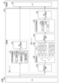
- FIG. 1 is a diagram showing an example of the configuration of an imaging device including an imaging element according to a first embodiment.
- FIG. 2 is a diagram illustrating an example of a pixel configuration of an imaging element according to the first embodiment.
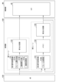
- 2 is a diagram illustrating an example of the configuration of a processing unit of an image sensor according to the first embodiment.
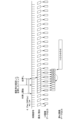
- FIG. 5A to 5C are diagrams illustrating an example of the operation of the imaging element according to the first embodiment.
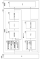
- FIG. 11 is a diagram illustrating an example of the configuration of a processing unit of an image sensor according to a second embodiment.
- 13A to 13C are diagrams illustrating an example of the operation of the imaging element according to the second embodiment.
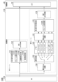
- FIG. 13 is a diagram illustrating an example of the configuration of a processing unit of an image sensor according to a third embodiment.
- FIGS. 13A to 13C are diagrams illustrating an example of the operation of the imaging element according to the third embodiment.
- FIG. 13 is a diagram illustrating an example of the configuration of a processing unit of an image sensor according to a modified example of the third embodiment.
- FIG. 13 is a diagram illustrating an example of the configuration of a processing unit of an image sensor according to a fourth embodiment.
- 13A to 13C are diagrams illustrating an example of the operation of an imaging element according to a fourth embodiment.
- 13A to 13C are diagrams illustrating an example of the operation of an image sensor according to Modification 1 of the fourth embodiment.
- 13A to 13C are diagrams illustrating an example of the operation of an image sensor according to Modification 2 of the fourth embodiment.
- Fig. 1 is a diagram showing a schematic configuration of an image sensor 1 including an image sensor 100 according to the first embodiment.
- the image sensor 1 is, for example, a digital camera, and includes an image sensor optical system 10, an operation unit 20, a recording unit 30, a control unit 40, a display unit 50, and the image sensor 100.
- the imaging optical system 10 is composed of multiple lenses, including a focus adjustment lens (focus lens), and an aperture, and forms an image of a subject on the imaging surface of the imaging element 100.
- the operation unit 20 includes a release button, a record button, various setting switches, etc.
- An operation signal corresponding to an operation on the operation unit 20 is sent to a control unit 40 such as a CPU.
- the control unit 40 controls the operation of each unit of the imaging device 1 in response to the received operation signal.
- the control unit 40 controls the imaging optical system 10 and the imaging element 100.
- the control unit 40 also sets the exposure period and the number of exposures, etc.
- the control unit 40 has an image generation unit (LSI) 42.
- the image generation unit 42 generates live view (LV) image data, still image data, and moving image data based on the image data output from the image sensor 100.
- the control unit 40 outputs the generated LV image data, still image data, or moving image data to the display unit 50.
- the LV image data output to the display unit 50 is an example of "image data for display.”
- the control unit 40 also outputs the generated still image data or moving image data to the recording unit 30.
- the image data output to the recording unit 30 is an example of "image data for recording.”
- the display unit 50 is, for example, an electronic viewfinder (EVF) or a rear monitor.
- EMF electronic viewfinder
- the display unit 50 displays images based on the LV image data, still image data, and video image data output from the control unit 40.
- the recording unit 30 records the still image data and video image data generated by the control unit 40 on a recording medium such as a memory card attached to the imaging device 1.
- the control unit 40 reads image data (still image data or moving image data) from the memory card in response to a user's operation of the operation unit 20.
- the control unit 40 outputs the read image data to the display unit 50.
- the display unit 50 displays (plays) an image based on the image data output from the control unit 40.
- the imaging element 100 is, for example, an image sensor such as a CCD or CMOS, and captures an image of a subject formed by the imaging optical system 10.
- the imaging element 100 performs exposure (imaging) during an exposure period set by the control unit 40.
- the imaging element 100 has a plurality of pixels 110, a plurality of AD converters (AD conversion units) 120, and a processing unit 130.
- the plurality of pixels 110 are arranged two-dimensionally (in the row and column directions) in the imaging element 100.
- Each of the plurality of pixels 110 has a color filter, a photoelectric conversion unit 112, and a readout circuit.
- the color filter is an optical member that transmits light of a specific wavelength, for example, R (red), G (green), or B (blue).
- the pixels 110 receive the light beam that has passed through the imaging optical system 10, and output an analog signal according to the amount of light received.
- the AD converter 120 converts the analog signal output from the pixels 110 into a digital signal.
- the processing unit 130 processes the digital signal converted by the AD converter 120. Note that while the AD converter 120 is shown as a single block in FIG. 1, the imaging element 100 includes multiple AD converters 120. An AD converter 120 is provided for each column of pixels 110.
- the pixel 110 has a photoelectric conversion unit 112 and a readout circuit 114.
- the photoelectric conversion unit 112 photoelectrically converts incident light to generate and accumulate electric charges.
- the photoelectric conversion unit 112 is composed of, for example, a photodiode.
- the readout circuit 114 reads out a pixel signal (analog signal) generated by the electric charges photoelectrically converted by the photoelectric conversion unit 112.
- the readout circuit 114 outputs the readout pixel signal to the AD converter 120.
- the above-mentioned image data is generated based on a plurality of pixel signals output from the plurality of pixels 110 and converted into digital signals.
- the exposure period is also a charge accumulation period during which the photoelectric conversion unit 112 photoelectrically converts light to accumulate electric charges.
- the readout circuit 114 has a transfer section 115, a discharge section 116, a floating diffusion 117, and an output section 118.
- the transfer section 115 transfers the charge photoelectrically converted by the photoelectric conversion section 112 to the floating diffusion 117.
- the floating diffusion 117 accumulates the charge photoelectrically converted by the photoelectric conversion section 112 through the transfer section 115.
- the floating diffusion 117 is a storage section that accumulates the charge.
- the output unit 118 has an amplifier unit 118A which is an amplifying transistor, and a selection unit 118B which is a selection transistor.
- the amplifier unit 118A generates a pixel signal from the charge of the floating diffusion 117.
- the selection unit 118B controls the connection between the pixel 110 and the signal line 119. When the selection unit 118B is set to on, the pixel signal generated by the amplifier unit 118A is output to the signal line 119.
- the discharge unit 116 discharges the charge in the floating diffusion 117 to the power supply VDD. By discharging the charge, the discharge unit 116 resets the potential of the floating diffusion 117 to the reference potential.
- the processing unit 130 has a first signal processing circuit 131, a first output circuit 132, a second signal processing circuit 133, a memory 134, and a second output circuit 135.
- first lane the combination of the first signal processing circuit 131 and the first output circuit 132
- second lane the combination of the second signal processing circuit 133, the memory 134, and the second output circuit 135
- the first lane is a circuit for outputting a signal for generating an LV image.
- the second lane is a circuit for outputting a signal for generating a still image.
- the first output circuit 132 is an example of a "first output unit”.
- the second output circuit 135 is an example of a "second output circuit”. Since the imaging element 100 has a first lane and a second lane, it can simultaneously (in parallel) process the signals used to generate the LV image and the signals used to generate the still image, and can simultaneously (in parallel) output them to the image generation unit 42.
- the first signal processing circuit 131 has a frame thinning section 131A, a pixel thinning section 131B, and a pixel summation section 131C.
- the first signal processing circuit 131 processes the digital signal output from the AD converter 120.
- the first signal processing circuit 131 receives digital signals corresponding to a plurality of pixels 110 included in the imaging area (effective pixel area) of the image sensor 100.
- the first signal processing circuit 131 performs a first signal processing on the input digital signal using the frame thinning section 131A, the pixel thinning section 131B, and the pixel summation section 131C.
- the frame thinning unit 131A performs a process of thinning frames on the input digital signal as the first signal processing.
- a frame refers to a frame (image data) used to generate LV image data, still image data, or moving image data.
- a frame is generated from a plurality of pixel signals output from a plurality of pixels 110 and converted into a digital signal by the AD converter 120.
- the digital signal input to the first signal processing circuit 131 is a frame used to generate image data, and the first signal processing circuit 131 performs the first signal processing on the input frame.
- “Thinning out frames” means using some of the multiple frames. Or, not using other frames.
- the frame thinning unit 131A selects frames generated during some of the multiple exposure periods (which are examples of the "first period,” “second period,” and “third period”). Or, the frame thinning unit 131A does not select frames generated during some of the multiple exposure periods.
- the frame thinning unit 131A performs frame thinning processing on the multiple signals output during the multiple exposure periods. By thinning the frames, the number of image data to be processed is reduced, and the amount of image data output from the image sensor 100 is reduced.
- the exposure period and the number of exposures are controlled by the control unit 40.
- the pixel thinning unit 131B performs a pixel thinning process on the digital signals corresponding to the multiple pixels 110 included in the imaging area output from the AD converter 120.
- "thinning out pixels” means using signals output from some of the pixels 110. Alternatively, it means not using signals output from other pixels 110.
- the pixel thinning unit 131B selects pixel signals output from some of the pixels 110 among the multiple pixel signals output from the multiple pixels 110 during a specified exposure period.
- the pixel thinning unit 131B does not select pixel signals output from some of the pixels 110 among the multiple pixel signals output from the multiple pixels 110 during a specified exposure period.
- the pixel thinning unit 131B performs a pixel thinning process on multiple signals (which are examples of the "first signal”, “second signal”, and “third signal”) output during multiple exposure periods. By thinning out pixels, the number of pixel signals to be processed is reduced, and the amount of image data output from the image sensor 100 is reduced.
- the pixel addition unit 131C performs pixel addition processing on the input digital signal as the first signal processing.
- pixel addition means adding signals output from any number of pixels (e.g., three pixels).
- the pixel addition unit 131C adds pixel signals output from some of the pixels 110 (e.g., three pixels) out of a plurality of pixel signals output from a plurality of pixels 110 during a specified exposure period.
- the pixel thinning processing reduces the number of pixel signals to be processed, and reduces the amount of image data output from the image sensor 100.
- the first signal processing circuit 131 performs frame thinning in the frame thinning section 131A, and then performs pixel thinning in the pixel thinning section 131B, or pixel addition in the pixel addition section 131C.
- the order of frame thinning, pixel thinning, and pixel addition is not limited to this.
- the first signal processing circuit 131 may perform frame thinning in the frame thinning section 131A, or pixel addition in the pixel addition section 131C, after thinning out pixels in the pixel thinning section 131B.
- the first signal processing circuit 131 does not have to perform all of frame thinning, pixel thinning, and pixel addition.
- the first signal processing circuit 131 it is sufficient for the first signal processing circuit 131 to perform at least one of frame thinning, pixel thinning, and pixel addition. Therefore, it is sufficient for the first signal processing circuit 131 to have at least one of the frame thinning section A, the pixel thinning section 131B, and the pixel addition section C.
- the frame thinning process, pixel thinning process, and pixel addition process are performed to reduce the amount of image data and the processing load.
- LV images are rarely required to be high quality images. Therefore, LV image data does not need to be generated using all of the pixel signals (digital signals) output from the multiple pixels 110 included in the imaging area.
- LV images are required to display new images on the display unit 50 at high speed. Therefore, the image sensor 100 is required to output image data at high speed.
- the control unit 40 is required to generate LV image data at high speed.
- the image sensor 100 performing the above process and reducing the amount of image data within the image sensor 100, communication between the image sensor 100 and the control unit 40 (image generation unit 42) is less likely to be limited by the upper limit of the interface bandwidth. This allows the image sensor 100 to output image data to the control unit 40 at high speed. In addition, since the amount of image data is small, the control unit 40 can reduce the processing load and generate LV image data at high speed.
- the first signal processing circuit 131 performs a first signal processing on the input digital signal, and then outputs the digital signal (frame) that has been subjected to the first signal processing to the first output circuit 132.
- the first output circuit 132 outputs the digital signal (frame) output from the first signal processing circuit 131 to the image generation unit 42.
- a digital signal (frame) for generating an LV image is output to the image generation unit 42.
- the second signal processing circuit 133 has a frame adder 133A.
- the second signal processing circuit 133 processes the digital signal output from the AD converter 120.
- the second signal processing circuit 133 receives digital signals corresponding to the pixels 110 included in the imaging area of the image sensor 100.
- the second signal processing circuit 133 performs second signal processing on the input digital signal using the frame adder 133A.
- the frame addition unit 133A performs addition processing on the digital signal output from the AD converter 120 as the second signal processing. In other words, the frame addition unit 133A performs addition processing on the input multiple frames as the second signal processing.
- the frame addition unit 133A adds multiple frames generated in each of the multiple exposures.
- the second signal processing circuit 133 acquires a first frame generated by exposure in the first exposure period from the AD converter 120 and outputs it to the memory 134.
- the memory 134 stores the first frame output from the second signal processing circuit 133.
- the second signal processing circuit 133 acquires a second frame generated by exposure in the second exposure period after the first exposure period from the AD converter 120. At that time, the second output circuit 135 reads out the first frame from the memory 134.
- the second output circuit 135 outputs the read out first frame to the second signal processing circuit 133.
- the frame addition unit 133A adds the first frame and the second frame.
- the second signal processing circuit 133 outputs the first added frame obtained by the addition to the memory 134.
- the memory 134 stores the first added frame output from the second signal processing circuit 133.
- the second signal processing circuit 133 acquires the third frame generated by exposure in the third exposure period after the second exposure period from the AD converter 120. At that time, the second output circuit 135 reads out the first added frame from the memory 134.
- the second output circuit 135 outputs the read out first added frame to the second signal processing circuit 133.
- the frame addition unit 133A adds the first added frame and the third frame.
- the second signal processing circuit outputs the second added frame obtained by the addition to the memory 134.
- the memory 134 stores the second added frame output from the second signal processing circuit 133.
- the second signal processing circuit 133, memory 134, and second output circuit 135 repeat the above process, so that the frame adder 133A can add multiple frames generated in each of the multiple exposure periods.
- the frame adder 133A performs second signal processing to add frames equal to the number of exposures set by the control unit 40. The exposure period and the number of exposures are controlled by the control unit 40.
- the second signal processing circuit 133 performs second signal processing on the input digital signal, and then outputs the digital signal (added frame) that has been subjected to the second signal processing to the second output circuit 135.
- the second output circuit 135 outputs the digital signal (added frame) output from the second signal processing circuit 133 to the image generation unit 42.
- a digital signal (frame) for generating a still image is output to the image generation unit 42.
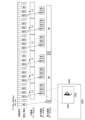
- FIG. 4 is a diagram showing an example of the operation of the image sensor 100 according to the first embodiment.
- FIG. 4 shows the output of still image data when the release button is pressed to capture a still image while LV image data is being output (while the display unit 50 is displaying an LV image).
- the LV image data is output continuously at regular time intervals, and the LV image is displayed continuously on the display unit 50 at regular time intervals.
- the image sensor 100 continuously outputs the LV image data at, for example, 8.34 ms intervals.
- the image sensor 100 continuously outputs frames for generating LV image data at a frame rate of 120 fps (frames per second). Therefore, the image sensor 100 repeatedly performs exposure/readout for a certain exposure period (for example, 4.17 ms) at regular time intervals (8.34 ms). In other words, the image sensor 100 repeatedly performs exposure/readout for a certain exposure period at a frame rate of 120 fps.
- the image sensor 100 reads out pixel signals only from some of the pixels 110 in the imaging area and outputs them to the AD converter 120 (pixel thinning readout).
- the image sensor 100 adds pixel signals output from the multiple pixels 110, reads them out, and outputs them to the AD converter 120 (pixel addition and readout).
- the pixel signals output to the AD converter 120 are output to the first signal processing circuit 131.
- the first output circuit 132 outputs the signal output from the first signal processing circuit 131 to the image generating unit 42.
- the first lane outputs image data for generating an LV image to the image generating unit 42.
- the first signal processing circuit 131 Before the release button is pressed, the first signal processing circuit 131 does not perform the first signal processing on the pixel signal. However, the image sensor 100 may output pixel signals from all pixels 110 included in the imaging area to the AD converter 120 without performing pixel thinning readout or pixel addition readout. In that case, even before the release button is pressed, the first signal processing circuit 131 (pixel thinning section 131B or pixel addition section 131C) performs the first signal processing (pixel thinning processing or pixel addition processing) on the pixel signal. The image sensor 100 may also output frames for generating LV image data at a frame rate of 240 fps.
- the image sensor 100 repeats exposure/readout for a fixed exposure period (e.g., 4.17 ms) at fixed time intervals (e.g., 4.17 ms).
- the first signal processing circuit 131 (frame thinning unit A) performs the first signal processing (frame thinning processing).
- the image sensor 100 When the release button is pressed to capture a still image, the image sensor 100 continuously outputs frames for generating LV image data and still image data. Therefore, the image sensor 100 repeats exposure/readout for a certain exposure period (e.g., 4.17 ms) at a certain time interval (e.g., 4.17 ms). In other words, the image sensor 100 repeats exposure/readout for a certain exposure period at a frame rate of 240 fps. Also, when the release button is pressed, the image sensor 100 outputs pixel signals from all pixels 110 included in the imaging area to the AD converter 120. The pixel signals output to the AD converter 120 are output to the first signal processing circuit 131. The first output circuit 132 outputs the signal output from the first signal processing circuit 131 to the image generation unit 42. The first lane outputs image data for generating an LV image to the image generation unit 42.
- a certain exposure period e.g., 4.17 ms
- a certain time interval e.g., 4.
- the first signal processing circuit 131 does not perform the first signal processing on the pixel signal.
- the image sensor 100 may output pixel signals from all pixels 110 included in the imaging area to the AD converter 120 without performing pixel thinning readout or pixel addition readout.
- the first signal processing circuit 131 (pixel thinning section 131B or pixel addition section 131C) performs the first signal processing (pixel thinning process or pixel addition process) on the pixel signal.
- FIG. 4 shows an example in which the image sensor 100 performs exposure/readout for a certain exposure period six times in succession.
- the image sensor 100 performs six exposures/readouts in succession and sequentially outputs six frames for generating an LV image and a still image. Also, when the release button is pressed, the image sensor 100 exposes all pixels included in the imaging area and outputs pixel signals. The six frames are output sequentially to the first and second lanes.
- the exposure period of the imaging element 100 may be longer than the exposure period for obtaining an LV image. If the exposure period for capturing a still image is, for example, 25 ms, the exposure period of the imaging element 100 will be longer than the exposure period for obtaining an LV image (4.17 ms). If the exposure period becomes longer than the exposure period for obtaining an LV image, the imaging element 100 will not be able to perform repeated exposure/readout to obtain an LV image, as it did before the release button was pressed.
- the imaging element 100 will not be able to output LV image data continuously at a fixed time interval (8.34 ms).
- the imaging device 1 will not be able to display LV images continuously on the display unit 50.
- the exposure period of the still image and the number of frames to be added are not limited to this.
- the exposure period of the still image and the number of frames to be added are appropriately set by the control unit 40 based on the shooting conditions (such as the brightness of the subject).
- the six frames sequentially output to the first lane are subjected to the first signal processing (frame thinning, pixel thinning, pixel addition) by the first signal processing circuit 131 (frame thinning section 131A, pixel thinning section 131B, pixel addition section 131C).
- the first signal processing circuit 131 performs the first signal processing on the input frames and outputs them to the first output circuit 132.
- the first output circuit 132 outputs the frames that have been subjected to the first signal processing to the image generation section 42.
- the first lane outputs image data for generating an LV image to the image generation section 42.
- the six frames sequentially output to the first lane are thinned out by the frame thinning section 131A. As a result, as shown in FIG. 4, the frames output to the first lane are continuously output at a frame rate of 120 fps, similar to before the release button was pressed.
- the six frames output to the second lane are subjected to second signal processing (frame addition processing) by the second signal processing circuit 133 (frame addition section 133A).
- the second signal processing circuit 133 performs second signal processing on the input multiple frames and outputs them to the second output circuit 135.
- the second output circuit 135 outputs the frames that have been subjected to the second signal processing to the image generation section 42.
- the second lane outputs image data for generating a still image to the image generation section 42.
- the image sensor 100 repeats exposure/readout for the same exposure period as before the release button was pressed. This allows the image sensor 100 to continuously output LV image data in the same manner as before the release button was pressed, and the image capture device 1 can display the LV image on the display unit 50.
- the image sensor 100 when the release button is pressed, the image sensor 100 performs frame thinning processing by the frame thinning unit 131A. Therefore, even if the exposure/readout of the image sensor 100 is performed at a frame rate of 240 fps, the image sensor 100 can continuously output the frames output to the first lane at a frame rate of 120 fps, similar to before the release button was pressed. Therefore, the processing load of the control unit 40 can be reduced. Also, when the release button is pressed, the image sensor 100 performs pixel thinning processing or pixel addition processing by the pixel thinning unit 131B or pixel addition unit 131C.
- the image sensor 100 can output the frames output to the first lane at high speed with the same amount of image data as before the release button was pressed. Therefore, the processing load of the control unit 40 can be reduced, and the control unit 40 can generate LV image data at high speed. This allows the display unit 50 to display the LV image at high speed without interrupting the display of the LV image, even if a still image is captured while the LV image is being displayed.
- the image sensor 100 adds multiple frames together using the frame adder 133A. This allows the image sensor 1 to obtain an image equivalent to a still image with a long exposure time even if the subject is dark. Even if the exposure period of the image sensor 100 is longer than the exposure period for obtaining an LV image in order to capture a still image of a dark subject, the image sensor 1 can capture the still image. In other words, the image sensor 1 can capture a still image while maintaining the display of the LV image.
- the image sensor 100 processes multiple frames in parallel in the first and second lanes, and outputs still image data and LV image data in parallel. This allows the image capture device 1 to display the LV images continuously in the same manner as before the release button was pressed, without interrupting the display of the LV images even when the release button is pressed.
- the image capture device 1 can also record the still image data in the recording unit 30.
- the processing unit 130 is implemented (on-chip) in the image sensor 100, not in the image generating unit 42.
- This allows the amount of LV image data or still image data to be reduced inside the image sensor 100 before the image sensor 100 outputs the LV image data or still image data to the image generating unit 42. Therefore, the time interval for outputting the LV image data or still image data is less likely to be limited by the upper limit of the bandwidth of the interface between the image sensor 100 and the image generating unit 42.
- This makes it possible to increase the number of exposures per unit time (the number of images taken per unit time) to obtain the LV image data and still image data. If the number of exposures per unit time increases, the number of frames output per unit time increases, and the addition process for generating still image data can be speeded up.
- the image sensor 100 according to the first embodiment achieves both display of an LV image and recording of still image data by adding a plurality of frames output to the second lane among the frames output to the first and second lanes.
- the image sensor 100A according to the second embodiment also adds frames output to the first lane.
- FIG. 5 is a diagram showing an example of the configuration of the processing unit 130 of the image sensor 100A according to the second embodiment.
- the configuration of the second lane of the processing unit 130 is similar to the configuration of the second lane of the processing unit 130 according to the first embodiment.
- the first lane of the processing unit 130 further includes an adder circuit 136 and a memory 137 in addition to the first signal processing circuit 131 and the first output circuit 132.
- the frame processed in the first lane is referred to as an LV image frame
- the frame processed in the second lane is referred to as a still image frame.
- the addition circuit 136 performs addition processing on the LV image frame output from the first signal processing circuit 131.
- the addition circuit 136 adds multiple LV image frames generated in each of the multiple exposures.
- the first signal processing circuit 131 acquires the first frame generated by exposure in the first exposure period from the AD converter 120 and performs the first signal processing.
- the first signal processing circuit 131 outputs the first LV image frame that has been subjected to the first signal processing to the memory 137 via the addition circuit 136.
- the memory 137 stores the first LV image frame output from the first signal processing circuit 131.
- the first signal processing circuit 131 acquires the second frame generated by exposure in the second exposure period after the first exposure period from the AD converter 120 and performs the first signal processing.
- the first signal processing circuit 131 outputs the second LV image frame that has been subjected to the first signal processing to the addition circuit 136.
- the first output circuit 132 reads out the first LV image frame from the memory 137.
- the first output circuit 132 outputs the read out first LV image frame to the adder circuit 136.
- the adder circuit 136 adds the first LV image frame and the second LV image frame.
- the adder circuit 136 outputs the first added LV image frame obtained by the addition to the memory 137.
- the memory 137 stores the first added LV image frame output from the adder circuit 136.
- the first signal processing circuit 131 acquires the third frame generated by exposure in the third exposure period after the second exposure period from the AD converter 120 and performs the first signal processing.
- the first signal processing circuit 131 outputs the third LV image frame that has been subjected to the first signal processing to the adder circuit 136.
- the first output circuit 132 reads out the first added LV image frame from the memory 137.
- the first output circuit 132 outputs the read first summed LV image frame to the adder circuit 136.
- the adder circuit 136 adds the first summed LV image frame and the third LV image frame.
- the adder circuit 136 outputs the second summed LV image frame obtained by the addition to the memory 137.
- the memory 137 stores the second summed LV image frame output from the adder circuit 136.
- the first signal processing circuit 131, the adder circuit 136, the memory 137, and the first output circuit 132 repeat the above processing, so that the adder circuit 136 can add a plurality of LV image frames generated in each of a plurality of exposure periods.
- the adder circuit 136A performs processing to add frames for the number of exposures set by the control unit 40. The exposure period and the number of exposures are controlled by the control unit 40.
- image data for generating an LV image is output to the image generating unit 42.
- the second signal processing circuit and memory 134 and the second output circuit 135 perform the same processing on the still image frames as in the first embodiment.
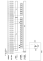
- FIG. 6 is a diagram showing an example of the operation of the image sensor 100A according to the second embodiment.
- FIG. 6 shows the output of still image data when the release button is pressed while LV image data is being output (while the display unit 50 is displaying an LV image).
- the LV image data is output continuously at regular time intervals, and the LV image is displayed continuously on the display unit 50 at regular time intervals.
- the imaging element 100 continuously outputs the LV image data, for example, at intervals of 16.68 ms. In other words, the imaging element 100 continuously outputs frames for generating LV image data at a frame rate of 60 fps. Therefore, the imaging element 100 repeatedly performs exposure/readout for a regular exposure period (for example, 4.17 ms). In other words, the imaging element 100 repeatedly performs exposure/readout for a regular exposure period at a frame rate of 240 fps.
- the addition circuit 136 sequentially adds the frames output from the first signal processing circuit 131.
- the first output circuit 132 outputs the frame obtained by adding the four frames to the image generation unit 42 as LV image data. This is because, when capturing a still image of a dark subject, for example, an exposure period of 4.17 ms may result in insufficient charge accumulation by the photoelectric conversion unit 112, and an LV image of sufficient image quality may not be output. Unlike the first embodiment, the addition circuit 136 adds four frames and outputs the result as an LV image, so that a high-quality LV image can be displayed even if the subject is dark, for example.
- the image sensor 100 When the release button is pressed to capture a still image, the image sensor 100 continuously outputs frames for generating still image data. That is, the image sensor 100 sequentially outputs six frames from among the frames exposed/read out at each fixed exposure period (e.g., 4.17 ms).
- the six frames output to the second lane are subjected to second signal processing (frame addition processing) by the second signal processing circuit 133 (frame addition section 133A).
- the second signal processing circuit 133 applies second signal processing to the input multiple frames and outputs them to the second output circuit 135.
- the second output circuit 135 outputs the frames that have been subjected to the second signal processing to the image generation section 42.
- the second lane outputs image data for generating a still image to the image generation section 42.
- the image sensor 100A performs an addition process on the frames for generating an LV image. This averages out the noise in the LV image data, and the image capture device 1 can obtain LV image data with reduced noise compared to when the addition process is not performed. As a result, the display unit 50 can display a high-quality LV image.
- the display unit 50 can display an LV image in which the signal value of the LV image data has been increased. Therefore, even if the subject is dark, the user can confirm the subject in the LV image.
- the imaging device 100 according to the first embodiment and the imaging device 100A according to the second embodiment output a frame for generating a still image to the second lane after the release button of the operation unit 20 is pressed (fully pressed) and perform an addition process.
- a time lag may occur between the timing when the user feels that he wants to shoot a still image and the timing when the user fully presses the release button.
- the timing when the user feels that he wants to shoot a still image may be earlier than the timing when the user fully presses the release button.
- the imaging device 100B according to the third embodiment detects that the release button is half-pressed and performs an addition process on a frame for generating a still image that was output a predetermined period before the timing when the release button was fully pressed.
- FIG. 7 is a diagram showing an example of the configuration of the processing unit 130 of the image sensor 100B according to the third embodiment.
- the configuration of the first lane of the processing unit 130 is similar to the configuration of the first lane of the processing unit 130 according to the first embodiment.
- the second lane of the processing unit 130 further includes a write circuit 138, a selection circuit 139, a memory 140, and a read circuit 141 in addition to a second signal processing circuit 133 and a second output circuit 135.
- the control unit 40 detects whether the release button of the operation unit 20 is pressed halfway or fully pressed based on the user's operation of the release button.
- the write circuit 138 When the write circuit 138 detects that the release button has been half-pressed, it sequentially stores the frames output in sequence to the second lane in the memory 140 selected by the selection circuit 139.
- the memory 140 can store the multiple frames output to the second lane.
- the memory 140 stores the frames output to the second lane in the order in which they were output while the release button is half-pressed.
- the read circuit 141 detects that the release button is fully pressed, it reads from the memory 140 the multiple frames that were output to the second lane a predetermined period of time before the timing when the full press was detected.
- the read circuit 141 reads from the memory 140 the multiple frames that were output to the second lane and stored in the memory 140 between the timing when the full press was detected and the timing when the full press was detected.
- the read circuit 141 outputs the multiple frames that it has read to the second signal processing circuit 133.
- the second signal processing circuit 133 uses the frame adder 133A to perform second signal processing on the multiple frames output from the readout circuit 141. As the second signal processing, the second signal processing circuit 133 performs addition processing on the multiple frames output from the readout circuit 141.
- the frame adder 133A performs second signal processing to add the number of frames set by the control unit 40.
- the second signal processing circuit 133 outputs the added frames to the second output circuit 135.
- the second output circuit 135 outputs the frames output from the second signal processing circuit 133 to the image generation unit 42. Through the above processing in the second lane, frames for generating a still image are output to the image generation unit 42.
- FIG. 8 is a diagram showing an example of the operation of the image sensor 100B according to the third embodiment.
- FIG. 8 shows the output of still image data when the release button is half-pressed while the display unit 50 is displaying an LV image, the half-pressed state continues for a predetermined period, and then the release button is fully pressed to capture a still image.
- the operation of the image sensor 100B in FIG. 8 is the same as that of the image sensor 100 according to the first embodiment, except for the operation related to half-pressing and full-pressing the release button. Below, we will explain the differences from the operation of the image sensor 100 according to the first embodiment.
- the image sensor 100 continuously outputs frames for generating LV image data and still image data.
- the continuously output frames are output in sequence to the first frame and the second lane.
- the multiple frames output to the second lane are stored in chronological order in the memory 140. Note that the multiple frames output to the first lane are the same as in the first embodiment, so a description thereof will be omitted.
- the readout circuit 141 When the release button is detected as being fully pressed after being half-pressed, the readout circuit 141 reads six frames from the memory 140, starting from the frame three frames before the timing when the full press was detected. The readout circuit 141 outputs the read frames to the second signal processing circuit 133. When the six frames are input from the readout circuit 141, the second signal processing circuit 133 adds the six frames using the frame addition unit 133A. The second signal processing circuit 133 outputs the frame obtained by the addition to the second output circuit 135. The second output circuit 135 outputs the frame input from the second signal processing circuit 133 to the image generation unit 42.
- the image sensor 100B when the image sensor 100B detects that the release button has been pressed halfway, it stores in the memory 140 a number of frames from the time when the halfway press was detected. After that, when the image sensor 100B detects that the release button has been pressed all the way, it adds up the number of frames stored in the memory 140, starting from a frame output a predetermined period before the time when the full press was detected. This allows the imaging device 1 to obtain still image data that eliminates the time lag between the actual release timing and the release timing intended by the user.
- the second signal processing circuit 133 of the image sensor 100B includes a memory 133B.
- the second signal processing circuit 133 adds the frames by storing the multiple frames sequentially input from the readout circuit 141 in the memory 133B.
- FIG. 9 is a diagram showing an example of the configuration of the processing unit 130 of the image sensor 100 according to the modified example of the third embodiment.
- the readout circuit 141 of the image sensor 100B according to the modified example of the third embodiment detects a full press of the release button
- the readout circuit 141 reads out a plurality of frames one by one from the memory 140 in order, starting from a frame outputted a predetermined period before the timing at which the full press was detected.
- the readout circuit 141 inputs the readout frames in order to the second signal processing circuit 133.
- the second signal processing circuit 133 stores the input frames in order in the memory 133B and adds them.
- the second signal processing circuit 133 outputs the frames added in the memory 133B to the second output circuit 135.
- a sequential addition process is performed on the frames output to the second lane for each time-division exposure time, thereby generating a still image for recording without interrupting the LV display by the display unit 50.
- the fourth embodiment utilizes surplus frames for other processes while maintaining both the LV display and recording still images.
- FIG. 10 is a diagram showing an example of the configuration of the processing unit 130 of the image sensor 100C according to the fourth embodiment.
- the configuration of the first lane of the processing unit 130 is similar to the configuration of the first lane of the processing unit 130 according to the first embodiment.
- the second signal processing circuit 133 has a readout unit 133C and a motion vector determination unit 133D instead of the frame addition unit 133A.
- the readout unit 133C reads out frames stored in the memory 140 at a predetermined frame rate and outputs the read out frames to the second output circuit 135.
- the second output circuit 135 outputs the frames received from the readout unit 133C to the image generation unit 42 as still images for recording.
- the motion vector determination unit 133D determines a motion vector based on the frames stored in the memory 140 and outputs a signal representing the pixel area corresponding to the motion vector to the second output circuit 135.
- the second output circuit 135 outputs the received signal to the image generation unit 42 as a frame corresponding to a partially enlarged image.
- FIG. 11 is a diagram showing an example of the operation of the image sensor 100C according to the fourth embodiment.
- each pixel 110 of the image sensor 100 is exposed by dividing it into a certain time-division exposure time (for example, at 4.17 ms intervals).
- a frame corresponding to a still image for recording is output to the memory 134 of the second lane, read by the readout unit 133C at a frame rate of 20 fps, and then output to the image generation unit 42.
- the other frames are output to the memory 134 of the second lane as frames corresponding to partial enlarged images, and after the motion vector is determined by the motion vector determination unit 133D, a frame representing a pixel area corresponding to the motion vector (a pixel area corresponding to 3000px ⁇ 2000px in the figure) is output to the image generation unit 42.
- the fourth embodiment it is possible to maintain the LV display and record still images while utilizing surplus frames for other processing.
- the surplus frames are used to generate a partial enlarged image of one moving part while maintaining the LV display and recording still images.
- the generation of the partial enlarged image is not limited to one moving part.
- a first modified example of the fourth embodiment generates two partial enlarged images of two moving parts while maintaining the LV display and recording still images.
- the configuration of the image sensor 100 is the same as that of the fourth embodiment, and is therefore not shown.
- FIG. 12 is a diagram showing an example of the operation of an image sensor 100C according to a modified example of the fourth embodiment.
- each pixel 110 of the image sensor 100 is exposed by dividing it into a fixed time-division exposure time (e.g., 2.08 ms intervals).
- a frame corresponding to a still image for recording is output to the memory 134 of the second lane, read by the readout unit 133C at a frame rate of 20 fps, and then output to the image generation unit 42.
- the other frames are output to the second lane memory 134 as frames corresponding to the partially enlarged image, and after the two motion vectors are determined by the motion vector determination unit 133D, frames representing the two pixel regions corresponding to the two motion vectors (in the figure, two pixel regions corresponding to 1500px x 1000px) are output to the image generation unit 42.
- multiple partial enlarged images can be generated while maintaining the LV display and recording still images.
- this modified example has been described as generating two partial enlarged images relating to two moving parts, the present invention is not limited to such a configuration. Even when generating multiple partial enlarged images relating to three or more moving parts, frames corresponding to the partial enlarged images are output to the second lane memory 134 at a predetermined frame rate, and frames representing multiple pixel regions corresponding to multiple motion vectors are output to the image generation unit 42.
- the surplus frames are used to generate a partial enlarged image while maintaining the LV display and recording a still image.
- the use of the surplus frames is not limited to generating a partial enlarged image.
- the second modified example of the fourth embodiment enables detection of flicker while maintaining the LV display and recording a still image.
- the image sensor 100C according to the second modified example of the fourth embodiment has a flicker detection unit instead of the motion vector determination unit 133D in the configuration shown in FIG. 10.
- FIG. 13 is a diagram showing an example of the operation of an image sensor 100C according to a modified example of the fourth embodiment.
- each pixel 110 of the image sensor 100 is exposed by dividing it into a certain time-division exposure time (for example, at 1.04 ms intervals).
- a frame corresponding to a still image for recording is output to the memory 134 of the second lane, read by the readout unit 133C at a frame rate of 20 fps, and then output to the image generation unit 42.
- the other frames are output to the memory 134 of the second lane as frames corresponding to images for flicker detection.
- the flicker detection unit detects the period of the luminance change of the light source, i.e., flicker, based on the frame.
- the flicker detection unit outputs a frame representing a pixel area corresponding to the detected flicker (two pixel areas corresponding to 1500px x 1000px in the figure) to the second output circuit 135.
- the second output circuit 135 outputs the frame representing the flicker to the image generation unit 42.
- the frame representing the flicker output at this time is also output to a control unit arranged outside the image sensor 100, and the control unit may control the image sensor 100 to adjust the shutter speed, for example, to eliminate the flicker, based on the received frame.
- the frame representing the flicker may also be output to a control unit, such as a vertical scanning circuit, installed inside the image sensor 100, and the control unit may control the image sensor 100 to eliminate the flicker.
- flicker can be detected while maintaining the LV display and recording still images.
- the second signal processing circuit 133 for recording a still image reads out the surplus frames from the AD converter 120 and uses them to generate a partial enlarged image and detect flicker. That is, the second signal processing circuit 133 reads out both the frames for recording a still image and the surplus frames for generating a partial enlarged image and detecting flicker.
- the processing unit 130 may independently include the second signal processing circuit 133 for recording a still image and a third signal processing circuit for generating a partial enlarged image and detecting flicker. In that case, the processing unit 130 may further include a third output unit that outputs a signal output by the third signal processing circuit to the image generating unit 42.
- the processing unit 130 has a first signal processing circuit 131, a first output circuit 132, a second signal processing circuit 133, a second output circuit 135, a third signal processing circuit, and a third output unit.
- the processing unit 130 may not have the second signal processing circuit 133 and the second output circuit 135 for recording still images, but may have only the first signal processing circuit 131, the first output circuit 132, the third signal processing circuit, and the third output unit.
- the first signal processing circuit 131 outputs some of the multiple signals output from the AD converter 120 to the image generation unit 42 as the first signal processing.
- the present invention is not limited to such a configuration, and the first signal processing circuit 131 may perform a predetermined process on some of the multiple signals output from the AD converter 120 as the first signal processing. In that case, the first signal processing circuit 131 may perform processes such as debayering, color interpolation, and tone correction on the some of the signals as the first signal processing.
- the second signal processing circuit 133 adds frames in multiple different exposure periods output from the AD converter 120 as the second signal processing.
- the present invention is not limited to such a configuration, and the second signal processing circuit 133 may perform, for example, a process of recording (outputting) the added frame to a recording circuit as the second signal processing.
- the second signal processing circuit 133 may perform, as the second signal processing, processes such as debayering, color interpolation, and tone correction on the added frame or on multiple frames before addition.
- the components of the pixel 110 and the processing unit 130 are provided on a single substrate.
- the present invention is not limited to such a configuration, and the components of the pixel 110 and the processing unit 130 may be provided on multiple substrates that are joined to each other.
- the image sensor 100 may have a layered structure in which multiple substrates are stacked.
- the imaging element 100 may have a first substrate on which a plurality of pixels 110 are provided, and a second substrate bonded to the first substrate and on which a plurality of AD converters 120 and a processing unit 130 are provided.
- the imaging element 100 may have a first substrate on which a plurality of pixels 110 and a plurality of AD converters 120 are provided, and a second substrate bonded to the first substrate and on which a processing unit 130 is provided.
- the imaging element 100 may have a first substrate on which a plurality of pixels 110, a plurality of AD converters 120, a first signal processing circuit 131, and a first output circuit 132 are provided, and a second substrate bonded to the first substrate and on which a second signal processing circuit 133 and a second output circuit 135 are provided.
- the stacked structure of the imaging element 100 is not limited to a two-layer structure, and the imaging element 100 may have a stacked structure of three layers, four layers, or more.
- the imaging element 100 may have a first substrate on which a plurality of pixels 110 are provided, a second substrate bonded to the first substrate and on which a plurality of AD converters 120 are provided, and a third substrate bonded to the second substrate and on which a processing unit 130 is provided.
- the imaging element 100 may have a first substrate on which a plurality of pixels 110 and a plurality of AD converters 120 are provided, a second substrate bonded to the first substrate and on which a first signal processing circuit 131 and a first output circuit 132 are provided, and a third substrate bonded to the second substrate and on which a second signal processing circuit 133 and a second output circuit 135 are provided.
- the image sensor 100 may have a first substrate on which a plurality of pixels 110 are provided, a second substrate bonded to the first substrate and on which a plurality of AD converters 120 are provided, a third substrate bonded to the second substrate and on which a first signal processing circuit 131 and a first output circuit 132 are provided, and a fourth substrate bonded to the third substrate and on which a second signal processing circuit 133 and a second output circuit 135 are provided.
- the pixels 110 and the components of the processing unit 130 may be provided in any combination on any number of substrates.
Landscapes
- Engineering & Computer Science (AREA)
- Multimedia (AREA)
- Signal Processing (AREA)
- Transforming Light Signals Into Electric Signals (AREA)
- Studio Devices (AREA)
Priority Applications (2)
| Application Number | Priority Date | Filing Date | Title |
|---|---|---|---|
| CN202480019639.6A CN120937385A (zh) | 2023-03-28 | 2024-03-28 | 摄像元件及摄像装置 |
| JP2025511194A JPWO2024204600A1 (cg-RX-API-DMAC7.html) | 2023-03-28 | 2024-03-28 |
Applications Claiming Priority (2)
| Application Number | Priority Date | Filing Date | Title |
|---|---|---|---|
| JP2023-051434 | 2023-03-28 | ||
| JP2023051434 | 2023-03-28 |
Publications (1)
| Publication Number | Publication Date |
|---|---|
| WO2024204600A1 true WO2024204600A1 (ja) | 2024-10-03 |
Family
ID=92906822
Family Applications (1)
| Application Number | Title | Priority Date | Filing Date |
|---|---|---|---|
| PCT/JP2024/012785 Ceased WO2024204600A1 (ja) | 2023-03-28 | 2024-03-28 | 撮像素子および撮像装置 |
Country Status (3)
| Country | Link |
|---|---|
| JP (1) | JPWO2024204600A1 (cg-RX-API-DMAC7.html) |
| CN (1) | CN120937385A (cg-RX-API-DMAC7.html) |
| WO (1) | WO2024204600A1 (cg-RX-API-DMAC7.html) |
Citations (7)
| Publication number | Priority date | Publication date | Assignee | Title |
|---|---|---|---|---|
| JP2008205620A (ja) * | 2007-02-16 | 2008-09-04 | Canon Inc | 撮像装置及び撮像装置の制御方法 |
| JP2009212909A (ja) * | 2008-03-05 | 2009-09-17 | Sharp Corp | 固体撮像装置、固体撮像装置のフリッカ検出方法、制御プログラム、可読記録媒体および電子情報機器 |
| WO2015022900A1 (ja) * | 2013-08-12 | 2015-02-19 | 株式会社ニコン | 電子機器、電子機器の制御方法、及び制御プログラム |
| JP2017204784A (ja) * | 2016-05-12 | 2017-11-16 | キヤノン株式会社 | 撮像装置およびその制御方法、プログラム、並びに記憶媒体 |
| WO2018030137A1 (ja) * | 2016-08-08 | 2018-02-15 | ソニーセミコンダクタソリューションズ株式会社 | 撮像装置、電子機器 |
| WO2018066306A1 (ja) * | 2016-10-04 | 2018-04-12 | 富士フイルム株式会社 | 撮像装置、静止画撮像方法、及び、静止画撮像プログラム |
| JP2020098968A (ja) * | 2018-12-17 | 2020-06-25 | オリンパス株式会社 | 撮像素子、撮像装置、および撮像方法 |
Family Cites Families (4)
| Publication number | Priority date | Publication date | Assignee | Title |
|---|---|---|---|---|
| US20030169818A1 (en) * | 2002-03-06 | 2003-09-11 | Pere Obrador | Video transcoder based joint video and still image pipeline with still burst mode |
| JP2005184339A (ja) * | 2003-12-18 | 2005-07-07 | Canon Inc | 撮像装置 |
| JP2013187890A (ja) * | 2012-03-12 | 2013-09-19 | Sony Corp | 画像処理装置と画像処理方法 |
| JP2013211715A (ja) * | 2012-03-30 | 2013-10-10 | Nikon Corp | 撮像装置 |
-
2024
- 2024-03-28 CN CN202480019639.6A patent/CN120937385A/zh active Pending
- 2024-03-28 WO PCT/JP2024/012785 patent/WO2024204600A1/ja not_active Ceased
- 2024-03-28 JP JP2025511194A patent/JPWO2024204600A1/ja active Pending
Patent Citations (7)
| Publication number | Priority date | Publication date | Assignee | Title |
|---|---|---|---|---|
| JP2008205620A (ja) * | 2007-02-16 | 2008-09-04 | Canon Inc | 撮像装置及び撮像装置の制御方法 |
| JP2009212909A (ja) * | 2008-03-05 | 2009-09-17 | Sharp Corp | 固体撮像装置、固体撮像装置のフリッカ検出方法、制御プログラム、可読記録媒体および電子情報機器 |
| WO2015022900A1 (ja) * | 2013-08-12 | 2015-02-19 | 株式会社ニコン | 電子機器、電子機器の制御方法、及び制御プログラム |
| JP2017204784A (ja) * | 2016-05-12 | 2017-11-16 | キヤノン株式会社 | 撮像装置およびその制御方法、プログラム、並びに記憶媒体 |
| WO2018030137A1 (ja) * | 2016-08-08 | 2018-02-15 | ソニーセミコンダクタソリューションズ株式会社 | 撮像装置、電子機器 |
| WO2018066306A1 (ja) * | 2016-10-04 | 2018-04-12 | 富士フイルム株式会社 | 撮像装置、静止画撮像方法、及び、静止画撮像プログラム |
| JP2020098968A (ja) * | 2018-12-17 | 2020-06-25 | オリンパス株式会社 | 撮像素子、撮像装置、および撮像方法 |
Also Published As
| Publication number | Publication date |
|---|---|
| CN120937385A (zh) | 2025-11-11 |
| JPWO2024204600A1 (cg-RX-API-DMAC7.html) | 2024-10-03 |
Similar Documents
| Publication | Publication Date | Title |
|---|---|---|
| CN103168463B (zh) | 图像传感器和摄像设备 | |
| JP5319347B2 (ja) | 撮像装置及びその制御方法 | |
| CN105049685B (zh) | 摄像设备和摄像设备的控制方法 | |
| CN101795354B (zh) | 摄像装置和摄像方法 | |
| US8111298B2 (en) | Imaging circuit and image pickup device | |
| US11290648B2 (en) | Image capture apparatus and control method thereof | |
| US12542977B2 (en) | Imaging device for performing focus adjustment of optical system | |
| JP4622790B2 (ja) | 撮像素子および撮像装置 | |
| US7609306B2 (en) | Solid-state image pickup apparatus with high- and low-sensitivity photosensitive cells, and an image shooting method using the same | |
| JP2009021985A (ja) | 撮像装置及び撮像装置の駆動方法 | |
| US12382200B2 (en) | Image capturing circuit that can be applied to image capturing apparatus | |
| JP4199381B2 (ja) | 固体撮像装置および固体撮像素子駆動方法 | |
| CN120937385A (zh) | 摄像元件及摄像装置 | |
| JP2004120391A (ja) | 固体撮像装置 | |
| JP5072466B2 (ja) | 撮像装置 | |
| JP2010166159A (ja) | カメラ、カメラのぶれ補正方法 | |
| JP2007088842A (ja) | 撮像装置、および撮像素子の駆動方法 | |
| JP2018110433A (ja) | 撮像装置 | |
| JP2005117276A (ja) | 撮像装置 | |
| JP6354867B2 (ja) | 撮像装置 | |
| JP4618280B2 (ja) | 電子カメラ | |
| JP2004297449A (ja) | 固体撮像装置およびシェーディング補正方法 | |
| JP2020061759A (ja) | 撮像装置 | |
| JP2007166319A (ja) | 撮像ユニット及び撮像装置 | |
| JP2007174474A (ja) | 撮像装置 |
Legal Events
| Date | Code | Title | Description |
|---|---|---|---|
| 121 | Ep: the epo has been informed by wipo that ep was designated in this application |
Ref document number: 24780699 Country of ref document: EP Kind code of ref document: A1 |
|
| ENP | Entry into the national phase |
Ref document number: 2025511194 Country of ref document: JP Kind code of ref document: A |
|
| WWE | Wipo information: entry into national phase |
Ref document number: 2025511194 Country of ref document: JP |
|
| NENP | Non-entry into the national phase |
Ref country code: DE |
|
| 122 | Ep: pct application non-entry in european phase |
Ref document number: 24780699 Country of ref document: EP Kind code of ref document: A1 |