WO2024204590A1 - 半導体装置 - Google Patents
半導体装置 Download PDFInfo
- Publication number
- WO2024204590A1 WO2024204590A1 PCT/JP2024/012749 JP2024012749W WO2024204590A1 WO 2024204590 A1 WO2024204590 A1 WO 2024204590A1 JP 2024012749 W JP2024012749 W JP 2024012749W WO 2024204590 A1 WO2024204590 A1 WO 2024204590A1
- Authority
- WO
- WIPO (PCT)
- Prior art keywords
- wiring
- wirings
- pad
- region
- less
- Prior art date
- Legal status (The legal status is an assumption and is not a legal conclusion. Google has not performed a legal analysis and makes no representation as to the accuracy of the status listed.)
- Ceased
Links
Images


Classifications
-
- H—ELECTRICITY
- H10—SEMICONDUCTOR DEVICES; ELECTRIC SOLID-STATE DEVICES NOT OTHERWISE PROVIDED FOR
- H10W—GENERIC PACKAGES, INTERCONNECTIONS, CONNECTORS OR OTHER CONSTRUCTIONAL DETAILS OF DEVICES COVERED BY CLASS H10
- H10W20/00—Interconnections in chips, wafers or substrates
- H10W20/20—Interconnections within wafers or substrates, e.g. through-silicon vias [TSV]
-
- H—ELECTRICITY
- H10—SEMICONDUCTOR DEVICES; ELECTRIC SOLID-STATE DEVICES NOT OTHERWISE PROVIDED FOR
- H10D—INORGANIC ELECTRIC SEMICONDUCTOR DEVICES
- H10D12/00—Bipolar devices controlled by the field effect, e.g. insulated-gate bipolar transistors [IGBT]
-
- H—ELECTRICITY
- H10—SEMICONDUCTOR DEVICES; ELECTRIC SOLID-STATE DEVICES NOT OTHERWISE PROVIDED FOR
- H10D—INORGANIC ELECTRIC SEMICONDUCTOR DEVICES
- H10D30/00—Field-effect transistors [FET]
- H10D30/01—Manufacture or treatment
- H10D30/021—Manufacture or treatment of FETs having insulated gates [IGFET]
-
- H—ELECTRICITY
- H10—SEMICONDUCTOR DEVICES; ELECTRIC SOLID-STATE DEVICES NOT OTHERWISE PROVIDED FOR
- H10D—INORGANIC ELECTRIC SEMICONDUCTOR DEVICES
- H10D30/00—Field-effect transistors [FET]
- H10D30/60—Insulated-gate field-effect transistors [IGFET]
-
- H—ELECTRICITY
- H10—SEMICONDUCTOR DEVICES; ELECTRIC SOLID-STATE DEVICES NOT OTHERWISE PROVIDED FOR
- H10D—INORGANIC ELECTRIC SEMICONDUCTOR DEVICES
- H10D62/00—Semiconductor bodies, or regions thereof, of devices having potential barriers
- H10D62/10—Shapes, relative sizes or dispositions of the regions of the semiconductor bodies; Shapes of the semiconductor bodies
-
- H—ELECTRICITY
- H10—SEMICONDUCTOR DEVICES; ELECTRIC SOLID-STATE DEVICES NOT OTHERWISE PROVIDED FOR
- H10D—INORGANIC ELECTRIC SEMICONDUCTOR DEVICES
- H10D62/00—Semiconductor bodies, or regions thereof, of devices having potential barriers
- H10D62/80—Semiconductor bodies, or regions thereof, of devices having potential barriers characterised by the materials
- H10D62/81—Semiconductor bodies, or regions thereof, of devices having potential barriers characterised by the materials of structures exhibiting quantum-confinement effects, e.g. single quantum wells; of structures having periodic or quasi-periodic potential variation
-
- H—ELECTRICITY
- H10—SEMICONDUCTOR DEVICES; ELECTRIC SOLID-STATE DEVICES NOT OTHERWISE PROVIDED FOR
- H10D—INORGANIC ELECTRIC SEMICONDUCTOR DEVICES
- H10D64/00—Electrodes of devices having potential barriers
- H10D64/20—Electrodes characterised by their shapes, relative sizes or dispositions
-
- H—ELECTRICITY
- H10—SEMICONDUCTOR DEVICES; ELECTRIC SOLID-STATE DEVICES NOT OTHERWISE PROVIDED FOR
- H10D—INORGANIC ELECTRIC SEMICONDUCTOR DEVICES
- H10D64/00—Electrodes of devices having potential barriers
- H10D64/20—Electrodes characterised by their shapes, relative sizes or dispositions
- H10D64/27—Electrodes not carrying the current to be rectified, amplified, oscillated or switched, e.g. gates
-
- H—ELECTRICITY
- H10—SEMICONDUCTOR DEVICES; ELECTRIC SOLID-STATE DEVICES NOT OTHERWISE PROVIDED FOR
- H10D—INORGANIC ELECTRIC SEMICONDUCTOR DEVICES
- H10D64/00—Electrodes of devices having potential barriers
- H10D64/60—Electrodes characterised by their materials
- H10D64/66—Electrodes having a conductor capacitively coupled to a semiconductor by an insulator, e.g. MIS electrodes
-
- H—ELECTRICITY
- H10—SEMICONDUCTOR DEVICES; ELECTRIC SOLID-STATE DEVICES NOT OTHERWISE PROVIDED FOR
- H10D—INORGANIC ELECTRIC SEMICONDUCTOR DEVICES
- H10D84/00—Integrated devices formed in or on semiconductor substrates that comprise only semiconducting layers, e.g. on Si wafers or on GaAs-on-Si wafers
- H10D84/01—Manufacture or treatment
- H10D84/02—Manufacture or treatment characterised by using material-based technologies
- H10D84/03—Manufacture or treatment characterised by using material-based technologies using Group IV technology, e.g. silicon technology or silicon-carbide [SiC] technology
- H10D84/038—Manufacture or treatment characterised by using material-based technologies using Group IV technology, e.g. silicon technology or silicon-carbide [SiC] technology using silicon technology, e.g. SiGe
-
- H—ELECTRICITY
- H10—SEMICONDUCTOR DEVICES; ELECTRIC SOLID-STATE DEVICES NOT OTHERWISE PROVIDED FOR
- H10P—GENERIC PROCESSES OR APPARATUS FOR THE MANUFACTURE OR TREATMENT OF DEVICES COVERED BY CLASS H10
- H10P14/00—Formation of materials, e.g. in the shape of layers or pillars
- H10P14/40—Formation of materials, e.g. in the shape of layers or pillars of conductive or resistive materials
-
- H—ELECTRICITY
- H10—SEMICONDUCTOR DEVICES; ELECTRIC SOLID-STATE DEVICES NOT OTHERWISE PROVIDED FOR
- H10W—GENERIC PACKAGES, INTERCONNECTIONS, CONNECTORS OR OTHER CONSTRUCTIONAL DETAILS OF DEVICES COVERED BY CLASS H10
- H10W20/00—Interconnections in chips, wafers or substrates
- H10W20/01—Manufacture or treatment
-
- H—ELECTRICITY
- H10—SEMICONDUCTOR DEVICES; ELECTRIC SOLID-STATE DEVICES NOT OTHERWISE PROVIDED FOR
- H10W—GENERIC PACKAGES, INTERCONNECTIONS, CONNECTORS OR OTHER CONSTRUCTIONAL DETAILS OF DEVICES COVERED BY CLASS H10
- H10W20/00—Interconnections in chips, wafers or substrates
- H10W20/40—Interconnections external to wafers or substrates, e.g. back-end-of-line [BEOL] metallisations or vias connecting to gate electrodes
-
- H—ELECTRICITY
- H10—SEMICONDUCTOR DEVICES; ELECTRIC SOLID-STATE DEVICES NOT OTHERWISE PROVIDED FOR
- H10W—GENERIC PACKAGES, INTERCONNECTIONS, CONNECTORS OR OTHER CONSTRUCTIONAL DETAILS OF DEVICES COVERED BY CLASS H10
- H10W72/00—Interconnections or connectors in packages
- H10W72/20—Bump connectors, e.g. solder bumps or copper pillars; Dummy bumps; Thermal bumps
- H10W72/241—Dispositions, e.g. layouts
- H10W72/244—Dispositions, e.g. layouts relative to underlying supporting features, e.g. bond pads, RDLs or vias
-
- H—ELECTRICITY
- H10—SEMICONDUCTOR DEVICES; ELECTRIC SOLID-STATE DEVICES NOT OTHERWISE PROVIDED FOR
- H10W—GENERIC PACKAGES, INTERCONNECTIONS, CONNECTORS OR OTHER CONSTRUCTIONAL DETAILS OF DEVICES COVERED BY CLASS H10
- H10W72/00—Interconnections or connectors in packages
- H10W72/20—Bump connectors, e.g. solder bumps or copper pillars; Dummy bumps; Thermal bumps
- H10W72/241—Dispositions, e.g. layouts
- H10W72/247—Dispositions of multiple bumps
- H10W72/248—Top-view layouts, e.g. mirror arrays
-
- H—ELECTRICITY
- H10—SEMICONDUCTOR DEVICES; ELECTRIC SOLID-STATE DEVICES NOT OTHERWISE PROVIDED FOR
- H10W—GENERIC PACKAGES, INTERCONNECTIONS, CONNECTORS OR OTHER CONSTRUCTIONAL DETAILS OF DEVICES COVERED BY CLASS H10
- H10W72/00—Interconnections or connectors in packages
- H10W72/90—Bond pads, in general
- H10W72/941—Dispositions of bond pads
- H10W72/944—Dispositions of multiple bond pads
- H10W72/9445—Top-view layouts, e.g. mirror arrays
Definitions
- Patent Document 1 discloses a semiconductor device including a source pad electrode, a drain pad electrode, multiple source electrodes, and multiple drain electrodes arranged two-dimensionally on the same insulating film.
- the multiple source electrodes are extended from the source pad electrode onto the insulating film in a comb-tooth shape and are electrically connected to the source region through the insulating film.
- the multiple drain electrodes are extended from the drain pad electrode onto the insulating film in a comb-like shape that meshes with the multiple source electrodes, and are electrically connected to the drain region through the insulating film.
- This semiconductor device has a relatively long wiring distance and a relatively high wiring resistance between the source pad electrode and the drain pad electrode.
- This disclosure provides a semiconductor device with a novel wiring layout.
- the present disclosure provides a semiconductor device including: a wiring group including a plurality of first lower wirings and a plurality of second lower wirings arranged in a striped pattern extending in a first direction X; a first pad wiring arranged on at least one of the first lower wirings; a second pad wiring arranged on at least one of the second lower wirings at a distance from the first pad wiring in a second direction Y intersecting the first direction X; at least one first outgoing wiring drawn from the first pad wiring in the second direction Y and electrically connected to at least one of the first under wirings in a region between the first pad wiring and the second pad wiring; and at least one second outgoing wiring drawn from the second pad wiring in the second direction Y and electrically connected to at least one of the second under wirings in a region between the first pad wiring and the second pad wiring.
- the present disclosure provides a semiconductor device including one and the other wiring groups arranged at intervals in a first direction X, the one and the other wiring groups each including a plurality of first lower wirings and a plurality of second lower wirings arranged in stripes extending in the first direction X, a first pad wiring arranged on the one and the other wiring groups and electrically connected to at least one of the first lower wirings of each of the wiring groups, and a second pad wiring arranged on the one and the other wiring groups at an interval from the first pad wiring in a second direction Y intersecting the first direction X, and electrically connected to at least one of the second lower wirings of each of the wiring groups.
- the present disclosure provides a semiconductor device including one and the other wiring groups arranged at a distance from each other, the one and the other wiring groups each including a plurality of first lower wirings and a plurality of second lower wirings, an inter-wiring area partitioned between the one and the other wiring groups, a first pad wiring arranged on the inter-wiring area, a second pad wiring spaced from the first pad wiring and arranged on the inter-wiring area, a first pull-out wiring drawn from the first pad wiring to an area outside the inter-wiring area and electrically connected to the first lower wiring of one of the wiring groups, and a second pull-out wiring drawn from the second pad wiring to an area outside the inter-wiring area so as to face the first pull-out wiring across the inter-wiring area and electrically connected to the second lower wiring of the other wiring group.
- the present disclosure provides a semiconductor device including: a plurality of wiring groups arranged at intervals in a first direction X, each of the wiring groups including a plurality of first lower wirings and a plurality of second lower wirings; an inter-wiring area partitioned into a strip extending in a second direction Y intersecting the first direction X between the plurality of wiring groups; an intermediate wiring arranged in the inter-wiring area and electrically separated from the plurality of wiring groups; and an intermediate pad wiring arranged on the intermediate wiring, electrically separated from the plurality of wiring groups, and electrically connected to the intermediate wiring.
- the present disclosure provides a semiconductor device including a chip, a plurality of active regions formed on the chip at intervals in a first direction X, a boundary region formed in a strip shape extending in a second direction Y intersecting the first direction X between the plurality of active regions on the chip, intermediate wiring arranged on the boundary region, and intermediate pad wiring arranged on the intermediate wiring and electrically connected to the intermediate wiring.
- the present disclosure provides a semiconductor device including: a wiring group including a plurality of first lower wirings and a plurality of second lower wirings arranged in stripes extending in a first direction X; a first pad wiring arranged on at least one of the first lower wirings; a second pad wiring arranged on at least one of the second lower wirings at a distance from the first pad wiring in a second direction Y intersecting the first direction X; an inter-pad region partitioned between the first pad wiring and the second pad wiring; a first side wiring drawn from the first pad wiring to a region facing the inter-pad region on one side of the first direction X and electrically connected to at least one of the first lower wirings passing through the inter-pad region; and a second side wiring drawn from the second pad wiring to a region facing the inter-pad region on one side of the first direction X and electrically connected to at least one of the second lower wirings passing through the inter-pad region.
- the present disclosure provides a semiconductor device including a chip having a first main surface on one side and a second main surface on the other side, a base layer of a first conductivity type formed on the second main surface side within the chip, a drift layer of a second conductivity type formed on the first main surface side within the chip, a plurality of trench electrode type gate structures formed on the first main surface so as to be positioned within the drift layer, a plurality of drain source regions of a second conductivity type formed in regions between the plurality of gate structures in a surface layer portion of the drift layer, and a plurality of impurity regions of a first conductivity type formed in regions along the lower ends of the plurality of gate structures.
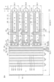
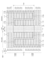
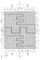
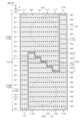
- FIG. 1 is a plan view showing a semiconductor device according to a first embodiment.
- FIG. 2 is a cross-sectional view taken along the line II-II shown in FIG.
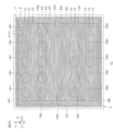
- FIG. 3 is a plan view showing an example of the layout of the first main surface.
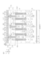
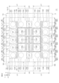
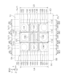
- FIG. 4 is an enlarged plan view showing a main portion of the first main surface.
- FIG. 5 is an enlarged plan view showing a main portion of the first main surface.
- FIG. 6 is an enlarged plan view showing a main portion of the first main surface.
- FIG. 7 is a cross-sectional view taken along line VII-VII shown in FIG.
- FIG. 8 is a cross-sectional view taken along line VIII-VIII shown in FIG.
- FIG. 9 is a cross-sectional view taken along line IX-IX shown in FIG.
- FIG. 1 is a plan view showing a semiconductor device according to a first embodiment.
- FIG. 2 is a cross-sectional view taken along the line II-II shown in FIG.
- FIG. 10 is a cross-sectional view taken along line X-X shown in FIG.
- FIG. 11 is a cross-sectional view taken along the line XI-XI shown in FIG.
- FIG. 12 is a cross-sectional view taken along the line XII-XII shown in FIG.
- FIG. 13 is a cross-sectional view taken along the line XIII-XIII shown in FIG.
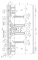
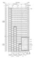
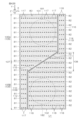
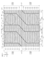
- FIG. 14 is a plan view showing an example of the layout of the first layer wiring.
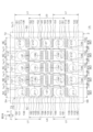
- FIG. 15 is a plan view showing an example of the layout of the second layer wiring.
- FIG. 16A is an enlarged plan view showing a first wiring unit according to the first example.
- FIG. 16B is an enlarged plan view showing the first wiring unit according to the second example.
- FIG. 16A is an enlarged plan view showing a first wiring unit according to the first example.
- FIG. 16B is an enlarged plan view showing the first wiring unit according to the second example.
- FIG. 16A is an enlarged plan
- FIG. 16C is an enlarged plan view showing a first wiring unit according to the third example.
- FIG. 16D is an enlarged plan view showing a first wiring unit according to the fourth example.
- FIG. 16E is an enlarged plan view showing a first wiring unit according to the fifth example.
- FIG. 16F is an enlarged plan view showing a first wiring unit according to the sixth example.
- FIG. 16G is an enlarged plan view showing a first wiring unit according to the seventh example.
- FIG. 16H is an enlarged plan view showing a first wiring unit according to the eighth example.
- FIG. 16I is an enlarged plan view showing a first wiring unit according to a ninth example.
- FIG. 16J is an enlarged plan view showing a first wiring unit according to a tenth example.
- FIG. 17A is an enlarged plan view showing a second wiring unit according to the first example.
- FIG. 17B is an enlarged plan view showing the second wiring unit according to the second example.
- FIG. 17C is an enlarged plan view showing a second wiring unit according to the third example.
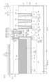
- FIG. 18 is an enlarged plan view showing an example of a third wiring unit.
- FIG. 19 is an enlarged plan view showing an example of the fourth wiring unit.
- FIG. 20 is an enlarged plan view showing a first wiring unit of a semiconductor device according to the second embodiment.
- 21 is an enlarged plan view showing a main part of the first wiring unit shown in FIG. 20.
- FIG. FIG. 22 is a plan view showing a first layout example of second layer wiring of a semiconductor device according to the third embodiment.
- FIG. 23 is a plan view showing a second layout example of the second layer wiring shown in FIG.
- FIG. 24 is an enlarged plan view showing a main part of the second layer wiring shown in FIG.
- FIG. 25 is an enlarged plan view showing a main part of the second layer wiring shown in FIG.
- FIG. 26 is an enlarged plan view showing a main part of the second layer wiring shown in FIG.
- FIG. 27 is an enlarged plan view showing a main part of the second layer wiring shown in FIG.
- FIG. 28 is a plan view showing a first modified example of the semiconductor device according to the first to third aspects.
- FIG. 29 is an enlarged plan view showing a main portion of the second layer wiring.
- FIG. 30 is a plan view showing a second modification of the semiconductor device according to the first to third aspects.
- FIG. 30 is a plan view showing a second modification of the semiconductor device according to the first to third aspects.
- FIG. 31 is a plan view showing a semiconductor device according to the fourth embodiment.
- 32 is a cross-sectional view taken along line XXXII-XXXII shown in FIG. 31.
- FIG. FIG. 33 is a plan view showing an example of the layout of the first main surface.
- FIG. 34 is an enlarged plan view showing a main portion of the first main surface.
- FIG. 35 is an enlarged plan view showing a main portion of the first main surface.
- 36 is a cross-sectional view taken along line XXXVI-XXXVI shown in FIG. 35.
- FIG. 37 is a cross-sectional view taken along line XXXVII-XXXVII shown in FIG. 35.
- FIG. 35 is a cross-sectional view taken along line XXXVII-XXXVII shown in FIG. 35.
- FIG. 38 is a cross-sectional view taken along line XXXVIII-XXXVIII shown in FIG. 35.
- FIG. 39 is a cross-sectional view taken along line XXXIX-XXXIX shown in FIG. 35.
- FIG. 40 is a plan view showing an example of the layout of the first layer wiring.
- FIG. 41 is a plan view showing an example of the layout of the second layer wiring.
- FIG. 42A is an enlarged plan view showing a first wiring unit according to the first example.
- FIG. 42B is an enlarged plan view showing the first wiring unit according to the second example.
- FIG. 42C is an enlarged plan view showing a first wiring unit according to the third example.
- FIG. 42D is an enlarged plan view showing a first wiring unit according to the fourth example.
- FIG. 42E is an enlarged plan view showing a first wiring unit according to the fifth example.
- FIG. 42F is an enlarged plan view showing a first wiring unit according to the sixth example.
- FIG. 42G is an enlarged plan view showing a first wiring unit according to the seventh example.
- FIG. 42H is an enlarged plan view showing a first wiring unit according to the eighth example.
- FIG. 42I is an enlarged plan view showing a first wiring unit according to the ninth example.
- FIG. 42J is an enlarged plan view showing a first wiring unit according to a tenth example.
- FIG. 43A is an enlarged plan view showing a second wiring unit according to the first example.
- FIG. 43B is an enlarged plan view showing the second wiring unit according to the second example.
- FIG. 43A is an enlarged plan view showing a second wiring unit according to the first example.
- FIG. 43B is an enlarged plan view showing the second wiring unit according to the second example.
- FIG. 43A is an enlarged plan view showing a
- FIG. 43C is an enlarged plan view showing a second wiring unit according to the third example.
- FIG. 44 is an enlarged plan view showing an example of a third wiring unit.
- FIG. 45 is an enlarged plan view showing an example of the fourth wiring unit.
- FIG. 46 is a plan view showing a modification of the semiconductor device according to the fourth embodiment.
- this term includes a numerical value (shape) that is equal to the numerical value (shape) of the comparison target, as well as a numerical error (shape error) within a range of ⁇ 10% based on the numerical value (shape) of the comparison target.
- shape a numerical value that is equal to the numerical value (shape) of the comparison target
- error a numerical error within a range of ⁇ 10% based on the numerical value (shape) of the comparison target.
- the conductivity type of a semiconductor is indicated using “p-type” or “n-type”, but “p-type” may also be referred to as the “first conductivity type” and “n-type” as the “second conductivity type”. Of course, “n-type” may also be referred to as the "first conductivity type” and “p-type” as the “second conductivity type”.
- P-type is a conductivity type resulting from a trivalent element
- n-type is a conductivity type resulting from a pentavalent element.
- the trivalent element is at least one of boron, aluminum, gallium, and indium.
- the pentavalent element is at least one of nitrogen, phosphorus, arsenic, antimony, and bismuth.
- FIG. 1 is a plan view showing a semiconductor device 1A according to the first embodiment.
- FIG. 2 is a cross-sectional view taken along line II-II shown in FIG. 1.
- FIG. 3 is a plan view showing an example layout of the first main surface 3.
- FIG. 4 is an enlarged plan view showing a main portion of the first main surface 3.
- FIG. 5 is an enlarged plan view showing a main portion of the first main surface 3 (a main portion different from that shown in FIG. 4).
- FIG. 6 is an enlarged plan view showing a main portion of the first main surface 3 (a main portion different from that shown in FIG. 4 and FIG. 5).
- FIG. 7 is a cross-sectional view taken along line VII-VII shown in FIG. 5.
- FIG. 8 is a cross-sectional view taken along line VIII-VIII shown in FIG. 5.
- FIG. 9 is a cross-sectional view taken along line IX-IX shown in FIG. 5.
- FIG. 10 is a cross-sectional view taken along line X-X shown in FIG. 5.
- FIG. 11 is a cross-sectional view taken along line XI-XI shown in FIG. 6.
- FIG. 12 is a cross-sectional view taken along line XII-XII shown in FIG. 6.
- FIG. 13 is a cross-sectional view taken along line XIII-XIII shown in FIG. 6.
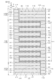
- FIG. 14 is a plan view showing an example layout of first layer wiring 74.
- FIG. 15 is a plan view showing an example layout of second layer wiring 75.
- the semiconductor device 1A is a semiconductor switching device having a lateral drain-source common type transistor structure Tr (field effect transistor) as an example of a device structure.
- the semiconductor device 1A includes a chip 2 having a hexahedral shape (specifically, a rectangular parallelepiped shape).
- the chip 2 may be referred to as a "semiconductor chip.”
- the chip 2 has a single-layer structure made of a silicon single crystal substrate (semiconductor substrate).
- the chip 2 has a first main surface 3 on one side, a second main surface 4 on the other side, and first to fourth side surfaces 5A to 5D connecting the first main surface 3 and the second main surface 4.
- the first main surface 3 and the second main surface 4 are formed in a quadrangular shape when viewed in a plan view from their normal direction Z (hereinafter simply referred to as "plan view").
- the normal direction Z is also the thickness direction of the chip 2.
- the first side 5A and the second side 5B extend in a first direction X along the first main surface 3 and face a second direction Y that intersects with the first direction X along the first main surface 3.
- the second direction Y is perpendicular to the first direction X.
- the third side 5C and the fourth side 5D extend in the second direction Y and face the first direction X.
- one side of the first direction X refers to the third side 5C side
- the other side of the first direction X refers to the fourth side 5D side.
- one side of the second direction Y refers to the first side 5A side
- the other side of the second direction Y refers to the second side 5B side.
- the semiconductor device 1A includes a plurality of active regions 6 (six in this embodiment) provided on the first main surface 3 at intervals in the first direction X.
- the plurality of active regions 6 are arranged as first to sixth active regions 6A to 6F in order from the third side surface 5C side.
- Each of the plurality of active regions 6 is a region in which a transistor structure Tr (device structure) is formed.
- the multiple active regions 6 are provided in the inner part of the first main surface 3 at a distance from the periphery of the first main surface 3 (first to fourth side surfaces 5A to 5D), and are each defined as a strip extending in the second direction Y. Specifically, the multiple active regions 6 are each defined as a polygon (a square in this embodiment) having four sides parallel to the periphery of the chip 2 in a plan view. The planar shape of the active regions 6 is arbitrary.
- the semiconductor device 1A includes an outer region 7 provided in an area outside the multiple active regions 6 on the first main surface 3.
- the outer region 7 includes multiple boundary regions 7a and one peripheral region 7b.
- the multiple boundary regions 7a are each partitioned into bands extending in the second direction Y in the area between the multiple active regions 6 adjacent in the first direction X.
- the peripheral region 7b is provided in the region between the periphery of the first main surface 3 and the multiple active regions 6, and extends in a band shape along the periphery of the first main surface 3 and the multiple active regions 6.
- the peripheral region 7b collectively surrounds the multiple active regions 6 in a plan view, and is partitioned into a polygonal ring (a square ring in this embodiment) having four sides parallel to the periphery of the chip 2.
- the peripheral region 7b is connected to the multiple boundary regions 7a.
- the semiconductor device 1A includes a p-type base layer 8 (base region) formed inside the chip 2.
- the base layer 8 may have a p-type impurity concentration of 1 ⁇ 10 13 cm ⁇ 3 or more and 1 ⁇ 10 16 cm ⁇ 3 or less.
- a base potential is applied to the base layer 8.
- the base potential may be a reference potential.
- the reference potential is a potential that serves as a reference for circuit operation.
- the reference potential may be a ground potential.
- the base layer 8 is formed over the entire thickness range of the chip 2 in the region between the first main surface 3 and the second main surface 4.
- the base layer 8 extends in a layered manner along the first main surface 3 and the second main surface 4, forming the first main surface 3, the second main surface 4 and the first to fourth side surfaces 5A to 5D.
- the chip 2 is made of a p-type semiconductor substrate (p-type semiconductor chip), and the base layer 8 is formed using the p-type chip 2.
- the base layer 8 may have a thickness of 1 ⁇ m or more and 800 ⁇ m or less.
- the thickness of the base layer 8 may have a value that belongs to at least one of the following ranges: 1 ⁇ m or more and 50 ⁇ m or less, 50 ⁇ m or more and 100 ⁇ m or less, 100 ⁇ m or more and 200 ⁇ m or less, 200 ⁇ m or more and 300 ⁇ m or less, 300 ⁇ m or more and 400 ⁇ m or less, 400 ⁇ m or more and 500 ⁇ m or less, 500 ⁇ m or more and 600 ⁇ m or less, 600 ⁇ m or more and 700 ⁇ m or less, and 700 ⁇ m or more and 800 ⁇ m or less.
- the semiconductor device 1A includes at least one (one in this embodiment) n-type drift layer 9 (drift region) formed in a surface layer portion of the first main surface 3.
- the drift layer 9 is an impurity region in which the conductivity type of the base layer 8 is replaced from p-type to n-type by ion implantation.
- the drift layer 9 may be an n-type epitaxial layer stacked on a p-type semiconductor substrate (base layer 8).
- the drift layer 9 may have an n-type impurity concentration of 1 ⁇ 10 14 cm -3 or more and 1 ⁇ 10 18 cm -3 or less.
- the drift layer 9 is formed in the multiple active regions 6 at intervals from the second main surface 4 (the bottom of the base layer 8) toward the first main surface 3, and extends in a layered manner along the first main surface 3.
- the drift layer 9 is pulled out from the multiple active regions 6 to the outer region 7, and has a portion located in the outer region 7.
- the drift layer 9 is formed in the surface layer portion of the first main surface 3 over the entire area of the first main surface 3, and is exposed from the first to fourth side surfaces 5A to 5D.
- the drift layer 9 may be formed on the surface layer of the first main surface 3 at intervals inward from the first to fourth side surfaces 5A to 5D.
- multiple drift layers 9 may be formed in a one-to-one correspondence with the multiple active regions 6.
- the multiple drift layers 9 are formed at intervals in the first direction X so as to be positioned within the multiple active regions 6, respectively, and are each formed in a band shape extending in the second direction Y.
- the depth of the drift layer 9 may be 0.1 ⁇ m or more and 10 ⁇ m or less.
- the depth of the drift layer 9 may have a value belonging to at least one of the following ranges: 0.1 ⁇ m or more and 0.25 ⁇ m or less, 0.25 ⁇ m or more and 0.5 ⁇ m or less, 0.5 ⁇ m or more and 1 ⁇ m or less, 1 ⁇ m or more and 1.5 ⁇ m or less, 1.5 ⁇ m or more and 2 ⁇ m or less, 2 ⁇ m or more and 2.5 ⁇ m or less, 2.5 ⁇ m or more and 3 ⁇ m or less, 3 ⁇ m or more and 4 ⁇ m or less, 4 ⁇ m or more and 6 ⁇ m or less, 6 ⁇ m or more and 8 ⁇ m or less, and 8 ⁇ m or more and 10 ⁇ m or less.
- the depth of the drift layer 9 is preferably 2 ⁇ m or less.
- the semiconductor device 1A includes outer insulating films 10, 11 that cover the outer surface of the chip 2.
- the outer insulating films 10, 11 include a first outer insulating film 10 and a second outer insulating film 11.
- the outer insulating films 10, 11 do not necessarily need to include both the first outer insulating film 10 and the second outer insulating film 11 at the same time, and may consist of only one of the first outer insulating film 10 and the second outer insulating film 11.
- the presence or absence of the outer insulating films 10, 11 is optional, and a configuration that does not have the outer insulating films 10, 11 may be adopted.
- the first outer insulating film 10 covers the second main surface 4 in the form of a film. In other words, the first outer insulating film 10 covers the base layer 8 exposed from the second main surface 4. In this embodiment, the first outer insulating film 10 covers the entire second main surface 4, insulating and reinforcing the chip 2 from the second main surface 4 side.
- the second outer insulating film 11 covers at least one of the first to fourth side surfaces 5A to 5D in a film-like manner. In other words, the second outer insulating film 11 covers the base layer 8 and drift layer 9 exposed from at least one of the first to fourth side surfaces 5A to 5D. In this embodiment, the second outer insulating film 11 covers all of the first to fourth side surfaces 5A to 5D, insulating and reinforcing the chip 2 from the first to fourth side surfaces 5A to 5D sides.
- the second outer insulating film 11 is continuous with the first outer insulating film 10 at the periphery of the second main surface 4.
- the outer insulating films 10, 11 may have a single-layer structure or a laminated structure including either or both of an inorganic insulating film and an organic insulating film.
- the outer insulating films 10, 11 having a laminated structure may include an inorganic insulating film and an organic insulating film laminated in this order from the chip 2 side.
- the inorganic insulating film may include at least one of a silicon oxide film, a silicon nitride film, and a silicon oxynitride film.
- the organic insulating film may include at least one of a polyimide, a polyamide, a polybenzoxazole, and an epoxy resin.
- the semiconductor device 1A includes a plurality of transistor structures Tr formed in a plurality of active regions 6 on the first main surface 3. The configuration of the plurality of transistor structures Tr will be specifically described below.
- the semiconductor device 1A includes a plurality of trench electrode type gate structures 12 (control ends) formed on the first main surface 3 in each active region 6.
- the gate structures 12 may be referred to as "trench gate structures.”
- a gate potential (gate signal) is applied to the plurality of gate structures 12 as a control potential.
- the multiple gate structures 12 are formed in stripes extending in the first direction X in each active region 6, and are arranged at intervals in the second direction Y. In other words, the multiple gate structures 12 are arranged in stripes extending in the first direction X.
- Each of the multiple gate structures 12 has a first end on one side of the first direction X and a second end on the other side of the first direction X. The first end and second end are drawn out from the active region 6 to the outer region 7.
- first ends of the multiple gate structures 12 are drawn out to the peripheral region 7b, and second ends of the multiple gate structures 12 are drawn out to the boundary region 7a.
- first ends of the multiple gate structures 12 are drawn out to one boundary region 7a, and second ends of the multiple gate structures 12 are drawn out to the other boundary region 7a.
- first ends of the multiple gate structures 12 are drawn out to the boundary region 7a, and second ends of the multiple gate structures 12 are drawn out to the peripheral region 7b.
- the multiple gate structures 12 face each other in the first direction X.
- the first ends of the multiple gate structures 12 arranged in the other active region 6 face the second ends of the multiple gate structures 12 arranged in the one active region 6 in a one-to-one correspondence.
- the multiple gate structures 12 are located within the drift layer 9 in a cross-sectional view. Specifically, the multiple gate structures 12 are formed at intervals on the first main surface 3 side with respect to the depth position of the bottom of the drift layer 9, and have side walls and a bottom wall located within the drift layer 9.
- the multiple gate structures 12 may be formed in a tapered shape in which the opening width narrows toward the bottom wall in a cross-sectional view.
- the multiple gate structures 12 may penetrate the bottom of the drift layer 9 to reach the base layer 8. That is, the multiple gate structures 12 may have a portion (side wall) located in the drift layer 9 and a portion (bottom wall) located in the base layer 8.
- the bottom wall of the multiple gate structures 12 preferably has a flat portion extending approximately parallel to the first main surface 3.
- the bottom wall of the multiple gate structures 12 may be curved in an arc shape toward the second main surface 4.
- the spacing between the multiple gate structures 12 may be 0.1 ⁇ m or more and 5 ⁇ m or less.
- the spacing between the gate structures 12 may have a value that falls within at least one of the following ranges: 0.1 ⁇ m or more and 0.5 ⁇ m or less, 0.5 ⁇ m or more and 1 ⁇ m or less, 1 ⁇ m or more and 1.5 ⁇ m or less, 1.5 ⁇ m or more and 2 ⁇ m or less, 2 ⁇ m or more and 2.5 ⁇ m or less, 2.5 ⁇ m or more and 3 ⁇ m or less, 3 ⁇ m or more and 3.5 ⁇ m or less, 3.5 ⁇ m or more and 4 ⁇ m or less, 4 ⁇ m or more and 4.5 ⁇ m or less, and 4.5 ⁇ m or more and 5 ⁇ m or less.
- the spacing between the gate structures 12 is preferably 3 ⁇ m or less.
- the width of the gate structure 12 may be 0.1 ⁇ m or more and 5 ⁇ m or less.
- the width of the gate structure 12 may have a value that belongs to at least one of the following ranges: 0.1 ⁇ m or more and 0.5 ⁇ m or less, 0.5 ⁇ m or more and 1 ⁇ m or less, 1 ⁇ m or more and 1.5 ⁇ m or less, 1.5 ⁇ m or more and 2 ⁇ m or less, 2 ⁇ m or more and 2.5 ⁇ m or less, 2.5 ⁇ m or more and 3 ⁇ m or less, 3 ⁇ m or more and 3.5 ⁇ m or less, 3.5 ⁇ m or more and 4 ⁇ m or less, 4 ⁇ m or more and 4.5 ⁇ m or less, and 4.5 ⁇ m or more and 5 ⁇ m or less.
- the width of the gate structure 12 is preferably 3 ⁇ m or less.
- the depth of the gate structure 12 may be 0.1 ⁇ m or more and 10 ⁇ m or less.
- the depth of the gate structure 12 may have a value belonging to at least one of the following ranges: 0.1 ⁇ m or more and 0.25 ⁇ m or less, 0.25 ⁇ m or more and 0.5 ⁇ m or less, 0.5 ⁇ m or more and 1 ⁇ m or less, 1 ⁇ m or more and 1.5 ⁇ m or less, 1.5 ⁇ m or more and 2 ⁇ m or less, 2 ⁇ m or more and 2.5 ⁇ m or less, 2.5 ⁇ m or more and 3 ⁇ m or less, 3 ⁇ m or more and 4 ⁇ m or less, 4 ⁇ m or more and 6 ⁇ m or less, 6 ⁇ m or more and 8 ⁇ m or less, and 8 ⁇ m or more and 10 ⁇ m or less.
- the depth of the gate structure 12 is preferably 3 ⁇ m or less.
- the gate structure 12 includes a trench 13, an insulating film 14, a buried electrode 15, and a buried insulator 16.
- the trench 13 may be referred to as a "gate trench”
- the insulating film 14 may be referred to as a “gate insulating film”
- the buried electrode 15 may be referred to as a "gate electrode”.
- the trench 13 is dug down from the first main surface 3 toward the second main surface 4, and defines the side walls and bottom wall of the gate structure 12.
- the insulating film 14 covers the wall surface of the trench 13 in a film-like manner.
- the insulating film 14 may include at least one of a silicon oxide film, a silicon nitride film, and a silicon oxynitride film. It is preferable that the insulating film 14 has a single-layer structure. It is preferable that the insulating film 14 includes a silicon oxide film made of an oxide of the chip 2.
- the buried electrode 15 is buried in the trench 13 via the insulating film 14.
- the buried electrode 15 may include conductive polysilicon.
- the buried electrode 15 includes a buried portion 15a and at least one (in this embodiment, multiple) drawn-out portion 15b.
- the buried portion 15a is buried in the bottom wall side of the trench 13 at a distance from the first main surface 3 to the bottom wall side of the trench 13 in the active region 6.
- the buried portion 15a is buried at a distance from the middle part of the trench 13 to the bottom wall side of the trench 13, and preferably has an electrode surface located closer to the bottom wall side than the middle part of the trench 13.
- the multiple pull-out portions 15b include a pull-out portion 15b located at a first end of the trench 13 in the outer region 7, and a pull-out portion 15b located at a second end of the trench 13 in the outer region 7.
- the multiple pull-out portions 15b are pulled out from the bottom wall side (buried portion 15a side) of the trench 13 to the opening side of the trench 13.
- the multiple pull-out portions 15b, together with the buried portion 15a, define an electrode recess 17 on the opening side of the trench 13.
- the electrode recess 17 extends in a band shape in the first direction X along the trench 13.
- the multiple drawers 15b have electrode surfaces located near the first main surface 3.
- the electrode surfaces of the drawers 15b may be formed flush with the first main surface 3.
- the electrode surfaces of the drawers 15b may be located on the bottom wall side of the trench 13 relative to the first main surface 3.
- the electrode surfaces of the drawers 15b may protrude above the first main surface 3.
- the buried insulator 16 is buried in the opening side of the trench 13. Specifically, the buried insulator 16 is buried in the electrode recess 17 and covers the buried portion 15a in the trench 13.
- the buried insulator 16 may be buried in the trench 13 with the insulating film 14 sandwiched therebetween.
- the buried insulator 16 may be buried in the trench 13 without the insulating film 14 interposed therebetween so as to directly cover the sidewall of the trench 13.
- the buried insulator 16 extends in a band shape in the first direction X in a plan view.
- the buried insulator 16 is provided as a field insulator that relaxes the electric field for the trench 13. It is preferable that the cross-sectional area of the buried insulator 16 is larger than the cross-sectional area of the buried portion 15a.
- the embedded insulator 16 has an insulating surface located near the first main surface 3.
- the insulating surface may be formed flush with the first main surface 3.
- the insulating surface may be located on the bottom wall side of the trench 13 relative to the first main surface 3.
- the insulating surface may protrude above the first main surface 3.
- the buried insulator 16 may contain at least one of silicon oxide, silicon nitride, and silicon oxynitride.
- the buried insulator 16 may have a single layer structure.
- the buried insulator 16 may be formed of the same insulating material as the insulating film 14. In this case, the buried insulator 16 is made of a vapor deposited by a CVD (Chemical Vapor Deposition) method or the like, and preferably has a density different from that of the insulating film 14.
- CVD Chemical Vapor Deposition
- the semiconductor device 1A includes a plurality of gate units GU1, GU2 in each active region 6.
- the plurality of gate units GU1, GU2 includes a plurality of first gate units GU1 and a plurality of second gate units GU2.
- the multiple first gate units GU1 are each composed of at least two (two in this embodiment) gate structures 12 adjacent to each other in the second direction Y in each active region 6.
- the multiple first gate units GU1 are arranged alternately with at least two (two in this embodiment) gate structures 12 in the second direction Y in each active region 6.
- the multiple first gate units GU1 face each other in the first direction X.
- the multiple first gate units GU1 arranged in the other active region 6 face the multiple first gate units GU1 arranged in the one active region 6 in a one-to-one correspondence.
- the second gate units GU2 are each composed of at least two (two in this embodiment) gate structures 12 other than the gate structures 12 constituting the first gate units GU1 among the gate structures 12 in each active region 6.
- the second gate units GU2 are each composed of at least two gate structures 12 adjacent to each other in the second direction Y in each active region 6.
- the second gate units GU2 are arranged alternately with the first gate units GU1 in the second direction Y in each active region 6.
- the multiple second gate units GU2 face each other in the first direction X.
- the multiple second gate units GU2 arranged in the other active region 6 face the multiple second gate units GU2 arranged in the one active region 6 in a one-to-one correspondence.
- the semiconductor device 1A includes a plurality of unit spaces US that are partitioned into regions between a plurality of first gate units GU1 and a plurality of second gate units GU2 that are adjacent to each other in the second direction Y in each active region 6.
- Each unit space US is partitioned into a region between one gate structure 12 of the first gate unit GU1 and one gate structure 12 of the second gate unit GU2, and includes a drift layer 9.
- the semiconductor device 1A includes a plurality of trench electrode type connection structures 21, 22 formed in the outer region 7 of the first main surface 3.
- the plurality of connection structures 21, 22 connect at least two gate structures 12 adjacent to each other in the second direction Y.
- a gate potential is applied to the plurality of connection structures 21, 22.
- the connection structures 21, 22 may be referred to as "gate connection structures.”
- the multiple connection structures 21, 22 are connected to the first and second ends of the multiple gate structures 12 in the corresponding gate units GU1, GU2, respectively.
- the multiple connection structures 21, 22 include multiple first connection structures 21 arranged on the first end side of the multiple gate structures 12, and multiple second connection structures 22 arranged on the second end side of the multiple gate structures 12.
- the multiple first connection structures 21 are each formed in a band extending in the second direction Y, and are arranged at intervals in the second direction Y.
- the multiple first connection structures 21 are arranged in a line in the second direction Y.
- the multiple first connection structures 21 are each connected to the first ends of the multiple gate structures 12 to be unitized (grouped). In this embodiment, the multiple first connection structures 21 each connect the first ends of a pair of gate structures 12 adjacent in the second direction Y.
- the multiple second connection structures 22 are each formed in a band extending in the second direction Y, and are arranged at intervals in the second direction Y.
- the multiple second connection structures 22 are arranged in a line in the second direction Y.
- the multiple second connection structures 22 are each connected to the second ends of the multiple gate structures 12 that are unitized (grouped) by the first connection structure 21.
- the multiple second connection structures 22 are each connected to the second ends of a pair of gate structures 12 adjacent to each other in the second direction Y.
- the multiple first connection structures 21 are respectively connected to the first ends of the multiple gate structures 12 adjacent in the second direction Y in the peripheral region 7b, and the multiple second connection structures 22 are respectively connected to the second ends of the multiple gate structures 12 unitized by the first connection structures 21 in the boundary region 7a.
- the multiple first connection structures 21 are respectively connected to the first ends of the multiple gate structures 12 adjacent in the second direction Y in one boundary region 7a
- the multiple second connection structures 22 are respectively connected to the second ends of the multiple gate structures 12 unitized by the first connection structures 21 in the other boundary region 7a.
- the multiple first connection structures 21 are respectively connected to first ends of multiple gate structures 12 adjacent in the second direction Y in the boundary region 7a
- the multiple second connection structures 22 are respectively connected to second ends of multiple gate structures 12 unitized by the first connection structures 21 in the peripheral region 7b.
- the multiple second connection structures 22 are formed at intervals in the first direction X from the multiple first connection structures 21, and each face the multiple first connection structures 21 in the first direction X in a one-to-one correspondence.
- the multiple connection structures 21, 22 are located within the drift layer 9 in a cross-sectional view. Specifically, the multiple connection structures 21, 22 are formed at intervals on the first main surface 3 side with respect to the depth position of the bottom of the drift layer 9, and have side walls and a bottom wall located within the drift layer 9.
- the multiple connection structures 21, 22 may be formed in a tapered shape in which the opening width narrows toward the bottom wall in a cross-sectional view.
- the multiple connection structures 21, 22 may penetrate the bottom of the drift layer 9 to reach the base layer 8 and have a bottom wall located within the base layer 8. That is, the multiple connection structures 21, 22 may have a portion (side wall) located within the drift layer 9 and a portion (bottom wall) located within the base layer 8.
- the bottom walls of the multiple connection structures 21, 22 preferably have a flat portion extending approximately parallel to the first main surface 3. Of course, the bottom walls of the multiple connection structures 21, 22 may be curved in an arc toward the second main surface 4.
- the width of the connection structures 21, 22 is greater than the width of the gate structure 12 in this embodiment.
- the width of the connection structures 21, 22 may be approximately equal to the width of the gate structure 12.
- the width of the connection structures 21, 22 may be less than the width of the gate structure 12.
- the width of the connection structures 21, 22 may be 0.1 ⁇ m or more and 5 ⁇ m or less.
- the width of the connection structures 21, 22 may have a value that belongs to at least one of the following ranges: 0.1 ⁇ m or more and 0.5 ⁇ m or less, 0.5 ⁇ m or more and 1 ⁇ m or less, 1 ⁇ m or more and 1.5 ⁇ m or less, 1.5 ⁇ m or more and 2 ⁇ m or less, 2 ⁇ m or more and 2.5 ⁇ m or less, 2.5 ⁇ m or more and 3 ⁇ m or less, 3 ⁇ m or more and 3.5 ⁇ m or less, 3.5 ⁇ m or more and 4 ⁇ m or less, 4 ⁇ m or more and 4.5 ⁇ m or less, and 4.5 ⁇ m or more and 5 ⁇ m or less.
- the depth of the connection structures 21, 22 is greater than the depth of the gate structure 12 in this embodiment.
- the depth of the connection structures 21, 22 may be approximately equal to the depth of the gate structure 12.
- the depth of the connection structures 21, 22 may be less than the depth of the gate structure 12.
- the depth of the connection structures 21, 22 may be 0.1 ⁇ m or more and 10 ⁇ m or less.
- the depth of the connection structures 21, 22 may have a value that belongs to at least one of the following ranges: 0.1 ⁇ m or more and 0.25 ⁇ m or less, 0.25 ⁇ m or more and 0.5 ⁇ m or less, 0.5 ⁇ m or more and 1 ⁇ m or less, 1 ⁇ m or more and 1.5 ⁇ m or less, 1.5 ⁇ m or more and 2 ⁇ m or less, 2 ⁇ m or more and 2.5 ⁇ m or less, 2.5 ⁇ m or more and 3 ⁇ m or less, 3 ⁇ m or more and 4 ⁇ m or less, 4 ⁇ m or more and 6 ⁇ m or less, 6 ⁇ m or more and 8 ⁇ m or less, and 8 ⁇ m or more and 10 ⁇ m or less.
- connection structures 21, 22 include a connection trench 23, a connection insulating film 24, and a connection electrode 25.
- the connection trench 23 is dug from the first main surface 3 toward the second main surface 4, and defines the side walls and bottom walls of the connection structures 21, 22.
- the connection trench 23 is connected to multiple trenches 13 adjacent to each other in the second direction Y.
- connection insulating film 24 covers the wall surface of the connection trench 23 in a film-like manner.
- the connection insulating film 24 is connected to the insulating film 14 and the buried insulator 16 at the communicating portion between the trench 13 and the connection trench 23.
- the connection insulating film 24 may include at least one of a silicon oxide film, a silicon nitride film, and a silicon oxynitride film.
- the connection insulating film 24 preferably has a single-layer structure.
- the connection insulating film 24 preferably includes a silicon oxide film made of an oxide of the chip 2.
- the connection insulating film 24 is preferably formed of the same insulating material as the insulating film 14.
- connection electrode 25 is embedded in the connection trench 23 via the connection insulating film 24.
- the connection electrode 25 may contain conductive polysilicon.
- the connection electrode 25 is formed in a band shape extending in the second direction Y in a plan view, and is connected to the embedded electrode 15 at the communicating portion between the trench 13 and the connection trench 23.
- connection electrode 25 may be regarded as the portion of the buried electrode 15 (drawing portion 15b) that is drawn into the connection trench 23.
- the connection portion of the buried electrode 15 and the connection electrode 25 may be regarded as one component of the gate structure 12, or as one component of the connection structures 21 and 22.
- the connection electrode 25 has an electrode surface located near the first main surface 3.
- the electrode surface of the connection electrode 25 may be formed flush with the first main surface 3.
- the electrode surface of the connection electrode 25 may be located on the bottom wall side of the connection trench 23 with respect to the first main surface 3.
- the electrode surface of the connection electrode 25 may protrude above the first main surface 3. It is preferable that the plane area of the electrode surface of the connection electrode 25 is larger than the plane area of the electrode surface of the embedded portion 15a.
- the semiconductor device 1A includes a plurality of mesas 26, 27 that are each partitioned into a plurality of active regions 6 on the first main surface 3.
- the plurality of mesas 26, 27 are each partitioned by a plurality of gate units GU1, GU2. That is, each mesa 26, 27 is composed of a portion surrounded by a plurality of gate structures 12 and a plurality of connection structures 21, 22.
- the plurality of mesas 26, 27 each extend in a band shape in the first direction X, and are partitioned at intervals in the second direction Y. That is, the plurality of mesas 26, 27 are partitioned in stripes extending in the first direction X.
- the multiple mesa portions 26, 27 include multiple first mesa portions 26 and multiple second mesa portions 27.
- the multiple first mesa portions 26 are each partitioned by multiple first gate units GU1, and are regions (first application terminals) to which a first drain-source potential is applied as a first potential (high potential).
- the multiple first mesa portions 26 face each other in the first direction X.
- the multiple first mesa portions 26 defined in the other active region 6 face the multiple first mesa portions 26 defined in the one active region 6 in a one-to-one correspondence.
- the multiple second mesa portions 27 are each defined by multiple second gate units GU2, and are regions (second application terminals) to which a second drain-source potential is applied as a second potential (low potential) different from the first potential.
- the multiple second mesa portions 27 are defined alternately with the multiple first mesa portions 26 in the second direction Y via multiple unit spaces US.
- the second drain-source potential may be the same potential as the base potential, or may be a potential different from the base potential.
- the multiple second mesa portions 27 face each other in the first direction X.
- the multiple second mesa portions 27 defined in the other active region 6 face the multiple second mesa portions 27 defined in the one active region 6 in a one-to-one correspondence.
- the semiconductor device 1A includes a plurality of n-type drain source regions 28, 29 formed in a surface layer portion of the first main surface 3 (drift layer 9) in each active region 6.
- the plurality of drain source regions 28, 29 are formed in a plurality of mesa portions 26, 27. That is, the plurality of drain source regions 28, 29 are formed in regions between a plurality of gate structures 12 in the corresponding gate units GU1, GU2, respectively.
- the plurality of drain source regions 28, 29 have an n-type impurity concentration higher than the n-type impurity concentration of the drift layer 9.
- the n-type impurity concentration of the plurality of drain source regions 28, 29 may be 1 ⁇ 10 16 cm ⁇ 3 or more and 1 ⁇ 10 21 cm ⁇ 3 or less.
- the multiple drain source regions 28, 29 include multiple first drain source regions 28 and multiple second drain source regions 29.
- the multiple first drain source regions 28 are regions (first application ends) to which a first drain source potential is applied, and are formed in a band shape extending in the first direction X in the multiple first mesa portions 26.
- the multiple first drain source regions 28 face each other in the first direction X.
- the multiple first drain source regions 28 arranged in the other active region 6 face the multiple first drain source regions 28 arranged in the one active region 6 in a one-to-one correspondence.
- the second drain source regions 29 are regions (second application ends) to which the second drain source potential is applied, and are formed in stripes extending in the first direction X in the second mesa portions 27. In other words, the second drain source regions 29 are formed alternately with the first drain source regions 28 in the second direction Y. The drain source regions 28, 29 are also arranged in stripes extending in the first direction X.
- the multiple second drain source regions 29 face each other in the first direction X.
- the multiple second drain source regions 29 arranged in the other active region 6 face the multiple second drain source regions 29 arranged in the one active region 6 in a one-to-one correspondence.
- the configuration of one drain source region 28, 29 will be described below.
- the drain source region 28, 29 is formed at a distance from the bottom walls of the multiple gate structures 12 toward the first main surface 3, and faces the base layer 8 across a part of the drift layer 9.
- the drain source region 28, 29 is formed at a distance from the depth position of the electrode surfaces of the multiple buried electrodes 15 toward the first main surface 3, and faces the multiple buried insulators 16 in the horizontal direction along the first main surface 3.
- drain source regions 28, 29 may be in contact with multiple gate structures 12. In other words, the drain source regions 28, 29 may be in contact with the portions of the multiple gate structures 12 where the buried insulator 16 is disposed.
- the drain source regions 28, 29 are formed at intervals in the first direction X from the first and second ends of the multiple gate structures 12, and are not in contact with the portions of the multiple gate structures 12 where the pull-out portions 15b are located. In other words, the drain source regions 28, 29 are formed at intervals in the first direction X from the multiple connection structures 21, 22 located on both sides. This configuration is effective in suppressing a decrease in breakdown voltage caused by a voltage drop between the ends of the gate structure 12 (connection structures 21, 22) and the drain source regions 28, 29.
- the drain source regions 28, 29 are preferably formed with a region spacing of 0.1 ⁇ m or more and 2 ⁇ m or less from the end of the gate structure 12 (connection structures 21, 22).
- the region spacing may have a value that belongs to at least one of the following ranges: 0.1 ⁇ m or more and 0.25 ⁇ m or less, 0.25 ⁇ m or more and 0.5 ⁇ m or less, 0.5 ⁇ m or more and 0.75 ⁇ m or less, 0.75 ⁇ m or more and 1 ⁇ m or less, 1 ⁇ m or more and 1.25 ⁇ m or less, 1.25 ⁇ m or more and 1.5 ⁇ m or less, 1.5 ⁇ m or more and 1.75 ⁇ m or less, and 1.75 ⁇ m or more and 2 ⁇ m or less.
- the semiconductor device 1A includes a plurality of trench electrode type isolation structures 31, 32 formed in each active region 6 on the first main surface 3. A gate potential is applied to the plurality of isolation structures 31, 32.
- the isolation structures 31, 32 may be referred to as "gate isolation structures.”
- the plurality of isolation structures 31, 32 each connects a plurality of gate structures 12 adjacent to each other in the second direction Y in the corresponding gate units GU1, GU2.
- the multiple isolation structures 31, 32 are disposed in the regions between the ends of the multiple gate structures 12 and the multiple drain source regions 28, 29, respectively, and physically and electrically isolate the multiple drain source regions 28, 29 from the ends of the multiple gate structures 12. In other words, the multiple isolation structures 31, 32 physically and electrically isolate the multiple drain source regions 28, 29 from the multiple connection structures 21, 22.
- the multiple isolation structures 31, 32 define the boundary between the active region 6 and the outer region 7 on the first main surface 3, while at the same time increasing the creepage distance between the end of the gate structure 12 (connection structures 21, 22) and the drain-source regions 28, 29.
- the multiple isolation structures 31, 32 include multiple first isolation structures 31 arranged on the first end side, and multiple second isolation structures 32 arranged on the second end side.
- the multiple first isolation structures 31 are arranged at intervals from the multiple first ends (multiple first connection structures 21) toward the drain source regions 28, 29.
- the multiple first isolation structures 31 each extend in a strip shape in the second direction Y, and are each connected to the multiple gate structures 12 adjacent in the second direction Y.
- the multiple first isolation structures 31 are arranged in a line in the second direction Y.
- the multiple first isolation structures 31 may be connected to the drain source regions 28, 29.
- the multiple second isolation structures 32 are arranged at intervals from the multiple second ends (multiple second connection structures 22) toward the drain source regions 28, 29.
- the multiple second isolation structures 32 each extend in a strip shape in the second direction Y, and are each connected to the multiple gate structures 12 adjacent in the second direction Y.
- the multiple second isolation structures 32 are arranged in a line in the second direction Y.
- the multiple second isolation structures 32 may be connected to the drain source regions 28, 29.
- the multiple isolation structures 31, 32 are located within the drift layer 9 in a cross-sectional view. Specifically, the multiple isolation structures 31, 32 are formed at intervals on the first main surface 3 side with respect to the depth position of the bottom of the drift layer 9, and have side walls and a bottom wall located within the drift layer 9.
- the multiple isolation structures 31, 32 may be formed in a tapered shape in which the opening width narrows toward the bottom wall in a cross-sectional view.
- the multiple isolation structures 31, 32 may penetrate the bottom of the drift layer 9 to reach the base layer 8. That is, the multiple isolation structures 31, 32 may have a portion (side wall) located in the drift layer 9 and a portion (bottom wall) located in the base layer 8.
- the bottom walls of the multiple isolation structures 31, 32 preferably have a flat portion extending approximately parallel to the first main surface 3.
- the bottom walls of the multiple isolation structures 31, 32 may be curved in an arc shape toward the second main surface 4.
- the width of the isolation structures 31, 32 in this embodiment, is less than the width of the connection structures 21, 22.
- the width of the isolation structures 31, 32 may be approximately equal to the width of the connection structures 21, 22.
- the width of the isolation structures 31, 32 may be greater than the width of the connection structures 21, 22.
- the width of the isolation structures 31, 32 may be approximately equal to the width of the gate structure 12.
- the width of the isolation structures 31, 32 may be greater than the width of the gate structure 12.
- the width of the isolation structures 31, 32 may be less than the width of the gate structure 12.
- the width of the isolation structures 31, 32 may be 0.1 ⁇ m or more and 5 ⁇ m or less.
- the width of the isolation structures 31, 32 may have a value that belongs to at least one of the following ranges: 0.1 ⁇ m or more and 0.5 ⁇ m or less, 0.5 ⁇ m or more and 1 ⁇ m or less, 1 ⁇ m or more and 1.5 ⁇ m or less, 1.5 ⁇ m or more and 2 ⁇ m or less, 2 ⁇ m or more and 2.5 ⁇ m or less, 2.5 ⁇ m or more and 3 ⁇ m or less, 3 ⁇ m or more and 3.5 ⁇ m or less, 3.5 ⁇ m or more and 4 ⁇ m or less, 4 ⁇ m or more and 4.5 ⁇ m or less, and 4.5 ⁇ m or more and 5 ⁇ m or less.
- the depth of the isolation structures 31, 32 is less than the depth of the connection structures 21, 22.
- the depth of the isolation structures 31, 32 may be approximately equal to the depth of the connection structures 21, 22.
- the depth of the isolation structures 31, 32 may be greater than the depth of the connection structures 21, 22.
- the depth of the isolation structures 31, 32 may be approximately equal to the depth of the gate structure 12.
- the depth of the isolation structures 31, 32 may be greater than the depth of the gate structure 12.
- the depth of the isolation structures 31, 32 may be less than the depth of the gate structure 12.
- the isolation structures 31, 32 may be formed at a distance from the depth position of the middle part of the gate structure 12 toward the first main surface 3.
- the depth of the isolation structures 31, 32 may be 0.1 ⁇ m or more and 10 ⁇ m or less.
- the depth of the isolation structures 31, 32 may have a value that belongs to at least one of the following ranges: 0.1 ⁇ m or more and 0.25 ⁇ m or less, 0.25 ⁇ m or more and 0.5 ⁇ m or less, 0.5 ⁇ m or more and 1 ⁇ m or less, 1 ⁇ m or more and 1.5 ⁇ m or less, 1.5 ⁇ m or more and 2 ⁇ m or less, 2 ⁇ m or more and 2.5 ⁇ m or less, 2.5 ⁇ m or more and 3 ⁇ m or less, 3 ⁇ m or more and 4 ⁇ m or less, 4 ⁇ m or more and 6 ⁇ m or less, 6 ⁇ m or more and 8 ⁇ m or less, and 8 ⁇ m or more and 10 ⁇ m or less.
- the isolation structures 31, 32 include an isolation trench 33, an isolation insulating film 34, an isolation electrode 35, and an isolation buried insulator 36.
- the isolation trench 33 is dug from the first main surface 3 toward the second main surface 4, and defines the side walls and bottom walls of the isolation structures 31, 32.
- the isolation trench 33 is connected to multiple trenches 13 adjacent to each other in the second direction Y.
- the isolation insulating film 34 covers the wall surface of the isolation trench 33 in a film-like manner.
- the isolation insulating film 34 is connected to the insulating film 14 and the buried insulator 16 at the communicating portion between the trench 13 and the isolation trench 33.
- the isolation insulating film 34 may be regarded as a portion of the insulating film 14 that is drawn into the isolation trench 33.
- the connection portion between the insulating film 14 and the isolation insulating film 34 may be regarded as one component of the gate structure 12, or may be regarded as one component of the isolation structures 31 and 32.
- the isolation insulating film 34 may include at least one of a silicon oxide film, a silicon nitride film, and a silicon oxynitride film. It is preferable that the isolation insulating film 34 has a single-layer structure. It is preferable that the isolation insulating film 34 includes a silicon oxide film made of an oxide of the chip 2. It is preferable that the isolation insulating film 34 is formed of the same insulating material as the insulating film 14.
- the separation electrode 35 is embedded in the separation trench 33 via the separation insulating film 34.
- the separation electrode 35 may include conductive polysilicon.
- the separation electrode 35 is embedded in the bottom wall side of the trench 13 at a distance from the first main surface 3 to the bottom wall side of the separation trench 33. It is preferable that the separation electrode 35 is embedded at a distance from the middle part of the separation trench 33 to the bottom wall side of the separation trench 33, and has an electrode surface located closer to the bottom wall side than the middle part of the separation trench 33.
- the separation electrode 35 is connected to the buried portion 15a at the communicating portion between the trench 13 and the separation trench 33.
- the separation electrode 35 may be regarded as the portion of the buried electrode 15 (buried portion 15a) that is pulled out into the separation trench 33.
- the connection portion of the buried electrode 15 and the separation electrode 35 may be regarded as one component of the gate structure 12, or may be regarded as one component of the separation structures 31 and 32.
- the electrode surface of the separation electrode 35 is located on the bottom wall side of the separation trench 33 relative to the electrode surface of the extraction portion 15b of the buried electrode 15. It is preferable that the electrode surface of the separation electrode 35 is located at a depth position approximately equal to that of the electrode surface of the buried portion 15a.
- the buried isolation insulator 36 is buried in the opening side of the isolation trench 33.
- the buried isolation insulator 36 may be buried in the isolation trench 33 with the isolation insulating film 34 in between.
- the buried isolation insulator 36 may be buried in the isolation trench 33 without the isolation insulating film 34 in between so as to directly cover the sidewall of the isolation trench 33.
- the isolated buried insulator 36 extends in a band shape in the second direction Y in a plan view.
- the isolated buried insulator 36 is connected to the buried insulator 16 at the communicating portion between the trench 13 and the isolation trench 33.
- the isolated buried insulator 36 is provided as a field insulator that reduces the electric field to the isolation trench 33. It is preferable that the cross-sectional area of the isolated buried insulator 36 is larger than the cross-sectional area of the isolation electrode 35.
- the isolation buried insulator 36 has an insulating surface located near the first main surface 3.
- the insulating surface may be formed flush with the first main surface 3.
- the insulating surface may be located on the bottom wall side of the isolation trench 33 relative to the first main surface 3.
- the insulating surface may protrude above the first main surface 3.
- the isolated buried insulator 36 may contain at least one of silicon oxide, silicon nitride, and silicon oxynitride.
- the isolated buried insulator 36 may have a single layer structure.
- the isolated buried insulator 36 may be formed of the same insulating material as the isolated insulating film 34.
- the isolated buried insulator 36 is preferably made of a deposition material deposited by a CVD method or the like, and has a density different from that of the isolated insulating film 34.
- the isolated buried insulator 36 is preferably formed of the same insulating material as the buried insulator 16.
- the isolation structures 31 and 32 may be of a trench insulation type instead of a trench electrode type.
- an insulator silicon oxide, silicon nitride, silicon oxynitride, etc.
- the isolation insulating film 34 may be omitted.
- the floating regions 37 may include high-concentration regions in the surface portion of the drift layer 9 that have a higher n-type impurity concentration than the n-type impurity concentration of the drift layer 9.
- the n-type impurity concentration of the high-concentration regions may be approximately equal to the n-type impurity concentration of the drain source regions 28, 29.
- the high-concentration regions may also have a depth approximately equal to the depth of the drain source regions 28, 29.
- the number of field structures 42 may be 1, 2, 3, 4, 5, 6, 7, 8, 9, or 10.
- the number of field structures 42 is preferably 5 or less.
- the semiconductor device 1A includes three field structures 42.
- a base potential or a second drain source potential (low potential) may be applied to the multiple field structures 42.
- the multiple field structures 42 may be formed in an electrically floating state.
- the multiple field structures 42 are formed on the first main surface 3 in the peripheral region 7b at intervals from the multiple gate structures 12 (multiple connection structures 21, 22) toward the peripheral edge of the first main surface 3. It is preferable that the intervals between the multiple gate structures 12 (multiple connection structures 21, 22) and the innermost field structure 42 (closer to the active region 6) are greater than the intervals between the multiple gate structures 12. Of course, the intervals between the gate structures 12 and the field structures 42 may be equal to or less than the intervals between the multiple gate structures 12.
- the multiple field structures 42 are spaced apart from one another and each extend in a strip shape along the periphery of the first main surface 3.
- the multiple field structures 42 collectively surround the multiple active regions 6 (multiple gate structures 12) in a plan view, and are formed in a polygonal ring shape (a square ring in this embodiment) having four sides parallel to the periphery of the chip 2.
- the multiple field structures 42 may penetrate the bottom of the drift layer 9 to reach the base layer 8. That is, the multiple field structures 42 may have a portion (side wall) located in the drift layer 9 and a portion (bottom wall) located in the base layer 8.
- the bottom wall of the multiple field structures 42 preferably has a flat portion extending approximately parallel to the first main surface 3.
- the bottom wall of the multiple field structures 42 may be curved in an arc shape toward the second main surface 4.
- the spacing between the multiple field structures 42 may be approximately equal to the spacing between the multiple gate structures 12. The spacing between the multiple field structures 42 may be less than the spacing between the multiple gate structures 12. The spacing between the multiple field structures 42 may be greater than the spacing between the multiple gate structures 12.
- the spacing between the multiple field structures 42 may be 0.1 ⁇ m or more and 5 ⁇ m or less.
- the spacing between the field structures 42 may have a value that falls within at least one of the following ranges: 0.1 ⁇ m or more and 0.5 ⁇ m or less, 0.5 ⁇ m or more and 1 ⁇ m or less, 1 ⁇ m or more and 1.5 ⁇ m or less, 1.5 ⁇ m or more and 2 ⁇ m or less, 2 ⁇ m or more and 2.5 ⁇ m or less, 2.5 ⁇ m or more and 3 ⁇ m or less, 3 ⁇ m or more and 3.5 ⁇ m or less, 3.5 ⁇ m or more and 4 ⁇ m or less, 4 ⁇ m or more and 4.5 ⁇ m or less, and 4.5 ⁇ m or more and 5 ⁇ m or less.
- the width of the field structure 42 in this embodiment, is greater than the width of the gate structure 12.
- the width of the field structure 42 may be less than the width of the gate structure 12.
- the width of the field structure 42 may be approximately equal to the width of the gate structure 12.
- the width of the field structure 42 may be approximately equal to the width of the connection structures 21, 22.
- the width of the field structure 42 may be greater than the width of the connection structures 21, 22.
- the width of the field structure 42 may be less than the width of the connection structures 21, 22.
- the width of the field structure 42 may be 0.1 ⁇ m or more and 5 ⁇ m or less.
- the width of the field structure 42 may have a value that belongs to at least one of the following ranges: 0.1 ⁇ m or more and 0.5 ⁇ m or less, 0.5 ⁇ m or more and 1 ⁇ m or less, 1 ⁇ m or more and 1.5 ⁇ m or less, 1.5 ⁇ m or more and 2 ⁇ m or less, 2 ⁇ m or more and 2.5 ⁇ m or less, 2.5 ⁇ m or more and 3 ⁇ m or less, 3 ⁇ m or more and 3.5 ⁇ m or less, 3.5 ⁇ m or more and 4 ⁇ m or less, 4 ⁇ m or more and 4.5 ⁇ m or less, and 4.5 ⁇ m or more and 5 ⁇ m or less.
- the depth of the field structure 42 in this embodiment, is greater than the depth of the gate structure 12.
- the depth of the field structure 42 may be less than the depth of the gate structure 12.
- the depth of the field structure 42 may be approximately equal to the depth of the gate structure 12.
- the depth of the field structure 42 may be approximately equal to the depth of the connection structures 21, 22.
- the depth of the field structure 42 may be greater than the depth of the connection structures 21, 22.
- the depth of the field structure 42 may be less than the depth of the connection structures 21, 22.
- the configuration of one field structure 42 is described below.
- the field structure 42 includes a field trench 43, a field insulating film 44, and a field electrode 45.
- the field trench 43 is dug from the first main surface 3 toward the second main surface 4, and defines the side walls and bottom wall of the field structure 42.
- the multiple first impurity regions 51 face the buried electrode 15 across the insulating film 14 at the lower end of the corresponding gate structure 12.
- the multiple first impurity regions 51 are electrically connected to the drift layer 9 on the first main surface 3 side, and are electrically connected to the base layer 8 on the second main surface 4 side.
- the multiple first impurity regions 51 have a portion on the first main surface 3 side where the conductivity type of the drift layer 9 is replaced from n-type to p-type.
- the multiple first impurity regions 51 are each formed to be wider than the corresponding gate structure 12.
- the multiple first impurity regions 51 each include a bulge portion that protrudes in an arc shape (circular arc shape) in the horizontal direction (both sides) from the region below the gate structure 12 in a cross-sectional view.
- the bulge portion faces the sidewall of the gate structure 12 in the thickness direction of the chip 2.
- the drain source current Ids flows from the first drain source region 28 to the second drain source region 29 via the drift layer 9 and the multiple first impurity regions 51.
- the drain source current Ids passes in the second direction Y through the region below the multiple (two in this embodiment) gate structures 12 interposed between the first drain source region 28 and the second drain source region 29.
- the semiconductor device 1A includes a plurality of p-type second impurity regions 52 formed in regions along the lower ends of the plurality of connection structures 21, 22 inside the chip 2.
- the second impurity regions 52 have a p-type impurity concentration higher than the p-type impurity concentration of the base layer 8.
- the p-type impurity concentration of the second impurity regions 52 is preferably approximately equal to the p-type impurity concentration of the first impurity region 51.
- the p-type impurity concentration of the second impurity regions 52 may be 1 ⁇ 10 16 cm ⁇ 3 or more and 1 ⁇ 10 19 cm ⁇ 3 or less.
- the second impurity regions 52 are formed in a one-to-one correspondence with the lower ends of the corresponding connection structures 21, 22.
- the second impurity regions 52 have a portion covering the bottom wall and a portion covering the side wall at the lower ends of the corresponding connection structures 21, 22.
- the second impurity regions 52 extend in a band shape in the second direction Y along the corresponding connection structures 21, 22 in a plan view, and are connected to the first impurity regions 51 at both ends of the corresponding connection structures 21, 22.
- the multiple second impurity regions 52 may be formed at intervals from the bottom of the drift layer 9 toward the second main surface 4. In this case, the multiple second impurity regions 52 may face the drift layer 9 with a portion of the base layer 8 in between.
- the multiple connection structures 21, 22 are formed deeper than the multiple gate structures 12, and the multiple second impurity regions 52 are formed deeper than the multiple first impurity regions 51.
- the bottoms of the multiple second impurity regions 52 are located on the second main surface 4 side relative to the bottoms of the multiple first impurity regions 51.
- the multiple connection structures 21, 22 may be formed to a depth approximately equal to the multiple gate structures 12, and the multiple second impurity regions 52 may be formed to a depth approximately equal to the multiple first impurity regions 51.
- the second impurity regions 52 are each formed to be wider than the corresponding connection structures 21, 22.
- the second impurity regions 52 each include a bulge that protrudes in an arc shape (circular arc shape) in the horizontal direction (both sides) from the region below the connection structures 21, 22 in a cross-sectional view.
- the bulge faces the sidewalls of the connection structures 21, 22 in the thickness direction of the chip 2.
- the second impurity region 52 is formed by introducing p-type impurities into the inside of the chip 2 through the bottom wall of the connection trench 23.
- the p-type impurities can be properly introduced into the inside of the chip 2. Therefore, the second impurity region 52 is properly formed in the region along the lower end of the connection structures 21, 22.
- the semiconductor device 1A includes a plurality of p-type third impurity regions 53 formed in regions along the lower ends of the plurality of isolation structures 31, 32 inside the chip 2.
- the third impurity regions 53 have a p-type impurity concentration higher than the p-type impurity concentration of the base layer 8.
- the p-type impurity concentration of the third impurity regions 53 is preferably approximately equal to the p-type impurity concentration of the first impurity region 51.
- the p-type impurity concentration of the third impurity regions 53 may be 1 ⁇ 10 16 cm ⁇ 3 or more and 1 ⁇ 10 19 cm ⁇ 3 or less.
- the third impurity regions 53 are formed in one-to-one correspondence with the lower ends of the corresponding isolation structures 31, 32.
- the third impurity regions 53 have a portion covering the bottom wall and a portion covering the side wall at the lower ends of the corresponding isolation structures 31, 32.
- the third impurity regions 53 extend in a band shape in the second direction Y along the corresponding isolation structures 31, 32 in a plan view, and are connected to the first impurity regions 51 at both ends of the corresponding isolation structures 31, 32.
- the multiple third impurity regions 53 face the isolation electrode 35 across the isolation insulating film 34 at the lower ends of the corresponding isolation structures 31, 32.
- the multiple third impurity regions 53 are electrically connected to the drift layer 9 on the first main surface 3 side, and are electrically connected to the base layer 8 on the second main surface 4 side.
- the multiple third impurity regions 53 have a portion on the first main surface 3 side where the conductivity type of the drift layer 9 is replaced from n-type to p-type.
- the multiple third impurity regions 53 may be formed at intervals from the bottom of the drift layer 9 toward the second main surface 4. In this case, the multiple third impurity regions 53 may face the drift layer 9 with a portion of the base layer 8 in between.
- the multiple isolation structures 31, 32 are formed at a depth approximately equal to that of the multiple gate structures 12, and the multiple third impurity regions 53 are formed at a depth approximately equal to that of the multiple first impurity regions 51.
- the multiple isolation structures 31, 32 may be formed deeper than the multiple gate structures 12, and the multiple third impurity regions 53 may be formed deeper than the multiple first impurity regions 51.
- the multiple third impurity regions 53 are each formed wider than the corresponding isolation structures 31, 32.
- the multiple third impurity regions 53 each include a bulge that protrudes in an arc shape (circular arc shape) in the horizontal direction (both sides) from the region below the isolation structures 31, 32 in a cross-sectional view.
- the bulge faces the sidewalls of the isolation structures 31, 32 in the thickness direction of the chip 2.
- the third impurity region 53 is formed by introducing p-type impurities into the inside of the chip 2 through the bottom wall of the isolation trench 33.
- the p-type impurities can be properly introduced into the inside of the chip 2. Therefore, the third impurity region 53 is properly formed in the region along the lower end of the isolation structures 31, 32.
- the semiconductor device 1A includes a plurality of p-type fourth impurity regions 54 formed in regions along the lower ends of the plurality of field structures 42 inside the chip 2.
- the fourth impurity regions 54 have a p-type impurity concentration higher than the p-type impurity concentration of the base layer 8.
- the p-type impurity concentration of the fourth impurity regions 54 is preferably approximately equal to the p-type impurity concentration of the first impurity region 51.
- the p-type impurity concentration of the fourth impurity regions 54 may be 1 ⁇ 10 16 cm -3 or more and 1 ⁇ 10 19 cm -3 or less.
- the multiple fourth impurity regions 54 are formed in one-to-one correspondence with the lower ends of the corresponding field structures 42 at intervals from the first impurity region 51, the second impurity region 52, and the third impurity region 53.
- the multiple fourth impurity regions 54 have a portion covering the bottom wall and a portion covering the side wall at the lower end of the corresponding field structure 42.
- the multiple fourth impurity regions 54 extend in a band shape along the corresponding field structure 42 in a planar view. Specifically, the multiple fourth impurity regions 54 extend in a ring shape along the corresponding field structure 42 in a planar view.
- the multiple fourth impurity regions 54 face the field electrode 45 across the field insulating film 44 at the lower end of the corresponding field structure 42.
- the multiple fourth impurity regions 54 are electrically connected to the drift layer 9 on the first main surface 3 side, and are electrically connected to the base layer 8 on the second main surface 4 side.
- the multiple fourth impurity regions 54 have a portion on the first main surface 3 side where the conductivity type of the drift layer 9 is replaced from n-type to p-type.
- the multiple fourth impurity regions 54 may be formed at intervals from the bottom of the drift layer 9 toward the second main surface 4. In this case, the multiple fourth impurity regions 54 may face the drift layer 9 with a portion of the base layer 8 in between.
- the multiple field structures 42 are formed deeper than the multiple gate structures 12, and the multiple fourth impurity regions 54 are formed deeper than the multiple first impurity regions 51.
- the bottoms of the multiple fourth impurity regions 54 are located on the second main surface 4 side relative to the bottoms of the multiple first impurity regions 51.
- the multiple field structures 42 may be formed to a depth approximately equal to the multiple gate structures 12, and the multiple fourth impurity regions 54 may be formed to a depth approximately equal to the multiple first impurity regions 51.
- the multiple fourth impurity regions 54 are each formed to be wider than the corresponding field structure 42.
- the multiple fourth impurity regions 54 each include a bulge that extends in an arc shape (circular arc shape) in the horizontal direction (both sides) from the region below the field structure 42 in a cross-sectional view.
- the bulge faces the sidewall of the field structure 42 in the thickness direction of the chip 2.
- the bulging portion of one fourth impurity region 54 is connected to the bulging portion of the other fourth impurity region 54.
- the multiple fourth impurity regions 54 separate the base layer 8 and the drift layer 9 in the vertical direction in the outer region 7.
- the fourth impurity region 54 is formed by introducing p-type impurities into the interior of the chip 2 through the bottom wall of the field trench 43.
- the p-type impurities can be properly introduced into the interior of the chip 2.
- the fourth impurity region 54 is properly formed in the region along the lower end of the field structure 42.
- the semiconductor device 1A includes one or more (one in this embodiment) trench electrode type base structures 55 formed in the outer region 7 on the first main surface 3.
- the base structure 55 may be referred to as a "trench base structure.”
- a base potential is applied to the base structure 55.
- the base structure 55 includes a plurality of first base structures 55a and at least one (one in this embodiment) second base structure 55b.
- the multiple first base structures 55a are arranged in multiple boundary regions 7a, respectively.
- the multiple first base structures 55a extend in a strip shape in the second direction Y in the corresponding boundary region 7a.
- the multiple first base structures 55a each have a first end on one side of the second direction Y and a second end on the other side of the second direction Y.
- the multiple first base structures 55a may also be arranged at intervals in the second direction Y in a corresponding one of the boundary regions 7a.
- Each first base structure 55a is disposed at a distance inward from the multiple gate structures 12 adjacent to it in the first direction X, and faces the multiple gate structures 12 on both sides in the first direction X.
- each first base structure 55a is disposed in a region between the multiple first connection structures 21 and the multiple second connection structures 22 in the corresponding boundary region 7a, and faces the multiple connection structures 21, 22 on both sides in the first direction X.
- the multiple first base structures 55a separate the multiple active regions 6 (multiple gate structures 12) on both sides in the first direction X.
- the second base structure 55b is disposed in the peripheral region 7b.
- the second base structure 55b is disposed in a region between the multiple active regions 6 (multiple gate structures 12) and the innermost field structure 42, and extends in a strip along the multiple active regions 6.
- the second base structure 55b has a portion that extends in a strip in the first direction X and a portion that extends in a strip in the second direction Y in a plan view, and divides the multiple active regions 6 from multiple directions.
- the second base structure 55b is formed in a region on one side of the second direction Y, spaced apart from the first ends of the multiple first base structures 55a toward the peripheral edge of the chip 2 (toward the innermost field structure 42). In other words, the first ends of the multiple first base structures 55a are formed as open ends.
- the second base structure 55b is connected to the second ends of the multiple first base structures 55a on the other side in the second direction Y.
- the second base structure 55b connects the multiple first base structures 55a in a comb-tooth shape toward the multiple boundary regions 7a.
- the second base structure 55b is formed as an extension portion that is extended from the multiple first base structures 55a to the outer peripheral region 7b.
- the base structure 55 is located within the drift layer 9 in a cross-sectional view. Specifically, the base structure 55 is formed on the first main surface 3 side with a gap from the depth position of the bottom of the drift layer 9, and has side walls and a bottom wall located within the drift layer 9.
- the base structure 55 may be formed in a tapered shape in which the opening width narrows toward the bottom wall in a cross-sectional view.
- the bottom wall of the base structure 55 may have a flat portion extending approximately parallel to the first main surface 3.
- the bottom wall of the base structure 55 may be curved in an arc shape toward the second main surface 4 side.
- the width of the base structure 55 is preferably less than the width of the field structure 42.
- the width of the base structure 55 may be greater than the width of the field structure 42.
- the width of the base structure 55 may be approximately equal to the width of the field structure 42.
- the width of the base structure 55 is less than the width of the gate structure 12 in this embodiment.
- the width of the base structure 55 may be greater than the width of the gate structure 12.
- the width of the base structure 55 may be approximately equal to the width of the gate structure 12.
- the width of the base structure 55 may be 0.1 ⁇ m or more and 5 ⁇ m or less.
- the width of the base structure 55 may have a value that belongs to at least one of the following ranges: 0.1 ⁇ m or more and 0.5 ⁇ m or less, 0.5 ⁇ m or more and 1 ⁇ m or less, 1 ⁇ m or more and 1.5 ⁇ m or less, 1.5 ⁇ m or more and 2 ⁇ m or less, 2 ⁇ m or more and 2.5 ⁇ m or less, 2.5 ⁇ m or more and 3 ⁇ m or less, 3 ⁇ m or more and 3.5 ⁇ m or less, 3.5 ⁇ m or more and 4 ⁇ m or less, 4 ⁇ m or more and 4.5 ⁇ m or less, and 4.5 ⁇ m or more and 5 ⁇ m or less.
- the depth of the base structure 55 may be 0.1 ⁇ m or more and 10 ⁇ m or less.
- the depth of the base structure 55 may have a value that belongs to at least one of the following ranges: 0.1 ⁇ m or more and 0.25 ⁇ m or less, 0.25 ⁇ m or more and 0.5 ⁇ m or less, 0.5 ⁇ m or more and 1 ⁇ m or less, 1 ⁇ m or more and 1.5 ⁇ m or less, 1.5 ⁇ m or more and 2 ⁇ m or less, 2 ⁇ m or more and 2.5 ⁇ m or less, 2.5 ⁇ m or more and 3 ⁇ m or less, 3 ⁇ m or more and 4 ⁇ m or less, 4 ⁇ m or more and 6 ⁇ m or less, 6 ⁇ m or more and 8 ⁇ m or less, and 8 ⁇ m or more and 10 ⁇ m or less.
- the base structure 55 includes a base trench 56 and a base electrode 57.
- the base trench 56 is dug from the first main surface 3 toward the second main surface 4, and defines the side walls and bottom wall of the base structure 55.
- the base electrode 57 is embedded in the base trench 56 and is electrically connected to the chip 2 within the base trench 56.
- the base electrode 57 includes a first electrode 58 and a second electrode 59.
- the first electrode 58 covers the wall surface of the base trench 56 in the form of a film.
- the first electrode 58 may have a single-layer structure made of a Ti film or a Ti alloy film.
- the first electrode 58 may have a layered structure including a Ti film and a Ti alloy film layered in this order from the chip 2 side.
- the Ti alloy film may be a TiN film.
- the second electrode 59 is embedded in the base trench 56 via the first electrode 58 and is electrically connected to the chip 2 via the first electrode 58.
- the second electrode 59 may include at least one of W, Al, an Al alloy, Cu, and a Cu alloy.
- the Al alloy may include at least one of an AlSi alloy, an AlCu alloy, and an AlSiCu alloy.
- the silicide layer 60 may include at least one of a Ti silicide layer, a Ni silicide layer, a Co silicide layer, a Mo silicide layer, and a W silicide layer.
- the silicide layer 60 includes a Ti silicide layer.
- the p-type impurity concentration of the contact region 61 is higher than the p-type impurity concentration of the base layer 8.
- the contact region 61 may be formed by introducing a p-type impurity into the base layer 8.
- the p-type impurity concentration of the contact region 61 may be not less than 1 ⁇ 10 16 cm ⁇ 3 and not more than 1 ⁇ 10 21 cm ⁇ 3 .
- the contact regions 61 extend in a band shape along the base structure 55. Specifically, the contact regions 61 are formed in the chip 2 in the regions below the first base structures 55a and the regions below the second base structures 55b. The contact regions 61 extend in a band shape in the second direction Y along the corresponding first base structures 55a in each boundary region 7a.
- the contact region 61 extends in a band shape along the second base structure 55b in the outer peripheral region 7b.
- the contact region 61 has a portion that extends in a band shape in the first direction X along the second base structure 55b and a portion that extends in a band shape in the second direction Y.
- the contact region 61 is formed in a polygonal ring shape (a square ring shape in this embodiment) that extends along the base structure 55.
- the contact region 61 extends horizontally from the region directly below the base structure 55 and is connected to the multiple gate structures 12, the multiple connection structures 21, 22, and the innermost field structure 42.
- the contact region 61 extends in the thickness direction of the chip 2 in the thickness range between the base layer 8 and the base structure 55, and penetrates the bottom of the drift layer 9 to reach the base layer 8.
- the contact region 61 has a lower end connected to the base layer 8 and an upper end connected to the base structure 55, electrically connecting the base structure 55 to the base layer 8.
- the lower end of the contact region 61 is formed at a distance from the depth position of the bottoms of the first impurity region 51 and the fourth impurity region 54 toward the first main surface 3.
- the lower end of the contact region 61 may be located below (toward the second main surface 4) the depth position of the bottom of the first impurity region 51 and the fourth impurity region 54.
- the lower end of the contact region 61 may be curved in an arc shape (circular arc shape) toward the second main surface 4.
- the lower end of the contact region 61 may be connected to the first impurity region 51 in the portion along the gate structure 12.
- the lower end of the contact region 61 may be connected to the second impurity region 52 in the portion along the connection structures 21, 22.
- the lower end of the contact region 61 may be connected to the innermost fourth impurity region 54 in the portion along the innermost field structure 42.
- the lower end of the contact region 61 may be connected to a plurality of first impurity regions 51 in a portion along a plurality of gate structures 12 adjacent in the first direction X.
- the lower end of the contact region 61 may be connected to a plurality of second impurity regions 52 in a portion along a first connection structure 21 and a second connection structure 22 adjacent in the first direction X.
- the lower end of the contact region 61 may be connected to the first impurity region 51 and the fourth impurity region 54 in the portions along the gate structure 12 and the innermost field structure 42.
- the lower end of the contact region 61 may be connected to the second impurity region 52 and the fourth impurity region 54 in the portions along the connection structures 21, 22 and the innermost field structure 42.
- the semiconductor device 1A includes an n-type surface region 62 formed around the base structure 55 in the surface portion of the first main surface 3.
- the surface region 62 has an n-type impurity concentration higher than the n-type impurity concentration of the drift layer 9.
- the n-type impurity concentration of the surface region 62 may be higher than the n-type impurity concentration of the drain source regions 28, 29.
- the n-type impurity concentration of the surface region 62 may be lower than the n-type impurity concentration of the drain source regions 28, 29.
- the n-type impurity concentration of the surface region 62 may be 1 ⁇ 10 15 cm ⁇ 3 or more and 1 ⁇ 10 20 cm ⁇ 3 or less.
- the surface region 62 extends in a band shape along the base structure 55. Specifically, in this embodiment, the surface region 62 is formed in a region along the multiple first base structures 55a and a region along the second base structure 55b in the surface portion of the first main surface 3. The surface region 62 extends in a band shape in the second direction Y along the corresponding first base structure 55a in each boundary region 7a.
- the surface region 62 is formed in a thickness range between the first main surface 3 and the contact region 61.
- the surface region 62 is electrically connected at its upper end to the base structure 55 via the silicide layer 60, and is electrically connected at its lower end to the contact region 61.
- the surface region 62 has a bottom that curves in an arc toward the first main surface 3.
- the surface region 62 is formed so as to become gradually deeper with increasing distance from the base structure 55, and has a shallow portion formed near the base structure 55 and a deep portion formed far from the base structure 55.
- the shallow portion of the surface region 62 is formed at a distance from the bottom wall of the base structure 55 toward the first main surface 3, and is electrically connected to the side wall of the base structure 55 via the silicide layer 60.
- the deep portion of the surface region 62 is located in a region on the second main surface 4 side relative to the depth position of the bottom wall of the base structure 55.
- the deep portion of the surface region 62 is located in a region on the first main surface 3 side relative to the depth position of the bottom walls of the multiple gate structures 12 and the multiple field structures 42. It is preferable that the deep portion of the surface region 62 is located in a region on the first main surface 3 side relative to the depth position of the electrode surface of the buried electrode 15.
- the deep portion of the surface region 62 is located in a region on the first main surface 3 side relative to the depth position of the middle portion of the gate structure 12.
- the deep portion of the surface region 62 is connected to the multiple gate structures 12, the multiple connection structures 21, 22, and the innermost field structure 42.
- the surface region 62 may have an approximately constant depth.
- the surface region 62 may have a concentration gradient in which the n-type impurity concentration gradually decreases in the thickness direction.
- the n-type impurity concentration of the surface region 62 may gradually decrease from the shallow portion to the deep portion.
- the n-type impurity concentration of the deep portion is less than the n-type impurity concentration of the shallow portion.
- the n-type impurity concentration of the shallow portion may be approximately equal to the n-type impurity concentration of the multiple drain source regions 28, 29.
- the semiconductor device 1A includes an insulating interlayer film 70 that covers the first main surface 3.
- the interlayer film 70 may be called an "interlayer insulating film,” “intermediate film,” “intermediate insulating film,” etc.
- the interlayer film 70 has a layered structure that includes a first interlayer film 71 and a second interlayer film 72 that are layered in this order from the chip 2 (first main surface 3) side.
- the first interlayer film 71 is an insulating film on which wiring is arranged, and has a single-layer structure made of a single insulating film or a laminated structure including multiple insulating films.
- the first interlayer film 71 may include at least one of a silicon oxide film, a silicon nitride film, and a silicon oxynitride film.
- the first interlayer film 71 collectively covers the multiple active regions 6 and the outer region 7 on the first main surface 3 in a film (layer) shape.
- the first interlayer film 71 collectively covers the multiple gate structures 12, the multiple connection structures 21, 22, the multiple isolation structures 31, 32, the multiple drain source regions 28, 29, the multiple field structures 42, etc.
- the first interlayer film 71 may cover the outer insulating films 10, 11 on the peripheral side of the first main surface 3.
- the first interlayer film 71 may cover the first main surface 3 at a distance inward from the outer insulating films 10, 11, exposing the outer insulating films 10, 11.
- the second interlayer film 72 is an insulating film in which wiring is disposed above the first interlayer film 71, and has a single-layer structure made of a single insulating film or a layered structure including multiple insulating films.
- the second interlayer film 72 may include at least one of a silicon oxide film, a silicon nitride film, and a silicon oxynitride film.
- the second interlayer film 72 covers the first interlayer film 71 in a film (layer) shape.
- the semiconductor device 1A includes a multi-layer wiring structure 73 disposed on the chip 2 (first main surface 3).
- the multi-layer wiring structure 73 is formed by utilizing an interlayer film 70.
- the multi-layer wiring structure 73 includes a first layer wiring 74 disposed on the lower layer side of the interlayer film 70, and a second layer wiring 75 disposed on the upper layer side of the interlayer film 70.
- the first layer wiring 74 is disposed on the first interlayer film 71 and is covered by the second interlayer film 72.
- the second layer wiring 75 is disposed on the second interlayer film 72 and crosses the first layer wiring 74 in a multi-level crossing.
- the multilayer wiring structure 73 is a two-layer structure including a first layer wiring 74 and a second layer wiring 75. That is, the first layer wiring 74 is formed as the bottom wiring of the multilayer wiring structure 73, and the second layer wiring 75 is formed as the top wiring of the multilayer wiring structure 73. The second layer wiring 75 is exposed from the interlayer film 70.
- the multilayer wiring structure 73 only needs to include a first layer wiring 74 and a second layer wiring 75 that face each other in the vertical direction with a portion of the interlayer film 70 (second interlayer film 72) in between, and the number of layers in the multilayer wiring structure 73 is not limited to two. In other words, the multilayer wiring structure 73 may have a stacked structure of three or more layers. For example, if the interlayer film 70 has one or more lower interlayer films below the first interlayer film 71, the multilayer wiring structure 73 may include one or more lower layer wirings arranged below the first layer wiring 74.
- the second layer wiring 75 has a layered structure including a first electrode 78 and a second electrode 79 layered in this order from the second interlayer film 72 side.
- the first electrode 78 covers the second interlayer film 72 in a film form.
- the first electrode 78 may include either or both of a Ti film and a Ti alloy film.
- the Ti alloy film may be a TiN film.
- the second electrode 79 covers the first electrode 78 in the form of a film.
- the second electrode 79 may include at least one of a W film, an Al film, an Al alloy film, a Cu film, and a Cu alloy film.
- the Al alloy film may include at least one of an AlSi alloy film, an AlCu alloy film, and an AlSiCu alloy film.
- the first layer wiring 74 includes a plurality of wiring groups 80.
- the plurality of wiring groups 80 are arranged on the plurality of active regions 6 at intervals in the first direction X.
- the plurality of wiring groups 80 are arranged in one-to-one correspondence with the first to sixth active regions 6A to 6F, and are arranged in order from the third side surface 5C as the first to sixth wiring groups 80A to 80F.
- the first wiring group 80A is disposed on the first active region 6A.
- the second wiring group 80B is disposed on the second active region 6B at a distance from the first wiring group 80A in the first direction X, and faces the first wiring group 80A in the first direction X.
- the third wiring group 80C is disposed on the third active region 6C at a distance from the second wiring group 80B in the first direction X, and faces the second wiring group 80B in the first direction X.
- the multiple wiring groups 80 each include multiple first lower wirings 81 and multiple second lower wirings 82.
- the first lower wiring 81 transmits a first drain source potential to the first drain source region 28.
- the second lower wiring 82 transmits a second drain source potential to the second drain source region 29.
- the first lower wiring 81 may be referred to as the "first drain source wiring.”
- the second lower wiring 82 may be referred to as the "second drain source wiring.”
- the multiple first lower wirings 81 each extend in a strip shape in the first direction X on the corresponding active region 6, and are arranged at intervals in the second direction Y. In other words, the multiple first lower wirings 81 are arranged in stripes extending in the first direction X.
- the multiple first lower wirings 81 are each disposed on the multiple first drain source regions 28 (multiple first mesa portions 26), and each face the multiple first drain source regions 28 (multiple first mesa portions 26) in a one-to-one correspondence in the stacking direction.
- the multiple first lower wirings 81 are each electrically connected to the corresponding first drain source regions 28.
- the multiple first lower wirings 81 face each other in the first direction X.
- the multiple first lower wirings 81 belonging to the other wiring group 80 face the multiple first lower wirings 81 belonging to the one wiring group 80 in a one-to-one correspondence.
- the first lower wiring 81 preferably has both ends located inward (inward of the corresponding active region 6) than both ends (first end and second end) of the corresponding gate structure 12 in the first direction X. Both ends of the first lower wiring 81 are preferably located inward than the multiple connection structures 21, 22.
- Both ends of the first lower wiring 81 may be located in the region between the corresponding connection structures 21, 22 and isolation structures 31, 32, and may face the floating region 37 in the stacking direction. Both ends of the first lower wiring 81 may be located above the corresponding isolation structures 31, 32. Both ends of the first lower wiring 81 may be located inward from the corresponding isolation structures 31, 32, and may be located above the corresponding first drain source region 28 (first mesa portion 26).
- the wiring spacing may have a value that falls within at least one of the following ranges: 0.1 ⁇ m to 0.5 ⁇ m, 0.5 ⁇ m to 1 ⁇ m, 1 ⁇ m to 1.5 ⁇ m, 1.5 ⁇ m to 2 ⁇ m, 2 ⁇ m to 2.5 ⁇ m, 2.5 ⁇ m to 3 ⁇ m, 3 ⁇ m to 3.5 ⁇ m, 3.5 ⁇ m to 4 ⁇ m, 4 ⁇ m to 4.5 ⁇ m, 4.5 ⁇ m to 5 ⁇ m, 5 ⁇ m to 6 ⁇ m, 6 ⁇ m to 7 ⁇ m, 7 ⁇ m to 8 ⁇ m, 8 ⁇ m to 9 ⁇ m, 9 ⁇ m to 10 ⁇ m, 10 ⁇ m to 11 ⁇ m, 11 ⁇ m to 12 ⁇ m, 12 ⁇ m to 13 ⁇ m, 13 ⁇ m to 14 ⁇ m, and 14 ⁇ m to 15 ⁇ m.
- the second lower wiring 82 preferably has both ends positioned inward (inward of the corresponding active region 6) from both ends (first end and second end) of the corresponding gate structure 12 in the first direction X. Both ends of the second lower wiring 82 are preferably positioned inward from the corresponding connection structures 21, 22.
- Both ends of the second lower wiring 82 may be located in the region between the corresponding connection structures 21, 22 and the corresponding isolation structures 31, 32, and may face the floating region 37 in the stacking direction. Both ends of the second lower wiring 82 may be located above the corresponding isolation structures 31, 32. Both ends of the second lower wiring 82 may be located inward from the corresponding isolation structures 31, 32, and may be located above the corresponding second drain source region 29 (second mesa portion 27).
- the width of the second lower wiring 82 may be greater than or equal to 0.1 ⁇ m and less than or equal to 15 ⁇ m.
- the width of the second lower wiring 82 may have a value that belongs to at least one of the following ranges: 0.1 ⁇ m or more and 0.5 ⁇ m or less, 0.5 ⁇ m or more and 1 ⁇ m or less, 1 ⁇ m or more and 1.5 ⁇ m or less, 1.5 ⁇ m or more and 2 ⁇ m or less, 2 ⁇ m or more and 2.5 ⁇ m or less, 2.5 ⁇ m or more and 3 ⁇ m or less, 3 ⁇ m or more and 3.5 ⁇ m or less, 3.5 ⁇ m or more and 4 ⁇ m or less, 4 ⁇ m or more and 4.5 ⁇ m or less, 4.5 ⁇ m or more and 5 ⁇ m or less, 5 ⁇ m or more and 6 ⁇ m or less, 6 ⁇ m or more and 7 ⁇ m or less, 7 ⁇ m or more and 8 ⁇ m or less, 8 ⁇ m or
- the second lower wiring 82 preferably has a length in the first direction X that is approximately equal to the length of the first lower wiring 81. With this configuration, the variation in wiring resistance between the first lower wiring 81 and the second lower wiring 82 is suppressed.
- the second lower wiring 82 preferably has a width in the second direction Y that is approximately equal to the width of the first lower wiring 81. With this configuration, the variation in wiring resistance between the first lower wiring 81 and the second lower wiring 82 is suppressed.
- the first drain source potential is applied to the multiple first drain source regions 28 via the multiple first lower wirings 81
- the second drain source potential is applied to the second drain source region 29 via the multiple second lower wirings 82.
- the first drain source potential and the second drain source potential are applied alternately in the second direction Y in accordance with the layout of the multiple first lower wirings 81 and the multiple second lower wirings 82. Therefore, the drain source current Ids is input and output alternately in the second direction Y accordingly.
- the semiconductor device 1A (first layer wiring 74) includes a plurality of inter-wire regions IWR partitioned into regions between a plurality of wiring groups 80.
- the plurality of inter-wire regions IWR are each partitioned into regions between an end of one wiring group 80 and an end of the other wiring group 80.
- the end of each wiring group 80 is formed by the ends of a plurality of first lower wirings 81 and the ends of a plurality of second lower wirings 82.
- the inter-wire region IWR does not have first lower wirings 81 or second lower wirings 82.
- the multiple inter-wiring regions IWR are each partitioned into a strip extending in the second direction Y, exposing the first interlayer film 71.
- the multiple inter-wiring regions IWR face the multiple boundary regions 7a in a one-to-one correspondence in the stacking direction, and extend in a strip along the corresponding boundary region 7a.
- Each inter-wiring region IWR preferably exposes first ends (multiple first connection structures 21) and second ends (multiple second connection structures 22) of the multiple gate structures 12 adjacent in the first direction X in a plan view.
- the semiconductor device 1A (first layer wiring 74) includes one or more (one in this embodiment) third lower wirings 83 and one or more (one in this embodiment) fourth lower wirings 84.
- the third lower wiring 83 transmits a gate potential to the gate structure 12.
- the fourth lower wiring 84 transmits a base potential to the base structure 55.
- the third lower wiring 83 may be referred to as a "gate wiring”.
- the fourth lower wiring 84 may be referred to as a "base wiring”.
- the third lower wiring 83 is disposed above the outer region 7 at a distance from the plurality of wiring groups 80.
- the third lower wiring 83 is routed inside and outside the plurality of inter-wire regions IWR.
- the third lower wiring 83 includes a plurality of first gate wirings 85, a plurality of second gate wirings 86, and at least one (one in this embodiment) third gate wiring 87.
- the multiple first gate wirings 85 are each disposed on one side of the multiple active regions 6 in the first direction X.
- the multiple first gate wirings 85 extend in a strip shape in the second direction Y so as to intersect (orthogonal in this embodiment) with the first ends of the multiple gate structures 12, and are electrically connected to the first ends of the multiple gate structures 12.
- the first gate wiring 85 for the first active region 6A extends in a strip shape in the second direction Y in the peripheral region 7b and intersects with the first ends of the multiple gate structures 12.
- the first gate wiring 85 for the first active region 6A faces the multiple wiring groups 80 (both the multiple first lower wirings 81 and the multiple second lower wirings 82) in the first direction X.
- the multiple first gate wirings 85 extend in a band shape along the multiple first connection structures 21, and collectively cover the multiple first connection structures 21.
- the multiple first gate wirings 85 are electrically connected to the multiple first connection structures 21, and apply a gate potential to the multiple gate structures 12 via the multiple first connection structures 21.
- the multiple first gate wirings 85 have a first end on one side in the second direction Y, and a second end on the other side in the second direction Y.
- the multiple first gate wirings 85 are arranged only in the corresponding inter-wire region IWR, and do not have any portion located within the wiring group 80 (the region between the first lower wiring 81 and the second lower wiring 82). In other words, the multiple first gate wirings 85 do not have any portion that crosses an adjacent wiring group 80 in the first direction X. In this embodiment, the multiple first gate wirings 85 do not have any portion that extends in the first direction X within the inter-wire region IWR. Of course, the multiple first gate wirings 85 may have a portion that meanders on one side and the other side of the first direction X within the inter-wire region IWR.
- the second gate wirings 86 are each disposed on the other side of the active regions 6 in the first direction X, and face the first gate wirings 85 across the active regions 6 corresponding to the first direction X.
- the second gate wirings 86 extend in a strip shape in the second direction Y so as to intersect (orthogonal in this embodiment) with the second ends of the gate structures 12, and are electrically connected to the second ends of the gate structures 12.
- the second gate wirings 86 for the first to fifth active regions 6B to 6E each extend in a strip shape in the second direction Y in the corresponding boundary region 7a (inter-wire region IWR) and intersect with the second ends of the multiple gate structures 12.
- the second gate wirings 86 for the first to fifth active regions 6B to 6E face multiple wiring groups 80 (both multiple first lower wirings 81 and multiple second lower wirings 82) on both sides in the first direction X.
- the second gate wiring 86 for the sixth active region 6F extends in a strip shape in the second direction Y in the peripheral region 7b and intersects (specifically, perpendicular to) the second ends of the multiple gate structures 12.
- the second gate wiring 86 for the sixth active region 6F faces the multiple wiring groups 80 (both the multiple first lower wirings 81 and the multiple second lower wirings 82) in the first direction X.
- the second gate wirings 86 extend in a band shape along the second connection structures 22, and collectively cover the second connection structures 22.
- the second gate wirings 86 are electrically connected to the second connection structures 22, and apply a gate potential to the gate structures 12 via the second connection structures 22.
- the second gate wirings 86 are each disposed at a distance from the first gate wiring 85 in the first direction X in the corresponding inter-wiring region IWR, and extend approximately parallel to the first gate wiring 85.
- the second gate wirings 86 have a first end on one side in the second direction Y, and a second end on the other side in the second direction Y.
- the third gate wiring 87 is disposed on the outer peripheral region 7b in a region on one side of the plurality of wiring groups 80 in the second direction Y, and faces the plurality of wiring groups 80 in the second direction Y.
- the third gate wiring 87 extends in a band shape in the first direction X, and is connected to first ends of the plurality of first gate wirings 85 and first ends of the plurality of second gate wirings 86.
- the third gate wiring 87 connects the multiple first gate wirings 85 and the multiple second gate wirings 86 in a comb-tooth shape toward the multiple inter-wiring regions IWR (boundary region 7a).
- the third gate wiring 87 is formed as an extension portion that is extended from the multiple first gate wirings 85 and the multiple second gate wirings 86 to the outer periphery region 7b.
- the second ends of the multiple first gate wirings 85 and the second ends of the multiple second gate wirings 86 are formed as open ends.
- the third gate wiring 87 is disposed in the region between the multiple active regions 6 (multiple gate structures 12) and the innermost field structure 42.
- the third gate wiring 87 is disposed at a distance from the first ends (open ends) of the multiple first base structures 55a to one side in the second direction Y (the field structure 42 side), and faces the first ends (open ends) of the multiple first base structures 55a in the second direction Y.
- the region between the first ends of the multiple first base structures 55a and the second base structure 55b is formed as a wiring path for the third gate wiring 87 (third lower wiring 83).
- the fourth lower wiring 84 is arranged above the outer region 7 at a distance from the multiple wiring groups 80.
- the fourth lower wiring 84 is arranged in a position in the outer region 7 where it overlaps with the base structure 55, and is routed inside and outside the multiple inter-wire regions IWR.
- the fourth lower wiring 84 includes multiple first base wirings 88 and at least one (one in this embodiment) second base wiring 89.
- the multiple first base wirings 88 are each arranged on the corresponding first base structures 55a in the multiple inter-wire regions IWR (boundary region 7a) and are electrically connected to the corresponding first base structures 55a.
- the multiple first base wirings 88 are each arranged in the region between the first gate wiring 85 and the second gate wiring 86 in the corresponding inter-wire regions IWR, and face the first gate wiring 85 and the second gate wiring 86 on both sides in the first direction X.
- the multiple first base wirings 88 each extend in a band shape in the second direction Y along the first base structure 55a in the region between the corresponding first gate wirings 85 and second gate wirings 86.
- the multiple first base wirings 88 each have a first end on one side of the second direction Y and a second end on the other side of the second direction Y.
- the first ends of the multiple first base wirings 88 are formed at a distance from the third lower wiring 83 (third gate wiring 87) on the other side in the second direction Y, and face the third lower wiring 83 (third gate wiring 87) in the second direction Y.
- the multiple first base wirings 88 are arranged only in the corresponding inter-wire region IWR, and do not have any portion located within the wiring group 80 (the region between the first lower wiring 81 and the second lower wiring 82). In other words, the multiple first base wirings 88 do not have any portion that crosses the adjacent wiring group 80 in the first direction X. In this embodiment, the multiple first base wirings 88 do not have any portion that extends in the first direction X within the inter-wire region IWR. Of course, the multiple first base wirings 88 may have a portion that meanders on one side and the other side of the first direction X within the inter-wire region IWR.
- the second base wiring 89 is disposed on the second base structure 55b in the peripheral region 7b and is electrically connected to the second base structure 55b.
- the second base structure 55b is disposed in the region between the multiple active regions 6 (multiple gate structures 12) and the innermost field structure 42, and extends in a strip shape along the second base structure 55b.
- the second base structure 55b is disposed in the region between the third lower wiring 83 and the innermost field structure 42.
- the second base structure 55b has a portion that extends in a strip shape in the first direction X along the second base structure 55b and a portion that extends in a strip shape in the second direction Y.
- the second base structure 55b collectively surrounds multiple active regions 6 (multiple gate structures 12) along the second base structure 55b and is partitioned into a polygonal ring (a square ring in this embodiment) having four sides parallel to the periphery of the chip 2.
- the second base structure 55b faces multiple wiring groups 80 in the first direction X and the second direction Y.
- the second base wiring 89 is connected to second ends of the first base wirings 88 on the other side in the second direction Y.
- the second base wiring 89 connects the first base wirings 88 in a comb-tooth shape toward the inter-wire region IWR.
- the first base wirings 88 are connected in a comb-tooth shape that meshes with the first gate wirings 85 and the second gate wirings 86.
- the second base wiring 89 is formed as an extension portion that is extended from the first base wirings 88 to the outer periphery region 7b.
- the second base wiring 89 is formed at a distance in the second direction Y from the second ends (open ends) of the multiple first gate wirings 85 and the second ends (open ends) of the multiple second gate wirings 86, and faces the second ends (open ends) of the multiple first gate wirings 85 and the second ends (open ends) of the multiple second gate wirings 86 in the second direction Y.
- the second base wiring 89 (fourth lower wiring 84) collectively covers the multiple field structures 42 and is electrically connected to the multiple field structures 42.
- the multiple field structures 42 are formed in an electrically floating state, no electrical connection portion of the second base wiring 89 (fourth lower wiring 84) to the multiple field structures 42 is formed.
- the second base wiring 89 (fourth lower wiring 84) may be disposed in a region directly above the multiple field structures 42 and face the multiple field structures 42 across the first interlayer film 71.
- the second base wiring 89 (fourth lower wiring 84) may be disposed at a distance inward from the multiple field structures 42.
- the multilayer wiring structure 73 (semiconductor device 1A) includes a plurality of via electrodes 91-94 embedded in the first interlayer film 71.
- the multiple via electrodes 91-94 include a plurality of first via electrodes 91, a plurality of second via electrodes 92, a plurality of third via electrodes 93, and at least one (one in this embodiment) fourth via electrode 94.
- the first via electrode 91 is a plug electrode that transmits a first drain source potential to the first drain source region 28.
- the second via electrode 92 is a plug electrode that transmits a second drain source potential to the second drain source region 29.
- the third via electrode 93 is a plug electrode that transmits a gate potential to the gate structure 12 (connection structures 21, 22).
- the fourth via electrode 94 is a plug electrode that transmits a base potential to the base structure 55.
- the first via electrode 91 may be referred to as a "first drain source via electrode.”
- the second via electrode 92 may be referred to as a “second drain source via electrode.”
- the third via electrode 93 may be referred to as a "gate via electrode.”
- the fourth via electrode 94 may be referred to as a "base via electrode.”
- each of the multiple via electrodes 91 to 94 includes a first electrode 95 and a second electrode 96.
- the first electrode 95 covers the wall surface of the via hole formed in the first interlayer film 71 in the form of a film.
- the first electrode 95 may include either or both of a Ti film and a Ti alloy film.
- the Ti alloy film may be a TiN film.
- the second electrode 96 is embedded in the via hole via the first electrode 95.
- the second electrode 96 may include at least one of W, Al, an Al alloy, Cu, and a Cu alloy.
- the Al alloy may include at least one of an AlSi alloy, an AlCu alloy, and an AlSiCu alloy.
- the multiple first via electrodes 91 are interposed in the first interlayer film 71 in the region between the multiple first drain source regions 28 and the multiple first lower wirings 81, and electrically connect the multiple first lower wirings 81 to the corresponding first drain source regions 28.
- the multilayer wiring structure 73 only needs to have at least one first via electrode 91 in the region between one first lower wiring 81 and one first drain source region 28.
- first via electrodes 91 are interposed in the region between the corresponding first lower wiring 81 and the first drain source region 28, and are arranged at intervals in the first direction X.
- the first via electrodes 91 may be formed in a triangular, square, rectangular, polygonal, circular, or elliptical shape in a plan view.
- the first via electrodes 91 may also be formed in a strip shape (e.g., a rectangular shape) extending in the first direction X.
- the first via electrode 91 may be formed using the first lower wiring 81.
- the first electrode 95 of the first via electrode 91 is formed integrally with the first electrode 76 of the first lower wiring 81, and forms one electrode film together with the first electrode 76.
- the second electrode 96 of the first via electrode 91 is formed integrally with the second electrode 77 of the first lower wiring 81, and forms one electrode together with the second electrode 77.
- the multiple second via electrodes 92 are interposed in the first interlayer film 71 in the region between the multiple second drain source regions 29 and the multiple second lower wirings 82, and electrically connect the multiple second lower wirings 82 to the corresponding second drain source regions 29.
- the multilayer wiring structure 73 only needs to have at least one second via electrode 92 in the region between one second lower wiring 82 and one second drain source region 29.
- multiple second via electrodes 92 are interposed in the region between the corresponding first lower wiring 81 and first drain source region 28, and are arranged at intervals in the first direction X.
- the second via electrodes 92 may be formed in a triangular, square, rectangular, polygonal, circular, or elliptical shape in a plan view.
- the second via electrodes 92 may also be formed in a strip shape (e.g., a rectangular shape) extending in the first direction X.
- the second via electrode 92 may be formed using the second lower wiring 82.
- the first electrode 95 of the second via electrode 92 is formed integrally with the first electrode 76 of the second lower wiring 82, and forms one electrode film together with the first electrode 76.
- the second electrode 96 of the second via electrode 92 is formed integrally with the second electrode 77 of the second lower wiring 82, and forms one electrode together with the second electrode 77.
- third via electrodes 93 are interposed in the region between one connection structure 21, 22 and the third lower wiring 83, and are arranged at intervals in the second direction Y.
- the third via electrodes 93 may be formed in a triangular, square, rectangular, polygonal, circular, or elliptical shape in a plan view.
- the third via electrodes 93 may also be formed in a strip shape (e.g., a rectangular shape) extending in the second direction Y.
- connection structures 21 and 22 are formed to be wider than the gate structure 12. Therefore, the alignment margin of the third via electrode 93 with respect to the connection structures 21 and 22 is ensured, and the third via electrode 93 is appropriately connected to the connection structures 21 and 22.
- the third via electrode 93 may be formed using the third lower wiring 83.
- the first electrode 95 of the third via electrode 93 is formed integrally with the first electrode 76 of the third lower wiring 83, and forms one electrode film together with the first electrode 76.
- the second electrode 96 of the third via electrode 93 is formed integrally with the second electrode 77 of the third lower wiring 83, and forms one electrode together with the second electrode 77.
- the fourth via electrode 94 is interposed in the region between the base structure 55 and the fourth lower wiring 84 in the first interlayer film 71, and electrically connects the fourth lower wiring 84 to the base structure 55.
- the fourth via electrode 94 is formed in a band shape extending along the base structure 55 in a planar view.
- the fourth via electrode 94 has a planar shape that matches the planar shape of the base structure 55 in a planar view.
- the fourth via electrode 94 has multiple portions extending in a band shape along the multiple first base structures 55a, and a portion extending in a band shape along the second base structure 55b.
- the multilayer wiring structure 73 may include a plurality of fourth via electrodes 94.
- the plurality of fourth via electrodes 94 are arranged at intervals along the base structure 55 (fourth lower wiring 84).
- the fourth via electrodes 94 may be formed in a triangular, quadrangular, rectangular, polygonal, circular, or elliptical shape in a plan view.
- the fourth via electrodes 94 may be formed in a band shape with ends extending along the base structure 55 (base wiring).
- the fourth via electrode 94 is mechanically and electrically connected to the base electrode 57.
- the fourth via electrode 94 is integrally formed with the base electrode 57.
- the first electrode 95 of the fourth via electrode 94 is integrally formed with the first electrode 58 of the base electrode 57, and forms one electrode film with the first electrode 58.
- the second electrode 96 of the fourth via electrode 94 is integrally formed with the second electrode 59 of the base electrode 57, and forms one electrode with the second electrode 59.
- the fourth via electrode 94 may be formed using the fourth lower wiring 84.
- the first electrode 95 of the fourth via electrode 94 is formed integrally with the first electrode 76 of the fourth lower wiring 84, and forms one electrode film together with the first electrode 76.
- the second electrode 96 of the fourth via electrode 94 is formed integrally with the second electrode 77 of the fourth lower wiring 84, and forms one electrode together with the second electrode 77.
- multiple fourth via electrodes 94 are interposed between the second base wiring 89 (fourth lower wiring 84) and the multiple field structures 42, electrically connecting the second base wiring 89 (fourth lower wiring 84) to the multiple field structures 42.
- the second layer wiring 75 includes a plurality of pad wirings 101-104.
- the plurality of pad wirings 101-104 includes one or more (multiple in this embodiment) first pad wirings 101, one or more (multiple in this embodiment) second pad wirings 102, one or more (one in this embodiment) third pad wirings 103, and one or more (one in this embodiment) fourth pad wirings 104.
- the first pad wiring 101 applies a first drain-source potential to the first lower wiring 81.
- the second pad wiring 102 applies a second drain-source potential to the second lower wiring 82.
- the third pad wiring 103 applies a gate potential to the third lower wiring 83.
- the fourth pad wiring 104 applies a base potential to the fourth lower wiring 84.
- the first pad wiring 101 may be referred to as the "first drain source pad wiring”.
- the second pad wiring 102 may be referred to as the "second drain source pad wiring”.
- the third pad wiring 103 may be referred to as the "gate pad wiring”.
- the fourth pad wiring 104 may be referred to as the "base pad wiring”.
- the number of first pad wirings 101, second pad wirings 102, third pad wirings 103, and fourth pad wirings 104 are all arbitrary.
- the multilayer wiring structure 73 semiconductor device 1A includes ten first pad wirings 101, ten second pad wirings 102, one third pad wiring 103, and one fourth pad wiring 104. In other words, the total number of the first to fourth pad wirings 101 to 104 is 22.
- the multiple pad wirings 101-104 are respectively arranged in multiple placement regions 105 set in the interlayer film 70 (see also FIG. 1).
- the placement regions 105 may be referred to as "pad placement regions.”
- the multiple placement regions 105 are rectangular virtual regions set in a matrix (5 rows and 5 columns in this embodiment) along the first direction X and the second direction Y in a plan view.
- Each of the multiple placement regions 105 is set on a corresponding one of the boundary regions 7a, and spans two active regions 6 adjacent in the first direction X.
- the planar area of the multiple placement regions 105 is adjusted as appropriate according to the planar area of the chip 2, the wiring layout of the mounting board, etc.
- the ten first pad wirings 101 are arranged at intervals in the first direction X in five placement regions 105 in the first row and five placement regions 105 in the fourth row. Each first pad wiring 101 is arranged on the boundary region 7a in the corresponding placement region 105 and spans two active regions 6 adjacent in the first direction X.
- the ten second pad wirings 102 are arranged at intervals in the first direction X in five placement regions 105 in the second row and five placement regions 105 in the fifth row. Each second pad wiring 102 is arranged on the boundary region 7a in the corresponding placement region 105 and spans two active regions 6 adjacent in the first direction X.
- the second pad wirings 102 arranged in the second row are opposed to the first pad wirings 101 arranged in the first row in a one-to-one correspondence in the second direction Y.
- the second pad wirings 102 arranged in the fifth row are opposed to the first pad wirings 101 arranged in the fourth row in a one-to-one correspondence in the second direction Y.
- the third pad wiring 103 is arranged in the placement region 105 in the third row and fifth column.
- the third pad wiring 103 is set on the boundary region 7a in the corresponding placement region 105 and spans two active regions 6 adjacent in the first direction X.
- the third pad wiring 103 faces the second pad wiring 102 on one side in the second direction Y and faces the first pad wiring 101 on the other side in the second direction Y.
- the fourth pad wiring 104 is arranged in the placement region 105 in the third row and first column.
- the fourth pad wiring 104 is set on the boundary region 7a in the corresponding placement region 105 and spans two active regions 6 adjacent in the first direction X.
- the fourth pad wiring 104 faces the second pad wiring 102 on one side in the second direction Y and faces the first pad wiring 101 on the other side in the second direction Y.
- the surplus placement regions 105 that do not have pad wirings 101-104 are set as space regions 106.
- the three placement regions 105 in the second to fourth columns of the third row are set as space regions 106.
- the three second pad wirings 102 arranged in the second row face the three first pad wirings 101 arranged in the fourth row in a one-to-one correspondence in the second direction Y, sandwiching the three space regions 106 between them.
- the fourth pad wiring 104 faces the third pad wiring 103 in the first direction X, sandwiching the three space regions 106 between them.
- the second layer wiring 75 includes a plurality of first wiring units U1, a plurality of second wiring units U2, one third wiring unit U3, and one fourth wiring unit U4.
- the first to fourth wiring units U1 to U4 are grouped (classified) according to the layout of the first to fourth pad wirings 101 to 104.
- the multiple first wiring units U1 each include a first pad wiring 101 and a second pad wiring 102 that face each other (closely facing each other) in the second direction Y. That is, the second layer wiring 75 includes ten first wiring units U1. In each first wiring unit U1, the first pad wiring 101 and the second pad wiring 102 are selectively electrically connected to the first lower wiring 81 and the second lower wiring 82 of the multiple wiring groups 80 located directly below.
- the multiple first wiring units U1 each have a similar layout, except that the first lower wiring 81 and the second lower wiring 82 to which they are connected are different.
- the multiple second wiring units U2 each include a first pad wiring 101 and a second pad wiring 102 that face each other in the second direction Y across a space region 106. That is, the second layer wiring 75 includes three second wiring units U2. In each second wiring unit U2, the first pad wiring 101 and the second pad wiring 102 are selectively electrically connected to the first lower wiring 81 and the second lower wiring 82 of the multiple wiring groups 80 located directly below.
- the third wiring unit U3 includes a first pad wiring 101, a second pad wiring 102, and a third pad wiring 103 that face each other (closely facing each other) in the second direction Y.
- the first pad wiring 101 and the second pad wiring 102 are selectively electrically connected to the first lower wiring 81 and the second lower wiring 82 of the multiple wiring groups 80 located directly below.
- the third pad wiring 103 is electrically connected to the third lower wiring 83.
- the fourth wiring unit U4 includes a first pad wiring 101, a second pad wiring 102, and a fourth pad wiring 104 that face each other (closely facing each other) in the second direction Y.
- the first pad wiring 101 and the second pad wiring 102 are selectively electrically connected to the first lower wiring 81 and the second lower wiring 82 of the multiple wiring groups 80 located directly below them.
- the fourth pad wiring 104 is electrically connected to the fourth lower wiring 84.
- Figures 16A to 16J are enlarged plan views showing the first wiring unit U1 according to the first to tenth layout examples.
- FIGS. 16A to 16J illustrate a first wiring unit U1 arranged on the first side surface 5A of the chip 2.
- the first wiring unit U1 shown in FIG. 16A is described as a basic form example
- the first wiring unit U1 shown in FIG. 16B to 16J is described as a modified example of the basic form example.
- first wiring group 80A and a second wiring group 80B are applied as two wiring groups 80 on one side and the other side of the first direction X, and the layout of the first wiring unit U1 with respect to these wiring groups 80 will be illustrated.
- first wiring units U1 with respect to two adjacent wiring groups 80 on one side and the other side of the first direction X among the second to sixth wiring groups 80B to 80F.
- a specific configuration in this case can be obtained by replacing the first wiring group 80A and the second wiring group 80B in the following description with two adjacent wiring groups 80 on one side and the other side of the first direction X among the second to fifth wiring groups 80B to 80F.
- the first wiring unit U1 includes a placement area 105 for the first pad wiring 101 and a placement area 105 for the second pad wiring 102.
- the placement area 105 for the first pad wiring 101 is referred to as the "first placement area 105A”
- the placement area 105 for the second pad wiring 102 is referred to as the "second placement area 105B.”
- the first placement area 105A is set on one side of the second direction Y in a planar view.
- the first placement area 105A is set to have a quadrangular shape (preferably a square shape) in a planar view.
- the first placement area 105A includes a first wiring group 80A and a second wiring group 80B that are adjacent to each other in the first direction X with an inter-wiring area IWR in between.
- the first placement region 105A overlaps with the first active region 6A and the second active region 6B adjacent to each other in the first direction X across the boundary region 7a.
- the first placement region 105A includes at least one first lower wiring 81 belonging to the first wiring group 80A and at least one first lower wiring 81 belonging to the second wiring group 80B.
- the first placement area 105A includes at least one (in this embodiment, multiple) first lower wirings 81 and at least one (in this embodiment, multiple) second lower wirings 82 belonging to the first wiring group 80A, and at least one (in this embodiment, multiple) first lower wirings 81 and at least one (in this embodiment, multiple) second lower wirings 82 belonging to the second wiring group 80B.
- the number of first lower wirings 81 in the first wiring group 80A, the number of second lower wirings 82 in the first wiring group 80A, the number of first lower wirings 81 in the second wiring group 80B, and the number of second lower wirings 82 in the second wiring group 80B are all arbitrary.
- the number of first lower wirings 81 may be 1 or more and 1000 or less.
- the number of first lower wirings 81 may have a value that belongs to at least one of the following ranges: 1 or more and 50 or less, 50 or more and 100 or less, 100 or more and 250 or less, 250 or more and 500 or less, 500 or more and 750 or less, and 750 or more and 1000 or less.
- the number of second lower wirings 82 is approximately equal to the number of first lower wirings 81.
- the number of second lower wirings 82 is approximately equal to the number of first lower wirings 81.
- the number of first lower wirings 81 in the second wiring group 80B is approximately equal to the number of first lower wirings 81 in the first wiring group 80A.
- the number of second lower wirings 82 in the second wiring group 80B is approximately equal to the number of second lower wirings 82 in the first wiring group 80A.
- the second lower wirings 82 are arranged alternately with the first lower wirings 81. Furthermore, the first lower wirings 81 and the second lower wirings 82 of the second wiring group 80B face the first lower wirings 81 and the second lower wirings 82 of the first wiring group 80A, respectively, in the first direction X.
- the difference between the number of first lower wirings 81 and the number of second lower wirings 82 is 0 to 1. Also, in the second wiring group 80B in the first placement area 105A, the difference between the number of first lower wirings 81 and the number of second lower wirings 82 is 0 to 1.
- the difference between the number of first lower wirings 81 in the first wiring group 80A and the number of first lower wirings 81 in the second wiring group 80B is 0 to 1.
- the difference between the number of second lower wirings 82 in the first wiring group 80A and the number of second lower wirings 82 in the second wiring group 80B is 0 to 1.
- the second placement area 105B is set on the other side of the first placement area 105A in the second direction Y in a plan view, and is adjacent to the first placement area 105A.
- the second placement area 105B defines a boundary portion 107 with the first placement area 105A.
- the second placement area 105B is set to a quadrangular shape (preferably a square shape) in a plan view, and defines a boundary portion 107 extending in the first direction X.
- the planar area of the second placement area 105B is approximately equal to the planar area of the first placement area 105A.
- the second placement region 105B includes a first wiring group 80A and a second wiring group 80B that are adjacent in the first direction X with an inter-wire region IWR in between. In other words, the second placement region 105B overlaps with a first active region 6A and a second active region 6B that are adjacent in the first direction X with a boundary region 7a in between.
- the second placement region 105B includes at least one second lower wiring 82 that belongs to the first wiring group 80A and at least one second lower wiring 82 that belongs to the second wiring group 80B.
- the second placement area 105B includes at least one (in this embodiment, multiple) first lower wirings 81 and at least one (in this embodiment, multiple) second lower wirings 82 belonging to the first wiring group 80A, and at least one (in this embodiment, multiple) first lower wirings 81 and at least one (in this embodiment, multiple) second lower wirings 82 belonging to the second wiring group 80B.
- the number of first lower wirings 81 in the first wiring group 80A, the number of second lower wirings 82 in the first wiring group 80A, the number of first lower wirings 81 in the second wiring group 80B, and the number of second lower wirings 82 in the second wiring group 80B are all arbitrary.
- the number of first lower wirings 81 may be 1 or more and 1000 or less.
- the number of first lower wirings 81 may have a value that belongs to at least one of the following ranges: 1 or more and 50 or less, 50 or more and 100 or less, 100 or more and 250 or less, 250 or more and 500 or less, 500 or more and 750 or less, and 750 or more and 1000 or less.
- the number of second lower wirings 82 is approximately equal to the number of first lower wirings 81.
- the number of second lower wirings 82 is approximately equal to the number of first lower wirings 81.
- the number of first lower wirings 81 in the second wiring group 80B is approximately equal to the number of first lower wirings 81 in the first wiring group 80A.
- the number of second lower wirings 82 in the second wiring group 80B is approximately equal to the number of second lower wirings 82 in the first wiring group 80A.
- the second lower wirings 82 are arranged alternately with the first lower wirings 81. Furthermore, the first lower wirings 81 and the second lower wirings 82 of the second wiring group 80B face the first lower wirings 81 and the second lower wirings 82 of the first wiring group 80A, respectively, in the first direction X.
- the difference between the number of first lower wirings 81 and the number of second lower wirings 82 is 0 to 1. Also, in the second wiring group 80B in the second placement area 105B, the difference between the number of first lower wirings 81 and the number of second lower wirings 82 is 0 to 1.
- the difference between the number of first lower wirings 81 in the first wiring group 80A and the number of first lower wirings 81 in the second wiring group 80B is 0 to 1.
- the difference between the number of second lower wirings 82 in the first wiring group 80A and the number of second lower wirings 82 in the second wiring group 80B is 0 to 1.
- the number of first lower wirings 81 and the number of second lower wirings 82 are equal for the first wiring group 80A in the first placement area 105A and the first wiring group 80A in the second placement area 105B.
- the wiring resistance of the first wiring group 80A in the second placement area 105B is approximately equal to the wiring resistance of the first wiring group 80A in the first placement area 105A.
- the number of first lower wirings 81 and the number of second lower wirings 82 are equal for the second wiring group 80B in the first placement area 105A and the second wiring group 80B in the second placement area 105B.
- the wiring resistance of the second wiring group 80B in the second placement area 105B is approximately equal to the wiring resistance of the second wiring group 80B in the first placement area 105A.
- the first wiring unit U1 includes a first pad wiring 101 arranged in the first placement area 105A.
- the first pad wiring 101 has a planar area less than the planar area of the first placement area 105A.
- the first pad wiring 101 is arranged at a distance inward from the periphery of the first placement area 105A in a plan view, and is formed in a polygonal shape having four sides parallel to the periphery of the chip 2 (the periphery of the first placement area 105A).
- the first pad wiring 101 is biased to one side in the first direction X with respect to the center of the boundary 107, and is biased to one side in the second direction Y with respect to the boundary 107.
- the first pad wiring 101 is disposed on the first wiring group 80A and the second wiring group 80B that are adjacent in the first direction X with the inter-wire region IWR in between.
- the first pad wiring 101 is disposed on the inter-wire region IWR and is drawn out onto the first wiring group 80A and the second wiring group 80B that are adjacent in the first direction X.
- the first pad wiring 101 is disposed on the first active region 6A and the second active region 6B that are adjacent in the first direction X with the boundary region 7a in between.
- the first pad wiring 101 faces the first wiring group 80A, the second wiring group 80B, and the inter-wiring region IWR across the second interlayer film 72.
- the first pad wiring 101 is electrically connected to at least one first lower wiring 81 of the first wiring group 80A and at least one first lower wiring 81 of the second wiring group 80B.
- the first pad wiring 101 has a first end on one side in the first direction X, and a second end on the other side in the first direction X.
- the first end of the first pad wiring 101 is disposed on the first wiring group 80A.
- the first end of the first pad wiring 101 is disposed on at least one (in this embodiment, multiple) first lower wiring 81 of the first wiring group 80A, and is electrically connected to at least one (in this embodiment, multiple) first lower wiring 81 of the first wiring group 80A.
- the first end of the first pad wiring 101 overlaps at least one (in this embodiment, multiple) first lower wiring 81 and at least one (in this embodiment, multiple) second lower wiring 82 of the first wiring group 80A.
- the first end of the first pad wiring 101 is electrically separated from all second lower wirings 82 of the first wiring group 80A.
- the second end of the first pad wiring 101 is disposed on the second wiring group 80B.
- the second end of the first pad wiring 101 is disposed on at least one (in this embodiment, multiple) first lower wiring 81 of the second wiring group 80B, and is electrically connected to at least one (in this embodiment, multiple) first lower wiring 81 of the second wiring group 80B.
- the second end of the first pad wiring 101 overlaps at least one (in this embodiment, multiple) first lower wirings 81 and at least one (in this embodiment, multiple) second lower wirings 82 of the second wiring group 80B.
- the second end of the first pad wiring 101 is electrically separated from all second lower wirings 82 of the second wiring group 80B.
- the first pad wiring 101 is electrically connected to both the first lower wiring 81 of the first wiring group 80A and the first lower wiring 81 of the second wiring group 80B across the inter-wiring region IWR. Therefore, the current path connecting the first lower wiring 81 of the first wiring group 80A to the first pad wiring 101 is shortened, and the current path connecting the first lower wiring 81 of the second wiring group 80B to the first pad wiring 101 is shortened. This reduces the wiring resistance between the first pad wiring 101 and the first lower wiring 81 of the first wiring group 80A, and reduces the wiring resistance between the first pad wiring 101 and the first lower wiring 81 of the second wiring group 80B.
- the number of first lower wirings 81 in the first wiring group 80A, the number of second lower wirings 82 in the first wiring group 80A, the number of first lower wirings 81 in the second wiring group 80B, and the number of second lower wirings 82 in the second wiring group 80B are all arbitrary.
- the number of first lower wirings 81 may be 1 or more and 1000 or less.
- the number of first lower wirings 81 may have a value that belongs to at least one of the following ranges: 1 or more and 50 or less, 50 or more and 100 or less, 100 or more and 250 or less, 250 or more and 500 or less, 500 or more and 750 or less, and 750 or more and 1000 or less.
- the number of second lower wirings 82 is approximately equal to the number of first lower wirings 81.
- the number of second lower wirings 82 is approximately equal to the number of first lower wirings 81.
- the number of first lower wirings 81 in the second wiring group 80B is approximately equal to the number of first lower wirings 81 in the first wiring group 80A.
- the number of second lower wirings 82 in the second wiring group 80B is approximately equal to the number of second lower wirings 82 in the first wiring group 80A.
- the second lower wirings 82 are arranged alternately with the first lower wirings 81.
- the first lower wirings 81 and the second lower wirings 82 of the second wiring group 80B face the first lower wirings 81 and the second lower wirings 82 of the first wiring group 80A, respectively, in the first direction X.
- the difference between the number of first lower wirings 81 and the number of second lower wirings 82 is 0 to 1. Also, in the second wiring group 80B directly below the first pad wiring 101, the difference between the number of first lower wirings 81 and the number of second lower wirings 82 is 0 to 1.
- the difference between the number of first lower wirings 81 in the first wiring group 80A and the number of first lower wirings 81 in the second wiring group 80B is 0 to 1. Furthermore, the difference between the number of second lower wirings 82 in the first wiring group 80A and the number of second lower wirings 82 in the second wiring group 80B is 0 to 1.
- the first wiring group 80A (second wiring group 80B) directly below the first pad wiring 101 the variation in wiring resistance between the first lower wiring 81 and the second lower wiring 82 is suppressed. Also, directly below the first pad wiring 101, the variation in wiring resistance between the first wiring group 80A and the second wiring group 80B is suppressed.
- the numbers of the first lower wirings 81 are equal to each other, and the numbers of the second lower wirings 82 are equal to each other.
- the first pad wiring 101 overlaps the third lower wiring 83 in the portion covering the inter-wiring region IWR. In this embodiment, the first pad wiring 101 overlaps both the first gate wiring 85 and the second gate wiring 86.
- the first pad wiring 101 faces the third lower wiring 83 (the first gate wiring 85 and the second gate wiring 86) with the second interlayer film 72 in between, and is electrically isolated from the third lower wiring 83.
- the first pad wiring 101 overlaps the fourth lower wiring 84 in the portion covering the inter-wiring region IWR. In this embodiment, the first pad wiring 101 overlaps the first base wiring 88. The first pad wiring 101 faces the fourth lower wiring 84 (first base wiring 88) across the second interlayer film 72, and is electrically isolated from the fourth lower wiring 84.
- the first wiring unit U1 includes a second pad wiring 102 arranged in the second placement area 105B at a distance from the first pad wiring 101 (first placement area 105A) to the other side in the second direction Y.
- the second pad wiring 102 has a planar area less than the planar area of the second placement area 105B.
- the second pad wiring 102 is arranged at a distance inward from the periphery of the second placement area 105B in a plan view, and is formed in a polygonal shape having four sides parallel to the periphery of the chip 2 (the periphery of the second placement area 105B).
- the second pad wiring 102 is biased toward the other side in the first direction X with respect to the center of the first pad wiring 101 (the center of the boundary portion 107), and is biased toward the other side in the second direction Y with respect to the boundary portion 107. It is preferable that the distance between the second pad wiring 102 and the boundary portion 107 is approximately equal to the distance between the first pad wiring 101 and the boundary portion 107. In other words, it is preferable that the boundary portion 107 is located approximately midway between the first pad wiring 101 and the second pad wiring 102.
- the second pad wiring 102 preferably has a planar layout that is substantially congruent with the planar layout of the first pad wiring 101.
- the planar shape of the second pad wiring 102 is substantially equal to the planar shape of the first pad wiring 101
- the planar area of the second pad wiring 102 is substantially equal to the planar area of the first pad wiring 101.
- the second pad wiring 102 is arranged point-symmetrically with respect to the first pad wiring 101, with the center of the center of the boundary portion 107 as the center.
- the second pad wiring 102 is disposed on the first wiring group 80A and the second wiring group 80B that are adjacent in the first direction X with the inter-wire region IWR in between.
- the second pad wiring 102 is disposed on the inter-wire region IWR and is drawn out onto the first wiring group 80A and the second wiring group 80B that are adjacent in the first direction X.
- the second pad wiring 102 is disposed on the first active region 6A and the second active region 6B that are adjacent in the first direction X with the boundary region 7a in between.
- the second pad wiring 102 faces the first wiring group 80A, the second wiring group 80B, and the inter-wiring region IWR across the second interlayer film 72.
- the second pad wiring 102 is electrically connected to at least one second lower wiring 82 of the first wiring group 80A and at least one second lower wiring 82 of the second wiring group 80B.
- the second pad wiring 102 has a first end on one side in the first direction X, and a second end on the other side in the first direction X.
- the first end of the second pad wiring 102 is disposed on the first wiring group 80A.
- the first end of the second pad wiring 102 is disposed on at least one (in this embodiment, multiple) second lower wiring 82 of the first wiring group 80A, and is electrically connected to at least one (in this embodiment, multiple) second lower wiring 82 of the first wiring group 80A.
- the first end of the second pad wiring 102 overlaps at least one (in this embodiment, multiple) first lower wiring 81 and at least one (in this embodiment, multiple) second lower wiring 82 of the first wiring group 80A.
- the first end of the second pad wiring 102 is electrically separated from all of the first lower wirings 81 of the first wiring group 80A.
- the second end of the second pad wiring 102 is disposed on the second wiring group 80B.
- the second end of the second pad wiring 102 is disposed on at least one (in this embodiment, multiple) second lower wiring 82 of the second wiring group 80B, and is electrically connected to at least one (in this embodiment, multiple) second lower wiring 82 of the second wiring group 80B.
- the second end of the second pad wiring 102 overlaps at least one (in this embodiment, multiple) first lower wirings 81 and at least one (in this embodiment, multiple) second lower wirings 82 of the second wiring group 80B.
- the second end of the second pad wiring 102 is electrically separated from all of the first lower wirings 81 of the second wiring group 80B.
- the second pad wiring 102 is electrically connected to both the second lower wiring 82 of the first wiring group 80A and the second lower wiring 82 of the second wiring group 80B across the inter-wiring region IWR. Therefore, the current path connecting the second lower wiring 82 of the first wiring group 80A to the second pad wiring 102 is shortened, and the current path connecting the second lower wiring 82 of the second wiring group 80B to the second pad wiring 102 is shortened. This reduces the wiring resistance between the second pad wiring 102 and the second lower wiring 82 of the first wiring group 80A, and reduces the wiring resistance between the second pad wiring 102 and the second lower wiring 82 of the second wiring group 80B.
- the number of first lower wirings 81 in the first wiring group 80A, the number of second lower wirings 82 in the first wiring group 80A, the number of first lower wirings 81 in the second wiring group 80B, and the number of second lower wirings 82 in the second wiring group 80B are all arbitrary.
- the number of first lower wirings 81 may be 1 or more and 1000 or less.
- the number of first lower wirings 81 may have a value that belongs to at least one of the following ranges: 1 or more and 50 or less, 50 or more and 100 or less, 100 or more and 250 or less, 250 or more and 500 or less, 500 or more and 750 or less, and 750 or more and 1000 or less.
- the number of second lower wirings 82 is approximately equal to the number of first lower wirings 81.
- the number of second lower wirings 82 is approximately equal to the number of first lower wirings 81.
- the number of first lower wirings 81 in the second wiring group 80B is approximately equal to the number of first lower wirings 81 in the first wiring group 80A.
- the number of second lower wirings 82 in the second wiring group 80B is approximately equal to the number of second lower wirings 82 in the first wiring group 80A.
- the second lower wirings 82 are arranged alternately with the first lower wirings 81. Furthermore, the first lower wirings 81 and the second lower wirings 82 of the second wiring group 80B face the first lower wirings 81 and the second lower wirings 82 of the first wiring group 80A, respectively, in the first direction X.
- the difference between the number of first lower wirings 81 and the number of second lower wirings 82 is 0 to 1. Also, in the second wiring group 80B directly below the second pad wiring 102, the difference between the number of first lower wirings 81 and the number of second lower wirings 82 is 0 to 1.
- the difference between the number of first lower wirings 81 in the first wiring group 80A and the number of first lower wirings 81 in the second wiring group 80B is 0 to 1. Also, the difference between the number of second lower wirings 82 in the first wiring group 80A and the number of second lower wirings 82 in the second wiring group 80B is 0 to 1.
- the variation in wiring resistance between the first lower wiring 81 and the second lower wiring 82 is suppressed in the first wiring group 80A (second wiring group 80B) directly below the second pad wiring 102. Also, directly below the second pad wiring 102, the variation in wiring resistance between the first wiring group 80A and the second wiring group 80B is suppressed.
- the numbers of the first lower wirings 81 are equal to each other, and the numbers of the second lower wirings 82 are equal to each other.
- the number of first lower wires 81 and the number of second lower wires 82 are equal for the first wiring group 80A directly below the first pad wiring 101 and the first wiring group 80A directly below the second pad wiring 102.
- the wiring resistance of the first wiring group 80A directly below the second pad wiring 102 is approximately equal to the wiring resistance of the first wiring group 80A directly below the first pad wiring 101.
- the number of first lower wires 81 and the number of second lower wires 82 are equal for the second wiring group 80B directly below the first pad wiring 101 and the second wiring group 80B directly below the second pad wiring 102.
- the wiring resistance of the second wiring group 80B directly below the second pad wiring 102 is approximately equal to the wiring resistance of the second wiring group 80B directly below the first pad wiring 101.
- the second pad wiring 102 overlaps the third lower wiring 83 in the portion covering the inter-wiring region IWR. In this embodiment, the second pad wiring 102 overlaps both the first gate wiring 85 and the second gate wiring 86.
- the second pad wiring 102 faces the third lower wiring 83 (the first gate wiring 85 and the second gate wiring 86) with the second interlayer film 72 in between, and is electrically isolated from the third lower wiring 83.
- the second pad wiring 102 overlaps the fourth lower wiring 84 in the portion covering the inter-wire region IWR. In this embodiment, the second pad wiring 102 overlaps the first base wiring 88. The second pad wiring 102 faces the fourth lower wiring 84 (first base wiring 88) across the second interlayer film 72, and is electrically isolated from the fourth lower wiring 84.
- the first wiring unit U1 includes a first interconnect structure 108 formed in the region between the first pad wiring 101 and the second pad wiring 102.
- the first interconnect structure 108 forms a current path for the drain-source current Ids between the first pad wiring 101 and the second pad wiring 102.
- the first interconnect structure 108 includes at least one (in this embodiment, multiple) first pull-out wiring 109 pulled out in the second direction Y from the first pad wiring 101 toward the second pad wiring 102.
- the multiple first pull-out wiring 109 are electrically connected to at least one first lower wiring 81 of the first wiring group 80A and at least one first lower wiring 81 of the second wiring group 80B in the region between the first pad wiring 101 and the second pad wiring 102.
- the multiple first outgoing wires 109 include at least one (in this embodiment, one) first long wire 110 that is relatively long, and at least one (in this embodiment, multiple) first short wires 111 that are shorter than the first long wire 110.
- the first long wire 110 may be referred to as the "first long outgoing wire", the “first main outgoing wire”, etc.
- the first short wire 111 may be referred to as the "first short outgoing wire", the “first sub outgoing wire”, etc.
- the number of first short wirings 111 is arbitrary and is adjusted appropriately depending on the size of the first pad wiring 101, etc.
- the number of first short wirings 111 may be 1 or more and 50 or less.
- the number of first short wirings 111 may have a value belonging to at least one of the following ranges: 1 or more and 5 or less, 5 or more and 10 or less, 10 or more and 20 or less, 20 or more and 30 or less, 30 or more and 40 or less, and 40 or more and 50 or less.
- two first short wirings 111 are provided.
- the first long wiring 110 has a width in the first direction X that is less than the width of the first pad wiring 101 (second pad wiring 102), and is pulled out in a strip shape in the second direction Y from the first end of the first pad wiring 101 toward the top of the first wiring group 80A (first active region 6A).
- the width of the first long wiring 110 is greater than the width of the first lower wiring 81 (second lower wiring 82).
- the first long wiring 110 crosses (is perpendicular to) at least one (in this embodiment, multiple) first lower wirings 81 and at least one (in this embodiment, multiple) second lower wirings 82 of the first wiring group 80A in the first placement region 105A.
- the first long wiring 110 crosses the boundary 107 in the second direction Y and is drawn out from the first placement area 105A to the second placement area 105B.
- the first long wiring 110 crosses (is perpendicular to) at least one (in this embodiment, multiple) first lower wirings 81 and at least one (in this embodiment, multiple) second lower wirings 82 in both the first placement area 105A and the second placement area 105B.
- the first long wiring 110 is electrically connected to at least one (in this embodiment, multiple) first lower wiring 81 of the first wiring group 80A in the first placement region 105A. Also, the first long wiring 110 is electrically connected to at least one (in this embodiment, multiple) first lower wiring 81 of the first wiring group 80A in the second placement region 105B.
- the first long wiring 110 has a first opposing portion 112 drawn out in the second direction Y to a region opposing the second pad wiring 102 in the first direction X.
- the first opposing portion 112 faces the entire first end of the second pad wiring 102 in the first direction X.
- the first opposing portion 112 (first long wiring 110) crosses (is perpendicular to) one or more (preferably all) first lower wirings 81 and one or more (preferably all) second lower wirings 82 that pass directly below the second pad wiring 102 in the first direction X with respect to the first wiring group 80A.
- the first opposing portion 112 is electrically connected to a portion of one or more (preferably all) first lower wirings 81 covered by the second pad wiring 102 that is exposed from the second pad wiring 102. On the other hand, the first opposing portion 112 is electrically disconnected from one or more (preferably all) second lower wirings 82 that pass directly below the second pad wiring 102.
- the first long wiring 110 forms a current path for the drain-source current Ids together with the second pad wiring 102 that faces (closely faces) in the first direction X.
- the current path for the drain-source current Ids is formed between the second pad wiring 102 and the first long wiring 110 via the first lower wiring 81 and the second lower wiring 82 that pass directly below both the second pad wiring 102 and the first long wiring 110 in the first direction X.
- Such a layout is effective in reducing the wiring resistance between the first pad wiring 101 and the second pad wiring 102.
- the multiple first short wirings 111 each have a width in the first direction X that is less than the width of the first pad wiring 101 (second pad wiring 102), and are provided in a region on the second end side of the first long wiring 110.
- the width of the first short wiring 111 may be approximately equal to the width of the first long wiring 110.
- the width of the first short wiring 111 may be greater than the width of the first long wiring 110.
- the width of the first short wiring 111 may be less than the width of the first long wiring 110.
- the width of the first short wiring 111 is greater than the width of the first lower wiring 81 (second lower wiring 82).
- the multiple first short wirings 111 are arranged at intervals in the first direction X, and are drawn out in a strip shape (rectangular in this embodiment) in the second direction Y from the first pad wiring 101 toward the second pad wiring 102.
- the multiple first short wirings 111 may be drawn out in a trapezoid shape (preferably an isosceles trapezoid) or a triangular shape (preferably an isosceles triangle).
- the multiple first short wirings 111 are arranged in a comb-tooth shape extending in the second direction Y, and face each other in the first direction X.
- the multiple first short wirings 111 face the first long wiring 110 in the first direction X.
- the multiple first short wirings 111 are formed at intervals from the second pad wiring 102 toward the first pad wiring 101, and face the second pad wiring 102 in the second direction Y.
- the multiple first short wirings 111 are electrically connected to at least one (multiple in this embodiment) first lower wiring 81 in the region between the first pad wiring 101 and the second pad wiring 102.
- the multiple first short wirings 111 include one or more (one in this embodiment) first short wirings 111 on one side, and one or more (one in this embodiment) first short wirings 111 on the other side. It is preferable that the number of first short wirings 111 on the other side is equal to the number of first short wirings 111 on one side.
- the first short wiring 111 on one side is pulled out from the first pad wiring 101 onto the first wiring group 80A (first active region 6A) and faces the second pad wiring 102 in the second direction Y in the region above the first wiring group 80A.
- the first short wiring 111 on one side is electrically connected to at least one (multiple in this embodiment) first lower wiring 81 of the first wiring group 80A.
- the first short wiring 111 on one side crosses (orthogonally) at least one (multiple in this embodiment) first lower wiring 81 and at least one (multiple in this embodiment) second lower wiring 82 of the first wiring group 80A in the first placement region 105A.
- the first short wiring 111 on one side crosses the boundary 107 in the second direction Y and is drawn out from the first placement area 105A to the second placement area 105B.
- the first short wiring 111 on one side intersects (is perpendicular to) at least one (multiple in this embodiment) first lower wiring 81 and at least one (multiple in this embodiment) second lower wiring 82 in both the first placement area 105A and the second placement area 105B.
- the first short wiring 111 on one side is electrically connected to at least one (in this embodiment, multiple) first lower wiring 81 of the first wiring group 80A in the first placement area 105A. Also, the first short wiring 111 on one side is electrically connected to at least one (in this embodiment, multiple) first lower wiring 81 of the first wiring group 80A in the second placement area 105B.
- the first short wiring 111 on one side intersects (is perpendicular to) at least one (in this embodiment, multiple) first lower wiring 81 that passes directly below the first long wiring 110 in the first direction X, and at least one (in this embodiment, multiple) second lower wiring 82.
- the first short wiring 111 on one side is electrically connected to the portion of at least one (in this embodiment, multiple) first lower wiring 81 that is covered by the first long wiring 110 and is exposed from the first long wiring 110.
- the multiple first short wirings 111 include multiple first short wirings 111 on one side
- the multiple first short wirings 111 on one side are arranged at intervals in the first direction X in the area above the first wiring group 80A.
- the multiple first short wirings 111 on one side are arranged in a comb-tooth shape extending in the second direction Y in the area above the first wiring group 80A.
- the first short wiring 111 on the other side is pulled out from the first pad wiring 101 onto the second wiring group 80B (second active region 6B) and faces the second pad wiring 102 in the second direction Y in the region above the second wiring group 80B.
- the first short wiring 111 on the other side is electrically connected to at least one (multiple in this embodiment) first lower wiring 81 of the second wiring group 80B.
- the first short wiring 111 on the other side crosses (orthogonally) at least one (multiple in this embodiment) first lower wiring 81 and at least one (multiple in this embodiment) second lower wiring 82 of the second wiring group 80B in the first placement region 105A.
- the first short wiring 111 on the other side crosses the boundary 107 in the second direction Y and is drawn out from the first placement area 105A to the second placement area 105B.
- the first short wiring 111 on the other side crosses (is perpendicular to) at least one (multiple in this embodiment) first lower wiring 81 and at least one (multiple in this embodiment) second lower wiring 82 in both the first placement area 105A and the second placement area 105B.
- the first short wiring 111 on the other side is electrically connected to at least one (in this embodiment, multiple) first lower wiring 81 of the second wiring group 80B in the first placement area 105A. Also, the first short wiring 111 on the other side is electrically connected to at least one (in this embodiment, multiple) first lower wiring 81 of the second wiring group 80B in the second placement area 105B.
- the multiple other-side first short wirings 111 are arranged at intervals in the first direction X in the region above the second wiring group 80B.
- the multiple other-side first short wirings 111 are arranged in a comb-tooth shape extending in the second direction Y in the region above the second wiring group 80B.
- Either or both of the first short wirings 111 on one side and the other side may overlap the inter-wire region IWR.
- either or both of the first short wirings 111 on one side and the other side overlap either or both of the third lower wiring 83 and the fourth lower wiring 84, and are electrically separated from both the third lower wiring 83 and the fourth lower wiring 84 by the second interlayer film 72.
- the multiple first pull-out wirings 109 may include an intermediate first short wiring 111 that overlaps the inter-wire region IWR.
- the intermediate first short wiring 111 may be pulled out from the region above the inter-wire region IWR onto both the first wiring group 80A and the second wiring group 80B that are adjacent in the first direction X.
- the intermediate first short wiring 111 may be electrically connected to at least one (e.g., multiple) first lower wirings 81 of the first wiring group 80A and at least one (e.g., multiple) first lower wirings 81 of the second wiring group 80B.
- the intermediate first short wiring 111 may cross (be perpendicular to) at least one (e.g., multiple) first lower wirings 81 and at least one (e.g., multiple) second lower wirings 82 of the first wiring group 80A in the first placement area 105A.
- the intermediate first short wiring 111 may cross (be perpendicular to) at least one (e.g., multiple) first lower wirings 81 and at least one (e.g., multiple) second lower wirings 82 of the second wiring group 80B in the first placement area 105A.
- the intermediate first short wiring 111 may cross the boundary 107 in the second direction Y and be drawn from the first placement area 105A to the second placement area 105B.
- the intermediate first short wiring 111 may cross (orthogonally cross) at least one (e.g., multiple) first lower wirings 81 and at least one (e.g., multiple) second lower wirings 82 of the first wiring group 80A in both the first placement area 105A and the second placement area 105B.
- the intermediate first short wiring 111 may also intersect (orthogonally) with at least one (e.g., multiple) first lower wirings 81 and at least one (e.g., multiple) second lower wirings 82 of the second wiring group 80B in both the first placement area 105A and the second placement area 105B.
- the intermediate first short wiring 111 may be electrically connected to at least one (e.g., multiple) first lower wirings 81 of the first wiring group 80A and at least one (e.g., multiple) first lower wirings 81 of the second wiring group 80B in the first placement area 105A.
- the intermediate first short wiring 111 may also be electrically connected to at least one (e.g., multiple) first lower wirings 81 of the first wiring group 80A and at least one (e.g., multiple) first lower wirings 81 of the second wiring group 80B in the second placement area 105B.
- the intermediate first short wiring 111 may overlap the third lower wiring 83 (the first gate wiring 85 and/or the second gate wiring 86) in the portion covering the inter-wiring region IWR. In this case, the intermediate first short wiring 111 faces the third lower wiring 83 (the first gate wiring 85 and/or the second gate wiring 86) across the second interlayer film 72, and is electrically separated from the third lower wiring 83.
- the intermediate first short wiring 111 may overlap the fourth lower wiring 84 (first base wiring 88) in the portion covering the inter-wiring region IWR. In this case, the intermediate first short wiring 111 faces the fourth lower wiring 84 (first base wiring 88) across the second interlayer film 72, and is electrically separated from the fourth lower wiring 84.
- the first interconnect structure 108 includes at least one (in this embodiment, multiple) second pull-out wiring 113 pulled out in the second direction Y from the second pad wiring 102 toward the first pad wiring 101.
- the multiple second pull-out wiring 113 are electrically connected to at least one second lower wiring 82 of the first wiring group 80A and at least one second lower wiring 82 of the second wiring group 80B in the region between the first pad wiring 101 and the second pad wiring 102.
- the multiple second pull-out wirings 113 include at least one (in this embodiment, one) second long wiring 114 that is relatively long, and at least one (in this embodiment, multiple) second short wirings 115 that are shorter than the second long wiring 114.
- the second long wiring 114 may be referred to as a "second long pull-out wiring", a “second main pull-out wiring”, etc.
- the second short wiring 115 may be referred to as a "second short pull-out wiring", a "second sub pull-out wiring”, etc.
- the number of second short wirings 115 is arbitrary and is adjusted appropriately depending on the size of the second pad wiring 102, etc.
- the number of second short wirings 115 may be 1 or more and 50 or less.
- the number of second short wirings 115 may have a value belonging to at least one of the following ranges: 1 or more and 5 or less, 5 or more and 10 or less, 10 or more and 20 or less, 20 or more and 30 or less, 30 or more and 40 or less, and 40 or more and 50 or less.
- the second long wire 114 has a width in the first direction X that is less than the width of the second pad wire 102 (first pad wire 101), and is pulled out in a strip shape in the second direction Y from the second end of the second pad wire 102 toward the top of the second wire group 80B (second active region 6B).
- the width of the second long wire 114 is greater than the width of the second lower wire 82 (first lower wire 81). It is preferable that the second long wire 114 has a width in the first direction X that is approximately equal to the width of the first long wire 110. With this configuration, the variation in wiring resistance between the first long wire 110 and the second long wire 114 is suppressed.
- the second long wiring 114 is spaced apart in the first direction X from the multiple first pull-out wirings 109 (the first long wiring 110 and the multiple first short wirings 111) and faces the multiple first pull-out wirings 109 in the first direction X.
- the second long wiring 114 crosses (is perpendicular to) at least one (multiple in this embodiment) first lower wiring 81 and at least one (multiple in this embodiment) second lower wiring 82 of the second wiring group 80B in the second placement region 105B.
- the second long wiring 114 crosses the boundary 107 in the second direction Y and is drawn from the second placement area 105B to the first placement area 105A.
- the second long wiring 114 crosses (is perpendicular to) at least one (in this embodiment, multiple) first lower wirings 81 and at least one (in this embodiment, multiple) second lower wirings 82 in both the first placement area 105A and the second placement area 105B.
- the second long wiring 114 is electrically connected to at least one (in this embodiment, multiple) second lower wiring 82 of the second wiring group 80B in the second placement region 105B. Also, the second long wiring 114 is electrically connected to at least one (in this embodiment, multiple) second lower wiring 82 of the second wiring group 80B in the first placement region 105A.
- the second long wiring 114 crosses (is perpendicular to) one or more (preferably all) first lower wirings 81 and one or more (preferably all) second lower wirings 82 that pass directly below at least one (in this embodiment, one) first pull-out wiring 109 (the first short wiring 111 on the other side) in the first direction X in the region between the first pad wiring 101 and the second pad wiring 102.
- the second long wiring 114 is electrically connected to the portion of one or more (preferably all) second lower wirings 82 covered by the first short wiring 111 on the other side that is exposed from the first short wiring 111 on the other side.
- the second long wiring 114 is electrically disconnected from one or more (preferably all) first lower wirings 81 that pass directly below the first short wiring 111 on the other side.
- the second long wiring 114 forms a current path for the drain-source current Ids together with the first short wiring 111 on the other side facing (closely facing) in the first direction X.
- the current path for the drain-source current Ids is formed between the first short wiring 111 and the second long wiring 114 on the other side via the first lower wiring 81 and the second lower wiring 82 that pass directly below both the first short wiring 111 and the second long wiring 114 on the other side in the first direction X.
- Such a layout is effective in reducing the wiring resistance between the first pad wiring 101 and the second pad wiring 102.
- the second long wiring 114 has a second opposing portion 116 drawn out in the second direction Y to a region opposing the first pad wiring 101 in the first direction X.
- the second opposing portion 116 faces the entire second end of the first pad wiring 101 in the first direction X.
- the second opposing portion 116 crosses (is perpendicular to) one or more (preferably all) first lower wirings 81 and one or more (preferably all) second lower wirings 82 that pass directly below the first pad wiring 101 in the first direction X.
- the second opposing portion 116 is electrically connected to a portion of one or more (preferably all) second lower wirings 82 covered by the first pad wiring 101 that is exposed from the first pad wiring 101.
- the second opposing portion 116 is electrically disconnected from one or more (preferably all) first lower wirings 81 that pass directly below the first pad wiring 101.
- the second opposing portion 116 (second long wiring 114) forms a current path for the drain-source current Ids together with the first pad wiring 101 that faces (closely faces) in the first direction X.
- the current path for the drain-source current Ids is formed between the first pad wiring 101 and the second long wiring 114 via the first lower wiring 81 and the second lower wiring 82 that pass directly below both the first pad wiring 101 and the second long wiring 114 in the first direction X.
- Such a layout is effective in reducing the wiring resistance between the first pad wiring 101 and the second pad wiring 102.
- the multiple second short wirings 115 each have a width in the first direction X that is less than the width of the second pad wiring 102 (first pad wiring 101), and are provided in a region on the first end side of the second long wiring 114.
- the width of the second short wiring 115 may be approximately equal to the width of the second long wiring 114.
- the width of the second short wiring 115 may be greater than the width of the second long wiring 114.
- the width of the second short wiring 115 may be less than the width of the second long wiring 114.
- the width of the second short wiring 115 is greater than the width of the second lower wiring 82 (first lower wiring 81). It is preferable that the width of the second short wiring 115 is approximately equal to the width of the first short wiring 111. With this configuration, the variation in wiring resistance between the first short wiring 111 and the second short wiring 115 is suppressed.
- the second short wirings 115 are arranged at intervals in the first direction X and are drawn out in a strip shape (rectangular in this embodiment) in the second direction Y from the second pad wiring 102 toward the first pad wiring 101.
- the second short wirings 115 may be drawn out in a trapezoid shape (preferably an isosceles trapezoid) or a triangular shape (preferably an isosceles triangle).
- the multiple second short wirings 115 are arranged in a comb-tooth shape extending in the second direction Y, and face each other in the first direction X.
- the multiple second short wirings 115 face the multiple first pull-out wirings 109 in the first direction X.
- the multiple second short wirings 115 each enter into the area between the multiple first pull-out wirings 109, and extend through the area between the multiple first pull-out wirings 109 in the second direction Y.
- the multiple second pull-out wires 113 include one second short wire 115 arranged in the region between the first long wire 110 and the first short wire 111, and multiple second short wires 115 arranged in the region between the multiple first short wires 111.
- the multiple second short wires 115 are arranged alternately with the multiple first short wires 111 in the first direction X.
- the multiple second short wires 115 are arranged in a comb-tooth shape that meshes with the multiple first short wires 111.
- the second short wiring 115 preferably has a length in the second direction Y that is approximately equal to the length of the first short wiring 111. This configuration suppresses variation in wiring resistance between the first short wiring 111 and the second short wiring 115.
- the multiple second short wirings 115 are formed at intervals from the first pad wiring 101 toward the second pad wiring 102, and face the first pad wiring 101 in the second direction Y.
- the second short wiring 115 is electrically connected to at least one (multiple in this embodiment) second lower wiring 82 in the region between the first pad wiring 101 and the second pad wiring 102.
- the multiple second short wirings 115 include one or more (one in this embodiment) second short wirings 115 on one side, and one or more (one in this embodiment) second short wirings 115 on the other side. It is preferable that the number of second short wirings 115 on the other side is equal to the number of second short wirings 115 on one side.
- the second short wiring 115 on one side is pulled out from the second pad wiring 102 onto the first wiring group 80A (first active region 6A) and faces the first pad wiring 101 in the second direction Y in the region above the first wiring group 80A.
- the second short wiring 115 on one side is electrically connected to at least one (multiple in this embodiment) second lower wiring 82 of the first wiring group 80A.
- the second short wiring 115 on one side crosses (orthogonally) at least one (multiple in this embodiment) first lower wiring 81 and at least one (multiple in this embodiment) second lower wiring 82 of the first wiring group 80A in the second placement region 105B.
- the second short wiring 115 on one side crosses the boundary 107 in the second direction Y and is drawn out from the second placement area 105B to the first placement area 105A.
- the second short wiring 115 on one side intersects (is perpendicular to) at least one (in this embodiment, multiple) first lower wirings 81 and at least one (in this embodiment, multiple) second lower wirings 82 in both the first placement area 105A and the second placement area 105B.
- the second short wiring 115 on one side is electrically connected to at least one (in this embodiment, multiple) second lower wiring 82 of the first wiring group 80A in the second placement area 105B. Also, the second short wiring 115 on one side is electrically connected to at least one (in this embodiment, multiple) second lower wiring 82 of the first wiring group 80A in the first placement area 105A.
- the second short wiring 115 on one side crosses (is perpendicular to) one or more first lower wirings 81 and one or more second lower wirings 82 that pass directly below at least one (in this embodiment, multiple) first pull-out wiring 109 (first long wiring 110 and first short wiring 111) in the first direction X with respect to the first wiring group 80A.
- the second short wiring 115 on one side is electrically connected to a portion of one or more (in this embodiment, multiple) second lower wirings 82 covered by the multiple first pull-out wirings 109 that is exposed from the multiple first pull-out wirings 109.
- the second short wiring 115 on one side is electrically disconnected from one or more (in this embodiment, multiple) first lower wirings 81 that pass directly below the multiple first pull-out wirings 109.
- the second short wiring 115 on one side forms a current path for the drain-source current Ids together with the multiple first pull-out wirings 109 that face (closely face) in the first direction X.
- the current path for the drain-source current Ids is formed between the multiple first pull-out wirings 109 and the second short wiring 115 on one side via the first lower wiring 81 and the second lower wiring 82 that pass in the first direction X directly below both the multiple first pull-out wirings 109 and the second short wiring 115 on one side.
- Such a layout is effective in reducing the wiring resistance between the first pad wiring 101 and the second pad wiring 102.
- the multiple second short wirings 115 include multiple one-side second short wirings 115
- the multiple one-side second short wirings 115 are arranged at intervals in the first direction X in the region above the first wiring group 80A.
- the multiple one-side second short wirings 115 are arranged in a comb-tooth shape extending in the second direction Y in the region above the first wiring group 80A.
- the multiple one-side second short wirings 115 are arranged in a comb-tooth shape that meshes with the multiple one-side first short wirings 111 in the region above the first wiring group 80A.
- the second short wiring 115 on the other side is pulled out from the second pad wiring 102 onto the second wiring group 80B (second active region 6B) and faces the first pad wiring 101 in the second direction Y in the region above the second wiring group 80B.
- the second short wiring 115 on the other side is electrically connected to at least one (multiple in this embodiment) second lower wiring 82 of the second wiring group 80B.
- the second short wiring 115 on the other side crosses (orthogonally) at least one (multiple in this embodiment) first lower wiring 81 and at least one (multiple in this embodiment) second lower wiring 82 of the second wiring group 80B in the second placement region 105B.
- the second short wiring 115 on the other side crosses the boundary 107 in the second direction Y and is drawn from the second placement area 105B to the first placement area 105A.
- the second short wiring 115 on the other side crosses (is perpendicular to) at least one (multiple in this embodiment) first lower wiring 81 and at least one (multiple in this embodiment) second lower wiring 82 in both the first placement area 105A and the second placement area 105B.
- the second short wiring 115 on the other side is electrically connected to at least one (in this embodiment, multiple) second lower wiring 82 of the second wiring group 80B in the second placement area 105B. Also, the second short wiring 115 on the other side is electrically connected to at least one (in this embodiment, multiple) second lower wiring 82 of the second wiring group 80B in the first placement area 105A.
- the second short wiring 115 on the other side crosses (is perpendicular to) at least one (in this embodiment, multiple) first lower wiring 81 and at least one (in this embodiment, multiple) second lower wiring 82 that pass directly below the second long wiring 114 in the first direction X.
- the second short wiring 115 on the other side is electrically connected to the portion of at least one (in this embodiment, multiple) second lower wiring 82 covered by the second long wiring 114 that is exposed from the second long wiring 114.
- the second short wiring 115 on the other side intersects (is perpendicular to) one or more first lower wirings 81 and one or more second lower wirings 82 that pass directly below at least one (one in this embodiment) first pull-out wiring 109 (first short wiring 111 on the other side) in the first direction X with respect to the second wiring group 80B.
- the second short wiring 115 on the other side is electrically connected to a portion of one or more (multiple in this embodiment) second lower wirings 82 covered by the first pull-out wiring 109 that is exposed from the first short wiring 111 on the other side.
- the second short wiring 115 on the other side is electrically disconnected from one or more (multiple in this embodiment) first lower wirings 81 that pass directly below the first pull-out wiring 109.
- the second short wiring 115 on the other side forms a current path for the drain-source current Ids together with the first pull-out wiring 109 that faces (closely faces) in the first direction X.
- the current path for the drain-source current Ids is formed between the first pull-out wiring 109 and the second short wiring 115 on the other side via the first lower wiring 81 and the second lower wiring 82 that pass directly below both the first pull-out wiring 109 and the second short wiring 115 on the other side in the first direction X.
- Such a layout is effective in reducing the wiring resistance between the first pad wiring 101 and the second pad wiring 102.
- the multiple other-side second short wirings 115 are arranged at intervals in the first direction X in the region above the second wiring group 80B.
- the multiple other-side second short wirings 115 are arranged in a comb-tooth shape extending in the second direction Y in the region above the second wiring group 80B.
- the multiple other-side second short wirings 115 are arranged in a comb-tooth shape that meshes with the multiple other-side first short wirings 111 in the region above the second wiring group 80B.
- Either or both of the second short wirings 115 on one side and the other side may overlap the inter-wiring region IWR.
- either or both of the second short wirings 115 on one side and the other side overlap either or both of the third lower wiring 83 and the fourth lower wiring 84, and are electrically separated from both the third lower wiring 83 and the fourth lower wiring 84 by the second interlayer film 72.
- the multiple second pull-out wirings 113 may include intermediate second short wirings 115 that overlap the inter-wire region IWR depending on the layout of the first pull-out wirings 109.
- the intermediate second short wirings 115 may be pulled out from the region above the inter-wire region IWR onto both the first wiring group 80A and the second wiring group 80B that are adjacent in the first direction X.
- the intermediate second short wiring 115 may be electrically connected to at least one (e.g., multiple) second lower wirings 82 of the first wiring group 80A and at least one (e.g., multiple) second lower wirings 82 of the second wiring group 80B.
- the intermediate second short wiring 115 may cross (be perpendicular to) at least one (e.g., multiple) first lower wirings 81 and at least one (e.g., multiple) second lower wirings 82 of the first wiring group 80A in the second placement area 105B.
- the intermediate second short wiring 115 may cross (be perpendicular to) at least one (e.g., multiple) first lower wirings 81 and at least one (e.g., multiple) second lower wirings 82 of the second wiring group 80B in the second placement area 105B.
- the intermediate second short wiring 115 may cross the boundary 107 in the second direction Y and be drawn from the second placement area 105B to the first placement area 105A.
- the intermediate second short wiring 115 may cross (orthogonally cross) at least one (e.g., multiple) first lower wirings 81 and at least one (e.g., multiple) second lower wirings 82 of the first wiring group 80A in both the first placement area 105A and the second placement area 105B.
- the intermediate second short wiring 115 may also intersect (be perpendicular to) at least one (e.g., multiple) first lower wirings 81 and at least one (e.g., multiple) second lower wirings 82 of the second wiring group 80B in both the first placement area 105A and the second placement area 105B.
- the intermediate second short wiring 115 may be electrically connected to at least one (e.g., multiple) second lower wirings 82 of the first wiring group 80A and at least one (e.g., multiple) second lower wirings 82 of the second wiring group 80B in the first placement area 105A.
- the intermediate second short wiring 115 may also be electrically connected to at least one (e.g., multiple) second lower wirings 82 of the first wiring group 80A and at least one (e.g., multiple) second lower wirings 82 of the second wiring group 80B in the second placement area 105B.
- the intermediate second short circuit 115 may be opposed to the first short circuit 111 on one side and the first short circuit 111 on the other side on both sides in the first direction X.
- the intermediate second short circuit 115 forms a current path for the drain-source current Ids together with the first short circuit 111 on one side and the first short circuit 111 on the other side that face (closely face) on both sides in the first direction X.
- the intermediate second short wiring 115 may overlap the third lower wiring 83 (the first gate wiring 85 and/or the second gate wiring 86) in the portion covering the inter-wiring region IWR. In this case, the intermediate second short wiring 115 faces the third lower wiring 83 (the first gate wiring 85 and/or the second gate wiring 86) across the second interlayer film 72, and is electrically separated from the third lower wiring 83.
- the intermediate second short wiring 115 may overlap the fourth lower wiring 84 (first base wiring 88) in the portion covering the inter-wiring region IWR. In this case, the intermediate second short wiring 115 faces the fourth lower wiring 84 (first base wiring 88) across the second interlayer film 72, and is electrically separated from the fourth lower wiring 84.
- the first wiring unit U1 includes a first upper wiring and a second upper wiring.
- the first upper wiring includes a first pad wiring 101 and a plurality of first pull-out wirings 109
- the second upper wiring includes a second pad wiring 102 and a plurality of second pull-out wirings 113.
- the second upper wiring has a planar layout that is substantially congruent with the planar layout of the first upper wiring.
- the planar shape of the second upper wiring is approximately equal to the planar shape of the first upper wiring
- the planar area of the second upper wiring is approximately equal to the planar area of the first upper wiring.
- the second upper wiring is arranged point-symmetrically with respect to the first upper wiring, with the center of the center of the boundary portion 107 as the center.
- the first wiring unit U1 includes a wiring slit that electrically separates the first upper wiring and the second upper wiring.
- the wiring slit is defined in the area between the first upper wiring and the second upper wiring, and is a portion that exposes a part of the interlayer film 70 (the second interlayer film 72).
- the width of the wiring slit may be 0.1 ⁇ m or more and 50 ⁇ m or less.
- the width of the wiring slit may have a value that belongs to at least one of the following ranges: 0.1 ⁇ m or more and 0.5 ⁇ m or less, 0.5 ⁇ m to 1 ⁇ m or less, 1 ⁇ m or more and 1.5 ⁇ m or less, 1.5 ⁇ m or more and 2 ⁇ m or less, 2 ⁇ m or more and 2.5 ⁇ m or less, 2.5 ⁇ m or more and 5 ⁇ m or less, 5 ⁇ m or more and 7.5 ⁇ m or less, 7.5 ⁇ m or more and 10 ⁇ m or less, 10 ⁇ m or more and 12.5 ⁇ m or less, 12.5 ⁇ m or more and 15 ⁇ m or less, 20 ⁇ m or more and 25 ⁇ m or more and 30 ⁇ m or less.
- the first wiring unit U1 includes a plurality of first upper via electrodes 117 and a plurality of second upper via electrodes 118 each embedded in the second interlayer film 72.
- the first upper via electrode 117 is a plug electrode that transmits a first drain source potential to the first lower wiring 81.
- the second upper via electrode 118 is a plug electrode that transmits a second drain source potential to the second lower wiring 82.
- the first upper via electrode 117 may be referred to as a "first drain source upper via electrode”.
- the second upper via electrode 118 may be referred to as a "second drain source upper via electrode”.
- the multiple first upper via electrodes 117 are arranged in a matrix with a gap between them in the first direction X and the second direction Y relative to the multiple first lower wirings 81.
- the multiple first upper via electrodes 117 may also be arranged in a staggered pattern with a gap between them in the first direction X and the second direction Y relative to the multiple first lower wirings 81.
- the multiple first upper via electrodes 117 connected to one first lower wiring 81 face the area between the multiple first upper via electrodes 117 connected to the other first lower wirings 81 in the second direction Y.
- the multiple second upper via electrodes 118 are arranged in a matrix with a gap between them in the first direction X and the second direction Y relative to the multiple second lower wirings 82.
- the multiple second upper via electrodes 118 may also be arranged in a staggered pattern with a gap between them in the first direction X and the second direction Y relative to the multiple second lower wirings 82.
- the multiple second upper via electrodes 118 connected to one second lower wiring 82 face the area between the multiple second upper via electrodes 118 connected to the other second lower wirings 82 in the second direction Y.
- the first and second upper via electrodes 117, 118 each include a first electrode 119 and a second electrode 120.
- the first electrode 119 covers the wall surface of the via hole formed in the second interlayer film 72 in the form of a film.
- the first electrode 119 may include either or both of a Ti film and a Ti alloy film.
- the Ti alloy film may be a TiN film.
- the second electrode 120 is embedded in the via hole via the first electrode 119.
- the second electrode 120 may include at least one of W, Al, an Al alloy, Cu, and a Cu alloy.
- the Al alloy may include at least one of an AlSi alloy, an AlCu alloy, and an AlSiCu alloy.
- the first and second upper via electrodes 117, 118 may be formed in a triangular, square, rectangular, polygonal, circular, or elliptical shape in a plan view.
- the first and second upper via electrodes 117, 118 may be formed in a strip shape (e.g., a rectangular shape) extending in the first direction X.
- the multiple first upper via electrodes 117 are interposed in the second interlayer film 72 in the region between the multiple first lower wirings 81 and the first pad wirings 101, and electrically connect the first pad wiring 101 to the multiple first lower wirings 81.
- the first wiring unit U1 only needs to have at least one first upper via electrode 117 between one first lower wiring 81 and the first pad wiring 101.
- the multiple first upper via electrodes 117 are interposed between one first lower wiring 81 and the first pad wiring 101.
- the multiple first upper via electrodes 117 are interposed in the second interlayer film 72 in the region between the multiple first lower wirings 81 and the multiple first pull-out wirings 109, electrically connecting the multiple first pull-out wirings 109 to the multiple first lower wirings 81.
- the first wiring unit U1 only needs to have at least one first upper via electrode 117 between one first lower wiring 81 and one first pull-out wiring 109.
- the multiple first upper via electrodes 117 are interposed between one first lower wiring 81 and one first pull-out wiring 109.
- the number of first upper via electrodes 117 interposed between one first lower wiring 81 and one first lead wiring 109 is arbitrary.
- the number of first upper via electrodes 117 may be 1 or more and 50 or less.
- the number of first upper via electrodes 117 may have a value belonging to at least one of the following ranges: 1 or more and 5 or less, 5 or more and 10 or less, 10 or more and 20 or less, 20 or more and 30 or less, 30 or more and 40 or less, and 40 or more and 50 or less.
- the first upper via electrode 117 may be formed using the first pad wiring 101 (first outgoing wiring 109).
- the first electrode 119 of the first upper via electrode 117 is formed integrally with the first electrode 78 of the first pad wiring 101 (first outgoing wiring 109) and forms one electrode film together with the first electrode 78.
- the second electrode 120 of the first upper via electrode 117 is formed integrally with the second electrode 79 of the first pad wiring 101 (first outgoing wiring 109) and forms one electrode together with the second electrode 79.
- the multiple second upper via electrodes 118 are interposed in the second interlayer film 72 in the region between the multiple second lower wirings 82 and the second pad wirings 102, and electrically connect the second pad wiring 102 to the multiple second lower wirings 82.
- the first wiring unit U1 only needs to have at least one second upper via electrode 118 between one second lower wiring 82 and the second pad wiring 102.
- the multiple second upper via electrodes 118 are interposed between one second lower wiring 82 and the second pad wiring 102.
- the second upper via electrodes 118 are also interposed in the second interlayer film 72 in a region between the second lower wirings 82 and the second pull-out wirings 113, electrically connecting the second lower wirings 113 to the second lower wirings 82.
- the first wiring unit U1 only needs to have at least one second upper via electrode 118 between one second lower wiring 82 and one second pull-out wiring 113.
- the second upper via electrodes 118 are interposed between one second lower wiring 82 and one second pull-out wiring 113.
- the number of second upper via electrodes 118 interposed between one second lower wiring 82 and one second lead-out wiring 113 is arbitrary.
- the number of second upper via electrodes 118 may be 1 or more and 50 or less.
- the number of second upper via electrodes 118 may have a value belonging to at least one of the ranges of 1 or more and 5 or less, 5 or more and 10 or less, 10 or more and 20 or less, 20 or more and 30 or less, 30 or more and 40 or less, and 40 or more and 50 or less.
- the number of second upper via electrodes 118 connected to one second outgoing wiring 113 is approximately equal to the number of first upper via electrodes 117 connected to one first outgoing wiring 109. It is preferable that the number of second upper via electrodes 118 connected to the second pad wiring 102 is approximately equal to the number of first upper via electrodes 117 connected to the first pad wiring 101.
- the number of second upper via electrodes 118 connected to the second pad wiring 102 and the multiple second pull-out wirings 113 is approximately equal to the number of first upper via electrodes 117 connected to the first pad wiring 101 and the multiple first pull-out wirings 109. With these configurations, variation in wiring resistance is suppressed.
- the second upper via electrode 118 may be formed using the second pad wiring 102 (second outgoing wiring 113).
- the first electrode 119 of the second upper via electrode 118 is formed integrally with the first electrode 78 of the second pad wiring 102 (second outgoing wiring 113) and forms one electrode film together with the first electrode 78.
- the second electrode 120 of the second upper via electrode 118 is formed integrally with the second electrode 79 of the second pad wiring 102 (second outgoing wiring 113) and forms one electrode together with the second electrode 79.
- the first interconnect structure 108 can have various layouts. Below, second to tenth layout examples are described with reference to Figures 16B to 16J. With reference to Figure 16B (second layout example), the first interconnect structure 108 includes a plurality of first outgoing wires 109. The plurality of first outgoing wires 109 include a first long wire 110 and a single first short wire 111. The layout of the first long wire 110 is similar to that of the first layout example.
- the first short wiring 111 is drawn out in a triangular shape from the region on the second end side of the first pad wiring 101 relative to the first end (first long wiring 110) of the first pad wiring 101.
- the first short wiring 111 covers the first wiring group 80A, the second wiring group 80B, and the inter-wiring region IWR in the region between the first pad wiring 101 and the second pad wiring 102.
- the first short wiring 111 covers at least one (in this embodiment, multiple) first lower wiring 81 and at least one (in this embodiment, multiple) second lower wiring 82 of the first wiring group 80A in the first placement area 105A. Also, the first short wiring 111 covers at least one (in this embodiment, multiple) first lower wiring 81 and at least one (in this embodiment, multiple) second lower wiring 82 of the second wiring group 80B in the first placement area 105A.
- the first short wiring 111 crosses the boundary 107 in the second direction Y and is drawn from the first placement area 105A to the second placement area 105B.
- the first short wiring 111 covers at least one (in this embodiment, multiple) first lower wirings 81 and at least one (in this embodiment, multiple) second lower wirings 82 of the first wiring group 80A in the second placement area 105B.
- the first short wiring 111 is electrically connected to at least one (in this embodiment, multiple) first lower wiring 81 of the first wiring group 80A and at least one (in this embodiment, multiple) first lower wiring 81 of the second wiring group 80B in the first placement region 105A.
- the first short wiring 111 is also electrically connected to at least one (in this embodiment, multiple) first lower wiring 81 of the first wiring group 80A in the second placement region 105B.
- the first short wiring 111 is electrically connected to the corresponding first lower wiring 81 via multiple first upper via electrodes 117, as in the first layout example.
- the first short wiring 111 may cover at least one (in this embodiment, multiple) first lower wiring 81 and at least one (in this embodiment, multiple) second lower wiring 82 of the second wiring group 80B in the second placement region 105B.
- the first short wiring 111 may be electrically connected to at least one (in this embodiment, multiple) first lower wiring 81 of the second wiring group 80B in the second placement region 105B.
- the first short wiring 111 has a first inclined portion that is inclined obliquely from the second end of the first pad wiring 101 toward the first end of the second pad wiring 102.
- the extension direction (inclination direction) of the first inclined portion is a direction that intersects both the first direction X and the second direction Y.
- the first inclined portion crosses the inter-wire region IWR in the inclined direction. In this embodiment, the intersection (intersection point) of the first inclined portion and the inter-wire region IWR is located on the boundary portion 107.
- the first inclined portion further crosses the boundary portion 107 along the inclination direction and has a tip portion connected to the first long wiring 110 in the second placement region 105B.
- the first inclined portion is formed at a distance from the second pad wiring 102 toward the first pad wiring 101 in the second placement region 105B, and faces the second pad wiring 102 in the second direction Y.
- the first short wiring 111 overlaps the third lower wiring 83 in the portion covering the inter-wiring region IWR. In this embodiment, the first short wiring 111 overlaps both the first gate wiring 85 and the second gate wiring 86.
- the first short wiring 111 faces the third lower wiring 83 (the first gate wiring 85 and the second gate wiring 86) with the second interlayer film 72 in between, and is electrically isolated from the third lower wiring 83.
- the first short wiring 111 overlaps the fourth lower wiring 84 in the portion covering the inter-wire region IWR. In this embodiment, the first short wiring 111 overlaps the first base wiring 88. The first short wiring 111 faces the fourth lower wiring 84 (first base wiring 88) across the second interlayer film 72, and is electrically isolated from the fourth lower wiring 84.
- the first interconnect structure 108 includes a plurality of second outgoing wirings 113.
- the plurality of second outgoing wirings 113 include a second long wiring 114 and a single second short wiring 115.
- the layout of the second long wiring 114 is similar to that of the first layout example.
- the second short wiring 115 is drawn out in a triangular shape from the region on the first end side of the second pad wiring 102 relative to the second end (second long wiring 114) of the second pad wiring 102.
- the second short wiring 115 covers the first wiring group 80A, the second wiring group 80B, and the inter-wiring region IWR in the region between the first pad wiring 101 and the second pad wiring 102.
- the second short wiring 115 covers at least one (in this embodiment, multiple) first lower wiring 81 and at least one (in this embodiment, multiple) second lower wiring 82 of the first wiring group 80A in the second placement area 105B. Also, the second short wiring 115 covers at least one (in this embodiment, multiple) first lower wiring 81 and at least one (in this embodiment, multiple) second lower wiring 82 of the second wiring group 80B in the second placement area 105B.
- the second short wiring 115 crosses the boundary 107 in the second direction Y and is drawn from the second placement area 105B to the first placement area 105A.
- the second short wiring 115 covers at least one (in this embodiment, multiple) first lower wirings 81 and at least one (in this embodiment, multiple) second lower wirings 82 of the second wiring group 80B in the first placement area 105A.
- the second short wiring 115 is electrically connected to at least one (in this embodiment, multiple) second lower wiring 82 of the first wiring group 80A and at least one (in this embodiment, multiple) second lower wiring 82 of the second wiring group 80B in the second placement region 105B. Also, the second short wiring 115 is electrically connected to at least one (in this embodiment, multiple) second lower wiring 82 of the second wiring group 80B in the first placement region 105A. The second short wiring 115 is electrically connected to the corresponding second lower wiring 82 via multiple second upper via electrodes 118, as in the first layout example.
- the second short wiring 115 may cover at least one (in this embodiment, multiple) first lower wiring 81 and at least one (in this embodiment, multiple) second lower wiring 82 of the first wiring group 80A in the first placement area 105A.
- the second short wiring 115 may be electrically connected to at least one (in this embodiment, multiple) second lower wiring 82 of the first wiring group 80A in the first placement area 105A.
- the second short wiring 115 has a second inclined portion that is inclined obliquely from the first end of the second pad wiring 102 toward the second end of the first pad wiring 101.
- the extension direction (inclination direction) of the second inclined portion is a direction that intersects both the first direction X and the second direction Y.
- the second inclined portion crosses the inter-wire region IWR in the inclined direction. In this embodiment, the intersection (intersection point) of the second inclined portion and the inter-wire region IWR is located on the boundary portion 107.
- the second inclined portion further crosses the boundary portion 107 along the inclination direction and has a tip portion connected to the second long wiring 114 in the first placement area 105A.
- the second inclined portion is formed at a distance from the first pad wiring 101 toward the second pad wiring 102 in the first placement area 105A, and faces the first pad wiring 101 in the second direction Y.
- the second inclined portion extends along the first inclined portion with a space therebetween. It is preferable that the second inclined portion extends approximately parallel to the first inclined portion with a space therebetween in the perpendicular direction of the first inclined portion. In other words, it is preferable that the inclination angle of the second inclined portion is approximately equal to the inclination angle of the first inclined portion. It is preferable that the second short wiring 115 has a planar layout that is approximately congruent with the planar layout of the first short wiring 111.
- the second short wiring 115 covers one or more (preferably all) first lower wirings 81 and one or more (preferably all) second lower wirings 82 that pass directly below the first short wiring 111 in the first direction X in the first wiring group 80A.
- the second short wiring 115 is electrically connected to a portion of one or more (preferably all) second lower wirings 82 covered by the first short wiring 111 on the first wiring group 80A side that is exposed from the first short wiring 111.
- the second short wiring 115 is electrically disconnected from one or more (preferably all) first lower wirings 81 that pass directly below the first short wiring 111.
- the second short wiring 115 covers one or more (preferably all) first lower wirings 81 and one or more (preferably all) second lower wirings 82 that pass directly below the first short wiring 111 in the first direction X.
- the second short wiring 115 is electrically connected to a portion of one or more (preferably all) second lower wirings 82 covered by the first short wiring 111 on the second wiring group 80B side that is exposed from the first short wiring 111.
- the second short wiring 115 is electrically disconnected from one or more (preferably all) first lower wirings 81 that pass directly below the first short wiring 111.
- the second short wiring 115 forms a current path for the drain-source current Ids together with the first short wiring 111 that faces (closely faces) in the first direction X in both the first wiring group 80A and the second wiring group 80B.
- the second short wiring 115 overlaps the third lower wiring 83 in the portion covering the inter-wiring region IWR. In this embodiment, the second short wiring 115 overlaps both the first gate wiring 85 and the second gate wiring 86.
- the second short wiring 115 faces the third lower wiring 83 (the first gate wiring 85 and the second gate wiring 86) with the second interlayer film 72 in between, and is electrically isolated from the third lower wiring 83.
- the second short wiring 115 overlaps the fourth lower wiring 84 in the portion covering the inter-wire region IWR. In this embodiment, the second short wiring 115 overlaps the first base wiring 88. The second short wiring 115 faces the fourth lower wiring 84 (first base wiring 88) across the second interlayer film 72, and is electrically isolated from the fourth lower wiring 84.
- the first interconnect structure 108 includes a plurality of first outgoing wires 109.
- the plurality of first outgoing wires 109 include a first long wire 110 and a single first short wire 111.
- the layout of the first long wire 110 is similar to that of the first layout example.
- the first short wiring 111 is drawn out in a triangular shape from the region on the second end side of the first pad wiring 101 relative to the first end (first long wiring 110) of the first pad wiring 101.
- the first short wiring 111 covers the first wiring group 80A, the second wiring group 80B, and the inter-wiring region IWR in the region between the first pad wiring 101 and the second pad wiring 102.
- the first short wiring 111 covers at least one (in this embodiment, multiple) first lower wiring 81 and at least one (in this embodiment, multiple) second lower wiring 82 of the first wiring group 80A in the first placement area 105A. Also, the first short wiring 111 covers at least one (in this embodiment, multiple) first lower wiring 81 and at least one (in this embodiment, multiple) second lower wiring 82 of the second wiring group 80B in the first placement area 105A.
- the first short wiring 111 crosses the boundary 107 in the second direction Y and is drawn from the first placement area 105A to the second placement area 105B.
- the first short wiring 111 covers at least one (in this embodiment, multiple) first lower wirings 81 and at least one (in this embodiment, multiple) second lower wirings 82 of the second wiring group 80B in the second placement area 105B.
- the first short wiring 111 is electrically connected in the first placement area 105A to at least one (in this embodiment, multiple) first lower wiring 81 of the first wiring group 80A and at least one (in this embodiment, multiple) first lower wiring 81 of the second wiring group 80B.
- the first short wiring 111 is electrically connected in the second placement area 105B to at least one (in this embodiment, multiple) first lower wiring 81 of the second wiring group 80B.
- the first short wiring 111 is electrically connected to the corresponding first lower wiring 81 via a plurality of first upper via electrodes 117, as in the first layout example.
- the first short wiring 111 may cover at least one (in this embodiment, multiple) first lower wiring 81 and at least one (in this embodiment, multiple) second lower wiring 82 of the first wiring group 80A in the second placement region 105B.
- the first short wiring 111 may be electrically connected to at least one (in this embodiment, multiple) first lower wiring 81 of the first wiring group 80A in the second placement region 105B.
- the first short wiring 111 has a first side portion that is drawn out in the second direction Y from the second end portion of the first pad wiring 101 toward the second wiring group 80B.
- the first side portion forms one side extending in the second direction Y with the second end portion of the first pad wiring 101.
- the first side portion crosses the boundary portion 107 in the second direction Y and is located in the second placement region 105B.
- the first side portion is formed in the second placement region 105B with a gap from the second pad wiring 102 toward the first pad wiring 101, and faces the second pad wiring 102 in the second direction Y.
- the first inclined portion of the first short wiring 111 is inclined obliquely from the first end of the first pad wiring 101 toward the second end of the second pad wiring 102, and faces the first long wiring 110 in the first direction X.
- the first inclined portion crosses the inter-wiring region IWR in the inclined direction.
- the intersection (intersection point) of the first inclined portion and the inter-wiring region IWR is located on the boundary portion 107.
- the first inclined portion further crosses the boundary portion 107 along the inclination direction and is connected to the first side portion in the second placement region 105B.
- the tip of the first inclined portion is positioned on the same straight line as the second end portion of the first pad wiring 101.
- the first interconnect structure 108 includes a plurality of second outgoing wirings 113.
- the plurality of second outgoing wirings 113 include a second long wiring 114 and a single second short wiring 115.
- the layout of the second long wiring 114 is similar to that of the first layout example.
- the second short wiring 115 is pulled out in a triangular shape from the region on the first end side of the second pad wiring 102, and is disposed in the region between the first long wiring 110 and the first short wiring 111.
- the second short wiring 115 covers the first wiring group 80A, the second wiring group 80B, and the inter-wiring region IWR in the region between the first pad wiring 101 and the second pad wiring 102.
- the second short wiring 115 covers at least one (in this embodiment, multiple) first lower wirings 81 and at least one (in this embodiment, multiple) second lower wirings 82 of the first wiring group 80A in the second placement area 105B. Also, the second short wiring 115 covers at least one (in this embodiment, multiple) first lower wirings 81 and at least one (in this embodiment, multiple) second lower wirings 82 of the second wiring group 80B in the second placement area 105B.
- the second short wiring 115 crosses the boundary 107 in the second direction Y and is drawn from the second placement area 105B to the first placement area 105A.
- the second short wiring 115 covers at least one (in this embodiment, multiple) first lower wirings 81 and at least one (in this embodiment, multiple) second lower wirings 82 of the first wiring group 80A in the first placement area 105A.
- the second short wiring 115 is electrically connected to at least one (in this embodiment, multiple) second lower wiring 82 of the first wiring group 80A and at least one (in this embodiment, multiple) second lower wiring 82 of the second wiring group 80B in the second placement area 105B. Also, the second short wiring 115 is electrically connected to at least one (in this embodiment, multiple) second lower wiring 82 of the first wiring group 80A in the first placement area 105A.
- the second short wiring 115 is electrically connected to the corresponding second lower wiring 82 via a plurality of second upper via electrodes 118, as in the first layout example.
- the second short wiring 115 may cover at least one (in this embodiment, multiple) first lower wiring 81 and at least one (in this embodiment, multiple) second lower wiring 82 of the second wiring group 80B in the first placement area 105A.
- the second short wiring 115 may be electrically connected to at least one (in this embodiment, multiple) second lower wiring 82 of the second wiring group 80B in the first placement area 105A.
- the second short wiring 115 has a second side portion drawn out in the second direction Y from the first end portion of the second pad wiring 102.
- the second side portion forms one side extending in the second direction Y with the first end portion of the second pad wiring 102.
- the second side portion crosses the boundary portion 107 in the second direction Y and is positioned in the first placement area 105A.
- the second side portion is formed in the first placement area 105A with a gap on the second pad wiring 102 side from the first pad wiring 101 toward the first wiring group 80A, and faces the first pad wiring 101 in the second direction Y.
- the second inclined portion of the second short wiring 115 is inclined obliquely from the second end of the second pad wiring 102 toward the first end of the first pad wiring 101, and faces the second long wiring 114 in the first direction X.
- the second inclined portion crosses the inter-wiring region IWR in the inclined direction.
- the intersection (intersection point) of the second inclined portion and the inter-wiring region IWR is located on the boundary portion 107.
- the second inclined portion further crosses the boundary portion 107 along the inclination direction and is connected to the second side portion in the first placement area 105A.
- the tip of the second inclined portion is positioned on the same straight line as the first end portion of the second pad wiring 102.
- the second inclined portion extends along the first inclined portion with a space therebetween. It is preferable that the second inclined portion extends approximately parallel to the first inclined portion with a space therebetween in the perpendicular direction of the first inclined portion. In other words, it is preferable that the inclination angle of the second inclined portion is approximately equal to the inclination angle of the first inclined portion. It is preferable that the second short wiring 115 has a planar layout that is approximately congruent with the planar layout of the first short wiring 111.
- the second short circuit wiring 115 forms a current path for the drain-source current Ids together with the first short circuit wiring 111 that faces (closely faces) in the first direction X in both the first wiring group 80A and the second wiring group 80B.
- the first interconnect structure 108 includes a plurality of first outgoing wires 109.
- the plurality of first outgoing wires 109 include a first long wire 110 and a single first short wire 111.
- the layout of the first long wire 110 is similar to that of the first layout example.
- the first short wiring 111 is drawn out in a trapezoidal (rectangular) shape from the region on the second end side of the first pad wiring 101 relative to the first end (first long wiring 110) of the first pad wiring 101.
- the first short wiring 111 covers the first wiring group 80A, the second wiring group 80B, and the inter-wiring region IWR in the region between the first pad wiring 101 and the second pad wiring 102.
- the first short wiring 111 is electrically connected in the first placement area 105A to at least one (in this embodiment, multiple) first lower wiring 81 of the first wiring group 80A and at least one (in this embodiment, multiple) first lower wiring 81 of the second wiring group 80B.
- the first short wiring 111 is electrically connected in the second placement area 105B to at least one (in this embodiment, multiple) first lower wiring 81 of the first wiring group 80A.
- the first short wiring 111 may cover at least one (in this embodiment, multiple) first lower wiring 81 and at least one (in this embodiment, multiple) second lower wiring 82 of the second wiring group 80B in the second placement region 105B.
- the first short wiring 111 may be electrically connected to at least one (in this embodiment, multiple) first lower wiring 81 of the second wiring group 80B in the second placement region 105B.
- the first short wiring 111 has a first tip and a first inclined portion.
- the first tip has a width in the first direction X that is less than the width of the first pad wiring 101, and is located on the second pad wiring 102 side relative to the first pad wiring 101.
- the first tip extends in the first direction X at least on the first wiring group 80A side, and is connected to the first long wiring 110.
- the first tip is located in the second placement region 105B.
- the first tip is formed in the second placement region 105B at a distance from the second pad wiring 102 toward the first pad wiring 101, and faces the first end of the second pad wiring 102 in the second direction Y.
- the first tip extends approximately parallel to the first end of the second pad wiring 102.
- the first inclined portion is formed with a gap between the second end of the first pad wiring 101 and the first end of the first pad wiring 101, exposing the second end of the first pad wiring 101.
- the first inclined portion is inclined obliquely from the inner part of the first pad wiring 101 toward the first end of the second pad wiring 102.
- the extension direction (incline direction) of the first inclined portion is a direction that intersects both the first direction X and the second direction Y.
- the first inclined portion crosses the inter-wire region IWR in the inclined direction.
- the intersection (point of intersection) of the first inclined portion and the inter-wire region IWR is located on the boundary 107.
- the first inclined portion further crosses the boundary 107 along the inclined direction and is connected to the first tip in the second placement region 105B.
- the extension direction (inclination direction) of the first inclined portion may be the second direction Y. In this case, it is preferable that the first inclined portion extends in the second direction Y above the first wiring group 80A or above the inter-wire region IWR.
- the first interconnect structure 108 includes a plurality of second outgoing wirings 113.
- the plurality of second outgoing wirings 113 include a second long wiring 114 and a single second short wiring 115.
- the layout of the second long wiring 114 is similar to that of the first layout example.
- the second short wiring 115 is drawn out in a trapezoidal (rectangular) shape from the region on the first end side of the second pad wiring 102 relative to the second end (second long wiring 114) of the second pad wiring 102.
- the second short wiring 115 covers the first wiring group 80A, the second wiring group 80B, and the inter-wiring region IWR in the region between the first pad wiring 101 and the second pad wiring 102.
- the second short wiring 115 is electrically connected to at least one (in this embodiment, multiple) second lower wiring 82 of the first wiring group 80A and at least one (in this embodiment, multiple) second lower wiring 82 of the second wiring group 80B in the second placement area 105B. Also, the second short wiring 115 is electrically connected to at least one (in this embodiment, multiple) second lower wiring 82 of the second wiring group 80B in the first placement area 105A.
- the second short wiring 115 may cover at least one (in this embodiment, multiple) first lower wiring 81 and at least one (in this embodiment, multiple) second lower wiring 82 of the first wiring group 80A in the first placement area 105A.
- the second short wiring 115 may be electrically connected to at least one (in this embodiment, multiple) second lower wiring 82 of the first wiring group 80A in the first placement area 105A.
- the second short wiring 115 has a second tip and a second inclined portion.
- the second tip has a width in the first direction X that is less than the width of the second pad wiring 102, and is positioned on the first pad wiring 101 side relative to the second pad wiring 102.
- the second tip extends in the first direction X at least on the second wiring group 80B side, and is connected to the second long wiring 114. It is preferable that the width of the second tip is approximately equal to the width of the first tip.
- the second tip is located in the first placement region 105A.
- the second tip is formed in the first placement region 105A at a distance from the first pad wiring 101 toward the second pad wiring 102, and faces the second end of the first pad wiring 101 in the second direction Y.
- the second tip extends approximately parallel to the second end of the first pad wiring 101.
- the second inclined portion is formed with a gap between the first end of the second pad wiring 102 and the second end of the second pad wiring 102, exposing the first end of the second pad wiring 102.
- the second inclined portion is inclined obliquely from the inner portion of the second pad wiring 102 toward the second end of the first pad wiring 101.
- the extension direction (incline direction) of the second inclined portion is a direction that intersects both the first direction X and the second direction Y.
- the second inclined portion crosses the inter-wire region IWR in the inclined direction.
- the intersection (point of intersection) of the second inclined portion and the inter-wire region IWR is located on the boundary 107.
- the second inclined portion further crosses the boundary 107 along the inclined direction and is connected to the second tip in the first placement region 105A.
- the extension direction (inclination direction) of the second inclined portion may be the second direction Y. In this case, it is preferable that the second inclined portion extends in the second direction Y above the second wiring group 80B or above the inter-wire region IWR.
- the second inclined portion extends along the first inclined portion with a space therebetween. It is preferable that the second inclined portion extends approximately parallel to the first inclined portion with a space therebetween in the perpendicular direction of the first inclined portion. In other words, it is preferable that the inclination angle of the second inclined portion is approximately equal to the inclination angle of the first inclined portion. It is preferable that the second short wiring 115 has a planar layout that is approximately congruent with the planar layout of the first short wiring 111.
- the second short circuit wiring 115 forms a current path for the drain-source current Ids together with the first short circuit wiring 111 that faces (closely faces) in the first direction X in both the first wiring group 80A and the second wiring group 80B.
- the first interconnect structure 108 includes a plurality of first outgoing wires 109.
- the plurality of first outgoing wires 109 include a first long wire 110 and a single first short wire 111.
- the layout of the first long wire 110 is similar to that of the first layout example.
- the first short wiring 111 is drawn out in a trapezoidal (rectangular) shape from the region on the second end side of the first pad wiring 101 relative to the first end (first long wiring 110) of the first pad wiring 101.
- the first short wiring 111 covers the first wiring group 80A, the second wiring group 80B, and the inter-wiring region IWR in the region between the first pad wiring 101 and the second pad wiring 102.
- the first short wiring 111 is electrically connected in the first placement area 105A to at least one (in this embodiment, multiple) first lower wiring 81 of the first wiring group 80A and at least one (in this embodiment, multiple) first lower wiring 81 of the second wiring group 80B.
- the first short wiring 111 is electrically connected in the second placement area 105B to at least one (in this embodiment, multiple) first lower wiring 81 of the second wiring group 80B.
- the first short wiring 111 may cover at least one (in this embodiment, multiple) first lower wiring 81 and at least one (in this embodiment, multiple) second lower wiring 82 of the first wiring group 80A in the second placement area 105B.
- the first short wiring 111 may be electrically connected to at least one (in this embodiment, multiple) first lower wiring 81 of the first wiring group 80A in the second placement area 105B.
- the first short wiring 111 has a first side portion that is drawn out in the second direction Y from the second end portion of the first pad wiring 101 toward the second wiring group 80B.
- the first side portion forms one side extending in the second direction Y with the second end portion of the first pad wiring 101.
- the first side portion crosses the boundary portion 107 in the second direction Y and is located in the second placement area 105B.
- the first side portion is formed at a distance from the second pad wiring 102 toward the first pad wiring 101 in the second placement area 105B, and faces the second pad wiring 102 in the second direction Y.
- the first tip of the first short wiring 111 has a width in the first direction X that is less than the width of the first pad wiring 101, and is located on the second pad wiring 102 side relative to the first pad wiring 101.
- the first tip extends in the first direction X at least on the second wiring group 80B side, and is connected to the first side.
- the first tip is formed at a distance from the second pad wiring 102 to the first pad wiring 101 side in the second placement region 105B, and faces the second end of the second pad wiring 102 in the second direction Y.
- the first tip extends approximately parallel to the second end of the second pad wiring 102.
- the first inclined portion of the first short wiring 111 is formed at a distance from the first end of the first pad wiring 101 (first long wiring 110) toward the second end of the first pad wiring 101, exposing the first end of the first pad wiring 101.
- the first inclined portion is inclined obliquely from the inner portion of the first pad wiring 101 toward the second end of the second pad wiring 102.
- the extension direction (incline direction) of the first inclined portion is a direction that intersects both the first direction X and the second direction Y.
- the first inclined portion crosses the inter-wire region IWR in the inclined direction.
- the intersection (point of intersection) of the first inclined portion and the inter-wire region IWR is located on the boundary 107.
- the first inclined portion further crosses the boundary 107 along the inclined direction and is connected to the first tip in the second placement region 105B.
- the extension direction (inclination direction) of the first inclined portion may be the second direction Y. In this case, it is preferable that the first inclined portion extends in the second direction Y above the second wiring group 80B or above the inter-wire region IWR.
- the first interconnect structure 108 includes a plurality of second outgoing wirings 113.
- the plurality of second outgoing wirings 113 include a second long wiring 114 and a single second short wiring 115.
- the layout of the second long wiring 114 is similar to that of the first layout example.
- the second short wiring 115 is drawn out in a trapezoidal (rectangular) shape from the region on the first end side of the second pad wiring 102 relative to the second end (second long wiring 114) of the second pad wiring 102, and is disposed in the region between the first long wiring 110 and the first short wiring 111.
- the second short wiring 115 covers the first wiring group 80A, the second wiring group 80B, and the inter-wiring region IWR in the region between the first pad wiring 101 and the second pad wiring 102.
- the second short wiring 115 is electrically connected to at least one (in this embodiment, multiple) second lower wiring 82 of the first wiring group 80A and at least one (in this embodiment, multiple) second lower wiring 82 of the second wiring group 80B in the second placement area 105B. Also, the second short wiring 115 is electrically connected to at least one (in this embodiment, multiple) second lower wiring 82 of the first wiring group 80A in the first placement area 105A.
- the second short wiring 115 may cover at least one (in this embodiment, multiple) first lower wiring 81 and at least one (in this embodiment, multiple) second lower wiring 82 of the second wiring group 80B in the first placement area 105A.
- the second short wiring 115 may be electrically connected to at least one (in this embodiment, multiple) second lower wiring 82 of the second wiring group 80B in the first placement area 105A.
- the second short wiring 115 has a second side portion drawn out in the second direction Y from the first end portion of the second pad wiring 102 toward the first wiring group 80A.
- the second side portion forms one side extending in the second direction Y with the first end portion of the first pad wiring 101.
- the second side portion crosses the boundary portion 107 in the second direction Y and is located in the first placement area 105A.
- the second side portion is formed at a distance from the first pad wiring 101 to the second pad wiring 102 side in the first placement area 105A, and faces the first pad wiring 101 in the second direction Y.
- the second tip has a width in the first direction X that is less than the width of the second pad wiring 102, and is located on the first pad wiring 101 side relative to the second pad wiring 102.
- the second tip extends in the first direction X at least on the first wiring group 80A side, and is connected to the second side.
- the second tip is formed at a distance from the first pad wiring 101 to the second pad wiring 102 side in the first placement region 105A, and faces the first end of the first pad wiring 101 in the second direction Y.
- the second tip extends approximately parallel to the first end of the first pad wiring 101.
- the second inclined portion is formed at a distance from the second end of the second pad wiring 102 (second long wiring 114) toward the first end of the second pad wiring 102, exposing the second end of the second pad wiring 102.
- the second inclined portion is inclined obliquely from the inner portion of the second pad wiring 102 toward the first end of the first pad wiring 101.
- the extension direction (incline direction) of the second inclined portion is a direction that intersects both the first direction X and the second direction Y.
- the second inclined portion crosses the inter-wire region IWR in the inclined direction.
- the intersection (point of intersection) of the second inclined portion and the inter-wire region IWR is located on the boundary 107.
- the second inclined portion crosses the boundary 107 along the inclined direction and is connected to the second tip in the first placement region 105A.
- the extension direction (inclination direction) of the second inclined portion may be the second direction Y. In this case, it is preferable that the second inclined portion extends in the second direction Y above the first wiring group 80A or above the inter-wire region IWR.
- the second short wiring 115 forms a current path for the drain-source current Ids together with the first short wiring 111 that faces (closely faces) in the first direction X in both the first wiring group 80A and the second wiring group 80B.
- the first interconnect structure 108 includes a plurality of first outgoing wires 109.
- the plurality of first outgoing wires 109 include a first long wire 110 and a single first short wire 111.
- the layout of the first long wire 110 is similar to that of the first layout example.
- the first short wiring 111 is drawn out in a step-like manner of one or more steps (multiple steps in this embodiment) from the region on the second end side of the first pad wiring 101 relative to the first end (first long wiring 110) of the first pad wiring 101.
- the first short wiring 111 covers the first wiring group 80A, the second wiring group 80B, and the inter-wiring region IWR in the region between the first pad wiring 101 and the second pad wiring 102.
- the first short wiring 111 is electrically connected in the first placement area 105A to at least one (in this embodiment, multiple) first lower wiring 81 of the first wiring group 80A and at least one (in this embodiment, multiple) first lower wiring 81 of the second wiring group 80B.
- the first short wiring 111 is electrically connected in the second placement area 105B to at least one (in this embodiment, multiple) first lower wiring 81 of the first wiring group 80A.
- the first short wiring 111 may cover at least one (in this embodiment, multiple) first lower wiring 81 and at least one (in this embodiment, multiple) second lower wiring 82 of the second wiring group 80B in the second placement region 105B.
- the first short wiring 111 may be electrically connected to at least one (in this embodiment, multiple) first lower wiring 81 of the second wiring group 80B in the second placement region 105B.
- the first short wiring 111 has a first step portion that extends in a staircase shape.
- the first step portion is drawn out in a staircase shape from the second end side of the first pad wiring 101 toward the first end side of the second pad wiring 102, and is connected to the first long wiring 110.
- the first step portion crosses the inter-wire region IWR and the boundary portion 107 in a staircase shape, and is connected to the first long wiring 110 in the second placement region 105B.
- the first step portion is formed at a distance from the second pad wiring 102 to the first pad wiring 101 side in the second placement region 105B, and faces the second pad wiring 102 in the second direction Y.
- the first interconnect structure 108 includes a plurality of second outgoing wirings 113.
- the plurality of second outgoing wirings 113 include a second long wiring 114 and a single second short wiring 115.
- the layout of the second long wiring 114 is similar to that of the first layout example.
- the second short wiring 115 is drawn out in a step-like manner of one or more steps (multiple steps in this embodiment) from the region on the first end side of the second pad wiring 102 relative to the second end (second long wiring 114) of the second pad wiring 102.
- the second short wiring 115 covers the first wiring group 80A, the second wiring group 80B, and the inter-wiring region IWR in the region between the first pad wiring 101 and the second pad wiring 102.
- the second short wiring 115 is electrically connected to at least one (in this embodiment, multiple) second lower wiring 82 of the first wiring group 80A and at least one (in this embodiment, multiple) second lower wiring 82 of the second wiring group 80B in the second placement area 105B. Also, the second short wiring 115 is electrically connected to at least one (in this embodiment, multiple) second lower wiring 82 of the second wiring group 80B in the first placement area 105A.
- the second short wiring 115 may cover at least one (in this embodiment, multiple) first lower wiring 81 and at least one (in this embodiment, multiple) second lower wiring 82 of the first wiring group 80A in the first placement area 105A.
- the second short wiring 115 may be electrically connected to at least one (in this embodiment, multiple) second lower wiring 82 of the first wiring group 80A in the first placement area 105A.
- the second short wiring 115 has a second step portion that extends in a stepped manner.
- the second step portion is drawn out in a stepped manner from the first end side of the second pad wiring 102 toward the second end side of the first pad wiring 101, and is connected to the second long wiring 114.
- the second step portion crosses the inter-wire region IWR and the boundary portion 107 in a stepped manner, and is connected to the second long wiring 114 in the first placement region 105A.
- the second step portion is formed at a distance from the first pad wiring 101 to the second pad wiring 102 side in the first placement region 105A, and faces the first pad wiring 101 in the second direction Y.
- the second step extends along the first step with a space therebetween. It is preferable that the second step extends substantially parallel to the first step in both the first direction X and the second direction Y. It is preferable that the second short wiring 115 has a planar layout that is substantially congruent with the planar layout of the first short wiring 111.
- the second short wiring 115 forms a current path for the drain-source current Ids together with the first short wiring 111 that faces (closely faces) in the first direction X in both the first wiring group 80A and the second wiring group 80B.
- the first short wiring 111 is drawn out in a step-like manner of one or more steps (multiple steps in this embodiment) from a region on the second end side of the first pad wiring 101 relative to the first end (first long wiring 110) of the first pad wiring 101.
- the first short wiring 111 covers the first wiring group 80A, the second wiring group 80B, and the inter-wiring region IWR in the region between the first pad wiring 101 and the second pad wiring 102.
- the first short wiring 111 is electrically connected in the first placement area 105A to at least one (in this embodiment, multiple) first lower wiring 81 of the first wiring group 80A and at least one (in this embodiment, multiple) first lower wiring 81 of the second wiring group 80B.
- the first short wiring 111 is electrically connected in the second placement area 105B to at least one (in this embodiment, multiple) first lower wiring 81 of the second wiring group 80B.
- the first short wiring 111 may cover at least one (in this embodiment, multiple) first lower wiring 81 and at least one (in this embodiment, multiple) second lower wiring 82 of the first wiring group 80A in the second placement area 105B.
- the first short wiring 111 may be electrically connected to at least one (in this embodiment, multiple) first lower wiring 81 of the first wiring group 80A in the second placement area 105B.
- the first short wiring 111 has a first side portion that is drawn out in the second direction Y from the second end portion of the first pad wiring 101.
- the first side portion forms one side extending in the second direction Y with the second end portion of the first pad wiring 101.
- the first side portion crosses the boundary portion 107 in the second direction Y and is positioned in the second placement region 105B.
- the first side portion is formed in the second placement region 105B with a gap from the second pad wiring 102 towards the first pad wiring 101, and faces the second pad wiring 102 in the second direction Y.
- the first short wiring 111 has a first step portion that extends in a staircase pattern.
- the first step portion is drawn out in a staircase pattern from the first end side of the first pad wiring 101 toward the second end side of the second pad wiring 102 and is connected to the first side portion.
- the first step portion crosses the inter-wire region IWR and the boundary portion 107 in a staircase pattern and is connected to the first side portion in the second placement region 105B.
- the first step portion is formed at a distance from the second pad wiring 102 to the first pad wiring 101 side in the second placement region 105B, and faces the second pad wiring 102 in the second direction Y.
- the second short wiring 115 is pulled out in a step-like manner of one or more steps (multiple steps in this embodiment) from the region on the second end side of the second pad wiring 102, and is disposed in the region between the first long wiring 110 and the first short wiring 111.
- the second short wiring 115 covers the first wiring group 80A, the second wiring group 80B, and the inter-wiring region IWR in the region between the first pad wiring 101 and the second pad wiring 102.
- the second short wiring 115 is electrically connected to at least one (in this embodiment, multiple) second lower wiring 82 of the first wiring group 80A and at least one (in this embodiment, multiple) second lower wiring 82 of the second wiring group 80B in the second placement area 105B. Also, the second short wiring 115 is electrically connected to at least one (in this embodiment, multiple) second lower wiring 82 of the first wiring group 80A in the first placement area 105A.
- the second short wiring 115 may cover at least one (in this embodiment, multiple) first lower wiring 81 and at least one (in this embodiment, multiple) second lower wiring 82 of the second wiring group 80B in the first placement area 105A.
- the second short wiring 115 may be electrically connected to at least one (in this embodiment, multiple) second lower wiring 82 of the second wiring group 80B in the first placement area 105A.
- the second short wiring 115 has a second side portion that is drawn out in the second direction Y from the first end portion of the second pad wiring 102.
- the second side portion forms one side extending in the second direction Y with the first end portion of the second pad wiring 102.
- the second side portion crosses the boundary portion 107 in the second direction Y and is positioned in the first placement area 105A.
- the second side portion is formed at a distance from the first pad wiring 101 towards the second pad wiring 102 in the first placement area 105A, and faces the first pad wiring 101 in the second direction Y.
- the second short wiring 115 has a second step portion that extends in a staircase pattern.
- the second step portion is drawn out in a staircase pattern from the second end side of the second pad wiring 102 toward the first end side of the first pad wiring 101 and is connected to the second side portion.
- the second step portion crosses the inter-wire region IWR and the boundary portion 107 in a staircase pattern and is connected to the second side portion in the first placement region 105A.
- the second step portion is formed at a distance from the first pad wiring 101 to the second pad wiring 102 side in the first placement region 105A, and faces the first pad wiring 101 in the second direction Y.
- the second short wiring 115 forms a current path for the drain-source current Ids together with the first short wiring 111 that faces (closely faces) in the first direction X in both the first wiring group 80A and the second wiring group 80B.
- the first interconnect structure 108 includes a plurality of first outgoing wires 109.
- the plurality of first outgoing wires 109 include a first long wire 110 and a single first short wire 111.
- the layout of the first long wire 110 is similar to that of the first layout example.
- the first short wiring 111 is drawn out in a polygonal (rectangular) shape from the region on the second end side of the first pad wiring 101 relative to the first end (first long wiring 110) of the first pad wiring 101 toward the second pad wiring 102.
- the first short wiring 111 covers the first wiring group 80A, the second wiring group 80B, and the inter-wiring region IWR in the region between the first pad wiring 101 and the second pad wiring 102.
- the first short wiring 111 is formed at a distance from the boundary portion 107 (middle portion) toward the first pad wiring 101, and is not positioned in the second placement region 105B.
- the first short wiring 111 covers at least one (in this embodiment, multiple) first lower wiring 81 and at least one (in this embodiment, multiple) second lower wiring 82 of the first wiring group 80A.
- the first short wiring 111 covers at least one (in this embodiment, multiple) first lower wiring 81 and at least one (in this embodiment, multiple) second lower wiring 82 of the second wiring group 80B in the first placement region 105A.
- the first short wiring 111 is electrically connected in the first placement region 105A to at least one (in this embodiment, multiple) first lower wiring 81 of the first wiring group 80A and at least one (in this embodiment, multiple) first lower wiring 81 of the second wiring group 80B.
- the first short wiring 111 is electrically connected to the corresponding first lower wiring 81 via multiple first upper via electrodes 117, as in the first layout example.
- the first interconnect structure 108 includes a plurality of second outgoing wirings 113.
- the plurality of second outgoing wirings 113 include a second long wiring 114 and a single second short wiring 115.
- the layout of the second long wiring 114 is similar to that of the first layout example.
- the second long wiring 114 is electrically connected to one or more (preferably all) second lower wirings 82 that pass directly below the single first short wiring 111 in the first placement region 105A. Meanwhile, the second long wiring 114 is electrically disconnected from one or more (preferably all) first lower wirings 81 that pass directly below the single first short wiring 111. As a result, the second long wiring 114 forms a current path for the drain-source current Ids together with the single first short wiring 111 that faces (closely faces) in the first direction X in the first placement region 105A.
- the second short wiring 115 is drawn out in a polygonal (rectangular) shape from the region on the first end side of the second pad wiring 102 relative to the second end (second long wiring 114) of the second pad wiring 102 toward the first pad wiring 101.
- the second short wiring 115 covers the first wiring group 80A, the second wiring group 80B, and the inter-wiring region IWR in the region between the first pad wiring 101 and the second pad wiring 102.
- the second short wiring 115 is formed at a distance from the boundary 107 (middle portion) toward the second pad wiring 102, and is not positioned in the first placement area 105A.
- the second short wiring 115 faces the first short wiring 111 in the second direction Y across the boundary 107.
- the second short wiring 115 covers at least one (in this embodiment, multiple) first lower wirings 81 and at least one (in this embodiment, multiple) second lower wirings 82 of the first wiring group 80A in the second placement area 105B. Also, the second short wiring 115 covers at least one (in this embodiment, multiple) first lower wirings 81 and at least one (in this embodiment, multiple) second lower wirings 82 of the second wiring group 80B in the second placement area 105B.
- the second short wiring 115 is electrically connected in the second placement region 105B to at least one (in this embodiment, multiple) second lower wiring 82 of the first wiring group 80A and at least one (in this embodiment, multiple) second lower wiring 82 of the second wiring group 80B.
- the second short wiring 115 is electrically connected to the corresponding second lower wiring 82 via multiple second upper via electrodes 118, as in the second layout example.
- the second short wiring 115 is electrically connected to a portion of one or more second lower wirings 82 covered by the first long wiring 110 on the first wiring group 80A side that is exposed from the first long wiring 110.
- the second short wiring 115 is electrically connected to a portion of one or more (preferably all) second lower wirings 82 covered by the second long wiring 114 on the second wiring group 80B side that is exposed from the second long wiring 114.
- the second short wiring 115 is electrically connected to one or more second lower wirings 82 that pass directly below the first long wiring 110 in the second placement region 105B.
- the second short wiring 115 is electrically disconnected from one or more (preferably all) first lower wirings 81 that pass directly below the first long wiring 110.
- the second short wiring 115 forms a current path for the drain-source current Ids together with the first long wiring 110 that faces (closely faces) in the first direction X in the second placement region 105B.
- the second short wiring 115 also forms a current path for the drain-source current Ids together with the single first short wiring 111 that faces (closely faces) in the second direction Y.
- the first wiring unit U1 according to the ninth layout example has a modified form of the first pad wiring 101, the second pad wiring 102, and the first interconnect structure 108 according to the first layout example.
- FIG. 16I shows one first wiring unit U1 that spans the first wiring group 80A and the second wiring group 80B, and the other first wiring unit U1 that spans the second wiring group 80B and the third wiring group 80C.
- the first placement area 105A of one of the first wiring units U1 will be referred to as “one first placement area 105A”
- the second placement area 105B of one of the first wiring units U1 will be referred to as “one second placement area 105B.”
- the first placement area 105A of the other first wiring unit U1 will be referred to as “the other first placement area 105A”
- the second placement area 105B of the other first wiring unit U1 will be referred to as "the other second placement area 105B.”
- One of the first wiring units U1 is disposed on the first wiring group 80A and the second wiring group 80B. That is, the first pad wiring 101 and the second pad wiring 102 of the one of the first wiring units U1 are disposed on the first wiring group 80A and the second wiring group 80B, respectively, as in the first layout example.
- one of the wiring groups 80 is the first wiring group 80A
- the other wiring group 80 is the second wiring group 80B.
- the other first wiring unit U1 is arranged on the second wiring group 80B and the third wiring group 80C. That is, the first pad wiring 101 and the second pad wiring 102 of the other first wiring unit U1 are arranged on the second wiring group 80B and the third wiring group 80C, respectively, as in the first layout example.
- one wiring group 80 is the second wiring group 80B
- the other wiring group 80 is the third wiring group 80C.
- each first interconnect structure 108 has a single first interconnect line 109 instead of multiple first interconnect lines 109.
- the first interconnect line 109 is extended from the first pad line 101 to a region facing the second pad line 102 in the first direction X.
- the first interconnect line 109 includes a first inclined portion 121 and a first straight portion 122.
- the first inclined portion 121 is pulled out in a strip shape in an oblique direction from the first pad wiring 101 toward the first end side of the second pad wiring 102.
- the inclination direction of the first inclined portion 121 is a direction intersecting both the first direction X and the second direction Y.
- the first inclined portion 121 crosses the inter-wire region IWR along the inclination direction and covers two wiring groups 80 adjacent to each other in the first direction X.
- the first inclined portion 121 covers at least one (in this embodiment, multiple) first lower wirings 81 and at least one (in this embodiment, multiple) second lower wirings 82 of one wiring group 80 in the first placement area 105A.
- the first inclined portion 121 also covers at least one (in this embodiment, multiple) first lower wirings 81 and at least one (in this embodiment, multiple) second lower wirings 82 of the other wiring group 80 in the first placement area 105A.
- the first inclined portion 121 further crosses the boundary portion 107 along the inclination direction and is drawn out from the first placement area 105A to the second placement area 105B.
- the first inclined portion 121 covers at least one (in this embodiment, multiple) first lower wirings 81 and at least one (in this embodiment, multiple) second lower wirings 82 of one of the wiring groups 80 in the second placement area 105B.
- the first inclined portion 121 is electrically connected to at least one (in this embodiment, multiple) first lower wirings 81 between the first pad wiring 101 and the second pad wiring 102. Specifically, the first inclined portion 121 is electrically connected to at least one (in this embodiment, multiple) first lower wirings 81 of one wiring group 80 and at least one (in this embodiment, multiple) first lower wirings 81 of the other wiring group 80 in the first arrangement region 105A. Also, the first inclined portion 121 is electrically connected to at least one (in this embodiment, multiple) first lower wirings 81 of one wiring group 80 in the second arrangement region 105B.
- the first inclined portion 121 may cover at least one (in this embodiment, multiple) first lower wirings 81 and at least one (in this embodiment, multiple) second lower wirings 82 of the other wiring group 80 in the second placement region 105B.
- the first inclined portion 121 may be electrically connected to at least one (in this embodiment, multiple) first lower wirings 81 of the other wiring group 80 in the second placement region 105B.
- the first inclined portion 121 further crosses the boundary of the corresponding first wiring unit U1 along the inclination direction and has a portion located in an area outside the corresponding first wiring unit U1. This expands the wiring area of each first lead-out wiring 109.
- the first inclined portion 121 of the other first wiring unit U1 is drawn from the other second placement region 105B to one second placement region 105B.
- the other first inclined portion 121 covers at least one (in this embodiment, multiple) first lower wirings 81 and at least one (in this embodiment, multiple) second lower wirings 82 of one wiring group 80 (here, second wiring group 80B) in one second placement region 105B.
- the other first inclined portion 121 is electrically connected to at least one (in this embodiment, multiple) second lower wiring 82 of the other wiring group 80 in one second placement region 105B.
- the other first inclined portion 121 may have a portion located in one first placement region 105A.
- the other first inclined portion 121 may be electrically connected to at least one (in this embodiment, multiple) second lower wiring 82 of the other wiring group 80 in one first placement region 105A.
- the first straight portion 122 is pulled out in a strip shape in the second direction Y from the first inclined portion 121 onto one of the wiring groups 80 in the second placement region 105B, and intersects (is perpendicular to) at least one (in this embodiment, multiple) first lower wiring 81 and at least one (in this embodiment, multiple) second lower wiring 82 of one of the wiring groups 80.
- the first straight portion 122 is drawn out to a region facing the second pad wiring 102 in the first direction X.
- the first straight portion 122 faces the entire first end of one of the second pad wirings 102 in the first direction X.
- the first straight portion 122 crosses (is perpendicular to) one or more (preferably all) first lower wirings 81 and one or more (preferably all) second lower wirings 82 that pass directly below the second pad wiring 102 in the first direction X with respect to one of the wiring groups 80.
- the first straight portion 122 is electrically connected to a portion of one or more (preferably all) first lower wires 81 covered by the second pad wire 102 that is exposed from the second pad wire 102.
- the first straight portion 122 is electrically separated from one or more (preferably all) second lower wires 82 that pass directly below the second pad wire 102.
- the first straight portion 122 forms a current path for the drain-source current Ids together with the second pad wire 102 that faces (closely faces) it in the first direction X.
- the first straight portion 122 further has a portion that crosses the boundary of the corresponding first wiring unit U1 in the first direction X and is located in an area outside the corresponding first wiring unit U1. This expands the wiring area of each first lead-out wiring 109.
- the first straight portion 122 of the other first wiring unit U1 is drawn from the other second placement region 105B to one second placement region 105B, and faces one and the other second pad wirings 102 on both sides in the first direction X.
- the other first straight portion 122 faces the entire second end of one second pad wiring 102 in the first direction X in one second placement region 105B.
- the other first straight portion 122 has a width in the first direction X that is less than the width of the first pad wiring 101 (second pad wiring 102).
- the width of the first straight portion 122 may be greater than the width of the first pad wiring 101 (second pad wiring 102).
- the other first straight portion 122 intersects (is perpendicular to) one or more (preferably all) first lower wirings 81 and one or more (preferably all) second lower wirings 82 that pass directly below one and the other second pad wirings 102 in the first direction X with respect to one wiring group 80 (here, the second wiring group 80B).
- the other first straight portion 122 is electrically connected to one or more (preferably all) first lower wirings 81 passing directly below one and the other second pad wirings 102.
- the other first straight portion 122 is electrically disconnected from one or more (preferably all) second lower wirings 82 passing directly below one and the other second pad wirings 102.
- the other first straight portion 122 forms a current path for the drain-source current Ids together with one and the other second pad wirings 102.
- the first outgoing wiring 109 (first inclined portion 121 and first straight portion 122) is electrically connected to the corresponding first lower wiring 81 via a plurality of first upper via electrodes 117, as in the first layout example.
- each first interconnect structure 108 has a single second interconnect wire 113 instead of multiple second interconnect wires 113.
- the second interconnect wire 113 is extended from the second pad wire 102 to a region facing the first pad wire 101 in the first direction X.
- the second interconnect wire 113 includes a second inclined portion 123 and a second straight portion 124.
- the second inclined portion 123 is pulled out in a strip shape in an oblique direction from the second pad wiring 102 toward the second end side of the first pad wiring 101. It is preferable that the width of the second inclined portion 123 is approximately equal to the width of the first inclined portion 121.
- the inclination direction of the second inclined portion 123 is a direction intersecting both the first direction X and the second direction Y.
- the second inclined portion 123 extends along the first inclined portion 121 with a gap therebetween.
- the second inclined portion 123 preferably extends from the first inclined portion 121 at a distance in the vertical direction of the first inclined portion 121 and generally parallel to the first inclined portion 121.
- the inclination angle of the second inclined portion 123 is preferably generally equal to the inclination angle of the first inclined portion 121.
- the second inclined portion 123 crosses the inter-wire region IWR along the inclination direction and covers two wiring groups 80 adjacent in the first direction X.
- the second inclined portion 123 covers at least one (in this embodiment, multiple) first lower wirings 81 and at least one (in this embodiment, multiple) second lower wirings 82 of one wiring group 80 in the second placement area 105B.
- the second inclined portion 123 also covers at least one (in this embodiment, multiple) first lower wirings 81 and at least one (in this embodiment, multiple) second lower wirings 82 of the other wiring group 80 in the second placement area 105B.
- the second inclined portion 123 further crosses the boundary portion 107 along the inclination direction and is drawn out from the second placement area 105B to the first placement area 105A.
- the second inclined portion 123 covers at least one (in this embodiment, multiple) first lower wirings 81 and at least one (in this embodiment, multiple) second lower wirings 82 of the other wiring group 80 in the first placement area 105A.
- the second inclined portion 123 is electrically connected in the second placement region 105B to at least one (in this embodiment, multiple) second lower wiring 82 of one wiring group 80 and at least one (in this embodiment, multiple) second lower wiring 82 of the other wiring group 80.
- the second inclined portion 123 is electrically connected in the first placement region 105A to at least one (in this embodiment, multiple) second lower wiring 82 of the other wiring group 80.
- the second inclined portion 123 may cover at least one (in this embodiment, multiple) first lower wirings 81 and at least one (in this embodiment, multiple) second lower wirings 82 of one wiring group 80 in the first placement area 105A.
- the second inclined portion 123 may be electrically connected to at least one (in this embodiment, multiple) second lower wirings 82 of one wiring group 80 in the first placement area 105A.
- the second inclined portion 123 covers one or more (preferably all) first lower wirings 81 and one or more (preferably all) second lower wirings 82 that pass directly below the first inclined portion 121 in the first direction X for one wiring group 80. Similarly, the second inclined portion 123 covers one or more (preferably all) first lower wirings 81 and one or more (preferably all) second lower wirings 82 that pass directly below the first inclined portion 121 in the first direction X for the other wiring group 80.
- the second inclined portion 123 is electrically connected to at least one (in this embodiment, multiple) second lower wirings 82 between the first pad wiring 101 and the second pad wiring 102. Specifically, the second inclined portion 123 is electrically connected to a portion of one or more (preferably all) second lower wirings 82 covered by the first inclined portion 121 that is exposed from the first inclined portion 121 on one wiring group 80 side. On the other hand, the second inclined portion 123 is electrically disconnected from one or more (preferably all) first lower wirings 81 that pass directly below the first inclined portion 121.
- the second inclined portion 123 is electrically connected to the portion of one or more (preferably all) second lower wirings 82 covered by the first inclined portion 121 that is exposed from the first inclined portion 121 on the other wiring group 80 side.
- the second inclined portion 123 is electrically disconnected from one or more (preferably all) first lower wirings 81 that pass directly below the first inclined portion 121.
- the second short wiring 115 forms a current path for the drain-source current Ids together with the first inclined portion 121 in both one and the other wiring groups 80.
- the second inclined portion 123 further crosses the boundary of the corresponding first wiring unit U1 along the inclination direction and has a portion located in an area outside the corresponding first wiring unit U1. This expands the wiring area of each second pull-out wiring 113.
- the second inclined portion 123 of one first wiring unit U1 is drawn from one first placement area 105A to the other first placement area 105A.
- one second inclined portion 123 covers at least one (in this embodiment, multiple) first lower wirings 81 and at least one (in this embodiment, multiple) second lower wirings 82 of the other wiring group 80 (here, second wiring group 80B).
- One second inclined portion 123 is electrically connected to at least one (in this embodiment, multiple) second lower wirings 82 of the other wiring group 80.
- the second inclined portion 123 on one side is electrically connected to a portion of one or more (preferably all) second lower wirings 82 covered by the other first inclined portion 121 in the other first placement region 105A that is exposed from the other first inclined portion 121.
- the second inclined portion 123 on one side is electrically disconnected from one or more (preferably all) first lower wirings 81 that pass directly below the other first inclined portion 121. In this way, the second inclined portion 123 forms a current path for the drain-source current Ids together with the first inclined portion 121 in both the one and the other wiring groups 80.
- the second straight portion 124 is drawn out in a band shape in the second direction Y from the second inclined portion 123 onto the other wiring group 80 in the first placement region 105A, and intersects (is perpendicular to) at least one (in this embodiment, multiple) first lower wiring 81 and at least one (in this embodiment, multiple) second lower wiring 82 of one wiring group 80.
- the second straight portion 124 is drawn out to a region facing the second end of the first pad wiring 101 in the first direction X.
- the second straight portion 124 faces the entire second end of one of the first pad wirings 101 in the first direction X.
- the second straight portion 124 intersects (is perpendicular to) one or more (preferably all) first lower wirings 81 and one or more (preferably all) second lower wirings 82 that pass directly below the first pad wiring 101 in the first direction X with respect to the other wiring group 80.
- the second straight portion 124 is electrically connected to a portion of one or more (preferably all) second lower wirings 82 covered by the first pad wiring 101 that is exposed from the first pad wiring 101.
- the first straight portion 122 is electrically separated from one or more (preferably all) first lower wirings 81 that pass directly below the first pad wiring 101.
- the first straight portion 122 forms a current path for the drain-source current Ids together with the first pad wiring 101 that faces (closely faces) it in the first direction X.
- the second straight portion 124 further has a portion that crosses the boundary of the corresponding first wiring unit U1 in the first direction X and is located in an area outside the corresponding first wiring unit U1. This expands the wiring area of each second pull-out wiring 113.
- the second straight portion 124 of one first wiring unit U1 is drawn from one first placement area 105A to the other first placement area 105A, facing one and the other first pad wirings 101 on both sides in the first direction X, and facing the other first straight portion 122 in the second direction Y.
- One second straight portion 124 faces the entire first end portion of the other first pad wiring 101 in the first direction X in the other first placement area 105A.
- the second straight portion 124 has a width in the first direction X that is less than the width of the first pad wiring 101 (second pad wiring 102).
- the width of the second straight portion 124 may be greater than the width of the first pad wiring 101 (second pad wiring 102). It is preferable that the width of the second straight portion 124 is approximately equal to the width of the first straight portion 122.
- the second straight portion 124 on one side intersects (is perpendicular to) one or more (preferably all) first lower wirings 81 and one or more (preferably all) second lower wirings 82 that pass directly below one and the other first pad wirings 101 in the first direction X with respect to the other wiring group 80 (here, the second wiring group 80B).
- the second straight portion 124 on one side is electrically connected to one or more (preferably all) second lower wirings 82 passing directly below the first pad wirings 101 on one side and the other side.
- the second straight portion 124 on one side is electrically disconnected from one or more (preferably all) first lower wirings 81 passing directly below the first pad wirings 101 on one side and the other side.
- the second straight portion 124 on one side forms a current path for the drain-source current Ids together with the first pad wirings 101 on one side and the other side.
- the second outgoing wiring 113 (second inclined portion 123 and second straight portion 124) is electrically connected to the corresponding second lower wiring 82 via a plurality of second upper via electrodes 118, as in the first layout example.
- the first wiring unit U1 includes a first upper wiring and a second upper wiring.
- the first upper wiring includes a first pad wiring 101 and a single first pull-out wiring 109
- the second upper wiring includes a second pad wiring 102 and a single second pull-out wiring 113.
- the second upper wiring has a planar layout that is substantially congruent with the planar layout of the first upper wiring.
- the planar shape of the second upper wiring is approximately equal to the planar shape of the first upper wiring
- the planar area of the second upper wiring is approximately equal to the planar area of the first upper wiring.
- the second upper wiring is arranged point-symmetrically with respect to the first upper wiring, with the center of the center of the boundary portion 107 as the center.
- the 10th layout example has a configuration that is a modification of the 9th layout example.
- the first pad wiring 101 has a plurality of first edge portions that connect a side extending in the first direction X and a side extending in the second direction Y.
- the first pad wiring 101 has at least one (multiple in this embodiment) first chamfered portion 125 formed on at least one (multiple in this embodiment) first edge portion.
- the multiple first chamfered portions 125 are recessed toward the inside of the first placement area 105A in a plan view.
- the multiple first chamfered portions 125 are made of inclined portions that are inclined in a direction intersecting both the first direction X and the second direction Y.
- the multiple first chamfered portions 125 may be partitioned into a polygonal shape (e.g., a rectangular or hexagonal shape) toward the inside of the first placement area 105A.
- the multiple first chamfered portions 125 may be curved in an arc shape (circular arc shape) toward the inside or outside of the first placement area 105A.
- the second pad wiring 102 has a plurality of second edge portions that connect an edge extending in the first direction X and an edge extending in the second direction Y.
- the second pad wiring 102 has at least one (in this embodiment, multiple) second chamfered portion 126 formed on at least one (in this embodiment, multiple) second edge portion.
- the second chamfered portions 126 are recessed toward the inside of the second placement area 105B in a plan view.
- the second chamfered portions 126 are made of inclined portions that are inclined in a direction intersecting both the first direction X and the second direction Y.
- the second chamfered portions 126 may be partitioned into a polygonal shape (e.g., a rectangular or hexagonal shape) toward the inside of the second placement area 105B.
- the second chamfered portions 126 may be curved in an arc (circular arc) toward the inside or outside of the second placement area 105B.
- the first outgoing wiring 109 has at least one (in this embodiment, multiple) first protruding portion 127 that protrudes from the first straight portion 122 toward the second chamfered portion 126 of the corresponding second pad wiring 102.
- the first protruding portion 127 expands the wiring area of the first outgoing wiring 109.
- the first outgoing wiring 109 includes, with respect to two adjacent first wiring units U1, a first protruding portion 127 that protrudes in the first direction X toward the second chamfered portion 126 of one second pad wiring 102, and a first protruding portion 127 that protrudes in the first direction X toward the second chamfered portion 126 of the other second pad wiring 102.
- the first protruding portion 127 protrudes in a triangular shape.
- the planar shape of the first protruding portion 127 is adjusted according to the planar shape of the second chamfered portion 126.
- the first protruding portion 127 may protrude in a polygonal shape or an arc shape according to the planar shape of the second chamfered portion 126.
- Each first protrusion 127 has a portion that extends along the corresponding second chamfered portion 126, and faces the second pad wiring 102 corresponding to both the first direction X and the second direction Y.
- Each first protrusion 127 covers at least one (in this embodiment, multiple) first lower wirings 81 in the region along the corresponding second chamfered portion 126.
- each first protrusion 127 covers at least one (in this embodiment, multiple) first lower wirings 81 and at least one (in this embodiment, multiple) second lower wirings 82.
- Each first protrusion 127 is electrically connected to a portion of one or more first lower wirings 81 covered by the corresponding second pad wiring 102 that is exposed from the corresponding second pad wiring 102. Meanwhile, each first protrusion 127 is electrically disconnected from one or more (preferably all) second lower wirings 82 that pass directly below the corresponding second pad wiring 102. As a result, each first protrusion 127 forms a current path for the drain-source current Ids together with the corresponding second pad wiring 102.
- the second outgoing wiring 113 has at least one (in this embodiment, multiple) second protruding portions 128 that protrude from the second straight portion 124 toward the first chamfered portion 125 of the corresponding first pad wiring 101.
- the second protruding portions 128 expand the wiring area of the second outgoing wiring 113.
- the second outgoing wiring 113 includes, with respect to two adjacent first wiring units U1, a second protruding portion 128 that protrudes in the first direction X toward the first chamfered portion 125 of one of the first pad wirings 101, and a second protruding portion 128 that protrudes in the first direction X toward the first chamfered portion 125 of the other first pad wiring 101.
- the second protruding portion 128 protrudes in a triangular shape.
- the planar shape of the second protruding portion 128 is adjusted according to the planar shape of the first chamfered portion 125.
- the second protruding portion 128 may protrude in a polygonal shape or an arc shape according to the planar shape of the first chamfered portion 125.
- Each second protrusion 128 has a portion that extends along the corresponding first chamfered portion 125, and faces the first pad wiring 101 corresponding to both the first direction X and the second direction Y.
- Each second protrusion 128 covers at least one (in this embodiment, multiple) second lower wirings 82 in the region along the corresponding first chamfered portion 125.
- each second protrusion 128 covers at least one (in this embodiment, multiple) first lower wirings 81 and at least one (in this embodiment, multiple) second lower wirings 82.
- Each second protrusion 128 is electrically connected to a portion of one or more second lower wirings 82 covered by the corresponding first pad wiring 101 that is exposed from the corresponding first pad wiring 101. Meanwhile, each second protrusion 128 is electrically disconnected from one or more (preferably all) first lower wirings 81 that pass directly below the corresponding first pad wiring 101. As a result, each second protrusion 128 forms a current path for the drain-source current Ids together with the corresponding first pad wiring 101.
- FIG. 17A is an enlarged plan view showing a first layout example of the second wiring unit U2.
- the second wiring unit U2 includes a first placement region 105A (first pad wiring 101), a second placement region 105B (second pad wiring 102), and a space region 106.
- the first placement area 105A includes one and the other wiring group 80 adjacent in the first direction X with the inter-wire region IWR in between.
- one wiring group 80 is the second wiring group 80B
- the other wiring group 80 is the third wiring group 80C.
- the configuration on the first placement area 105A side can be obtained by replacing the first wiring group 80A with the second wiring group 80B, and replacing the second wiring group 80B with the third wiring group 80C in the above description.
- the second placement region 105B includes one and the other wiring group 80 adjacent in the first direction X with the inter-wire region IWR in between.
- one wiring group 80 is the second wiring group 80B
- the other wiring group 80 is the third wiring group 80C.
- the configuration on the second placement region 105B side can be obtained by replacing the first wiring group 80A with the second wiring group 80B, and replacing the second wiring group 80B with the third wiring group 80C in the above description.
- the space region 106 is interposed between two adjacent first wiring units U1 in the second direction Y.
- the space region 106 is interposed between the first placement region 105A (first pad wiring 101) and the second placement region 105B (second pad wiring 102).
- the space region 106 is adjacent to the second placement region 105B on one side in the second direction Y, and adjacent to the first placement region 105A on the other side in the second direction Y.
- the space region 106 is set to have a quadrangular shape (preferably a square shape) in a plan view.
- the space region 106 includes one and the other wiring groups 80 adjacent to each other in the first direction X with the inter-wire region IWR in between.
- One wiring group 80 is the second wiring group 80B
- the other wiring group 80 is the third wiring group 80C.
- the space region 106 overlaps the second active region 6B and the third active region 6C adjacent to each other in the first direction X with the boundary region 7a in between.
- the space region 106 includes at least one (in this embodiment, multiple) first lower wirings 81 and at least one (in this embodiment, multiple) second lower wirings 82 belonging to the second wiring group 80B, and at least one (in this embodiment, multiple) first lower wirings 81 and at least one (in this embodiment, multiple) second lower wirings 82 belonging to the third wiring group 80C.
- the number of first lower wirings 81 in the second wiring group 80B, the number of second lower wirings 82 in the second wiring group 80B, the number of first lower wirings 81 in the third wiring group 80C, and the number of second lower wirings 82 in the third wiring group 80C are all arbitrary.
- the number of the first lower wirings 81 may be 1 or more and 1000 or less.
- the number of the first lower wirings 81 may have a value that belongs to at least one of the ranges of 1 or more and 50 or less, 50 or more and 100 or less, 100 or more and 250 or less, 250 or more and 500 or less, 500 or more and 750 or less, and 750 or more and 1000 or less.
- the number of second lower wirings 82 is approximately equal to the number of first lower wirings 81.
- the number of second lower wirings 82 is approximately equal to the number of first lower wirings 81.
- the number of first lower wirings 81 in the third wiring group 80C is approximately equal to the number of first lower wirings 81 in the second wiring group 80B.
- the number of second lower wirings 82 in the third wiring group 80C is approximately equal to the number of second lower wirings 82 in the second wiring group 80B.
- the second lower wirings 82 are arranged alternately with the first lower wirings 81. Furthermore, the first lower wirings 81 and the second lower wirings 82 of the third wiring group 80C face the first lower wirings 81 and the second lower wirings 82 of the second wiring group 80B, respectively, in the first direction X.
- the difference between the number of first lower wirings 81 and the number of second lower wirings 82 is 0 to 1. Also, in the third wiring group 80C in the space region 106, the difference between the number of first lower wirings 81 and the number of second lower wirings 82 is 0 to 1.
- the difference between the number of first lower wirings 81 in the second wiring group 80B and the number of first lower wirings 81 in the third wiring group 80C is 0 to 1.
- the difference between the number of second lower wirings 82 in the second wiring group 80B and the number of second lower wirings 82 in the third wiring group 80C is 0 to 1.
- first lower wirings 81 may be equal to each other or may be different from each other.
- the second wiring unit U2 includes a first routing wiring 131 routed from the first pad wiring 101 to the space region 106.
- the first routing wiring 131 transmits the first drain-source potential applied to the first pad wiring 101 to the space region 106.
- the first routing wiring 131 includes at least one (one in this embodiment) first stem wiring 132 and at least one (one in this embodiment) first branch wiring 133.
- the number of first branch wirings 133 is arbitrary and is adjusted appropriately depending on the size of the space region 106, etc.
- the number of first branch wirings 133 may be 1 or more and 50 or less.
- the number of first branch wirings 133 may have a value belonging to at least one of the following ranges: 1 or more and 5 or less, 5 or more and 10 or less, 10 or more and 20 or less, 20 or more and 30 or less, 30 or more and 40 or less, and 40 or more and 50 or less.
- one first branch wiring 133 is provided.
- the first stem wiring 132 has a width in the first direction X that is less than the width of the first pad wiring 101 (second pad wiring 102), and is pulled out in a strip shape from the first end of the first pad wiring 101 toward the space region 106 on one side in the second direction Y.
- the width of the first stem wiring 132 is greater than the width of the first lower wiring 81 (second lower wiring 82).
- the first stem wiring 132 covers the second wiring group 80B.
- the first stem wiring 132 crosses (is perpendicular to) at least one (in this embodiment, multiple) first lower wiring 81 and at least one (in this embodiment, multiple) second lower wiring 82 of the second wiring group 80B in the space region 106.
- the first stem wiring 132 crosses the boundary between the space region 106 and the second placement region 105B, and is connected to the first long wiring 110 (first opposing portion 112) of the first wiring unit U1 (first interconnect structure 108) within the second placement region 105B.
- the first stem wiring 132 may have a width approximately equal to the width of the first long wiring 110.
- the width of the first stem wiring 132 may be greater than the width of the first long wiring 110.
- the width of the first stem wiring 132 may be less than the width of the first long wiring 110.
- the first stem wiring 132 is electrically connected to at least one (in this embodiment, multiple) first lower wirings 81 of the second wiring group 80B in the space region 106.
- the first stem wiring 132 is electrically connected to the corresponding first lower wirings 81 via multiple first upper via electrodes 117, similar to the first pull-out wiring 109, etc.
- the first branch wiring 133 is drawn out in a strip shape in the first direction X from the first stem wiring 132 in the space region 106 onto the second wiring group 80B.
- the first branch wiring 133 is formed at a distance from the first pad wiring 101 and the second pad wiring 102, and faces the first pad wiring 101 and the second pad wiring 102 in the second direction Y.
- the first branch wiring 133 may have a width approximately equal to that of the first stem wiring 132.
- the width of the first branch wiring 133 may be greater than that of the first stem wiring 132.
- the width of the first branch wiring 133 may be less than that of the first stem wiring 132.
- the width of the first branch wiring 133 is greater than the width of the first lower wiring 81 (second lower wiring 82).
- the first branch wiring 133 covers at least one (in this embodiment, multiple) first lower wirings 81 and at least one (in this embodiment, multiple) second lower wirings 82 of the second wiring group 80B.
- the first branch wiring 133 crosses the inter-wire region IWR in the first direction X from above the second wiring group 80B and is drawn out onto the third wiring group 80C.
- the first branch wiring 133 covers at least one (in this embodiment, multiple) first lower wirings 81 and at least one (in this embodiment, multiple) second lower wirings 82 of the third wiring group 80C.
- the first branch wiring 133 is electrically connected to at least one (in this embodiment, multiple) first lower wirings 81 of the second wiring group 80B.
- the first branch wiring 133 is also electrically connected to at least one (in this embodiment, multiple) first lower wirings 81 of the third wiring group 80C.
- the first branch wiring 133 is electrically connected to the corresponding first lower wirings 81 via multiple first upper via electrodes 117, similar to the first pad wirings 101, etc.
- the multiple first branch wirings 133 are each drawn out in a band shape extending in the first direction X with a gap in the second direction Y.
- the multiple first branch wirings 133 are formed in a comb-tooth shape extending in the first direction X.
- the first branch wiring 133 overlaps the third lower wiring 83 in the portion covering the inter-wiring region IWR. In this embodiment, the first branch wiring 133 overlaps both the first gate wiring 85 and the second gate wiring 86.
- the first branch wiring 133 faces the third lower wiring 83 (the first gate wiring 85 and the second gate wiring 86) with the second interlayer film 72 in between, and is electrically isolated from the third lower wiring 83.
- the first branch wiring 133 overlaps the fourth lower wiring 84 in the portion covering the inter-wiring region IWR. In this embodiment, the first branch wiring 133 overlaps the first base wiring 88. The first branch wiring 133 faces the fourth lower wiring 84 (first base wiring 88) across the second interlayer film 72, and is electrically isolated from the fourth lower wiring 84.
- the second wiring unit U2 includes a second routing wiring 134 routed from the second pad wiring 102 to the space region 106.
- the second routing wiring 134 transmits the second drain-source potential applied to the second pad wiring 102 to the space region 106.
- the second routing wiring 134 includes at least one (one in this embodiment) second stem wiring 135 and at least one (one in this embodiment) second branch wiring 136.
- the number of second branch wirings 136 is arbitrary and is adjusted appropriately depending on the size of the space region 106, etc.
- the number of second branch wirings 136 may be 1 or more and 50 or less.
- the number of second branch wirings 136 may have a value belonging to at least one of the following ranges: 1 or more and 5 or less, 5 or more and 10 or less, 10 or more and 20 or less, 20 or more and 30 or less, 30 or more and 40 or less, and 40 or more and 50 or less.
- the number of second branch wirings 136 is preferably equal to the number of first branch wirings 133. With this configuration, the variation in wiring resistance between the first branch wirings 133 and the second branch wirings 136 is suppressed. In this embodiment, one second branch wiring 136 is provided.
- the second stem wiring 135 has a width in the first direction X that is less than the width of the second pad wiring 102 (first pad wiring 101), and is pulled out in a strip shape from the second end of the second pad wiring 102 toward the space region 106 on the other side in the second direction Y.
- the width of the second stem wiring 135 is greater than the width of the second lower wiring 82 (first lower wiring 81).
- the second stem wiring 135 covers the third wiring group 80C.
- the second stem wiring 135 covers the third wiring group 80C, which is different from the second wiring group 80B, which is the connection target of the first stem wiring 132.
- the second stem wiring 135 faces the first stem wiring 132 in the first direction X and extends approximately parallel to the first stem wiring 132.
- the second stem wiring 135 is formed at a distance from the first branch wiring 133 in the first direction X, and faces the first branch wiring 133 in the first direction X.
- the second stem wiring 135 crosses (is perpendicular to) at least one (in this embodiment, multiple) first lower wirings 81 and at least one (in this embodiment, multiple) second lower wirings 82 of the third wiring group 80C in the space region 106.
- the second stem wiring 135 crosses the boundary between the space region 106 and the first placement region 105A, and is connected to the second long wiring 114 (second opposing portion 116) of the first wiring unit U1 (first interconnect structure 108) within the first placement region 105A.
- the second stem wiring 135 may have a width approximately equal to that of the second long wiring 114.
- the width of the second stem wiring 135 may be greater than the width of the second long wiring 114.
- the width of the second stem wiring 135 may be less than the width of the second long wiring 114. It is preferable that the width of the second stem wiring 135 is approximately equal to the width of the first stem wiring 132. With this configuration, the variation in wiring resistance between the first stem wiring 132 and the second stem wiring 135 is suppressed.
- the second stem wiring 135 is electrically connected to at least one (in this embodiment, multiple) second lower wiring 82 of the third wiring group 80C in the space region 106.
- the second stem wiring 135 is electrically connected to the corresponding second lower wiring 82 via multiple second upper via electrodes 118, similar to the second long wiring 114, etc.
- the second stem wiring 135 is electrically connected to the exposed portion of one or more (preferably all) second lower wirings 82 covered by the first branch wiring 133.
- the second stem wiring 135 is electrically separated from one or more (preferably all) first lower wirings 81 passing directly below the first branch wiring 133.
- the second stem wiring 135 forms a current path for the drain-source current Ids together with the first branch wiring 133 facing (closely facing) in the first direction X.
- the second branch wiring 136 is drawn out in a strip shape in the first direction X from the second stem wiring 135 in the space region 106 onto the third wiring group 80C.
- the second branch wiring 136 is formed at a distance from the first pad wiring 101 and the second pad wiring 102, and faces the first pad wiring 101 and the second pad wiring 102 in the second direction Y.
- the second branch wiring 136 is formed at a distance from the first branch wiring 133 in the second direction Y, and faces the first branch wiring 133 in the second direction Y. Specifically, the second branch wiring 136 is disposed in the region between the first pad wiring 101 and the first branch wiring 133, and faces both the first pad wiring 101 and the first branch wiring 133 in the second direction Y.
- the second branch wiring 136 may have a width approximately equal to that of the second stem wiring 135.
- the width of the second branch wiring 136 may be greater than that of the second stem wiring 135.
- the width of the second branch wiring 136 may be less than that of the second stem wiring 135.
- the width of the second branch wiring 136 is greater than that of the second lower wiring 82 (first lower wiring 81). It is preferable that the width of the second branch wiring 136 is approximately equal to that of the first branch wiring 133. With this configuration, variation in wiring resistance between the first branch wiring 133 and the second branch wiring 136 is suppressed.
- the second branch wiring 136 covers at least one (in this embodiment, multiple) first lower wirings 81 and at least one (in this embodiment, multiple) second lower wirings 82 of the third wiring group 80C.
- the second branch wiring 136 crosses the inter-wire region IWR in the first direction X from above the third wiring group 80C and is drawn out above the second wiring group 80B.
- the second branch wiring 136 covers at least one (in this embodiment, multiple) first lower wirings 81 and at least one (in this embodiment, multiple) second lower wirings 82 of the second wiring group 80B.
- the second branch wiring 136 faces the first branch wiring 133 in the second direction Y on the second wiring group 80B, and faces the first branch wiring 133 in the second direction Y on the third wiring group 80C.
- the second branch wiring 136 is formed at a distance from the first stem wiring 132 in the first direction X on the second wiring group 80B, and faces the first stem wiring 132 in the first direction X. With respect to the first direction X, it is preferable that the length of the second branch wiring 136 is approximately equal to the length of the first branch wiring 133.
- the second branch wiring 136 is electrically connected to at least one (in this embodiment, multiple) second lower wirings 82 of the third wiring group 80C.
- the second branch wiring 136 is also electrically connected to at least one (in this embodiment, multiple) second lower wirings 82 of the second wiring group 80B.
- the second branch wiring 136 is electrically connected to the corresponding second lower wirings 82 via multiple second upper via electrodes 118, similar to the second pad wirings 102, etc.
- the second branch wiring 136 is electrically connected to a portion of one or more second lower wirings 82 covered by the first stem wiring 132 that is exposed from the first stem wiring 132.
- the second branch wiring 136 is electrically disconnected from one or more (preferably all) first lower wirings 81 that pass directly below the first stem wiring 132.
- the second branch wiring 136 forms a current path for the drain-source current Ids together with the first stem wiring 132 that faces (closely faces) in the first direction X.
- the second branch wiring 136 forms a current path for the drain-source current Ids together with the first branch wiring 133 in both the second wiring group 80B and the third wiring group 80C.
- the multiple second branch wirings 136 are arranged alternately with one or more (preferably multiple) first branch wirings 133 in the second direction Y.
- the multiple second branch wirings 136 are arranged in a comb-tooth shape that meshes with one or more (preferably multiple) first branch wirings 133.
- first branch wirings 133 may be arranged in a comb-tooth shape that meshes with one or more (preferably multiple) second branch wirings 136. In these cases, it is preferable that the number of second branch wirings 136 is equal to the number of first branch wirings 133.
- the second branch wiring 136 overlaps the third lower wiring 83 in the portion covering the inter-wiring region IWR. In this embodiment, the second branch wiring 136 overlaps both the first gate wiring 85 and the second gate wiring 86.
- the second branch wiring 136 faces the third lower wiring 83 (the first gate wiring 85 and the second gate wiring 86) across the second interlayer film 72, and is electrically isolated from the third lower wiring 83.
- the second branch wiring 136 overlaps the fourth lower wiring 84 in the portion covering the inter-wiring region IWR. In this embodiment, the second branch wiring 136 overlaps the first base wiring 88. The second branch wiring 136 faces the fourth lower wiring 84 (first base wiring 88) across the second interlayer film 72, and is electrically isolated from the fourth lower wiring 84.
- the second wiring unit U2 includes a second interconnect structure 137 formed in a region between the first branch wiring 133 and the second branch wiring 136.
- a plurality of first branch wirings 133 and/or a plurality of second branch wirings 136 are formed, a plurality of second interconnect structures 137 are formed in the region between the regions between pairs of the first branch wirings 133 and the second branch wirings 136 adjacent in the second direction Y, respectively.
- the second interconnect structure 137 has the same configuration and function as the first interconnect structure 108, except for its location. Like the first interconnect structure 108, the second interconnect structure 137 includes at least one (in this embodiment, multiple) first outgoing wires 109 and at least one (in this embodiment, multiple) second outgoing wires 113.
- the multiple first pull-out wirings 109 like the first interconnect structure 108, include at least one (in this embodiment, one) relatively long first long wiring 110, which is a first stem wiring 132, and at least one (in this embodiment, multiple) first short wirings 111 that are shorter than the first stem wiring 132.
- the multiple first outgoing wirings 109 are drawn out in the second direction Y from the first branch wiring 133 toward the second branch wiring 136.
- the multiple first outgoing wirings 109 are electrically connected to at least one first lower wiring 81 of the second wiring group 80B and/or at least one first lower wiring 81 of the third wiring group 80C in the region between the first branch wiring 133 and the second branch wiring 136.
- the multiple second pull-out wirings 113 like the first interconnect structure 108, include at least one (in this embodiment, one) relatively long second long wiring 114, which is a second stem wiring 135, and at least one (in this embodiment, multiple) second short wirings 115 that are shorter than the second stem wiring 135.
- the multiple second pull-out wirings 113 are pulled out from the second branch wiring 136 toward the first branch wiring 133 in the second direction Y.
- the multiple second pull-out wirings 113 are electrically connected to at least one second lower wiring 82 of the second wiring group 80B and/or at least one second lower wiring 82 of the third wiring group 80C in the region between the first branch wiring 133 and the second branch wiring 136.
- a current path for the drain-source current Ids passing through the multiple first outgoing wirings 109 and the multiple second outgoing wirings 113 is formed in the region between the first branch wiring 133 and the second branch wiring 136.
- the second interconnect structure 137 may have a configuration similar to any one of the first interconnect structures 108 according to the first to eighth layout examples.
- the specific configuration of the second interconnect structure 137 can be obtained by replacing the "first pad wiring 101" with the "first branch wiring 133" and replacing the "second pad wiring 102" with the "second branch wiring 136" in the above description of the first interconnect structure 108.
- the second wiring unit U2 includes a third interconnection structure 138 formed in the region between the second pad wiring 102 and the first branch wiring 133.
- the third interconnection structure 138 has the same configuration and function as the first interconnection structure 108, except for its location.
- the third interconnection structure 138 includes at least one (in this embodiment, multiple) first outgoing wirings 109 and at least one (in this embodiment, multiple) second outgoing wirings 113.
- the multiple first pull-out wirings 109 like the first interconnect structure 108, include at least one (in this embodiment, one) relatively long first long wiring 110, which is a first stem wiring 132, and at least one (in this embodiment, multiple) first short wirings 111 that are shorter than the first stem wiring 132.
- the multiple first pull-out wirings 109 are pulled out in the second direction Y from the first branch wiring 133 toward the second pad wiring 102 side.
- the multiple first pull-out wirings 109 are electrically connected to at least one first lower wiring 81 of the second wiring group 80B and/or at least one first lower wiring 81 of the third wiring group 80C in the region between the second pad wiring 102 and the first branch wiring 133.
- the multiple second pull-out wirings 113 like the first interconnect structure 108, include at least one (in this embodiment, one) relatively long second long wiring 114, which is a second stem wiring 135, and at least one (in this embodiment, multiple) second short wirings 115 that are shorter than the second stem wiring 135.
- the multiple second pull-out wirings 113 are pulled out from the second pad wiring 102 toward the first branch wiring 133 in the second direction Y.
- the multiple second pull-out wirings 113 are electrically connected to at least one second lower wiring 82 of the second wiring group 80B and/or at least one second lower wiring 82 of the third wiring group 80C in the region between the second pad wiring 102 and the second branch wiring 136.
- the third interconnect structure 138 may have a configuration similar to any one of the first interconnect structures 108 according to the first to eighth layout examples.
- the specific configuration of the third interconnect structure 138 can be obtained by replacing the "first pad wiring 101" with the "first branch wiring 133" in the above description of the first interconnect structure 108.
- the second wiring unit U2 includes a fourth interconnection structure 139 formed in the region between the first pad wiring 101 and the second branch wiring 136.
- the fourth interconnection structure 139 has the same configuration and function as the first interconnection structure 108, except for its location.
- the fourth interconnection structure 139 includes at least one (in this embodiment, multiple) first outgoing wirings 109 and at least one (in this embodiment, multiple) second outgoing wirings 113.
- the multiple first pull-out wirings 109 like the first interconnect structure 108, include at least one (in this embodiment, one) relatively long first long wiring 110, which is a first stem wiring 132, and at least one (in this embodiment, multiple) first short wirings 111 that are shorter than the first stem wiring 132.
- the multiple first pull-out wirings 109 are pulled out in the second direction Y from the first pad wiring 101 toward the second branch wiring 136.
- the multiple first pull-out wirings 109 are electrically connected to at least one first lower wiring 81 of the second wiring group 80B and/or at least one first lower wiring 81 of the third wiring group 80C in the region between the first pad wiring 101 and the second branch wiring 136.
- the multiple second pull-out wirings 113 like the first interconnect structure 108, include at least one (in this embodiment, one) relatively long second long wiring 114, which is a second stem wiring 135, and at least one (in this embodiment, multiple) second short wirings 115 that are shorter than the second stem wiring 135.
- the multiple second pull-out wirings 113 are pulled out from the second branch wiring 136 toward the first pad wiring 101 in the second direction Y.
- the multiple second pull-out wirings 113 are electrically connected to at least one second lower wiring 82 of the second wiring group 80B and/or at least one second lower wiring 82 of the third wiring group 80C in the region between the first pad wiring 101 and the second branch wiring 136.
- a current path for the drain-source current Ids passing through the multiple first outgoing interconnects 109 and the multiple second outgoing interconnects 113 is formed in the region between the first pad interconnect 101 and the second branch interconnect 136.
- the fourth interconnect structure 139 may have a configuration similar to any one of the first interconnect structures 108 according to the first to eighth layout examples.
- the specific configuration of the fourth interconnect structure 139 can be obtained by replacing the "second pad wiring 102" with the "second branch wiring 136" in the above description of the first interconnect structure 108.
- the second wiring unit U2 may have the layout shown in FIG. 17B.
- FIG. 17B is an enlarged plan view showing the second wiring unit U2 according to the second layout example. Referring to FIG. 17B (second layout example), in this form, the second wiring unit U2 does not have the first branch wiring 133, the second branch wiring 136, and the second to fourth interconnect structures 137 to 139, but includes one first space interconnect structure 140.
- the first space interconnect structure 140 has the same configuration and function as the first interconnect structure 108, except for its location. Like the first interconnect structure 108, the first space interconnect structure 140 includes at least one (in this embodiment, multiple) first outgoing wires 109 and at least one (in this embodiment, multiple) second outgoing wires 113.
- the multiple first pull-out wirings 109 like the first interconnect structure 108, include at least one (in this embodiment, one) relatively long first long wiring 110, which is a first stem wiring 132, and at least one (in this embodiment, multiple) first short wirings 111 that are shorter than the first stem wiring 132.
- the multiple first short wirings 111 are drawn out in the second direction Y from the first pad wiring 101 toward the second pad wiring 102.
- the multiple first short wirings 111 are electrically connected to at least one first lower wiring 81 of the second wiring group 80B and/or at least one first lower wiring 81 of the third wiring group 80C in the region (space region 106) between the first pad wiring 101 and the second pad wiring 102.
- the multiple second pull-out wirings 113 like the first interconnect structure 108, include at least one (in this embodiment, one) relatively long second long wiring 114, which is a second stem wiring 135, and at least one (in this embodiment, multiple) second short wirings 115 that are shorter than the second stem wiring 135.
- the multiple second short wirings 115 are drawn out in the second direction Y from the second pad wiring 102 toward the first pad wiring 101 side.
- the multiple second short wirings 115 are electrically connected to at least one second lower wiring 82 of the second wiring group 80B and/or at least one second lower wiring 82 of the third wiring group 80C in the region (space region 106) between the first pad wiring 101 and the second pad wiring 102.
- a current path for the drain-source current Ids via the multiple first outgoing wirings 109 and the multiple second outgoing wirings 113 is formed in the space region 106.
- the first space interconnect structure 140 may have a configuration similar to any one of the first interconnect structures 108 according to the first to eighth layout examples.
- the specific configuration of the first space interconnect structure 140 can be obtained by replacing the "region between the first pad wiring 101 and the second pad wiring 102" with the "space region 106" in the above description of the first interconnect structure 108.
- the second wiring unit U2 may have the layout shown in FIG. 17C.
- FIG. 17C is an enlarged plan view showing the second wiring unit U2 according to a third layout example.
- the second wiring unit U2 includes one second space interconnect structure 141 instead of the second to fourth interconnect structures 137 to 139.
- the second space interconnect structure 141 is composed of at least one (in this embodiment, multiple) first branch wiring 133 and at least one (in this embodiment, multiple) second branch wiring 136. It is preferable that the number of second branch wirings 136 is equal to the number of first branch wirings 133.
- the multiple first branch wirings 133 each extend in a band shape in the first direction X and are arranged at intervals in the second direction Y. That is, the multiple first branch wirings 133 are arranged in a comb-tooth shape extending in the first direction X.
- the multiple second branch wirings 136 each extend in a band shape in the first direction X and are arranged at intervals in the second direction Y. That is, the multiple second branch wirings 136 are arranged in a comb-tooth shape extending in the first direction X.
- the multiple second branch wirings 136 are arranged alternately with the multiple first branch wirings 133 in the second direction Y, and are arranged in a comb-tooth shape that meshes with the multiple first branch wirings 133.
- the multiple second branch wirings 136 include one second branch wiring 136 interposed between the first pad wiring 101 and the first branch wiring 133.
- the multiple second branch wirings 136 include one second branch wiring 136 facing the second pad wiring 102 with one first branch wiring 133 in between.
- the second space interconnect structure 141 may be composed of one first branch wiring 133 and one second branch wiring 136.
- the first branch wiring 133 is disposed in a region facing the second pad wiring 102 in the second direction Y
- the second branch wiring 136 is disposed in a region between the first pad wiring 101 and the first branch wiring 133.
- a current path for the drain-source current Ids via the multiple first branch interconnects 133 and the multiple second branch interconnects 136 is formed in the space region 106.
- FIG. 18 is an enlarged plan view showing an example of a third wiring unit U3.
- the third wiring unit U3 includes a first placement area 105A (first pad wiring 101), a second placement area 105B (second pad wiring 102), and a placement area 105 for the third pad wiring 103.
- the placement area 105 for the third pad wiring 103 is referred to as the "third placement area 105C.”
- the first placement area 105A includes one and the other wiring group 80 adjacent in the first direction X with the inter-wire region IWR in between.
- one wiring group 80 is the fifth wiring group 80E
- the other wiring group 80 is the sixth wiring group 80F.
- the configuration on the first placement area 105A side can be obtained by replacing the first wiring group 80A with the fifth wiring group 80E and the second wiring group 80B with the sixth wiring group 80F in the above description.
- the second placement region 105B includes one and the other wiring group 80 adjacent in the first direction X with the inter-wire region IWR in between.
- one wiring group 80 is the fifth wiring group 80E
- the other wiring group 80 is the sixth wiring group 80F.
- the configuration on the second placement region 105B side can be obtained by replacing the first wiring group 80A with the fifth wiring group 80E and the second wiring group 80B with the sixth wiring group 80F in the above description.
- the third placement region 105C is interposed between two adjacent first wiring units U1 in the second direction Y, and faces the second wiring unit U2 (space region 106) in the first direction X.
- the third placement region 105C is interposed between the first placement region 105A (first pad wiring 101) and the second placement region 105B (second pad wiring 102).
- the third placement region 105C is adjacent to the second placement region 105B on one side in the second direction Y, and adjacent to the first placement region 105A on the other side in the second direction Y.
- the third placement region 105C is set to a quadrangular shape (preferably a square shape) in a plan view.
- the third placement region 105C includes one and the other wiring groups 80 adjacent to each other in the first direction X with an inter-wire region IWR in between.
- One wiring group 80 is a fifth wiring group 80E
- the other wiring group 80 is a sixth wiring group 80F.
- the third placement region 105C overlaps with the fifth active region 6E and the sixth active region 6F adjacent to each other in the first direction X with a boundary region 7a in between.
- the third placement area 105C includes at least one (in this embodiment, multiple) first lower wirings 81 and at least one (in this embodiment, multiple) second lower wirings 82 belonging to the fifth wiring group 80E, and at least one (in this embodiment, multiple) first lower wirings 81 and at least one (in this embodiment, multiple) second lower wirings 82 belonging to the sixth wiring group 80F.
- the number of first lower wirings 81 in the fifth wiring group 80E, the number of second lower wirings 82 in the fifth wiring group 80E, the number of first lower wirings 81 in the sixth wiring group 80F, and the number of second lower wirings 82 in the sixth wiring group 80F are all arbitrary.
- the number of the first lower wirings 81 (second lower wirings 82) may be 1 or more and 1000 or less.
- the number of the first lower wirings 81 (second lower wirings 82) may have a value that belongs to at least one of the ranges of 1 or more and 50 or less, 50 or more and 100 or less, 100 or more and 250 or less, 250 or more and 500 or less, 500 or more and 750 or less, and 750 or more and 1000 or less.
- the number of second lower wirings 82 is approximately equal to the number of first lower wirings 81.
- the number of second lower wirings 82 is approximately equal to the number of first lower wirings 81.
- the number of first lower wirings 81 of the sixth wiring group 80F is approximately equal to the number of first lower wirings 81 of the fifth wiring group 80E.
- the number of second lower wirings 82 of the sixth wiring group 80F is approximately equal to the number of second lower wirings 82 of the fifth wiring group 80E.
- the second lower wirings 82 are arranged alternately with the first lower wirings 81.
- the first lower wirings 81 and the second lower wirings 82 on the sixth wiring group 80F side face the first lower wirings 81 and the second lower wirings 82 on the fifth wiring group 80E side in the first direction X, respectively.
- the difference between the number of first lower wirings 81 and the number of second lower wirings 82 is 0 to 1. Also, in the sixth wiring group 80F of the third placement area 105C, the difference between the number of first lower wirings 81 and the number of second lower wirings 82 is 0 to 1.
- the difference between the number of first lower wirings 81 in the fifth wiring group 80E and the number of first lower wirings 81 in the sixth wiring group 80F is 0 to 1.
- the difference between the number of second lower wirings 82 in the fifth wiring group 80E and the number of second lower wirings 82 in the sixth wiring group 80F is 0 to 1.
- the numbers of first lower wirings 81 may be equal to each other or may be different from each other.
- the third wiring unit U3 includes a third pad wiring 103 arranged in the third placement region 105C.
- the third pad wiring 103 has a planar area less than the planar area of the third placement region 105C.
- the third pad wiring 103 is arranged at a distance inward from the periphery of the third placement region 105C in a plan view, and is formed in a polygonal shape (a square shape in this embodiment) having four sides parallel to the periphery of the chip 2 (the periphery of the third placement region 105C).
- the third pad wiring 103 may be formed in a hexagonal, octagonal, circular shape, etc.
- the third pad wiring 103 is disposed above the fifth wiring group 80E and the sixth wiring group 80F, which are adjacent to each other in the first direction X, with the inter-wire region IWR in between.
- the third pad wiring 103 is disposed above the inter-wire region IWR, and is pulled out above the fifth wiring group 80E and the sixth wiring group 80F, which are adjacent to each other in the first direction X.
- the third pad wiring 103 is disposed on the fifth active region 6E and the sixth active region 6F, which are adjacent to each other in the first direction X with the boundary region 7a in between.
- the third pad wiring 103 faces the fifth wiring group 80E, the sixth wiring group 80F, and the inter-wiring region IWR with the second interlayer film 72 in between, and is electrically isolated from both the fifth wiring group 80E and the sixth wiring group 80F by the second interlayer film 72.
- the third pad wiring 103 has a first end on one side in the first direction X and a second end on the other side in the first direction X.
- the first end of the third pad wiring 103 is disposed on the fifth wiring group 80E and overlaps at least one (in this embodiment, multiple) first lower wiring 81 and at least one (in this embodiment, multiple) second lower wiring 82 of the fifth wiring group 80E.
- the first end of the third pad wiring 103 is electrically separated from all of the first lower wirings 81 and all of the second lower wirings 82 of the fifth wiring group 80E by the second interlayer film 72.
- the second end of the third pad wiring 103 is disposed on the sixth wiring group 80F and overlaps at least one (in this embodiment, multiple) first lower wiring 81 and at least one (in this embodiment, multiple) second lower wiring 82 of the sixth wiring group 80F.
- the second end of the third pad wiring 103 is electrically isolated from all of the first lower wirings 81 and all of the second lower wirings 82 of the sixth wiring group 80F by the second interlayer film 72.
- the number of first lower wirings 81 in the fifth wiring group 80E, the number of second lower wirings 82 in the fifth wiring group 80E, the number of first lower wirings 81 in the sixth wiring group 80F, and the number of second lower wirings 82 in the sixth wiring group 80F are all arbitrary.
- the number of first lower wirings 81 may be 1 or more and 1000 or less.
- the number of first lower wirings 81 may have a value that belongs to at least one of the following ranges: 1 or more and 50 or less, 50 or more and 100 or less, 100 or more and 250 or less, 250 or more and 500 or less, 500 or more and 750 or less, and 750 or more and 1000 or less.
- the number of second lower wirings 82 is approximately equal to the number of first lower wirings 81.
- the number of second lower wirings 82 is approximately equal to the number of first lower wirings 81.
- the number of first lower wirings 81 in the sixth wiring group 80F is approximately equal to the number of first lower wirings 81 in the fifth wiring group 80E. It is also preferable that the number of second lower wirings 82 in the sixth wiring group 80F is approximately equal to the number of second lower wirings 82 in the fifth wiring group 80E.
- the second lower wirings 82 are arranged alternately with the first lower wirings 81. Furthermore, the first lower wirings 81 and the second lower wirings 82 of the sixth wiring group 80F face the first lower wirings 81 and the second lower wirings 82 of the fifth wiring group 80E, respectively, in the first direction X.
- the difference between the number of first lower wirings 81 and the number of second lower wirings 82 is 0 to 1. Also, in the sixth wiring group 80F directly below the third pad wiring 103, the difference between the number of first lower wirings 81 and the number of second lower wirings 82 is 0 to 1.
- the difference between the number of first lower wirings 81 in the fifth wiring group 80E and the number of first lower wirings 81 in the sixth wiring group 80F is 0 to 1. Also, the difference between the number of second lower wirings 82 in the fifth wiring group 80E and the number of second lower wirings 82 in the sixth wiring group 80F is 0 to 1.
- the variation in wiring resistance between the first lower wiring 81 and the second lower wiring 82 is suppressed. Also, directly below the third pad wiring 103, the variation in wiring resistance between the fifth wiring group 80E and the sixth wiring group 80F is suppressed.
- the third pad wiring 103 has a planar area smaller than the planar area of the first pad wiring 101.
- the planar area of the third pad wiring 103 is smaller than the planar area of the second pad wiring 102.
- the third pad wiring 103 overlaps the third lower wiring 83 in the portion covering the inter-wiring region IWR, and is electrically connected to the third lower wiring 83.
- the third pad wiring 103 overlaps both the first gate wiring 85 and the second gate wiring 86, and is electrically connected to both the first gate wiring 85 and the second gate wiring 86.
- the third pad wiring 103 is electrically connected to both the first gate wiring 85 and the second gate wiring 86 located directly below it. This shortens the current path connecting the first gate wiring 85 and the third pad wiring 103, and shortens the current path connecting the second gate wiring 86 and the third pad wiring 103. As a result, the wiring resistance between the third lower wiring 83 and the third pad wiring 103 is reduced.
- the third pad wiring 103 overlaps the fourth lower wiring 84 in the portion covering the inter-wire region IWR. In this embodiment, the third pad wiring 103 overlaps the first base wiring 88. The third pad wiring 103 faces the fourth lower wiring 84 (first base wiring 88) across the second interlayer film 72, and is electrically isolated from the fourth lower wiring 84.
- the third wiring unit U3 includes at least one (multiple in this embodiment) third upper via electrode 144.
- the multiple third upper via electrodes 144 each include a first electrode 119 and a second electrode 120, similar to the first upper via electrode 117, etc.
- the description of the first electrode 119 and second electrode 120 related to the third upper via electrode 144 is the same as the description of the first electrode 119 and second electrode 120 related to the first upper via electrode 117.
- the multiple third upper via electrodes 144 are interposed between the third lower wiring 83 and the third pad wiring 103 in the second interlayer film 72, and electrically connect the third pad wiring 103 to the third lower wiring 83. Specifically, the multiple third upper via electrodes 144 are interposed between the first gate wiring 85 and the third pad wiring 103, and between the second gate wiring 86 and the third pad wiring 103. As a result, the third pad wiring 103 is electrically connected to the multiple gate structures 12 via the third lower wiring 83.
- the multiple third upper via electrodes 144 are arranged at intervals along the third lower wiring 83.
- the third upper via electrodes 144 may be formed in a triangular, square, rectangular, polygonal, circular, or elliptical shape in a plan view.
- the third upper via electrodes 144 may be formed in a strip shape extending along the third lower wiring 83.
- the third upper via electrode 144 may be formed using the third pad wiring 103.
- the first electrode 119 of the third upper via electrode 144 is formed integrally with the first electrode 78 of the third pad wiring 103, and forms one electrode film together with the first electrode 78.
- the second electrode 120 of the third upper via electrode 144 is formed integrally with the second electrode 79 of the third pad wiring 103, and forms one electrode together with the second electrode 79.
- the third wiring unit U3 includes a third routing wiring 145 routed from the first pad wiring 101 to the third placement area 105C.
- the third routing wiring 145 transmits the first drain-source potential applied to the first pad wiring 101 to the third placement area 105C.
- the third routing wiring 145 includes at least one (one in this embodiment) third stem wiring 146 and at least one (one in this embodiment) third branch wiring 147.
- the third stem wiring 146 has a width in the first direction X that is less than the width of the first pad wiring 101 (second pad wiring 102), and is pulled out in a strip shape on one side in the second direction Y from the first end of the first pad wiring 101 toward the third placement area 105C.
- the width of the third stem wiring 146 is greater than the width of the first lower wiring 81 (second lower wiring 82).
- the third stem wiring 146 covers the fifth wiring group 80E.
- the third stem wiring 146 crosses (is perpendicular to) at least one (in this embodiment, multiple) first lower wiring 81 and at least one (in this embodiment, multiple) second lower wiring 82 of the fifth wiring group 80E in the third placement area 105C.
- the third stem wiring 146 is drawn out to a region facing the third pad wiring 103 in the first direction X.
- the third stem wiring 146 faces the entire area of the third pad wiring 103 in the first direction X.
- the third stem wiring 146 crosses (is perpendicular to) one or more (preferably all) first lower wirings 81 and one or more (preferably all) second lower wirings 82 that pass directly below the third pad wiring 103 in the first direction X.
- the third stem wiring 146 crosses the boundary between the second placement region 105B and the third placement region 105C, and is connected to the first long wiring 110 (first opposing portion 112) of the first wiring unit U1 (first interconnection structure 108) within the second placement region 105B.
- the third stem wiring 146 may have a width approximately equal to the width of the first long wiring 110.
- the width of the third stem wiring 146 may be greater than the width of the first long wiring 110.
- the width of the third stem wiring 146 may be less than the width of the first long wiring 110.
- the third stem wiring 146 is electrically connected to at least one (in this embodiment, multiple) first lower wirings 81 of the fifth wiring group 80E in the third placement region 105C.
- the third stem wiring 146 is electrically connected to the corresponding first lower wirings 81 via multiple first upper via electrodes 117, similar to the first long wirings 110, etc.
- the third stem wiring 146 is electrically connected to the portion of one or more (preferably all) first lower wirings 81 covered by the third pad wiring 103 that is exposed from the third pad wiring 103.
- the third stem wiring 146 is electrically disconnected from one or more (preferably all) second lower wirings 82 that pass directly below the third pad wiring 103.
- the third stem wiring 146 is electrically connected to the exposed portion of one or more (preferably all) of the first lower wirings 81 covered by the second stem wiring 135 (second wiring unit U2) that faces (closely faces) in the first direction X.
- the third stem wiring 146 is electrically isolated from one or more (preferably all) second lower wirings 82 that pass directly below the second stem wiring 135. As a result, the third stem wiring 146 forms a current path for the drain-source current Ids together with the second stem wiring 135.
- the third branch wiring 147 is drawn out in a band shape in the first direction X from the third stem wiring 146 to the region between the second pad wiring 102 and the third pad wiring 103 in the third placement region 105C, and covers the fifth wiring group 80E.
- the third branch wiring 147 is formed at a distance in the second direction Y from the second pad wiring 102 and the third pad wiring 103, and faces the second pad wiring 102 and the third pad wiring 103 in the second direction Y.
- the third branch wiring 147 may have a width approximately equal to that of the third stem wiring 146.
- the width of the third branch wiring 147 may be greater than that of the third stem wiring 146.
- the width of the third branch wiring 147 may be less than that of the third stem wiring 146.
- the width of the third branch wiring 147 is greater than the width of the first lower wiring 81 (second lower wiring 82).
- the third branch wiring 147 covers at least one (in this embodiment, multiple) first lower wirings 81 and at least one (in this embodiment, multiple) second lower wirings 82 of the fifth wiring group 80E.
- the third branch wiring 147 crosses the inter-wire region IWR in the first direction X from above the fifth wiring group 80E and is drawn out onto the sixth wiring group 80F.
- the third branch wiring 147 covers at least one (in this embodiment, multiple) first lower wirings 81 and at least one (in this embodiment, multiple) second lower wirings 82 of the sixth wiring group 80F.
- the third branch wiring 147 is electrically connected to at least one (in this embodiment, multiple) first lower wirings 81 of the fifth wiring group 80E.
- the third branch wiring 147 is also electrically connected to at least one (in this embodiment, multiple) first lower wirings 81 of the sixth wiring group 80F.
- the third branch wiring 147 is electrically connected to the corresponding first lower wirings 81 via multiple first upper via electrodes 117, similar to the first pad wirings 101, etc.
- the third branch wiring 147 overlaps the third lower wiring 83 in the portion covering the inter-wiring region IWR. In this embodiment, the third branch wiring 147 overlaps both the first gate wiring 85 and the second gate wiring 86.
- the third branch wiring 147 faces the third lower wiring 83 (the first gate wiring 85 and the second gate wiring 86) across the second interlayer film 72, and is electrically isolated from the third lower wiring 83.
- the third branch wiring 147 overlaps the fourth lower wiring 84 in the portion covering the inter-wiring region IWR. In this embodiment, the third branch wiring 147 overlaps the first base wiring 88. The third branch wiring 147 faces the fourth lower wiring 84 (first base wiring 88) across the second interlayer film 72, and is electrically isolated from the fourth lower wiring 84.
- the third wiring unit U3 includes a fourth routing wiring 148 routed from the second pad wiring 102 to the third placement area 105C.
- the fourth routing wiring 148 transmits the second drain-source potential applied to the second pad wiring 102 to the third placement area 105C.
- the fourth routing wiring 148 includes at least one (one in this embodiment) fourth stem wiring 149 and at least one (one in this embodiment) fourth branch wiring 150.
- the fourth stem wiring 149 has a width in the first direction X that is less than the width of the second pad wiring 102 (first pad wiring 101), and is pulled out in a strip shape from the second end of the second pad wiring 102 toward the other side of the second direction Y toward the third placement area 105C.
- the width of the fourth stem wiring 149 is greater than the width of the second lower wiring 82 (first lower wiring 81).
- the fourth stem wiring 149 covers the sixth wiring group 80F.
- the fourth stem wiring 149 covers the sixth wiring group 80F as a connection target, which is different from the fifth wiring group 80E to which the third stem wiring 146 is connected.
- the fourth stem wiring 149 crosses (is perpendicular to) at least one (in this embodiment, multiple) first lower wirings 81 and at least one (in this embodiment, multiple) second lower wirings 82 of the sixth wiring group 80F in the third placement area 105C.
- the fourth stem wiring 149 is formed at a distance from the third branch wiring 147 in the first direction X, and faces the third branch wiring 147 in the first direction X.
- the fourth stem wiring 149 is drawn out to a region facing the third pad wiring 103 in the first direction X.
- the fourth stem wiring 149 faces the entire area of the third pad wiring 103 in the first direction X.
- the fourth stem wiring 149 faces the third stem wiring 146 in the first direction X across the third pad wiring 103, and extends approximately parallel to the third stem wiring 146.
- the fourth stem wiring 149 crosses (is perpendicular to) one or more (preferably all) first lower wirings 81 and one or more (preferably all) second lower wirings 82 that pass directly below the third pad wiring 103 in the first direction X.
- the fourth stem wiring 149 is electrically connected to at least one (in this embodiment, multiple) second lower wirings 82 of the third wiring group 80C in the third placement region 105C.
- the fourth stem wiring 149 like the second long wiring 114, etc., is electrically connected to the corresponding second lower wiring 82 via multiple second upper via electrodes 118.
- the fourth stem wiring 149 is electrically connected to the portion of one or more (preferably all) second lower wirings 82 covered by the third branch wiring 147 that is exposed from the third branch wiring 147.
- the fourth stem wiring 149 is electrically disconnected from one or more (preferably all) first lower wirings 81 that pass directly below the third branch wiring 147.
- the fourth stem wiring 149 forms a current path for the drain-source current Ids together with the third branch wiring 147 that faces (closely faces) in the first direction X.
- the fourth stem wiring 149 is electrically connected to the portion of one or more (preferably all) second lower wirings 82 covered by the third pad wiring 103 that is exposed from the third pad wiring 103.
- the fourth stem wiring 149 is electrically disconnected from one or more (preferably all) first lower wirings 81 that pass directly below the third pad wiring 103.
- the fourth branch wiring 150 is drawn in a band shape in the first direction X from the fourth stem wiring 149 to the region between the first pad wiring 101 and the third pad wiring 103 in the third placement region 105C, and covers the sixth wiring group 80F.
- the fourth branch wiring 150 is formed at a distance in the second direction Y from the first pad wiring 101 and the third pad wiring 103, and faces the first pad wiring 101 and the third pad wiring 103 in the second direction Y.
- the fourth branch wiring 150 may have a width approximately equal to that of the fourth stem wiring 149.
- the width of the fourth branch wiring 150 may be greater than that of the fourth stem wiring 149.
- the width of the fourth branch wiring 150 may be less than that of the fourth stem wiring 149. It is preferable that the width of the fourth branch wiring 150 is approximately equal to the width of the third stem wiring 146.
- the width of the fourth branch wiring 150 is greater than the width of the second lower wiring 82 (first lower wiring 81).
- the fourth branch wiring 150 covers at least one (in this embodiment, multiple) first lower wirings 81 and at least one (in this embodiment, multiple) second lower wirings 82 of the sixth wiring group 80F.
- the fourth branch wiring 150 crosses the inter-wire region IWR in the first direction X from above the sixth wiring group 80F and is drawn out above the fifth wiring group 80E.
- the fourth branch wiring 150 covers at least one (in this embodiment, multiple) first lower wirings 81 and at least one (in this embodiment, multiple) second lower wirings 82 of the fifth wiring group 80E.
- the fourth branch wiring 150 is formed on the fifth wiring group 80E at a distance from the third stem wiring 146 in the first direction X, and faces the third stem wiring 146 in the first direction X. With respect to the first direction X, it is preferable that the length of the fourth branch wiring 150 is approximately equal to the length of the third branch wiring 147.
- the fourth branch wiring 150 is electrically connected to at least one (in this embodiment, multiple) second lower wirings 82 of the sixth wiring group 80F.
- the fourth branch wiring 150 is also electrically connected to at least one (in this embodiment, multiple) second lower wirings 82 of the fifth wiring group 80E.
- the fourth branch wiring 150 is electrically connected to the corresponding second lower wirings 82 via multiple second upper via electrodes 118, similar to the second pad wirings 102, etc.
- the fourth branch wiring 150 is electrically connected to a portion of one or more second lower wirings 82 covered by the third stem wiring 146 that is exposed from the third stem wiring 146.
- the fourth branch wiring 150 is electrically isolated from one or more (preferably all) first lower wirings 81 that pass directly below the third stem wiring 146.
- the fourth branch wiring 150 forms a current path for the drain-source current Ids together with the third stem wiring 146 that faces (closely faces) in the first direction X.
- the fourth branch wiring 150 overlaps the third lower wiring 83 in the portion covering the inter-wiring region IWR. In this embodiment, the fourth branch wiring 150 overlaps both the first gate wiring 85 and the second gate wiring 86.
- the fourth branch wiring 150 faces the third lower wiring 83 (the first gate wiring 85 and the second gate wiring 86) across the second interlayer film 72, and is electrically isolated from the third lower wiring 83.
- the fourth branch wiring 150 overlaps the fourth lower wiring 84 in the portion covering the inter-wiring region IWR. In this embodiment, the fourth branch wiring 150 overlaps the first base wiring 88. The fourth branch wiring 150 faces the fourth lower wiring 84 (first base wiring 88) across the second interlayer film 72, and is electrically isolated from the fourth lower wiring 84.
- the third wiring unit U3 includes a fifth interconnection structure 152 formed in the region between the second pad wiring 102 and the third branch wiring 147.
- the fifth interconnection structure 152 has the same configuration and function as the first interconnection structure 108, except for its location.
- the fifth interconnection structure 152 includes at least one (in this embodiment, multiple) first outgoing wirings 109 and at least one (in this embodiment, multiple) second outgoing wirings 113.
- the multiple first pull-out wirings 109 like the first interconnect structure 108, include at least one (in this embodiment, one) relatively long first long wiring 110, which is a third stem wiring 146, and at least one (in this embodiment, multiple) first short wirings 111 that are shorter than the third stem wiring 146.
- the multiple first pull-out wirings 109 are pulled out in the second direction Y from the third branch wiring 147 toward the second pad wiring 102 side.
- the multiple first pull-out wirings 109 are electrically connected to at least one first lower wiring 81 of the fifth wiring group 80E and/or at least one first lower wiring 81 of the sixth wiring group 80F in the region between the second pad wiring 102 and the third branch wiring 147.
- the multiple second pull-out wirings 113 like the first interconnect structure 108, include a fourth stem wiring 149 as at least one (in this embodiment, one) relatively long second long wiring 114, and at least one (in this embodiment, multiple) second short wirings 115 that are shorter than the fourth stem wiring 149.
- the multiple second pull-out wirings 113 are pulled out from the second pad wiring 102 toward the third branch wiring 147 in the second direction Y.
- the multiple second pull-out wirings 113 are electrically connected to at least one second lower wiring 82 of the fifth wiring group 80E and/or at least one second lower wiring 82 of the sixth wiring group 80F in the region between the second pad wiring 102 and the third branch wiring 147.
- a current path of the drain-source current Ids passing through the multiple first outgoing wirings 109 and the multiple second outgoing wirings 113 is formed in the region between the second pad wiring 102 and the third branch wiring 147.
- the fifth interconnect structure 152 may have a configuration similar to any one of the first interconnect structures 108 according to the first to eighth layout examples. In this case, the specific configuration of the fifth interconnect structure 152 can be obtained by replacing the "first pad wiring 101" with the "third branch wiring 147" in the above description of the first interconnect structure 108.
- the third wiring unit U3 includes a sixth interconnection structure 153 formed in the region between the first pad wiring 101 and the fourth branch wiring 150.
- the sixth interconnection structure 153 has the same configuration and function as the first interconnection structure 108, except for its location. Like the first interconnection structure 108, the sixth interconnection structure 153 includes at least one (in this embodiment, multiple) first outgoing wirings 109 and at least one (in this embodiment, multiple) second outgoing wirings 113.
- the multiple first pull-out wirings 109 like the first interconnect structure 108, include at least one (in this embodiment, one) relatively long first long wiring 110, which is a third stem wiring 146, and at least one (in this embodiment, multiple) first short wirings 111 that are shorter than the third stem wiring 146.
- the multiple first pull-out wirings 109 are pulled out in the second direction Y from the first pad wiring 101 toward the fourth branch wiring 150.
- the multiple first pull-out wirings 109 are electrically connected to at least one first lower wiring 81 of the fifth wiring group 80E and/or at least one first lower wiring 81 of the sixth wiring group 80F in the region between the first pad wiring 101 and the fourth branch wiring 150.
- the multiple second pull-out wirings 113 like the first interconnect structure 108, include a fourth stem wiring 149 as at least one (in this embodiment, one) relatively long second long wiring 114, and at least one (in this embodiment, multiple) second short wirings 115 that are shorter than the fourth stem wiring 149.
- the multiple second pull-out wirings 113 are pulled out from the fourth branch wiring 150 toward the first pad wiring 101 in the second direction Y.
- the multiple second pull-out wirings 113 are electrically connected to at least one second lower wiring 82 of the fifth wiring group 80E and/or at least one second lower wiring 82 of the sixth wiring group 80F in the region between the first pad wiring 101 and the fourth branch wiring 150.
- a current path for the drain-source current Ids passing through the multiple first outgoing wirings 109 and the multiple second outgoing wirings 113 is formed in the region between the first pad wiring 101 and the fourth branch wiring 150.
- the sixth interconnect structure 153 may have a configuration similar to any one of the first interconnect structures 108 according to the first to eighth layout examples.
- the specific configuration of the sixth interconnect structure 153 can be obtained by replacing the "second pad wiring 102" with the "fourth branch wiring 150" in the above description of the first interconnect structure 108.
- FIG. 19 is an enlarged plan view showing an example of the fourth wiring unit U4.
- the fourth wiring unit U4 includes a first placement region 105A (first pad wiring 101), a second placement region 105B (second pad wiring 102), and a placement region 105 for the fourth pad wiring 104.
- the placement region 105 for the fourth pad wiring 104 is referred to as the "fourth placement region 105D.”
- the first placement area 105A includes one and the other wiring groups 80 adjacent to each other in the first direction X with the inter-wire area IWR in between.
- one wiring group 80 is the first wiring group 80A
- the other wiring group 80 is the second wiring group 80B
- the second placement area 105B includes one and the other wiring groups 80 adjacent to each other in the first direction X with the inter-wire area IWR in between.
- one wiring group 80 is the first wiring group 80A
- the other wiring group 80 is the second wiring group 80B.
- the fourth placement region 105D is interposed between two adjacent first wiring units U1 in the second direction Y, and faces the second wiring unit U2 (space region 106) in the first direction X.
- the fourth placement region 105D is interposed between the first placement region 105A (first pad wiring 101) and the second placement region 105B (second pad wiring 102).
- the fourth placement region 105D is adjacent to the second placement region 105B on one side in the second direction Y, and adjacent to the first placement region 105A on the other side in the second direction Y.
- the fourth placement region 105D is set to a quadrangular shape (preferably a square shape) in a plan view.
- the fourth placement region 105D includes one and the other wiring groups 80 adjacent to each other in the first direction X with an inter-wire region IWR in between.
- One wiring group 80 is a first wiring group 80A
- the other wiring group 80 is a second wiring group 80B.
- the fourth placement region 105D overlaps with the first active region 6A and the second active region 6B adjacent to each other in the first direction X with a boundary region 7a in between.
- the fourth placement region 105D includes at least one (in this embodiment, multiple) first lower wirings 81 and at least one (in this embodiment, multiple) second lower wirings 82 belonging to the first wiring group 80A, and at least one (in this embodiment, multiple) first lower wirings 81 and at least one (in this embodiment, multiple) second lower wirings 82 belonging to the second wiring group 80B.
- the number of first lower wirings 81 in the first wiring group 80A, the number of second lower wirings 82 in the first wiring group 80A, the number of first lower wirings 81 in the second wiring group 80B, and the number of second lower wirings 82 in the second wiring group 80B are all arbitrary.
- the number of first lower wirings 81 (second lower wirings 82) may be 1 or more and 1000 or less.
- the number of first lower wirings 81 (second lower wirings 82) in the first wiring group 80A (second wiring group 80B) of the fourth placement region 105D may have a value that belongs to at least one of the following ranges: 1 or more and 50 or less, 50 or more and 100 or less, 100 or more and 250 or less, 250 or more and 500 or less, 500 or more and 750 or less, and 750 or more and 1000 or less.
- the number of second lower wirings 82 is approximately equal to the number of first lower wirings 81.
- the number of second lower wirings 82 is approximately equal to the number of first lower wirings 81.
- the number of first lower wirings 81 of the second wiring group 80B is approximately equal to the number of first lower wirings 81 of the first wiring group 80A.
- the number of second lower wirings 82 of the second wiring group 80B is approximately equal to the number of second lower wirings 82 of the first wiring group 80A.
- the second lower wirings 82 are arranged alternately with the first lower wirings 81.
- the first lower wirings 81 and the second lower wirings 82 of the second wiring group 80B face the first lower wirings 81 and the second lower wirings 82 of the first wiring group 80A, respectively, in the first direction X.
- the difference between the number of first lower wirings 81 and the number of second lower wirings 82 is 0 to 1. Also, in the second wiring group 80B of the fourth placement area 105D, the difference between the number of first lower wirings 81 and the number of second lower wirings 82 is 0 to 1.
- the difference between the number of first lower wirings 81 in the first wiring group 80A and the number of first lower wirings 81 in the second wiring group 80B is 0 to 1. Furthermore, the difference between the number of second lower wirings 82 in the first wiring group 80A and the number of second lower wirings 82 in the second wiring group 80B is 0 to 1.
- the numbers of the first lower wirings 81 (second lower wirings 82) may be equal to each other or may be different from each other.
- the numbers of the first lower wirings 81 (second lower wirings 82) may be equal to each other or may be different from each other.
- the fourth wiring unit U4 includes a fourth pad wiring 104 arranged in the fourth placement region 105D.
- the fourth pad wiring 104 has a planar area less than the planar area of the fourth placement region 105D.
- the fourth pad wiring 104 is arranged at a distance inward from the periphery of the fourth placement region 105D in a plan view, and is formed in a polygonal shape (a square shape in this embodiment) having four sides parallel to the periphery of the chip 2 (the periphery of the fourth placement region 105D).
- the fourth pad wiring 104 may be formed in a hexagonal, octagonal, circular shape, etc.
- the fourth pad wiring 104 is disposed on the first wiring group 80A and the second wiring group 80B adjacent to each other in the first direction X, sandwiching the inter-wire region IWR.
- the fourth pad wiring 104 is disposed on the inter-wire region IWR, and is pulled out onto the first wiring group 80A and the second wiring group 80B adjacent to each other in the first direction X.
- the fourth pad wiring 104 is disposed on the first active region 6A and the second active region 6B that are adjacent in the first direction X with the boundary region 7a in between.
- the fourth pad wiring 104 faces the first wiring group 80A, the second wiring group 80B, and the inter-wiring region IWR with the second interlayer film 72 in between, and is electrically isolated from both the first wiring group 80A and the second wiring group 80B by the second interlayer film 72.
- the fourth pad wiring 104 has a first end on one side in the first direction X and a second end on the other side in the first direction X.
- the first end of the fourth pad wiring 104 is disposed on the first wiring group 80A and overlaps at least one (in this embodiment, multiple) first lower wiring 81 and at least one (in this embodiment, multiple) second lower wiring 82 of the first wiring group 80A.
- the first end of the fourth pad wiring 104 is electrically separated from all of the first lower wirings 81 and all of the second lower wirings 82 of the first wiring group 80A by the second interlayer film 72.
- the second end of the fourth pad wiring 104 is disposed on the second wiring group 80B and overlaps at least one (in this embodiment, multiple) first lower wiring 81 and at least one (in this embodiment, multiple) second lower wiring 82 of the second wiring group 80B.
- the second end of the fourth pad wiring 104 is electrically isolated from all of the first lower wirings 81 and all of the second lower wirings 82 of the second wiring group 80B by the second interlayer film 72.
- the number of first lower wirings 81 in the first wiring group 80A, the number of second lower wirings 82 in the first wiring group 80A, the number of first lower wirings 81 in the second wiring group 80B, and the number of second lower wirings 82 in the second wiring group 80B are all arbitrary.
- the number of first lower wirings 81 may be 1 or more and 1000 or less.
- the number of first lower wirings 81 may have a value that belongs to at least one of the following ranges: 1 or more and 50 or less, 50 or more and 100 or less, 100 or more and 250 or less, 250 or more and 500 or less, 500 or more and 750 or less, and 750 or more and 1000 or less.
- the number of second lower wirings 82 is approximately equal to the number of first lower wirings 81.
- the number of second lower wirings 82 is approximately equal to the number of first lower wirings 81.
- the number of first lower wirings 81 in the second wiring group 80B is approximately equal to the number of first lower wirings 81 in the first wiring group 80A. It is also preferable that the number of second lower wirings 82 in the second wiring group 80B is approximately equal to the number of second lower wirings 82 in the first wiring group 80A.
- the second lower wirings 82 are arranged alternately with the first lower wirings 81.
- the first lower wirings 81 and the second lower wirings 82 on the second wiring group 80B side face the first lower wirings 81 and the second lower wirings 82 on the first wiring group 80A side in the first direction X, respectively.
- the difference between the number of first lower wirings 81 and the number of second lower wirings 82 is 0 to 1. Also, in the second wiring group 80B directly below the fourth pad wiring 104, the difference between the number of first lower wirings 81 and the number of second lower wirings 82 is 0 to 1.
- the difference between the number of first lower wirings 81 in the first wiring group 80A and the number of first lower wirings 81 in the second wiring group 80B is 0 to 1. Also, the difference between the number of second lower wirings 82 in the first wiring group 80A and the number of second lower wirings 82 in the second wiring group 80B is 0 to 1.
- the variation in wiring resistance between the first lower wiring 81 and the second lower wiring 82 is suppressed in the first wiring group 80A (second wiring group 80B) directly below the fourth pad wiring 104. Also, directly below the fourth pad wiring 104, the variation in wiring resistance between the first wiring group 80A and the second wiring group 80B is suppressed.
- the fourth pad wiring 104 has a plane area smaller than the plane area of the first pad wiring 101.
- the plane area of the fourth pad wiring 104 is smaller than the plane area of the second pad wiring 102.
- the plane area of the fourth pad wiring 104 may be approximately equal to the plane area of the third pad wiring 103, or may be different.
- the fourth pad wiring 104 overlaps the third lower wiring 83 in the portion covering the inter-wiring region IWR. In this embodiment, the fourth pad wiring 104 overlaps both the first gate wiring 85 and the second gate wiring 86.
- the fourth pad wiring 104 faces the third lower wiring 83 (the first gate wiring 85 and the second gate wiring 86) across the second interlayer film 72, and is electrically isolated from the third lower wiring 83.
- the fourth pad wiring 104 overlaps the fourth lower wiring 84 in the portion covering the inter-wire region IWR and is electrically connected to the fourth lower wiring 84.
- the fourth pad wiring 104 overlaps the first base wiring 88 and is electrically connected to the first base wiring 88.
- the fourth pad wiring 104 is electrically connected to the first base wiring 88 located directly below it. This shortens the current path connecting the fourth lower wiring 84 and the fourth pad wiring 104, and reduces the wiring resistance between the fourth lower wiring 84 and the fourth pad wiring 104.
- the fourth wiring unit U4 includes at least one (in this embodiment, multiple) fourth upper via electrodes 157.
- the multiple fourth upper via electrodes 157 each include a first electrode 119 and a second electrode 120, similar to the first upper via electrode 117.
- the description of the first electrode 119 and second electrode 120 related to the fourth upper via electrode 157 is the same as the description of the first electrode 119 and second electrode 120 related to the first upper via electrode 117.
- the multiple fourth upper via electrodes 157 are interposed between the fourth lower wiring 84 and the fourth pad wiring 104 in the second interlayer film 72, and electrically connect the fourth pad wiring 104 to the fourth lower wiring 84. As a result, the fourth pad wiring 104 is electrically connected to the base structure 55 via the fourth lower wiring 84.
- the multiple fourth upper via electrodes 157 are arranged at intervals along the fourth lower wiring 84.
- the fourth upper via electrode 157 may be formed in a triangular, square, rectangular, polygonal, circular, or elliptical shape in a plan view.
- the fourth upper via electrode 157 may be formed in a band shape extending along the fourth lower wiring 84.
- the fourth upper via electrode 157 may be formed using the fourth pad wiring 104.
- the first electrode 119 of the fourth upper via electrode 157 is formed integrally with the first electrode 78 of the fourth pad wiring 104, and forms one electrode film together with the first electrode 78.
- the second electrode 120 of the fourth upper via electrode 157 is formed integrally with the second electrode 79 of the fourth pad wiring 104, and forms one electrode together with the second electrode 79.
- the fourth wiring unit U4 includes a fifth routing wiring 158 routed from the first pad wiring 101 to the fourth placement region 105D.
- the fifth routing wiring 158 transmits the first drain-source potential applied to the first pad wiring 101 to the fourth placement region 105D.
- the fifth routing wiring 158 includes at least one (one in this embodiment) fifth stem wiring 159 and at least one (one in this embodiment) fifth branch wiring 160.
- the fifth stem wiring 159 has a width in the first direction X that is less than the width of the first pad wiring 101 (second pad wiring 102), and is pulled out in a strip shape from the first end of the first pad wiring 101 toward the fourth placement region 105D on one side in the second direction Y.
- the width of the fifth stem wiring 159 is greater than the width of the first lower wiring 81 (second lower wiring 82).
- the fifth stem wiring 159 covers the first wiring group 80A.
- the fifth stem wiring 159 crosses (is perpendicular to) at least one (in this embodiment, multiple) first lower wiring 81 and at least one (in this embodiment, multiple) second lower wiring 82 of the first wiring group 80A in the fourth placement region 105D.
- the fifth stem wiring 159 is drawn out to a region facing the fourth pad wiring 104 in the first direction X.
- the fifth stem wiring 159 faces the entire area of the fourth pad wiring 104 in the first direction X.
- the fifth stem wiring 159 crosses (orthogonally) one or more (preferably all) first lower wirings 81 and one or more (preferably all) second lower wirings 82 that pass directly below the fourth pad wiring 104 in the first direction X.
- the fifth stem wiring 159 crosses the boundary between the first placement region 105A and the fourth placement region 105D, and is connected to the first long wiring 110 (first opposing portion 112) of the first wiring unit U1 (first interconnection structure 108) within the first placement region 105A.
- the fifth stem wiring 159 may have a width approximately equal to the width of the first long wiring 110.
- the width of the fifth stem wiring 159 may be greater than the width of the first long wiring 110.
- the width of the fifth stem wiring 159 may be less than the width of the first long wiring 110.
- the fifth stem wiring 159 is electrically connected to at least one (in this embodiment, multiple) first lower wirings 81 of the first wiring group 80A in the fourth placement region 105D.
- the fifth stem wiring 159 like the first long wiring 110, etc., is electrically connected to the corresponding first lower wiring 81 via multiple first upper via electrodes 117.
- the fifth stem wiring 159 is electrically connected to the portion of one or more (preferably all) first lower wirings 81 covered by the fourth pad wiring 104 that is exposed from the fourth pad wiring 104. On the other hand, the fifth stem wiring 159 is electrically disconnected from one or more (preferably all) second lower wirings 82 that pass directly below the fourth pad wiring 104.
- the fifth branch wiring 160 is drawn in a band shape in the first direction X from the fifth stem wiring 159 to the region between the second pad wiring 102 and the fourth pad wiring 104 in the fourth placement region 105D, and covers the first wiring group 80A.
- the fifth branch wiring 160 is formed at a distance in the second direction Y from the second pad wiring 102 and the fourth pad wiring 104, and faces the second pad wiring 102 and the fourth pad wiring 104 in the second direction Y.
- the fifth branch wiring 160 may have a width approximately equal to that of the fifth stem wiring 159.
- the width of the fifth branch wiring 160 may be greater than that of the fifth stem wiring 159.
- the width of the fifth branch wiring 160 may be less than that of the fifth stem wiring 159.
- the width of the fifth branch wiring 160 is greater than the width of the first lower wiring 81 (second lower wiring 82).
- the fifth branch wiring 160 covers at least one (in this embodiment, multiple) first lower wirings 81 and at least one (in this embodiment, multiple) second lower wirings 82 of the first wiring group 80A.
- the fifth branch wiring 160 crosses the inter-wire region IWR in the first direction X from above the first wiring group 80A and is drawn out onto the second wiring group 80B.
- the fifth branch wiring 160 covers at least one (in this embodiment, multiple) first lower wirings 81 and at least one (in this embodiment, multiple) second lower wirings 82 of the second wiring group 80B.
- the fifth branch wiring 160 is electrically connected to at least one (in this embodiment, multiple) first lower wirings 81 of the first wiring group 80A.
- the fifth branch wiring 160 is also electrically connected to at least one (in this embodiment, multiple) first lower wirings 81 of the second wiring group 80B.
- the fifth branch wiring 160 is electrically connected to the corresponding first lower wirings 81 via multiple first upper via electrodes 117, similar to the first pad wirings 101, etc.
- the fifth branch wiring 160 overlaps the third lower wiring 83 in the portion covering the inter-wiring region IWR. In this embodiment, the fifth branch wiring 160 overlaps both the first gate wiring 85 and the second gate wiring 86.
- the fifth branch wiring 160 faces the third lower wiring 83 (the first gate wiring 85 and the second gate wiring 86) across the second interlayer film 72, and is electrically isolated from the third lower wiring 83.
- the fifth branch wiring 160 overlaps the fourth lower wiring 84 in the portion covering the inter-wiring region IWR. In this embodiment, the fifth branch wiring 160 overlaps the first base wiring 88. The fifth branch wiring 160 faces the fourth lower wiring 84 (first base wiring 88) across the second interlayer film 72, and is electrically isolated from the fourth lower wiring 84.
- the fourth wiring unit U4 includes a sixth routing wiring 162 routed from the second pad wiring 102 to the fourth placement region 105D.
- the sixth routing wiring 162 transmits the second drain-source potential applied to the second pad wiring 102 to the fourth placement region 105D.
- the sixth routing wiring 162 includes at least one (one in this embodiment) sixth stem wiring 163 and at least one (one in this embodiment) sixth branch wiring 164.
- the sixth stem wiring 163 has a width in the first direction X that is less than the width of the second pad wiring 102 (first pad wiring 101), and is pulled out in a strip shape from the second end of the second pad wiring 102 toward the other side of the second direction Y toward the fourth placement region 105D.
- the width of the sixth stem wiring 163 is greater than the width of the second lower wiring 82 (first lower wiring 81).
- the sixth stem wiring 163 covers the second wiring group 80B.
- the sixth stem wiring 163 covers the second wiring group 80B, which is different from the first wiring group 80A to which the fifth stem wiring 159 is connected, as its connection target.
- the sixth stem wiring 163 crosses (is perpendicular to) at least one (in this embodiment, multiple) first lower wirings 81 and at least one (in this embodiment, multiple) second lower wirings 82 of the second wiring group 80B in the fourth placement region 105D.
- the sixth stem wiring 163 is formed at a distance from the fifth branch wiring 160 in the first direction X, and faces the fifth branch wiring 160 in the first direction X.
- the sixth stem wiring 163 is drawn out to a region facing the fourth pad wiring 104 in the first direction X.
- the sixth stem wiring 163 faces the entire area of the fourth pad wiring 104 in the first direction X.
- the sixth stem wiring 163 faces the fifth stem wiring 159 in the first direction X across the fourth pad wiring 104, and extends approximately parallel to the fifth stem wiring 159.
- the sixth stem wiring 163 crosses (is perpendicular to) one or more (preferably all) first lower wirings 81 and one or more (preferably all) second lower wirings 82 that pass directly below the fourth pad wiring 104 in the first direction X.
- the sixth stem wiring 163 crosses the boundary between the first placement region 105A and the fourth placement region 105D, and is connected to the second long wiring 114 (second opposing portion 116) of the first wiring unit U1 (first interconnection structure 108) in the first placement region 105A.
- the sixth stem wiring 163 may have a width approximately equal to the width of the second long wiring 114.
- the width of the sixth stem wiring 163 may be greater than the width of the second long wiring 114.
- the width of the sixth stem wiring 163 may be less than the width of the second long wiring 114. It is preferable that the width of the sixth stem wiring 163 is approximately equal to the width of the fifth stem wiring 159.
- the sixth stem wiring 163 is electrically connected to at least one (in this embodiment, multiple) second lower wirings 82 of the second wiring group 80B in the fourth placement region 105D.
- the sixth stem wiring 163 is electrically connected to the corresponding second lower wirings 82 via multiple second upper via electrodes 118, similar to the second long wirings 114, etc.
- the sixth stem wiring 163 is electrically connected to the portion of one or more (preferably all) second lower wirings 82 covered by the fifth branch wiring 160 that is exposed from the fifth branch wiring 160. On the other hand, the sixth stem wiring 163 is electrically disconnected from one or more (preferably all) first lower wirings 81 that pass directly below the fifth branch wiring 160. The sixth stem wiring 163 forms a current path for the drain-source current Ids together with the fifth branch wiring 160 that faces (closely faces) in the first direction X.
- the sixth stem wiring 163 is electrically connected to the portion of one or more (preferably all) second lower wirings 82 covered by the fourth pad wiring 104 that is exposed from the fourth pad wiring 104. On the other hand, the sixth stem wiring 163 is electrically disconnected from one or more (preferably all) first lower wirings 81 that pass directly below the fourth pad wiring 104.
- the sixth stem wiring 163 is electrically connected to the exposed portion of one or more (preferably all) second lower wirings 82 covered by the first stem wiring 132 (second wiring unit U2) that faces (closely faces) in the first direction X.
- the sixth stem wiring 163 is electrically isolated from one or more (preferably all) first lower wirings 81 that pass directly below the first stem wiring 132. As a result, the sixth stem wiring 163 forms a current path for the drain-source current Ids together with the first stem wiring 132.
- the sixth branch wiring 164 is drawn in a band shape in the first direction X from the sixth stem wiring 163 to the region between the first pad wiring 101 and the fourth pad wiring 104 in the fourth placement region 105D, and covers the second wiring group 80B.
- the sixth branch wiring 164 is formed at a distance in the second direction Y from the first pad wiring 101 and the fourth pad wiring 104, and faces the first pad wiring 101 and the fourth pad wiring 104 in the second direction Y.
- the sixth branch wiring 164 may have a width approximately equal to that of the sixth stem wiring 163.
- the width of the sixth branch wiring 164 may be greater than that of the sixth stem wiring 163.
- the width of the sixth branch wiring 164 may be less than that of the sixth stem wiring 163. It is preferable that the width of the sixth branch wiring 164 is approximately equal to the width of the fifth branch wiring 160.
- the width of the sixth branch wiring 164 is greater than the width of the second lower wiring 82 (first lower wiring 81).
- the sixth branch wiring 164 covers at least one (in this embodiment, multiple) first lower wirings 81 and at least one (in this embodiment, multiple) second lower wirings 82 of the second wiring group 80B.
- the sixth branch wiring 164 crosses the inter-wire region IWR from above the second wiring group 80B and is drawn out onto the first wiring group 80A.
- the sixth branch wiring 164 covers at least one (in this embodiment, multiple) first lower wirings 81 and at least one (in this embodiment, multiple) second lower wirings 82 of the first wiring group 80A.
- the sixth branch wiring 164 is formed on the first wiring group 80A at a distance from the fifth stem wiring 159 in the first direction X, and faces the fifth stem wiring 159 in the first direction X. With respect to the first direction X, it is preferable that the length of the sixth branch wiring 164 is approximately equal to the length of the fifth branch wiring 160.
- the sixth branch wiring 164 is electrically connected to at least one (in this embodiment, multiple) second lower wirings 82 of the first wiring group 80A.
- the sixth branch wiring 164 is also electrically connected to at least one (in this embodiment, multiple) second lower wirings 82 of the second wiring group 80B.
- the sixth branch wiring 164 is electrically connected to the corresponding second lower wirings 82 via multiple second upper via electrodes 118, similar to the second pad wirings 102, etc.
- the sixth branch wiring 164 is electrically connected to a portion of one or more second lower wirings 82 covered by the fifth stem wiring 159 that is exposed from the fifth stem wiring 159.
- the sixth branch wiring 164 is electrically disconnected from one or more (preferably all) first lower wirings 81 that pass directly below the fifth stem wiring 159.
- the sixth branch wiring 164 forms a current path for the drain-source current Ids together with the fifth stem wiring 159 that faces (closely faces) in the first direction X.
- the sixth branch wiring 164 overlaps the third lower wiring 83 in the portion covering the inter-wiring region IWR. In this embodiment, the sixth branch wiring 164 overlaps both the first gate wiring 85 and the second gate wiring 86.
- the sixth branch wiring 164 faces the third lower wiring 83 (the first gate wiring 85 and the second gate wiring 86) across the second interlayer film 72, and is electrically isolated from the third lower wiring 83.
- the sixth branch wiring 164 overlaps the fourth lower wiring 84 in the portion covering the inter-wiring region IWR. In this embodiment, the sixth branch wiring 164 overlaps the first base wiring 88. The sixth branch wiring 164 faces the fourth lower wiring 84 (first base wiring 88) across the second interlayer film 72, and is electrically isolated from the fourth lower wiring 84.
- the fourth wiring unit U4 includes a seventh interconnect structure 165 formed in the region between the second pad wiring 102 and the fifth branch wiring 160.
- the seventh interconnect structure 165 has the same configuration and function as the first interconnect structure 108, except for its location.
- the seventh interconnect structure 165 includes at least one (in this embodiment, multiple) first outgoing wirings 109 and at least one (in this embodiment, multiple) second outgoing wirings 113.
- the multiple first pull-out wirings 109 like the first interconnect structure 108, include a fifth stem wiring 159 as at least one (in this embodiment, one) relatively long first long wiring 110, and at least one (in this embodiment, multiple) first short wirings 111 that are shorter than the fifth stem wiring 159.
- the multiple first pull-out wirings 109 are pulled out in the second direction Y from the fifth branch wiring 160 toward the second pad wiring 102.
- the multiple first pull-out wirings 109 are electrically connected to at least one first lower wiring 81 of the first wiring group 80A and/or at least one first lower wiring 81 of the second wiring group 80B in the region between the second pad wiring 102 and the fifth branch wiring 160.
- the multiple second pull-out wirings 113 like the first interconnect structure 108, include a sixth stem wiring 163 as at least one (in this embodiment, one) relatively long second long wiring 114, and at least one (in this embodiment, multiple) second short wirings 115 that are shorter than the sixth stem wiring 163.
- the multiple second pull-out wirings 113 are pulled out from the second pad wiring 102 toward the fifth branch wiring 160 in the second direction Y.
- the multiple second pull-out wirings 113 are electrically connected to at least one second lower wiring 82 of the first wiring group 80A and/or at least one second lower wiring 82 of the second wiring group 80B in the region between the second pad wiring 102 and the fifth branch wiring 160.
- a current path for the drain-source current Ids passing through the multiple first outgoing interconnects 109 and the multiple second outgoing interconnects 113 is formed in the region between the second pad interconnect 102 and the fifth branch interconnect 160.
- the seventh interconnect structure 165 may have a configuration similar to any one of the first interconnect structures 108 according to the first to eighth layout examples.
- the specific configuration of the seventh interconnect structure 165 can be obtained by replacing the "first pad wiring 101" with the "fifth branch wiring 160" in the above description of the first interconnect structure 108.
- the fourth wiring unit U4 includes an eighth interconnection structure 166 formed in the region between the first pad wiring 101 and the sixth branch wiring 164.
- the eighth interconnection structure 166 has the same configuration and function as the first interconnection structure 108, except for its location. Like the first interconnection structure 108, the eighth interconnection structure 166 includes at least one (in this embodiment, multiple) first outgoing wirings 109 and at least one (in this embodiment, multiple) second outgoing wirings 113.
- the multiple first pull-out wirings 109 like the first interconnect structure 108, include a fifth stem wiring 159 as at least one (in this embodiment, one) relatively long first long wiring 110, and at least one (in this embodiment, multiple) first short wirings 111 that are shorter than the fifth stem wiring 159.
- the multiple first pull-out wirings 109 are pulled out in the second direction Y from the first pad wiring 101 toward the sixth branch wiring 164.
- the multiple first pull-out wirings 109 are electrically connected to at least one first lower wiring 81 of the first wiring group 80A and/or at least one first lower wiring 81 of the second wiring group 80B in the region between the first pad wiring 101 and the sixth branch wiring 164.
- the multiple second pull-out wirings 113 like the first interconnect structure 108, include a sixth stem wiring 163 as at least one (in this embodiment, one) relatively long second long wiring 114, and at least one (in this embodiment, multiple) second short wirings 115 that are shorter than the sixth stem wiring 163.
- the multiple second pull-out wirings 113 are pulled out from the sixth branch wiring 164 toward the first pad wiring 101 in the second direction Y.
- the multiple second pull-out wirings 113 are electrically connected to at least one second lower wiring 82 of the first wiring group 80A and/or at least one second lower wiring 82 of the second wiring group 80B in the region between the first pad wiring 101 and the sixth branch wiring 164.
- a current path for the drain-source current Ids passing through the multiple first outgoing interconnects 109 and the multiple second outgoing interconnects 113 is formed in the region between the first pad interconnect 101 and the sixth branch interconnect 164.
- the eighth interconnect structure 166 may have a configuration similar to any one of the first interconnect structures 108 according to the first to eighth layout examples.
- the specific configuration of the eighth interconnect structure 166 can be obtained by replacing the "second pad wiring 102" with the "sixth branch wiring 164" in the above description of the first interconnect structure 108.
- the second layer wiring 75 includes a first side wiring 167 and a second side wiring 168.
- the first side wiring 167 applies a first drain source potential to the first lower wiring 81.
- the second side wiring 168 applies a second drain source potential to the second lower wiring 82.
- the first side wiring 167 covers the end of the outermost wiring group 80 (i.e., the first wiring group 80A) located on one side in the first direction X.
- the first side wiring 167 may have a width in the first direction X that is less than the width of the first pad wiring 101 (second pad wiring 102).
- the width of the first side wiring 167 may be greater than the width of the first pad wiring 101 (second pad wiring 102).
- the width of the first side wiring 167 is greater than the width of the first lower wiring 81 (second lower wiring 82).
- the first side wiring 167 extends in a band shape in the second direction Y along the first wiring group 80A, and faces at least one (in this embodiment, multiple) first pad wirings 101, at least one (in this embodiment, multiple) second pad wirings 102, and the fourth pad wiring 104 in the first direction X.
- the first side wiring 167 faces the entire area of the multiple second pad wirings 102 in the first direction X.
- the first side wiring 167 is connected in the first direction X to the first pull-out wiring 109 (first long wiring 110) of the first wiring unit U1 and the fifth pull-out wiring 158 (fifth stem wiring 159) of the fourth wiring unit U4, and is electrically connected to the first pad wiring 101 via these wirings.
- the first side wiring 167 intersects (is perpendicular to) at least one (in this embodiment, multiple) first lower wiring 81 and at least one (in this embodiment, multiple) second lower wiring 82 of the first wiring group 80A.
- the first side wiring 167 is electrically connected to at least one (in this embodiment, multiple) first lower wiring 81 of the first wiring group 80A.
- the first side wiring 167 is electrically connected to the exposed portions of the first lower wirings 81 that are covered by the first pad wirings 101, the second pad wirings 102, and the fourth pad wiring 104.
- the first side wiring 167 is electrically isolated from one or more (preferably all) second lower wirings 82 that pass directly under the first pad wirings 101, the second pad wirings 102, and the fourth pad wiring 104 among the first lower wirings 81.
- the first side wiring 167 forms a current path for the drain-source current Ids together with the second pad wirings 102 that face (closely face) in the first direction X.
- the first side wiring 167 expands the current path (connection area) to at least one (multiple in this embodiment) first lower wiring 81 at the end of the first wiring group 80A.
- the first side wiring 167 is electrically connected to the corresponding first lower wiring 81 via multiple first upper via electrodes 117, similar to the first pad wiring 101, etc.
- the second side wiring 168 covers the end of the outermost wiring group 80 (i.e., the sixth wiring group 80F) located on the other side in the first direction X.
- the second side wiring 168 may have a width in the first direction X that is less than the width of the first pad wiring 101 (second pad wiring 102).
- the width of the second side wiring 168 may be greater than the width of the first pad wiring 101 (second pad wiring 102).
- the width of the second side wiring 168 is greater than the width of the first lower wiring 81 (second lower wiring 82).
- the second side wiring 168 extends in a band shape in the second direction Y along the sixth wiring group 80F, and faces at least one (in this embodiment, multiple) first pad wirings 101, at least one (in this embodiment, multiple) second pad wirings 102, and the third pad wiring 103 in the first direction X. In this embodiment, the second side wiring 168 faces the entire area of the multiple first pad wirings 101 in the first direction X.
- the second side wiring 168 is connected in the first direction X to the second pull-out wiring 113 (second long wiring 114) of the first wiring unit U1 and the fourth pull-out wiring 148 (fourth stem wiring 149) of the third wiring unit U3, and is electrically connected to the second pad wiring 102 via these wirings.
- the second side wiring 168 intersects (is perpendicular to) at least one (in this embodiment, multiple) first lower wiring 81 and at least one (in this embodiment, multiple) second lower wiring 82 of the sixth wiring group 80F.
- the second side wiring 168 is electrically connected to at least one (in this embodiment, multiple) second lower wiring 82 of the sixth wiring group 80F.
- the second side wiring 168 is electrically connected to the exposed portions of the second lower wirings 82 that are covered by the first pad wirings 101, the second pad wirings 102, and the third pad wiring 103.
- the second side wiring 168 is electrically isolated from one or more (preferably all) first lower wirings 81 that pass directly below the multiple first pad wirings 101, the multiple second pad wirings 102, and the third pad wiring 103.
- the second side wiring 168 forms a current path for the drain-source current Ids together with the multiple first pad wirings 101 that face (closely face) in the first direction X.
- the second side wiring 168 expands the current path (connection area) to at least one (multiple in this embodiment) second lower wiring 82 at the end of the sixth wiring group 80F.
- the second side wiring 168 is electrically connected to the corresponding second lower wiring 82 via multiple second upper via electrodes 118, similar to the second pad wiring 102, etc.
- the semiconductor device 1A includes an upper insulating film 170 that covers the second layer wiring 75 (first to fourth wiring units U1 to U4) on the interlayer film 70 (second interlayer film 72).
- the upper insulating film 170 has a plurality of pad openings 171.
- the multiple pad openings 171 selectively expose the multiple pad wirings 101 to 104, respectively.
- the upper insulating film 170 may have a single layer structure made of an inorganic insulating film or an organic insulating film.
- the upper insulating film 170 may have a layered structure including an inorganic insulating film and an organic insulating film layered in this order from the interlayer film 70 (second interlayer film 72) side.
- the inorganic insulating film may include at least one of a silicon oxide film, a silicon nitride film, and a silicon oxynitride film.
- the inorganic insulating film preferably includes an insulating material different from that of the interlayer film 70 (second interlayer film 72).
- the inorganic insulating film preferably includes a silicon nitride film.
- the organic insulating film may include a negative type or positive type photosensitive resin film.
- the organic insulating film may include at least one of a polyimide film, a polyamide film, or a polybenzoxazole film. It is preferable that the organic insulating film has a thickness greater than that of the inorganic insulating film.
- the semiconductor device 1A includes a plurality of pad electrodes 181-184 arranged on a plurality of pad wirings 101-104, respectively.
- the multiple pad electrodes 181-184 are terminal electrodes that are physically and electrically connected to wiring on a mounting board or the like to be connected.
- the multiple pad electrodes 181-184 may be referred to as "pad terminals,” “terminal electrodes,” “external terminals,” or the like.
- the multiple pad electrodes 181-184 include a first pad electrode 181, a second pad electrode 182, a third pad electrode 183, and a fourth pad electrode 184.
- the first pad electrode 181 is a terminal that applies an externally applied first drain source potential to the first pad wiring 101.
- the second pad electrode 182 is a terminal that applies an externally applied second drain source potential to the second pad wiring 102.
- the third pad electrode 183 is a terminal that applies an externally applied gate potential to the third pad wiring 103.
- the fourth pad electrode 184 is a terminal that applies an externally applied base potential to the fourth pad wiring 104.
- the first pad electrode 181 may be referred to as a "first drain source pad electrode (terminal)".
- the second pad electrode 182 may be referred to as a "second drain source pad electrode (terminal)”.
- the third pad electrode 183 may be referred to as a "gate pad electrode (terminal)”.
- the fourth pad electrode 184 may be referred to as a "base pad electrode (terminal)”.
- the number of the first to fourth pad electrodes 181 to 184 is adjusted according to the number of the first to fourth pad wirings 101 to 104.
- the semiconductor device 1A includes ten first pad electrodes 181, ten second pad electrodes 182, one third pad electrode 183, and one fourth pad electrode 184.
- the multiple first pad electrodes 181 are arranged on the multiple first pad wirings 101, the multiple second pad electrodes 182 are arranged on the multiple second pad wirings 102, the third pad electrode 183 is arranged on the third pad wiring 103, and the fourth pad electrode 184 is arranged on the fourth pad wiring 104.
- the multiple pad electrodes 181-184 each include an underlying electrode film 185 and a low melting point metal 186 formed in this order from the multiple pad wirings 101-104 side.
- the multiple underlying electrode films 185 each cover the multiple pad wirings 101-104 in the corresponding pad openings 171 in a film-like manner, and are electrically connected to the multiple pad wirings 101-104, respectively.
- the multiple underlying electrode films 185 each have an overlapping portion that is pulled out onto the upper insulating film 170 from the corresponding pad opening 171.
- the multiple underlying electrode films 185 may include at least one of a Ti film, a TiN film, a Cu film, an Au film, a Ni film, and an Al film.
- the multiple low melting point metals 186 are each disposed on the corresponding underlying electrode films 185.
- the multiple low melting point metals 186 are each electrically connected to the multiple pad wirings 101 to 104 via the corresponding underlying electrode films 185 within the pad opening 171.
- the multiple low melting point metals 186 cover the overlapping portions of the corresponding underlying electrode films 185 outside the pad opening 171.
- the multiple low melting point metals 186 protrude in a hemispherical shape.
- the multiple low melting point metals 186 may contain solder.
- a first drain-source potential (high potential) is applied to the multiple first pad wirings 101 (first pad electrodes 181)
- a second drain-source potential (low potential) is applied to the multiple second pad wirings 102 (second pad electrodes 182)
- a gate potential is applied to the third pad wiring 103 (third pad electrode 183)
- a base potential is applied to the fourth pad wiring 104 (fourth pad electrode 184).
- the first drain source potential is applied from the first pad wirings 101 to the first drain source regions 28 via the first lower wirings 81
- the second drain source potential is applied from the second pad wirings 102 to the second drain source regions 29 via the second lower wirings 82
- the gate potential is applied from the third pad wiring 103 to the gate structures 12 via the third lower wiring 83
- the base potential is applied from the fourth pad wiring 104 to the base structure 55 via the fourth lower wiring 84.
- the multiple gate structures 12 are controlled to an on state, and a drain source current Ids is generated.
- the drain source current Ids flows from the multiple first pad wirings 101 to the multiple first drain source regions 28 via the multiple first lower wirings 81.
- the drain source current Ids flows from the multiple first drain source regions 28 to the multiple second drain source regions 29 via the drift layer 9 and the multiple first impurity regions 51.
- the drain source current Ids flows from the multiple second drain source regions 29 to the multiple second pad wirings 102 via the multiple second lower wirings 82.
- the semiconductor device 1A has an electrically symmetrical configuration with respect to the first drain source potential and the second drain source potential. Therefore, the first drain source potential may be a low potential and the second drain source potential may be a high potential.
- the drain-source current Ids flows from the second pad wiring 102 to the first pad wiring 101.
- the semiconductor device 1A is a bidirectional device that can pass the drain-source current Ids in both directions between the first pad wiring 101 and the second pad wiring 102.
- the semiconductor device 1A includes a wiring group 80, a first pad wiring 101, a second pad wiring 102, at least one first outgoing wiring 109, and at least one second outgoing wiring 113.
- the wiring group 80 includes a plurality of first lower wirings 81 and a plurality of second lower wirings 82 arranged in stripes extending in the first direction X.
- the first pad wiring 101 is disposed on at least one first lower wiring 81.
- the second pad wiring 102 is disposed on at least one second lower wiring 82 at a distance from the first pad wiring 101 in the second direction Y.
- the first outgoing wiring 109 is drawn out from the first pad wiring 101 in the second direction Y, and is electrically connected to at least one first lower wiring 81 in the region between the first pad wiring 101 and the second pad wiring 102.
- the second outgoing wiring 113 is drawn out from the second pad wiring 102 in the second direction Y, and is electrically connected to at least one second lower wiring 82 in the region between the first pad wiring 101 and the second pad wiring 102.
- This configuration provides a semiconductor device 1A with a novel wiring structure.
- the first lower wiring 81 which is located on the second pad wiring 102 side of the first pad wiring 101, is electrically connected to the first pad wiring 101 by the first outgoing wiring 109. This shortens the wiring distance connecting the first lower wiring 81 on the second pad wiring 102 side to the first pad wiring 101. As a result, the wiring resistance caused by the first lower wiring 81 on the second pad wiring 102 side is reduced.
- the second lower wiring 82 which is located on the first pad wiring 101 side relative to the second pad wiring 102, is electrically connected to the second pad wiring 102 by the second outgoing wiring 113. This shortens the wiring distance connecting the second lower wiring 82 on the first pad wiring 101 side to the second pad wiring 102. As a result, the wiring resistance caused by the second lower wiring 82 on the first pad wiring 101 side is reduced.
- This configuration is effective in reducing the on-resistance between the first pad wiring 101 and the second pad wiring 102 when a voltage is applied between the first pad wiring 101 and the second pad wiring 102 and a current is generated between the first pad wiring 101 and the second pad wiring 102.
- the wiring group 80 preferably includes a plurality of first lower wirings 81 and a plurality of second lower wirings 82 arranged alternately in the second direction Y. With this configuration, the electrical symmetry of the plurality of first lower wirings 81 and the plurality of second lower wirings 82 in the wiring group 80 is improved. This suppresses the variation in wiring resistance between the first lower wirings 81 and the second lower wirings 82 in the wiring group 80.
- the first pad wiring 101 is electrically connected to at least one first lower wiring 81.
- the wiring distance connecting the first lower wiring 81 located directly below the first pad wiring 101 to the first pad wiring 101 is shortened. Therefore, the wiring resistance caused by the first lower wiring 81 directly below the first pad wiring 101 is reduced.
- the second pad wiring 102 is electrically connected to at least one second lower wiring 82.
- the wiring distance connecting the second lower wiring 82 located directly below the second pad wiring 102 to the second pad wiring 102 is shortened. Therefore, the wiring resistance caused by the second lower wiring 82 directly below the second pad wiring 102 is reduced.
- the first pad wiring 101 may overlap at least one first lower wiring 81 and at least one second lower wiring 82.
- the second pad wiring 102 may overlap at least one first lower wiring 81 and at least one second lower wiring 82.
- the first pad wiring 101 may overlap multiple first lower wirings 81 and multiple second lower wirings 82.
- the second pad wiring 102 may overlap multiple first lower wirings 81 and multiple second lower wirings 82.
- At least one first outgoing wiring 109 crosses the intermediate portion (boundary portion 107) between the first pad wiring 101 and the second pad wiring 102.
- the wiring distance connecting the first lower wiring 81, which is located closer to the second pad wiring 102 than the intermediate portion (boundary portion 107), to the first pad wiring 101 is shortened.
- At least one second outgoing wiring 113 crosses the intermediate portion (boundary portion 107) between the first pad wiring 101 and the second pad wiring 102.
- the wiring distance connecting the second lower wiring 82, which is located closer to the first pad wiring 101 than the intermediate portion (boundary portion 107), to the second pad wiring 102 is shortened.
- At least one second outgoing wiring 113 faces at least one first outgoing wiring 109 in the first direction X.
- the first outgoing wiring 109 can be electrically connected to a portion of the first lower wiring 81 covered by the second outgoing wiring 113 that is exposed from the second outgoing wiring 113. Therefore, the wiring distance connecting the first lower wiring 81 partially hidden by the second outgoing wiring 113 to the first pad wiring 101 is shortened.
- the second outgoing wiring 113 can be electrically connected to the portion of the second lower wiring 82 covered by the first outgoing wiring 109 that is exposed from the first outgoing wiring 109. Therefore, the wiring distance connecting the second lower wiring 82, which is partially hidden by the first outgoing wiring 109, to the second pad wiring 102 is shortened.
- At least one first outgoing wiring 109 faces the second pad wiring 102 in the first direction X.
- the first outgoing wiring 109 can be electrically connected to a portion of the first lower wiring 81 covered by the second pad wiring 102 that is exposed from the second pad wiring 102. Therefore, the wiring distance connecting the first lower wiring 81 partially hidden by the second pad wiring 102 to the first pad wiring 101 is shortened.
- At least one first outgoing wiring 109 faces the second pad wiring 102 in the second direction Y.
- the first outgoing wiring 109 may overlap at least one first lower wiring 81 and at least one second lower wiring 82 in the region between the first pad wiring 101 and the second pad wiring 102.
- At least one second outgoing wiring 113 faces the first pad wiring 101 in the first direction X.
- the second outgoing wiring 113 can be electrically connected to a portion of the second lower wiring 82 covered by the first pad wiring 101 that is exposed from the first pad wiring 101. Therefore, the wiring distance connecting the second lower wiring 82 partially hidden by the first pad wiring 101 to the second pad wiring 102 is shortened.
- At least one second outgoing wiring 113 faces the first pad wiring 101 in the second direction Y.
- the second outgoing wiring 113 may overlap at least one first lower wiring 81 and at least one second lower wiring 82 in the region between the first pad wiring 101 and the second pad wiring 102.
- first pull-out wirings 109 are pulled out from the first pad wiring 101.
- the wiring distance connecting the first lower wiring 81 on the second pad wiring 102 side to the first pad wiring 101 is shortened by the multiple first pull-out wirings 109.
- the multiple second pull-out wirings 113 are pulled out from the second pad wiring 102.
- the wiring distance connecting the second lower wiring 82 on the first pad wiring 101 side to the second pad wiring 102 is shortened by the multiple second pull-out wirings 113.
- the second outgoing wirings 113 and the first outgoing wirings 109 are arranged alternately in the first direction X.
- both the wiring distance connecting the first lower wiring 81 on the second pad wiring 102 side to the first pad wiring 101 and the wiring distance connecting the second lower wiring 82 on the first pad wiring 101 side to the second pad wiring 102 are efficiently shortened.
- a relatively short current path can be formed between the first outgoing wirings 109 and the second outgoing wirings 113 via the first lower wiring 81 and the second lower wiring 82.
- Such a configuration is effective in reducing the on-resistance.
- the semiconductor device 1A preferably includes a first interlayer film 71 and a second interlayer film 72 laminated on the first interlayer film 71.
- the first lower wirings 81 and the second lower wirings 82 are arranged on the first interlayer film 71, and the first pad wiring 101, the second pad wiring 102, the first outgoing wiring 109 and the second outgoing wiring 113 are arranged on the second interlayer film 72.
- the first interlayer film 71 and the second interlayer film 72 can be used to appropriately arrange the first lower wiring 81, the second lower wiring 82, the first pad wiring 101, the second pad wiring 102, the first outgoing wiring 109, and the second outgoing wiring 113 in a three-dimensional crossing arrangement.
- the semiconductor device 1A preferably includes a first pad electrode 181 arranged on the first pad wiring 101, and a second pad electrode 182 arranged on the second pad wiring 102.
- the wiring distance connecting the first lower wiring 81 on the second pad wiring 102 side to the first pad electrode 181 is shortened, and the wiring distance connecting the second lower wiring 82 on the first pad wiring 101 side to the second pad electrode 182 is shortened.
- the semiconductor device 1A preferably includes a chip 2 and a device structure formed on the chip 2.
- the device structure includes a first application terminal to which a first potential is applied, and a second application terminal to which a second potential different from the first potential is applied.
- the multiple first lower wirings 81 are electrically connected to the first application terminal on the chip 2, and the multiple second lower wirings 82 are electrically connected to the second application terminal on the chip 2.
- the semiconductor device 1A includes a drain-source common type transistor structure Tr as an example of a device structure.
- the transistor structure Tr has a first drain-source region 28 as a first application end and a second drain-source region 29 as a second application end.
- the first lower wirings 81 are electrically connected to the first drain-source region 28, and the second lower wirings 82 are electrically connected to the second drain-source region 29.
- the semiconductor device 1A includes one and the other wiring groups 80, a first pad wiring 101, and a second pad wiring 102.
- the one and the other wiring groups 80 are arranged at intervals in the first direction X.
- the one and the other wiring groups 80 each include a plurality of first lower wirings 81 and a plurality of second lower wirings 82 arranged in stripes extending in the first direction X.
- the first pad wiring 101 is disposed on one and the other wiring groups 80, and is electrically connected to at least one first lower wiring 81 of one wiring group 80 and at least one first lower wiring 81 of the other wiring group 80.
- the second pad wiring 102 is disposed on one and the other wiring groups 80 at a distance from the first pad wiring 101 in the second direction Y.
- the second pad wiring 102 is electrically connected to at least one second lower wiring 82 of one wiring group 80 and at least one second lower wiring 82 of the other wiring group 80.
- This configuration provides a semiconductor device 1A with a novel wiring structure.
- the current path connecting the first lower wiring 81 of the first wiring group 80A to the first pad wiring 101 is shortened, and the wiring resistance caused by the first lower wiring 81 of the first wiring group 80A is reduced.
- the current path connecting the first lower wiring 81 of the second wiring group 80B to the first pad wiring 101 is shortened, and the wiring resistance caused by the first lower wiring 81 of the second wiring group 80B is reduced.
- the current path connecting the second lower wiring 82 of the first wiring group 80A to the second pad wiring 102 is shortened, and the wiring resistance caused by the second lower wiring 82 of the first wiring group 80A is reduced.
- the current path connecting the second lower wiring 82 of the second wiring group 80B to the second pad wiring 102 is shortened, and the wiring resistance caused by the second lower wiring 82 of the second wiring group 80B is reduced.
- This configuration is effective in reducing the on-resistance between the first pad wiring 101 and the second pad wiring 102 when a voltage is applied between the first pad wiring 101 and the second pad wiring 102 and a current is generated between the first pad wiring 101 and the second pad wiring 102.
- the one and other wiring groups 80 each include a plurality of second lower wirings 82 arranged alternately with a plurality of first lower wirings 81 in the second direction Y.
- the electrical symmetry of the plurality of first lower wirings 81 and the plurality of second lower wirings 82 in the one and other wiring groups 80 is improved. This suppresses the variation in wiring resistance between the first lower wirings 81 and the second lower wirings 82 in the one and other wiring groups 80.
- the first pad wiring 101 may overlap both the first lower wiring 81 and the second lower wiring 82 of each wiring group 80.
- the second pad wiring 102 may overlap both the first lower wiring 81 and the second lower wiring 82 of each wiring group 80.
- the semiconductor device 1A preferably includes at least one first lead-out wiring 109.
- the first lead-out wiring 109 is led out in the second direction Y from the first pad wiring 101 toward the second pad wiring 102, and is electrically connected to the first lower wiring 81 in the region between the first pad wiring 101 and the second pad wiring 102.
- the first lower wiring 81 which is located on the second pad wiring 102 side of the first pad wiring 101, is electrically connected to the first pad wiring 101 by the first outgoing wiring 109. This shortens the wiring distance connecting the first lower wiring 81 on the second pad wiring 102 side to the first pad wiring 101, and reduces the wiring resistance caused by the first lower wiring 81 on the second pad wiring 102 side.
- the semiconductor device 1A preferably includes at least one second pull-out wiring 113.
- the second pull-out wiring 113 is pulled out in the second direction Y from the second pad wiring 102 toward the first pad wiring 101 side, and is electrically connected to the second lower wiring 82 in the region between the first pad wiring 101 and the second pad wiring 102.
- the second lower wiring 82 which is located on the first pad wiring 101 side relative to the second pad wiring 102, is electrically connected to the second pad wiring 102 by the second outgoing wiring 113. This shortens the wiring distance connecting the second lower wiring 82 on the first pad wiring 101 side to the second pad wiring 102, and reduces the wiring resistance caused by the second lower wiring 82 on the first pad wiring 101 side.
- At least one second outgoing wire 113 faces at least one first outgoing wire 109 in the first direction X.
- the first outgoing wire 109 can be electrically connected to a portion of the first lower wire 81 covered by the second outgoing wire 113 that is exposed from the second outgoing wire 113. Therefore, the wiring distance connecting the first lower wire 81 partially hidden by the second outgoing wire 113 to the first pad wire 101 is shortened.
- the second outgoing wiring 113 can be electrically connected to the portion of the second lower wiring 82 covered by the first outgoing wiring 109 that is exposed from the first outgoing wiring 109. Therefore, the wiring distance connecting the second lower wiring 82, which is partially hidden by the first outgoing wiring 109, to the second pad wiring 102 is shortened.
- At least one first outgoing wiring 109 is electrically connected to the first lower wiring 81 of one wiring group 80.
- the wiring distance connecting the first lower wiring 81 of one wiring group 80 to the first pad wiring 101 is shortened, and the wiring resistance caused by the first lower wiring 81 of one wiring group 80 is reduced.
- At least one of the first outgoing wirings 109 is electrically connected to the first lower wiring 81 of the other wiring group 80.
- the wiring distance connecting the first lower wiring 81 of the other wiring group 80 to the first pad wiring 101 is shortened, and the wiring resistance caused by the first lower wiring 81 of the other wiring group 80 is reduced.
- At least one first outgoing wiring 109 faces the second pad wiring 102 in the first direction X.
- the first outgoing wiring 109 can be electrically connected to the portion of the first lower wiring 81 covered by the second pad wiring 102 that is exposed from the second pad wiring 102.
- the wiring distance connecting the first lower wiring 81, which is partially hidden by the second pad wiring 102, to the first pad wiring 101 is shortened.
- a relatively short current path can be formed between the second pad wiring 102 and the first pull-out wiring 109 via the first lower wiring 81 and the second lower wiring 82. This configuration is effective in reducing the on-resistance.
- At least one first outgoing wiring 109 faces the second pad wiring 102 in the second direction Y.
- the first outgoing wiring 109 may overlap at least one first lower wiring 81 and at least one second lower wiring 82 in the region between the first pad wiring 101 and the second pad wiring 102.
- At least one second pull-out wiring 113 is electrically connected to the second lower wiring 82 of one wiring group 80.
- the wiring distance connecting the second lower wiring 82 of one wiring group 80 to the second pad wiring 102 is shortened, and the wiring resistance caused by the second lower wiring 82 of one wiring group 80 is reduced.
- At least one second pull-out wiring 113 is electrically connected to the second lower wiring 82 of the other wiring group 80.
- At least one second outgoing wiring 113 faces the first pad wiring 101 in the first direction X.
- the second outgoing wiring 113 can be electrically connected to a portion of the second lower wiring 82 covered by the first pad wiring 101 that is exposed from the first pad wiring 101.
- the wiring distance connecting the second lower wiring 82, which is partially hidden by the first pad wiring 101, to the second pad wiring 102 is shortened.
- a relatively short current path can be formed between the first pad wiring 101 and the second pull-out wiring 113 via the first lower wiring 81 and the second lower wiring 82.
- Such a configuration is effective in reducing the on-resistance.
- At least one second outgoing wiring 113 faces the first pad wiring 101 in the second direction Y.
- the second outgoing wiring 113 may overlap at least one first lower wiring 81 and at least one second lower wiring 82 in the region between the first pad wiring 101 and the second pad wiring 102.
- first outgoing wires 109 are drawn out from the first pad wiring 101.
- the wiring distance connecting the first lower wiring 81 on the second pad wiring 102 side to the first pad wiring 101 is shortened by the plurality of first outgoing wires 109.
- a plurality of second outgoing wires 113 are drawn out from the second pad wiring 102. With this configuration, the wiring distance connecting the second lower wiring 82 on the first pad wiring 101 side to the second pad wiring 102 is shortened by the plurality of second outgoing wires 113.
- the second outgoing wirings 113 and the first outgoing wirings 109 are arranged alternately in the first direction X.
- both the wiring distance connecting the first lower wiring 81 on the second pad wiring 102 side to the first pad wiring 101 and the wiring distance connecting the second lower wiring 82 on the first pad wiring 101 side to the second pad wiring 102 are efficiently shortened.
- a relatively short current path can be formed between the first outgoing wirings 109 and the second outgoing wirings 113 via the first lower wiring 81 and the second lower wiring 82.
- Such a configuration is effective in reducing the on-resistance.
- the semiconductor device 1A may include an inter-wire region IWR defined as an area between one and the other wiring group 80. With this configuration, wiring other than the first wiring group 80A and the second wiring group 80B can be arranged in the inter-wire region IWR.
- the semiconductor device 1A may include either or both of the third lower wiring 83 and the fourth lower wiring 84 arranged in the inter-wiring region IWR.
- the first pad wiring 101 may overlap either or both of the third lower wiring 83 and the fourth lower wiring 84.
- the second pad wiring 102 may overlap either or both of the third lower wiring 83 and the fourth lower wiring 84.
- the semiconductor device 1A preferably includes a first interlayer film 71 and a second interlayer film 72 laminated on the first interlayer film 71.
- the first lower wirings 81 and the second lower wirings 82 are arranged on the first interlayer film 71, and the first pad wiring 101, the second pad wiring 102, the first outgoing wiring 109 and the second outgoing wiring 113 are arranged on the second interlayer film 72.
- the first interlayer film 71 and the second interlayer film 72 can be used to appropriately arrange the first lower wiring 81, the second lower wiring 82, the first pad wiring 101, the second pad wiring 102, the first outgoing wiring 109, and the second outgoing wiring 113 in a three-dimensional crossing arrangement.
- the semiconductor device 1A preferably includes a first pad electrode 181 arranged on the first pad wiring 101, and a second pad electrode 182 arranged on the second pad wiring 102.
- the wiring distance connecting the first lower wiring 81 on the second pad wiring 102 side to the first pad electrode 181 is shortened, and the wiring distance connecting the second lower wiring 82 on the first pad wiring 101 side to the second pad electrode 182 is shortened.
- the semiconductor device 1A preferably includes a chip 2 and a device structure formed on the chip 2.
- the device structure includes a first application terminal to which a first potential is applied, and a second application terminal to which a second potential different from the first potential is applied.
- the multiple first lower wirings 81 are electrically connected to the first application terminal on the chip 2, and the multiple second lower wirings 82 are electrically connected to the second application terminal on the chip 2.
- the semiconductor device 1A includes a drain-source common type transistor structure Tr as an example of a device structure.
- the transistor structure Tr has a first drain-source region 28 as a first application end and a second drain-source region 29 as a second application end.
- the first lower wirings 81 are electrically connected to the first drain-source region 28, and the second lower wirings 82 are electrically connected to the second drain-source region 29.
- the semiconductor device 1A includes a plurality of wiring groups 80, an inter-wire region IWR, intermediate wirings (83, 84), and intermediate pad wirings (103, 104).
- the plurality of wiring groups 80 are arranged at intervals in the first direction X.
- the plurality of wiring groups 80 each include a plurality of first lower wirings 81 and a plurality of second lower wirings 82.
- the inter-wire region IWR is partitioned into a strip extending in the second direction Y between the multiple wiring groups 80.
- the intermediate wiring (83, 84) is disposed in the inter-wire region IWR and is electrically isolated from the multiple wiring groups 80.
- the intermediate pad wiring (103, 104) is disposed on the intermediate wiring (83, 84), is electrically isolated from the multiple wiring groups 80, and is electrically connected to the intermediate wiring (83, 84).
- This configuration provides a semiconductor device 1A having a novel wiring structure.
- intermediate wirings (83, 84) are arranged in the inter-wire region IWR, and intermediate pad wirings (103, 104) are electrically connected to the intermediate wirings (83, 84) directly below. Therefore, the current path between the intermediate wirings (83, 84) and the intermediate pad wirings (103, 104) is not obstructed by the multiple wiring groups 80.
- the multiple wiring groups 80 preferably each include a multiple number of first lower wirings 81 and a multiple number of second lower wirings 82 arranged in stripes extending in the first direction X.
- the multiple wiring groups 80 preferably each include a multiple number of second lower wirings 82 arranged alternately with the multiple number of first lower wirings 81 in the second direction Y. With this configuration, the electrical symmetry of the multiple first lower wirings 81 and the multiple second lower wirings 82 in the multiple wiring groups 80 is improved. This suppresses variation in wiring resistance between the first lower wirings 81 and the second lower wirings 82 in one and the other wiring groups 80.
- the intermediate pad wiring (103, 104) may overlap the multiple wiring groups 80. With this configuration, the pad area of the intermediate pad wiring (103, 104) is increased.
- the intermediate wiring (83, 84) may face the multiple wiring groups 80 on both sides in the first direction X.
- the intermediate wiring (83, 84) may extend in a strip shape in the second direction Y. It is preferable that the intermediate wiring (83, 84) does not have a portion that extends in the first direction X in the inter-wire region IWR.
- the intermediate wiring (83, 84) may have an extension portion (87, 89) that is extended from the inter-wire region IWR to outside the inter-wire region IWR.
- the extension portion (87, 89) may extend in the first direction X outside the inter-wire region IWR and face at least one wiring group 80 in the second direction Y.
- the semiconductor device 1A may include a first pad wiring 101.
- the first pad wiring 101 may be disposed on at least one wiring group 80 and electrically connected to a first lower wiring 81 of at least one wiring group 80.
- a current path connecting the first lower wiring 81 and the first pad wiring 101 can be formed.
- the semiconductor device 1A may include a second pad wiring 102.
- the second pad wiring 102 may be disposed on at least one wiring group 80 at a distance from the first pad wiring 101, and may be electrically connected to the second lower wiring 82 of at least one wiring group 80.
- a current path connecting the second lower wiring 82 and the second pad wiring 102 can be formed.
- the second pad wiring 102 may be arranged at a distance from the first pad wiring 101 in the second direction Y.
- the intermediate pad wirings (103, 104) may be arranged in the region between the first pad wiring 101 and the second pad wiring 102.
- the semiconductor device 1A includes a chip 2, a plurality of active regions 6, a boundary region 7a, intermediate wirings (83, 84), and intermediate pad wirings (103, 104).
- the active regions 6 are formed in the chip 2 at intervals in the first direction X.
- the boundary region 7a is formed in the chip 2 in a strip shape extending in the second direction Y between the active regions 6.
- the intermediate wirings (83, 84) are disposed on the boundary region 7a.
- the intermediate pad wirings (103, 104) are disposed on the intermediate wirings (83, 84) and are electrically connected to the intermediate wirings (83, 84).
- This configuration provides a semiconductor device 1A with a novel wiring structure.
- intermediate wiring (83, 84) is arranged in the boundary region 7a, and intermediate pad wiring (103, 104) is electrically connected to the intermediate wiring (83, 84) directly below. Therefore, the current path between the intermediate wiring (83, 84) and the intermediate pad wiring (103, 104) is not blocked by the multiple active regions 6.
- the intermediate pad wiring (103, 104) may overlap multiple active regions 6. With this configuration, the pad area of the intermediate pad wiring (103, 104) is increased. It is preferable that the intermediate wiring (83, 84) does not have a portion extending in the first direction X in the boundary region 7a.
- the semiconductor device 1A may include an outer periphery region 7b formed around a plurality of active regions 6 in the chip 2.
- the intermediate wiring (83, 84) may have an extension portion (87, 89) that is extended from the boundary region 7a toward the outer periphery region 7b.
- the extension portion (87, 89) may extend in the first direction X in the outer periphery region 7b and face at least one active region 6 in the second direction Y.
- the semiconductor device 1A may further include a plurality of transistor structures Tr formed in each of the plurality of active regions 6.
- the intermediate wiring (83, 84) may include a third lower wiring 83 (gate wiring) electrically connected to the gates (gate structures 12) of the plurality of transistor structures Tr.
- the intermediate wiring (83, 84) may include a fourth lower wiring 84 (chip wiring) electrically connected to the chip 2 at a distance from the plurality of transistor structures Tr.
- the semiconductor device 1A may include a plurality of wiring groups 80.
- the plurality of wiring groups 80 may be arranged on the plurality of active regions 6 at intervals in the first direction X.
- the plurality of wiring groups 80 may each include a plurality of first lower wirings 81 and a plurality of second lower wirings 82.
- the intermediate wirings (83, 84) are arranged on the boundary region 7a at intervals from the plurality of wiring groups 80, and are electrically separated from the plurality of wiring groups 80.
- the intermediate pad wirings (103, 104) are electrically separated from the plurality of wiring groups 80.
- the semiconductor device 1A may include a first pad wiring 101.
- the first pad wiring 101 may be disposed on at least one wiring group 80 and electrically connected to a first lower wiring 81 of at least one wiring group 80.
- a current path connecting the first lower wiring 81 and the first pad wiring 101 can be formed.
- the semiconductor device 1A may include a second pad wiring 102.
- the second pad wiring 102 may be disposed on at least one wiring group 80 at a distance from the first pad wiring 101, and may be electrically connected to the second lower wiring 82 of at least one wiring group 80.
- a current path connecting the second lower wiring 82 and the second pad wiring 102 can be formed.
- the second pad wiring 102 may be arranged at a distance from the first pad wiring 101 in the second direction Y.
- the intermediate pad wirings (103, 104) may be arranged in the region between the first pad wiring 101 and the second pad wiring 102.
- FIG. 20 is an enlarged plan view showing the first wiring unit U1 of the semiconductor device 1B according to the second embodiment.
- FIG. 21 is an enlarged plan view showing a main portion of the first wiring unit U1 shown in FIG. 20.
- the first wiring unit U1 of the semiconductor device 1B has a layout that is a modification of the first interconnect structure 108 (see FIG. 16A) according to the first layout example.
- the first interconnect structure 108 includes a plurality of first outgoing wires 109 and a plurality of second outgoing wires 113, as in the first layout example.
- the plurality of first outgoing wires 109 include one first long wire 110 and at least one (multiple in this embodiment) first short wire 111.
- the first long wire 110 has a layout similar to that in the first layout example.
- the multiple first short wirings 111 include one or more (one in this embodiment) first short wirings 111 on one side, and one or more (one in this embodiment) first short wirings 111 on the other side.
- the first short wiring 111 on one side is located on the first wiring group 80A side
- the first short wiring 111 on the other side is located on the second wiring group 80B side.
- the first short wiring 111 on one side is drawn out from the inter-wire region IWR to the first wiring group 80A side at a distance in the first direction X to an area outside the inter-wire region IWR.
- the first short wiring 111 on one side is disposed at a distance from either or both of the third lower wiring 83 and the fourth lower wiring 84 (both in this embodiment), exposing either or both of the third lower wiring 83 and the fourth lower wiring 84 (both in this embodiment).
- the first short wiring 111 on one side extends in a band shape in the second direction Y along the inter-wire region IWR.
- the first short wiring 111 on one side extends almost parallel to the inter-wire region IWR.
- the first short wiring 111 on one side intersects (is perpendicular to) at least one (in this embodiment, multiple) first lower wiring 81 and at least one (in this embodiment, multiple) second lower wiring 82 of the first wiring group 80A.
- the first short wiring 111 on one side is preferably arranged at a distance in the first direction X from the ends of the multiple first lower wirings 81 and the ends of the multiple second lower wirings 82, and exposes the ends of the multiple first lower wirings 81 and the ends of the multiple second lower wirings 82.
- the first short wiring 111 on one side is electrically connected to the corresponding first lower wirings 81 of the first wiring group 80A via the multiple first upper via electrodes 117, as in the first layout example.
- the first short wiring 111 on the other side is drawn out from the inter-wire region IWR to the second wiring group 80B side at a distance in the first direction X to an area outside the inter-wire region IWR.
- the first short wiring 111 on the other side is disposed at a distance from either or both of the third lower wiring 83 and the fourth lower wiring 84 (both in this embodiment), exposing either or both of the third lower wiring 83 and the fourth lower wiring 84 (both in this embodiment).
- the first short wiring 111 on the other side extends in a band shape in the second direction Y along the inter-wire region IWR and faces the first short wiring 111 on one side in the first direction X, sandwiching the inter-wire region IWR.
- the first short wiring 111 on the other side extends almost parallel to the inter-wire region IWR.
- the first short wiring 111 on the other side intersects (is perpendicular to) at least one (in this embodiment, multiple) first lower wiring 81 and at least one (in this embodiment, multiple) second lower wiring 82 of the second wiring group 80B.
- the first short wiring 111 on the other side is preferably arranged at a distance in the first direction X from the ends of the multiple first lower wirings 81 and the ends of the multiple second lower wirings 82, and the ends of the multiple first lower wirings 81 and the ends of the multiple second lower wirings 82 are exposed.
- the first short wiring 111 on the other side is electrically connected to the corresponding first lower wirings 81 of the second wiring group 80B via the multiple first upper via electrodes 117, as in the first layout example.
- the multiple second pull-out wirings 113 include one second long wiring 114 and at least one (multiple in this embodiment) second short wiring 115.
- the second long wiring 114 has a layout similar to that of the first layout example.
- the multiple second short wirings 115 include one or more (one in this embodiment) second short wirings 115 on one side, and one or more (one in this embodiment) second short wirings 115 on the other side.
- the second short wiring 115 on one side is located on the first wiring group 80A side
- the second short wiring 115 on the other side is located on the second wiring group 80B side.
- the second short wiring 115 on one side is drawn out from the inter-wire region IWR to the first wiring group 80A side at a distance in the first direction X to an area outside the inter-wire region IWR.
- the second short wiring 115 on one side is disposed at a distance from either or both of the third lower wiring 83 and the fourth lower wiring 84 (both in this embodiment), exposing either or both of the third lower wiring 83 and the fourth lower wiring 84 (both in this embodiment).
- the second short wiring 115 on one side extends in a band shape in the second direction Y along the inter-wire region IWR.
- the second short wiring 115 on one side extends almost parallel to the inter-wire region IWR.
- the second short wiring 115 on one side intersects (is perpendicular to) at least one (in this embodiment, multiple) first lower wiring 81 and at least one (in this embodiment, multiple) second lower wiring 82 of the first wiring group 80A.
- the second short wiring 115 on one side is disposed on the first wiring group 80A side at a distance in the first direction X from the first short wiring 111 on one side, and faces the first short wiring 111 on one side in the first direction X.
- the second short wiring 115 on one side extends approximately parallel to the first short wiring 111 on one side.
- the second short wiring 115 on one side faces the first short wiring 111 on the other side across the inter-wire region IWR, and extends approximately parallel to the first short wiring 111 on the other side.
- the second short wiring 115 on one side is disposed in a region facing the inter-wire region IWR in the first direction X, sandwiching the first short wiring 111 on one side.
- the second short wiring 115 on one side is disposed in a region between the multiple first pull-out wirings 109 (in this embodiment, the first long wiring 110 and the first short wiring 111), and faces the multiple first pull-out wirings 109 on both sides in the first direction X.
- the second short wiring 115 on one side faces the first short wiring 111 on the other side in the first direction X, with the first short wiring 111 on one side and the inter-wire region IWR in between.
- the second short wiring 115 on one side may be disposed in the region between the first short wiring 111 on one side and the inter-wire region IWR, and face the first short wiring 111 on the other side in the first direction X, with the inter-wire region IWR in between.
- the second short wiring 115 on one side forms a current path for the drain-source current Ids together with at least one first lead wiring 109 that faces (closely faces) in the first direction X on the first wiring group 80A side, as in the first layout example.
- the second short wiring 115 on one side is electrically connected to the corresponding second lower wiring 82 of the first wiring group 80A via a plurality of second upper via electrodes 118, as in the first layout example.
- the second short wiring 115 on the other side is drawn out from the inter-wire region IWR to the second wiring group 80B side at a distance in the first direction X to an area outside the inter-wire region IWR.
- the second short wiring 115 on the other side is disposed at a distance from either or both of the third lower wiring 83 and the fourth lower wiring 84 (both in this embodiment), exposing either or both of the third lower wiring 83 and the fourth lower wiring 84 (both in this embodiment).
- the second short wiring 115 on the other side extends in a band shape in the second direction Y along the inter-wire region IWR.
- the second short wiring 115 on the other side extends almost parallel to the inter-wire region IWR.
- the second short wiring 115 on the other side intersects (is perpendicular to) at least one (in this embodiment, multiple) first lower wiring 81 and at least one (in this embodiment, multiple) second lower wiring 82 of the second wiring group 80B.
- the second short wiring 115 on the other side is disposed on the second wiring group 80B side at a distance in the first direction X from the first short wiring 111 on the other side, and faces the first short wiring 111 on the other side in the first direction X.
- the second short wiring 115 on the other side extends approximately parallel to the first short wiring 111 on the other side.
- the second short wiring 115 on the other side faces the second short wiring 115 on one side across the inter-wire region IWR, and extends approximately parallel to the second short wiring 115 on one side.
- the second short wiring 115 on the other side faces the first short wiring 111 on one side across the inter-wire region IWR, and extends approximately parallel to the first short wiring 111 on one side.
- the second short wiring 115 on the other side is disposed in a region between the first short wiring 111 on the other side and the inter-wire region IWR, and faces the first short wiring 111 on one side in the first direction X across the inter-wire region IWR.
- the second short wiring 115 on the other side may be disposed in a region facing the inter-wire region IWR in the first direction X across the first short wiring 111 on the other side.
- the second short wiring 115 on the other side is disposed in a region between the multiple first pull-out wirings 109 (the first short wirings 111 on the other side), and faces the multiple first pull-out wirings 109 on both sides in the first direction X.
- the second short wiring 115 on the other side forms a current path for the drain-source current Ids together with at least one first pull-out wiring 109 that faces (closely faces) in the first direction X on the second wiring group 80B side, as in the first layout example.
- the second short wiring 115 on the other side is electrically connected to the corresponding second lower wiring 82 of the second wiring group 80B via a plurality of second upper via electrodes 118, as in the first layout example.
- the semiconductor device 1B includes an intermediate slit S defined in a region between the first outgoing wiring 109 and the second outgoing wiring 113 on the inter-wire region IWR.
- the intermediate slit S is defined in a region between the first short wiring 111 on one side and the second short wiring 115 on the other side.
- the intermediate slit S is adjusted to various layouts depending on the layout of the first outgoing wiring 109 and the second outgoing wiring 113.
Landscapes
- Semiconductor Integrated Circuits (AREA)
Priority Applications (3)
| Application Number | Priority Date | Filing Date | Title |
|---|---|---|---|
| JP2025511187A JPWO2024204590A1 (https=) | 2023-03-30 | 2024-03-28 | |
| CN202480023043.3A CN120898535A (zh) | 2023-03-30 | 2024-03-28 | 半导体器件 |
| US19/344,404 US20260026329A1 (en) | 2023-03-30 | 2025-09-29 | Semiconductor device |
Applications Claiming Priority (8)
| Application Number | Priority Date | Filing Date | Title |
|---|---|---|---|
| JP2023056611 | 2023-03-30 | ||
| JP2023-056610 | 2023-03-30 | ||
| JP2023056610 | 2023-03-30 | ||
| JP2023-056612 | 2023-03-30 | ||
| JP2023056612 | 2023-03-30 | ||
| JP2023056613 | 2023-03-30 | ||
| JP2023-056611 | 2023-03-30 | ||
| JP2023-056613 | 2023-03-30 |
Related Child Applications (1)
| Application Number | Title | Priority Date | Filing Date |
|---|---|---|---|
| US19/344,404 Continuation US20260026329A1 (en) | 2023-03-30 | 2025-09-29 | Semiconductor device |
Publications (1)
| Publication Number | Publication Date |
|---|---|
| WO2024204590A1 true WO2024204590A1 (ja) | 2024-10-03 |
Family
ID=92906770
Family Applications (1)
| Application Number | Title | Priority Date | Filing Date |
|---|---|---|---|
| PCT/JP2024/012749 Ceased WO2024204590A1 (ja) | 2023-03-30 | 2024-03-28 | 半導体装置 |
Country Status (4)
| Country | Link |
|---|---|
| US (1) | US20260026329A1 (https=) |
| JP (1) | JPWO2024204590A1 (https=) |
| CN (1) | CN120898535A (https=) |
| WO (1) | WO2024204590A1 (https=) |
Citations (3)
| Publication number | Priority date | Publication date | Assignee | Title |
|---|---|---|---|---|
| WO2014097524A1 (ja) * | 2012-12-21 | 2014-06-26 | パナソニック株式会社 | 半導体装置 |
| JP2021180289A (ja) * | 2020-05-15 | 2021-11-18 | ローム株式会社 | 半導体集積回路、モータドライバ、およびモータ駆動システム |
| WO2022224847A1 (ja) * | 2021-04-22 | 2022-10-27 | 株式会社ソシオネクスト | 出力回路 |
-
2024
- 2024-03-28 WO PCT/JP2024/012749 patent/WO2024204590A1/ja not_active Ceased
- 2024-03-28 CN CN202480023043.3A patent/CN120898535A/zh active Pending
- 2024-03-28 JP JP2025511187A patent/JPWO2024204590A1/ja active Pending
-
2025
- 2025-09-29 US US19/344,404 patent/US20260026329A1/en active Pending
Patent Citations (3)
| Publication number | Priority date | Publication date | Assignee | Title |
|---|---|---|---|---|
| WO2014097524A1 (ja) * | 2012-12-21 | 2014-06-26 | パナソニック株式会社 | 半導体装置 |
| JP2021180289A (ja) * | 2020-05-15 | 2021-11-18 | ローム株式会社 | 半導体集積回路、モータドライバ、およびモータ駆動システム |
| WO2022224847A1 (ja) * | 2021-04-22 | 2022-10-27 | 株式会社ソシオネクスト | 出力回路 |
Also Published As
| Publication number | Publication date |
|---|---|
| CN120898535A (zh) | 2025-11-04 |
| JPWO2024204590A1 (https=) | 2024-10-03 |
| US20260026329A1 (en) | 2026-01-22 |
Similar Documents
| Publication | Publication Date | Title |
|---|---|---|
| US8344457B2 (en) | Insulated-gate semiconductor device with protection diode | |
| US7732869B2 (en) | Insulated-gate semiconductor device | |
| US10121887B2 (en) | Insulated gate semiconductor device and method | |
| US11664448B2 (en) | Semiconductor device | |
| JP7446119B2 (ja) | 半導体装置 | |
| WO2024014362A1 (ja) | 半導体装置 | |
| US7821013B2 (en) | Silicon carbide semiconductor device | |
| WO2024204590A1 (ja) | 半導体装置 | |
| WO2024101131A1 (ja) | SiC半導体装置 | |
| WO2023189054A1 (ja) | 半導体装置 | |
| US20260020325A1 (en) | Semiconductor device | |
| WO2024101129A1 (ja) | 半導体装置 | |
| US20240014300A1 (en) | Semiconductor device and method for producing semiconductor device | |
| WO2026034353A1 (ja) | 半導体装置 | |
| JP7815134B2 (ja) | 半導体装置 | |
| WO2023223590A1 (ja) | 半導体チップ | |
| WO2024101130A1 (ja) | 半導体装置 | |
| WO2023223588A1 (ja) | 半導体チップ | |
| JP2025154596A (ja) | 半導体装置 | |
| JP2025070838A (ja) | 半導体装置 | |
| WO2025070300A1 (ja) | 半導体装置 | |
| WO2023223589A1 (ja) | 半導体チップ | |
| WO2025037606A1 (ja) | 半導体装置 | |
| WO2025070299A1 (ja) | 半導体装置 | |
| JP2025145254A (ja) | 半導体装置および半導体装置の製造方法 |
Legal Events
| Date | Code | Title | Description |
|---|---|---|---|
| 121 | Ep: the epo has been informed by wipo that ep was designated in this application |
Ref document number: 24780689 Country of ref document: EP Kind code of ref document: A1 |
|
| ENP | Entry into the national phase |
Ref document number: 2025511187 Country of ref document: JP Kind code of ref document: A |
|
| WWE | Wipo information: entry into national phase |
Ref document number: 2025511187 Country of ref document: JP |
|
| WWE | Wipo information: entry into national phase |
Ref document number: CN2024800230433 Country of ref document: CN Ref document number: 202480023043.3 Country of ref document: CN |
|
| NENP | Non-entry into the national phase |
Ref country code: DE |
|
| WWP | Wipo information: published in national office |
Ref document number: 202480023043.3 Country of ref document: CN |
|
| 122 | Ep: pct application non-entry in european phase |
Ref document number: 24780689 Country of ref document: EP Kind code of ref document: A1 |