WO2024203858A1 - インバータ回路、駆動回路、制御装置、冷凍サイクル装置、制御方法、プログラム - Google Patents
インバータ回路、駆動回路、制御装置、冷凍サイクル装置、制御方法、プログラム Download PDFInfo
- Publication number
- WO2024203858A1 WO2024203858A1 PCT/JP2024/011313 JP2024011313W WO2024203858A1 WO 2024203858 A1 WO2024203858 A1 WO 2024203858A1 JP 2024011313 W JP2024011313 W JP 2024011313W WO 2024203858 A1 WO2024203858 A1 WO 2024203858A1
- Authority
- WO
- WIPO (PCT)
- Prior art keywords
- semiconductor switching
- circuit
- switching elements
- output
- output power
- Prior art date
- Legal status (The legal status is an assumption and is not a legal conclusion. Google has not performed a legal analysis and makes no representation as to the accuracy of the status listed.)
- Ceased
Links
Images



Classifications
-
- H—ELECTRICITY
- H02—GENERATION; CONVERSION OR DISTRIBUTION OF ELECTRIC POWER
- H02M—APPARATUS FOR CONVERSION BETWEEN AC AND AC, BETWEEN AC AND DC, OR BETWEEN DC AND DC, AND FOR USE WITH MAINS OR SIMILAR POWER SUPPLY SYSTEMS; CONVERSION OF DC OR AC INPUT POWER INTO SURGE OUTPUT POWER; CONTROL OR REGULATION THEREOF
- H02M1/00—Details of apparatus for conversion
- H02M1/0067—Converter structures employing plural converter units, other than for parallel operation of the units on a single load
- H02M1/007—Plural converter units in cascade
-
- H—ELECTRICITY
- H02—GENERATION; CONVERSION OR DISTRIBUTION OF ELECTRIC POWER
- H02M—APPARATUS FOR CONVERSION BETWEEN AC AND AC, BETWEEN AC AND DC, OR BETWEEN DC AND DC, AND FOR USE WITH MAINS OR SIMILAR POWER SUPPLY SYSTEMS; CONVERSION OF DC OR AC INPUT POWER INTO SURGE OUTPUT POWER; CONTROL OR REGULATION THEREOF
- H02M7/00—Conversion of AC power input into DC power output; Conversion of DC power input into AC power output
- H02M7/42—Conversion of DC power input into AC power output without possibility of reversal
- H02M7/44—Conversion of DC power input into AC power output without possibility of reversal by static converters
- H02M7/48—Conversion of DC power input into AC power output without possibility of reversal by static converters using discharge tubes with control electrode or semiconductor devices with control electrode
- H02M7/53—Conversion of DC power input into AC power output without possibility of reversal by static converters using discharge tubes with control electrode or semiconductor devices with control electrode using devices of a triode or transistor type requiring continuous application of a control signal
- H02M7/537—Conversion of DC power input into AC power output without possibility of reversal by static converters using discharge tubes with control electrode or semiconductor devices with control electrode using devices of a triode or transistor type requiring continuous application of a control signal using semiconductor devices only, e.g. single switched pulse inverters
-
- F—MECHANICAL ENGINEERING; LIGHTING; HEATING; WEAPONS; BLASTING
- F25—REFRIGERATION OR COOLING; COMBINED HEATING AND REFRIGERATION SYSTEMS; HEAT PUMP SYSTEMS; MANUFACTURE OR STORAGE OF ICE; LIQUEFACTION SOLIDIFICATION OF GASES
- F25B—REFRIGERATION MACHINES, PLANTS OR SYSTEMS; COMBINED HEATING AND REFRIGERATION SYSTEMS; HEAT PUMP SYSTEMS
- F25B49/00—Arrangement or mounting of control or safety devices
- F25B49/02—Arrangement or mounting of control or safety devices for compression type machines, plants or systems
-
- H—ELECTRICITY
- H02—GENERATION; CONVERSION OR DISTRIBUTION OF ELECTRIC POWER
- H02H—EMERGENCY PROTECTIVE CIRCUIT ARRANGEMENTS
- H02H7/00—Emergency protective circuit arrangements specially adapted for specific types of electric machines or apparatus or for sectionalised protection of cable or line systems, and effecting automatic switching in the event of an undesired change from normal working conditions
- H02H7/10—Emergency protective circuit arrangements specially adapted for specific types of electric machines or apparatus or for sectionalised protection of cable or line systems, and effecting automatic switching in the event of an undesired change from normal working conditions for converters; for rectifiers
- H02H7/12—Emergency protective circuit arrangements specially adapted for specific types of electric machines or apparatus or for sectionalised protection of cable or line systems, and effecting automatic switching in the event of an undesired change from normal working conditions for converters; for rectifiers for static converters or rectifiers
- H02H7/122—Emergency protective circuit arrangements specially adapted for specific types of electric machines or apparatus or for sectionalised protection of cable or line systems, and effecting automatic switching in the event of an undesired change from normal working conditions for converters; for rectifiers for static converters or rectifiers for inverters, i.e. DC/AC converters
-
- H—ELECTRICITY
- H02—GENERATION; CONVERSION OR DISTRIBUTION OF ELECTRIC POWER
- H02M—APPARATUS FOR CONVERSION BETWEEN AC AND AC, BETWEEN AC AND DC, OR BETWEEN DC AND DC, AND FOR USE WITH MAINS OR SIMILAR POWER SUPPLY SYSTEMS; CONVERSION OF DC OR AC INPUT POWER INTO SURGE OUTPUT POWER; CONTROL OR REGULATION THEREOF
- H02M1/00—Details of apparatus for conversion
- H02M1/32—Means for protecting converters other than automatic disconnection
- H02M1/327—Means for protecting converters other than automatic disconnection against abnormal temperatures
-
- H—ELECTRICITY
- H02—GENERATION; CONVERSION OR DISTRIBUTION OF ELECTRIC POWER
- H02M—APPARATUS FOR CONVERSION BETWEEN AC AND AC, BETWEEN AC AND DC, OR BETWEEN DC AND DC, AND FOR USE WITH MAINS OR SIMILAR POWER SUPPLY SYSTEMS; CONVERSION OF DC OR AC INPUT POWER INTO SURGE OUTPUT POWER; CONTROL OR REGULATION THEREOF
- H02M7/00—Conversion of AC power input into DC power output; Conversion of DC power input into AC power output
- H02M7/02—Conversion of AC power input into DC power output without possibility of reversal
- H02M7/04—Conversion of AC power input into DC power output without possibility of reversal by static converters
- H02M7/06—Conversion of AC power input into DC power output without possibility of reversal by static converters using discharge tubes without control electrode or semiconductor devices without control electrode
-
- H—ELECTRICITY
- H02—GENERATION; CONVERSION OR DISTRIBUTION OF ELECTRIC POWER
- H02M—APPARATUS FOR CONVERSION BETWEEN AC AND AC, BETWEEN AC AND DC, OR BETWEEN DC AND DC, AND FOR USE WITH MAINS OR SIMILAR POWER SUPPLY SYSTEMS; CONVERSION OF DC OR AC INPUT POWER INTO SURGE OUTPUT POWER; CONTROL OR REGULATION THEREOF
- H02M7/00—Conversion of AC power input into DC power output; Conversion of DC power input into AC power output
- H02M7/42—Conversion of DC power input into AC power output without possibility of reversal
- H02M7/44—Conversion of DC power input into AC power output without possibility of reversal by static converters
- H02M7/48—Conversion of DC power input into AC power output without possibility of reversal by static converters using discharge tubes with control electrode or semiconductor devices with control electrode
- H02M7/483—Converters with outputs that each can have more than two voltages levels
- H02M7/487—Neutral point clamped inverters
-
- H—ELECTRICITY
- H02—GENERATION; CONVERSION OR DISTRIBUTION OF ELECTRIC POWER
- H02M—APPARATUS FOR CONVERSION BETWEEN AC AND AC, BETWEEN AC AND DC, OR BETWEEN DC AND DC, AND FOR USE WITH MAINS OR SIMILAR POWER SUPPLY SYSTEMS; CONVERSION OF DC OR AC INPUT POWER INTO SURGE OUTPUT POWER; CONTROL OR REGULATION THEREOF
- H02M7/00—Conversion of AC power input into DC power output; Conversion of DC power input into AC power output
- H02M7/42—Conversion of DC power input into AC power output without possibility of reversal
- H02M7/44—Conversion of DC power input into AC power output without possibility of reversal by static converters
- H02M7/48—Conversion of DC power input into AC power output without possibility of reversal by static converters using discharge tubes with control electrode or semiconductor devices with control electrode
- H02M7/53—Conversion of DC power input into AC power output without possibility of reversal by static converters using discharge tubes with control electrode or semiconductor devices with control electrode using devices of a triode or transistor type requiring continuous application of a control signal
- H02M7/537—Conversion of DC power input into AC power output without possibility of reversal by static converters using discharge tubes with control electrode or semiconductor devices with control electrode using devices of a triode or transistor type requiring continuous application of a control signal using semiconductor devices only, e.g. single switched pulse inverters
- H02M7/5387—Conversion of DC power input into AC power output without possibility of reversal by static converters using discharge tubes with control electrode or semiconductor devices with control electrode using devices of a triode or transistor type requiring continuous application of a control signal using semiconductor devices only, e.g. single switched pulse inverters in a bridge configuration
-
- H—ELECTRICITY
- H02—GENERATION; CONVERSION OR DISTRIBUTION OF ELECTRIC POWER
- H02M—APPARATUS FOR CONVERSION BETWEEN AC AND AC, BETWEEN AC AND DC, OR BETWEEN DC AND DC, AND FOR USE WITH MAINS OR SIMILAR POWER SUPPLY SYSTEMS; CONVERSION OF DC OR AC INPUT POWER INTO SURGE OUTPUT POWER; CONTROL OR REGULATION THEREOF
- H02M7/00—Conversion of AC power input into DC power output; Conversion of DC power input into AC power output
- H02M7/42—Conversion of DC power input into AC power output without possibility of reversal
- H02M7/44—Conversion of DC power input into AC power output without possibility of reversal by static converters
- H02M7/48—Conversion of DC power input into AC power output without possibility of reversal by static converters using discharge tubes with control electrode or semiconductor devices with control electrode
- H02M7/53—Conversion of DC power input into AC power output without possibility of reversal by static converters using discharge tubes with control electrode or semiconductor devices with control electrode using devices of a triode or transistor type requiring continuous application of a control signal
- H02M7/537—Conversion of DC power input into AC power output without possibility of reversal by static converters using discharge tubes with control electrode or semiconductor devices with control electrode using devices of a triode or transistor type requiring continuous application of a control signal using semiconductor devices only, e.g. single switched pulse inverters
- H02M7/539—Conversion of DC power input into AC power output without possibility of reversal by static converters using discharge tubes with control electrode or semiconductor devices with control electrode using devices of a triode or transistor type requiring continuous application of a control signal using semiconductor devices only, e.g. single switched pulse inverters with automatic control of output wave form or frequency
- H02M7/5395—Conversion of DC power input into AC power output without possibility of reversal by static converters using discharge tubes with control electrode or semiconductor devices with control electrode using devices of a triode or transistor type requiring continuous application of a control signal using semiconductor devices only, e.g. single switched pulse inverters with automatic control of output wave form or frequency by pulse-width modulation
-
- F—MECHANICAL ENGINEERING; LIGHTING; HEATING; WEAPONS; BLASTING
- F25—REFRIGERATION OR COOLING; COMBINED HEATING AND REFRIGERATION SYSTEMS; HEAT PUMP SYSTEMS; MANUFACTURE OR STORAGE OF ICE; LIQUEFACTION SOLIDIFICATION OF GASES
- F25B—REFRIGERATION MACHINES, PLANTS OR SYSTEMS; COMBINED HEATING AND REFRIGERATION SYSTEMS; HEAT PUMP SYSTEMS
- F25B13/00—Compression machines, plants or systems, with reversible cycle
-
- F—MECHANICAL ENGINEERING; LIGHTING; HEATING; WEAPONS; BLASTING
- F25—REFRIGERATION OR COOLING; COMBINED HEATING AND REFRIGERATION SYSTEMS; HEAT PUMP SYSTEMS; MANUFACTURE OR STORAGE OF ICE; LIQUEFACTION SOLIDIFICATION OF GASES
- F25B—REFRIGERATION MACHINES, PLANTS OR SYSTEMS; COMBINED HEATING AND REFRIGERATION SYSTEMS; HEAT PUMP SYSTEMS
- F25B2600/00—Control issues
- F25B2600/02—Compressor control
- F25B2600/021—Inverters therefor
-
- F—MECHANICAL ENGINEERING; LIGHTING; HEATING; WEAPONS; BLASTING
- F25—REFRIGERATION OR COOLING; COMBINED HEATING AND REFRIGERATION SYSTEMS; HEAT PUMP SYSTEMS; MANUFACTURE OR STORAGE OF ICE; LIQUEFACTION SOLIDIFICATION OF GASES
- F25B—REFRIGERATION MACHINES, PLANTS OR SYSTEMS; COMBINED HEATING AND REFRIGERATION SYSTEMS; HEAT PUMP SYSTEMS
- F25B2700/00—Sensing or detecting of parameters; Sensors therefor
- F25B2700/15—Power, e.g. by voltage or current
- F25B2700/151—Power, e.g. by voltage or current of the compressor motor
-
- F—MECHANICAL ENGINEERING; LIGHTING; HEATING; WEAPONS; BLASTING
- F25—REFRIGERATION OR COOLING; COMBINED HEATING AND REFRIGERATION SYSTEMS; HEAT PUMP SYSTEMS; MANUFACTURE OR STORAGE OF ICE; LIQUEFACTION SOLIDIFICATION OF GASES
- F25B—REFRIGERATION MACHINES, PLANTS OR SYSTEMS; COMBINED HEATING AND REFRIGERATION SYSTEMS; HEAT PUMP SYSTEMS
- F25B49/00—Arrangement or mounting of control or safety devices
- F25B49/02—Arrangement or mounting of control or safety devices for compression type machines, plants or systems
- F25B49/025—Motor control arrangements
Definitions
- This disclosure relates to an inverter circuit, a drive circuit, a control device, a refrigeration cycle device, a control method, and a program.
- Patent Document 1 discloses 1,1,2-trifluoroethylene (HFO1123) as a working fluid with a lower GWP than R410A.
- Patent Document 2 discloses 1,2-difluoroethylene (HFO1132) as a working fluid with a lower GWP than R410A.
- HFO1123 and HFO1132 have a smaller GWP than R410A, but this makes them less stable than R410A.
- the generation of radicals can cause disproportionation reactions of HFO1123 or HFO1132, which can cause HFO1123 and HFO1132 to change into different compounds.
- Patent document 3 states that "disproportionation reactions occur when high energy is added to the refrigerant in an environment where the refrigerant is excessively high temperature and pressure (particularly inside a compressor), or when excessive collisions between the refrigerant molecules and electrons occur due to discharges such as layer shorts.”
- Patent document 3 states, "This disclosure prevents high energy from being added to the refrigerant in the compressor, or prevents excessive collisions between refrigerant molecules and electrons in the discharge space, thereby suppressing the occurrence of disproportionation reactions. This provides a highly reliable refrigeration cycle device that uses a working medium containing an ethylene-based fluorohydrocarbon having a double bond.”
- the refrigeration cycle apparatus described in Patent Document 3 has a protection device that at least one of stops the supply of power to the compressor and reduces the rotation speed of the compressor in at least one of the following cases: when the current value of the input current to the compressor motor exceeds a first predetermined value that is set to be three times or more the maximum current value during normal operation other than at the start of the compressor; when the current value of the input current to the compressor motor exceeds a second predetermined value that is set to be twice or more the current value at the start of the compressor; and when the number of discharge electrons in the discharge space, calculated based on the amount of change in the current value of the input current to the compressor motor, exceeds a third predetermined value that is set to be 1.0 x 10¹⁹ electrons/second or more.
- the refrigeration cycle device disclosed in Patent Document 1 detects signs of a disproportionation reaction using the current value of the input current to the compressor motor, and suppresses the disproportionation reaction by using a protective device to either stop the power supply to the compressor or reduce the compressor rotation speed.
- the present disclosure provides an inverter circuit, a drive circuit, a control device, a refrigeration cycle device, a control method, and a program that can shorten the time from the occurrence of an abnormal current to the limiting or stopping of the output of AC output power, and improve the suppression of disproportionation reactions.
- the inverter circuit is included in a drive circuit that drives a compressor of a refrigeration cycle circuit in which a working medium circulates.
- the inverter circuit includes a plurality of semiconductor switching elements, and outputs AC output power to the compressor based on DC output power.
- the plurality of semiconductor switching elements includes one or more protective semiconductor switching elements with a maximum allowable current of less than 135 A.
- the drive circuit includes the inverter circuit described above and a converter circuit that outputs DC output power to the inverter circuit based on input power from a power source.
- the control device includes the drive circuit described above and a control circuit that controls the drive circuit, and the control circuit stops or limits the operation of the drive circuit in response to detection of an abnormality in at least one of the compressor and the drive circuit.
- the refrigeration cycle device includes the above-mentioned control device and the above-mentioned refrigeration cycle circuit.
- the control method is a control method executed by a control device that controls a compressor of a refrigeration cycle circuit in which a working medium circulates.
- the drive circuit includes a converter circuit that outputs DC output power based on input power from a power source, and an inverter circuit that includes multiple semiconductor switching elements and outputs AC output power to the compressor based on the DC output power.
- the multiple semiconductor switching elements include one or more protective semiconductor switching elements with a maximum allowable current of less than 135 A.
- the control method stops or limits the operation of the drive circuit in response to detection of an abnormality in at least one of the compressor and the drive circuit.
- the program according to one aspect of the present disclosure is a program executed by a computer system provided in a control device that controls a compressor of a refrigeration cycle circuit in which a working medium circulates.
- the drive circuit includes a converter circuit that outputs DC output power based on input power from a power source, and an inverter circuit that includes a plurality of semiconductor switching elements and outputs AC output power to the compressor based on the DC output power.
- the plurality of semiconductor switching elements includes one or more protective semiconductor switching elements having a maximum allowable current of less than 135 A.
- the program causes the computer system to stop or limit operation of the drive circuit in response to detection of an abnormality in at least one of the compressor and the drive circuit.
- the aspects of the present disclosure can shorten the time from the occurrence of an abnormal current to limiting or stopping the output of AC output power, enabling improved suppression of disproportionation reactions.
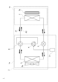
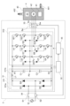
- Block diagram of a refrigeration cycle device is a schematic diagram of a compressor and a control device of a refrigeration cycle device according to an embodiment; 1 is a waveform diagram of a voltage of a smoothing circuit of a drive circuit of a control device according to an embodiment of the present invention; 1 is a part of a flowchart of the operation of a control device according to an embodiment. 1 is a part of a flowchart of the operation of a control device according to an embodiment. 1 is a part of a flowchart of the operation of a control device according to an embodiment. 1 is a part of a flowchart of the operation of a control device according to an embodiment. 1 is a part of a flowchart of the operation of a control device according to an embodiment.
- FIG. 1 is a part of a flowchart of the operation of a control device according to an embodiment. 1 is a part of a flowchart of the operation of a control device according to an embodiment.
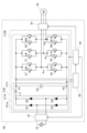
- FIG. 13 is a schematic diagram of a compressor and a control device of a refrigeration cycle device according to a third modification.
- prefixes such as “first” and “second” are added to the names of the components.
- the prefixes such as “first” and “second” may be omitted in consideration of readability of the text.
- 1.1 Configuration 1 is a block diagram of a refrigeration cycle apparatus 1 according to the present embodiment.
- the refrigeration cycle apparatus 1 constitutes, for example, an air conditioner capable of cooling operation and heating operation.
- the refrigeration cycle apparatus 1 includes a refrigeration cycle circuit 2 and a control device 3.
- the refrigeration cycle circuit 2 constitutes a flow path through which the working medium circulates.
- the working medium contains an ethylene-based fluoroolefin as a refrigerant component.
- the ethylene-based fluoroolefin may be an ethylene-based fluoroolefin that undergoes a disproportionation reaction.
- Examples of the ethylene-based fluoroolefin that undergoes a disproportionation reaction include 1,1,2-trifluoroethylene (HFO1123), trans-1,2-difluoroethylene (HFO1132(E)), cis-1,2-difluoroethylene (HFO-1132(Z)), 1,1-difluoroethylene (HFO-1132a), tetrafluoroethylene (CF 2 ⁇ CF 2 , FO1114), and monofluoroethylene (HFO-1141).
- the working medium may contain multiple types of refrigerant components.
- the working medium may contain an ethylene-based fluoroolefin as a main refrigerant component and a compound other than an ethylene-based fluoroolefin as a secondary refrigerant component.
- secondary refrigerant components include hydrofluorocarbons (HFCs), hydrofluoroolefins (HFOs), saturated hydrocarbons, carbon dioxide, etc.
- hydrofluorocarbons examples include difluoromethane, difluoroethane, trifluoroethane, tetrafluoroethane, pentafluoroethane, pentafluorobutane, heptafluorocyclopentane, etc.
- hydrofluoroolefins examples include monofluoropropene, trifluoropropene, tetrafluoropropene, pentafluoropropene, hexafluorobutene, etc.
- saturated hydrocarbons examples include ethane, n-propane, cyclopropane, n-butane, cyclobutane, isobutane (2-methylpropane), methylcyclopropane, n-pentane, isopentane (2-methylbutane), neopentane (2,2-dimethylpropane), methylcyclobutane, etc.
- the working fluid may further contain a disproportionation inhibitor that suppresses the disproportionation reaction of the ethylene-based fluoroolefin.
- the disproportionation inhibitor include saturated hydrocarbons or haloalkanes.
- saturated hydrocarbons include ethane, n-propane, cyclopropane, n-butane, cyclobutane, isobutane (2-methylpropane), methylcyclopropane, n-pentane, isopentane (2-methylbutane), neopentane (2,2-dimethylpropane), methylcyclobutane, and the like.
- n-propane is preferred.
- haloalkanes examples include haloalkanes having 1 or 2 carbon atoms.
- haloalkanes having one carbon atom examples include ( mono )iodomethane ( CH3I ), diiodomethane (CH2I2), dibromomethane ( CH2Br2 ), bromomethane (CH3Br), dichloromethane ( CH2Cl2 ) , chloroiodomethane ( CH2ClI ), dibromochloromethane (CHBr2Cl), tetraiodomethane ( CI4 ), carbon tetrabromide ( CBr4 ), bromotrichloromethane ( CBrCl3 ) , dibromodichloromethane (CBr2Cl2), tribromofluoromethane ( CBr3F ), fluorodiiodomethane (CHFI2) , di
- haloalkanes having 2 carbon atoms examples include 1,1,1-trifluoro-2-iodoethane (CF 3 CH 2 I), monoiodoethane (CH 3 CH 2 I), monobromoethane (CH 3 CH 2 Br ), 1,1,1-triiodoethane (CH 3 CI 3 ), etc.
- the working fluid may contain one or more types of haloalkanes having 1 or 2 carbon atoms. In other words, only one type of haloalkane having 1 or 2 carbon atoms may be used, or two or more types may be used in appropriate combination.
- a pressure sensor (GC61 manufactured by Nagano Keiki Co., Ltd.) was attached to a sealed pressure vessel (stainless steel sealed vessel, internal volume 50 mL) to measure the internal pressure in the pressure vessel, a thermocouple (PL thermocouple ground PL-18-K-A 4-T manufactured by Conax Technologies) to measure the internal temperature in the pressure vessel, and a discharge device to generate a discharge in the pressure vessel.
- a gas cylinder of 1,1,2-trifluoroethylene was connected so that the pressure could be adjusted.
- a mantle heater was installed to heat the entire pressure vessel, and a ribbon heater (flexible ribbon heater 1 m, 200 W manufactured by Tokyo Institute of Technology Co., Ltd.) was installed to heat the piping as well. This constructed an experimental system for the disproportionation reaction.
- Table 1 shows whether or not a disproportionation reaction occurs when the working fluid is 1,1,2-trifluoroethylene alone, a mixed gas adjusted to have a 1,1,2-trifluoroethylene content of 80 mass% and an n-propane content of 20 mass%, a mixed gas adjusted to have a 1,1,2-trifluoroethylene content of 91.5 mass%, an n-propane content of 7.5 mass%, and a difluoroiodomethane content of 1.0 mass%, and a mixed gas adjusted to have a 1,1,2-trifluoroethylene content of 69.5 mass%, a difluoromethane content of 22 mass%, an n-propane content of 7.5 mass%, and a difluoroiodomethane content of 1.0 mass%.
- the pressure was adjusted to 2 MPa in Examples 1 and 2, and 6 MPa in Examples 3 to 5.
- the peak current in Table 1 is the maximum value of the current that flowed during discharge.
- the number of discharges is the number of times discharged at regular intervals under the conditions in question, and if a disproportionation reaction was observed after that number of discharges, the disproportionation reaction was recorded as "Yes,” and if no disproportionation reaction was observed, it was recorded as "No.”
- Example 1 As can be seen from Table 1, no disproportionation reaction was observed in Example 1. Therefore, even if continuous discharge with a peak current of about 80 A was performed multiple times, no disproportionation reaction occurred. As shown in Example 2, when the peak current was large, a disproportionation reaction was observed after two continuous discharges. Therefore, the presence or absence of a disproportionation reaction depends on the magnitude of the peak current. To suppress the disproportionation reaction, it is preferable to keep the peak current below 135 A.
- Example 3 no disproportionation reaction was observed in the working medium of a mixed gas containing n-propane as a disproportionation inhibitor. Therefore, it was confirmed that even in a working medium containing n-propane as a disproportionation inhibitor, the possibility of a disproportionation reaction occurring is extremely low, even if a peak current of about 100 A is continuously discharged multiple times. This shows that in order to suppress disproportionation reactions in a working medium of a mixed gas containing a disproportionation inhibitor, it is preferable to keep the peak current below 135 A.
- Example 4 As can be seen from Table 1, in Example 4, no disproportionation reaction was observed in the working medium of a mixed gas containing n-propane and difluoroiodomethane as disproportionation inhibitors. Therefore, it was confirmed that even in a working medium containing n-propane and difluoroiodomethane as disproportionation inhibitors, the possibility of a disproportionation reaction occurring is extremely low, even if a peak current of about 100 A is continuously discharged multiple times. This shows that in order to suppress disproportionation reactions in a working medium of a mixed gas containing two or more disproportionation inhibitors, it is preferable to keep the peak current below 135 A.
- Example 5 no disproportionation reaction was observed in the working fluid of a mixed gas containing difluoromethane as a disproportionation inhibitor different from n-propane and difluoroiodomethane as a secondary refrigerant component. Therefore, it was confirmed that even in a working fluid containing two or more disproportionation inhibitors and a secondary refrigerant component that does not cause disproportionation, the possibility of a disproportionation reaction occurring is extremely low even if discharge with a peak current of about 100 A is performed multiple times in succession. This shows that in order to suppress disproportionation reactions in a working fluid of a mixed gas containing two or more disproportionation inhibitors and one or more types of secondary refrigerants, it is preferable to keep the peak current below 135 A.
- the refrigeration cycle circuit 2 includes a compressor 4, a first heat exchanger 5, an expansion valve 6, a second heat exchanger 7, and a four-way valve 8.
- the refrigeration cycle device 1 includes an outdoor unit 1a and an indoor unit 1b.
- the outdoor unit 1a includes a control device 3, a compressor 4, a first heat exchanger 5, an expansion valve 6, and a four-way valve 8.
- the outdoor unit 1a further includes a first blower 5a for promoting heat exchange in the first heat exchanger 5.
- the indoor unit 1b includes a second heat exchanger 7.
- the indoor unit 1b further includes a second blower 7a for promoting heat exchange in the second heat exchanger 7.
- the compressor 4 compresses the working medium to increase the pressure of the working medium.
- the compressor 4 will be described in detail later.
- the first heat exchanger 5 and the second heat exchanger 7 exchange heat between the working medium circulating through the refrigeration cycle circuit 2 and external air (e.g., outside air or room air).
- the expansion valve 6 adjusts the pressure (evaporation pressure) of the working medium and the flow rate of the working medium.
- the four-way valve 8 switches the direction of the working medium circulating through the refrigeration cycle circuit 2 between a first direction corresponding to cooling operation and a second direction corresponding to heating operation.
- the first direction is the direction in which the working medium circulates through the refrigeration cycle circuit 2, in the order of the compressor 4, the first heat exchanger 5, the expansion valve 6, and the second heat exchanger 7, as shown by the solid arrow A1 in Figure 1.
- the compressor 4 compresses and discharges the gaseous working medium, which is then sent to the first heat exchanger 5 via the four-way valve 8.
- the first heat exchanger 5 exchanges heat between the outside air and the gaseous working medium, causing the gaseous working medium to condense and become liquefied.
- the liquid working medium is decompressed by the expansion valve 6 and sent to the second heat exchanger 7.
- heat exchange occurs between the liquid working medium and the indoor air, causing the gaseous working medium to evaporate and become a gaseous working medium.
- the gaseous working medium returns to the compressor 4 via the four-way valve 8.
- the first heat exchanger 5 functions as a condenser
- the second heat exchanger 7 functions as an evaporator. Therefore, during cooling, the indoor unit 1b blows air cooled by heat exchange in the second heat exchanger 7 into the room.
- the second direction is the direction in which the working medium circulates through the refrigeration cycle circuit 2, in the order of the compressor 4, the second heat exchanger 7, the expansion valve 6, and the first heat exchanger 5, as shown by the dashed arrow A2 in Figure 1.
- the compressor 4 compresses and discharges the gaseous working medium, which is then sent to the second heat exchanger 7 via the four-way valve 8.
- the second heat exchanger 7 exchanges heat between the indoor air and the gaseous working medium, causing the gaseous working medium to condense and become liquefied.
- the liquid working medium is decompressed by the expansion valve 6 and sent to the first heat exchanger 5.
- heat exchange occurs between the liquid working medium and the outside air, causing the gaseous working medium to evaporate and become a gaseous working medium.
- the gaseous working medium returns to the compressor 4 via the four-way valve 8.
- the first heat exchanger 5 functions as an evaporator
- the second heat exchanger 7 functions as a condenser. Therefore, during heating, the indoor unit 1b blows air warmed by heat exchange in the second heat exchanger 7 into the room.
- the control device 3 controls the compressor 4 of the refrigeration cycle circuit 2.
- Figure 2 is a schematic diagram of the compressor 4 and the control device 3.
- the compressor 4 is, for example, a hermetic compressor.
- the compressor 4 may be of a rotary type, a scroll type, or any other known type.
- the compressor 4 includes a hermetic container 40, a compression mechanism 41, and an electric motor 42.
- the sealed container 40 forms a flow path for the working medium 20.
- the sealed container 40 has a suction pipe 401 and a discharge pipe 402.
- the working medium 20 is sucked into the sealed container 40 from the suction pipe 401, compressed by the compression mechanism 41, and then discharged from the discharge pipe 402 to the outside of the sealed container 40.
- the inside of the sealed container 40 is filled with high-temperature, high-pressure working medium 20 and lubricating oil.
- the bottom of the sealed container 40 forms an oil storage section that stores a mixture of the working medium 20 and lubricating oil.
- the compression mechanism 41 is located inside the sealed container 40 and compresses the working medium.
- the compression mechanism 41 may have a conventionally known configuration.
- the compression mechanism 41 has, for example, a cylinder that forms a compression chamber, a rolling piston that is disposed in the compression chamber inside the cylinder, and a crankshaft that is connected to the rolling piston.
- the electric motor 42 is located inside the sealed container 40 and operates the compression mechanism 41.
- the electric motor 42 is, for example, a brushless motor (three-phase brushless motor).
- the electric motor 42 includes, for example, a rotor fixed to the crankshaft of the compression mechanism 41 and a stator provided around the rotor.
- the stator is, for example, configured by concentrating or dispersing a stator winding (magnet wire, etc.) around a stator core (electromagnetic steel plate, etc.) with an insulating material such as insulating paper interposed between the stator winding.
- the stator winding is covered with an insulating material. Examples of insulating materials include polyethylene terephthalate (PET), polyethylene naphthalate (PEN), aramid polymer, polyphenylene sulfide (PPS), polytetrafluoroethylene (PTFE), etc.
- the compressor 4 may be equipped with an accumulator to prevent liquid compression in the compression chamber of the compression mechanism 41.
- the accumulator separates the working medium into a gaseous working medium and a liquid working medium, and guides only the gaseous working medium from the suction pipe 401 into the inside of the sealed container 40.
- the control device 3 includes a drive circuit 31, a state detection circuit 32, a first protection device 33, a second protection device 34, and a control circuit 35.
- the drive circuit 31 drives the electric motor 42 based on the input power from the power source 10.
- the power source 10 is an AC power source
- the input power is AC power.
- the drive circuit 31 includes a converter circuit 311 and an inverter circuit 312.
- the converter circuit 311 outputs DC output power based on the input power from the power source 10. More specifically, the converter circuit 311 outputs DC output power based on the input power from the power source 10 so that the voltage becomes a first voltage. In other words, the converter circuit 311 converts the input power into DC output power so that the voltage of the DC output power becomes the first voltage.
- the first voltage corresponds to the rated voltage of the drive circuit 31.
- the converter circuit 311 includes a rectifier circuit 311a and a smoothing circuit 311b.
- the rectifier circuit 311a is a diode bridge composed of multiple diodes D1 to D4.
- the power source 10 is connected between the input terminals of the rectifier circuit 311a (the connection point of diodes D1, D2, and the connection point of diodes D3, D4), and the smoothing circuit 311b is connected between the output terminals of the rectifier circuit 311a (the connection point of diodes D1, D3, and the connection point of diodes D2, D4).
- the smoothing circuit 311b smoothes and outputs the voltage between the output terminals of the rectifier circuit 311a.
- the smoothing circuit 311b sets the voltage of the DC output power to a first voltage.
- the smoothing circuit 311b includes a series circuit of an inductor L1 and smoothing capacitors C1 and C2.
- the connection point between the inductor L1 and the smoothing capacitor C1 is the first output point P1 that outputs a voltage corresponding to the first voltage.
- the connection point between the diodes D2 and D4 and the smoothing capacitor C2 is the second output point P2 that outputs a voltage lower than the voltage at the first output point P1.
- the first output point P1 and the second output point P2 determine the voltage of the DC output power.
- the voltage between the first and second output points P1 and P2 corresponds to the voltage of the DC output power.
- the connection point between the smoothing capacitor C1 and the smoothing capacitor C2 is the third output point P3 that outputs a voltage between the voltage at the first output point P1 and the voltage at the second output point P2.
- the first output point P1 is an output point on the high voltage side (high voltage point)
- the second output point P2 is an output point on the low voltage side (low voltage point)
- the third output point P3 is an intermediate voltage point.
- the smoothing capacitor C1 and the smoothing capacitor C2 have the same capacitance. Therefore, the voltage between the voltage at the first output point P1 and the voltage at the third output point P3 is equal to the voltage between the voltage at the second output point P2 and the voltage at the third output point P3. If the voltage between the first output point P1 and the second output point P2 (which corresponds to the first voltage) is E, then the voltage between the first output point P1 and the third output point P3 is E/2, and similarly, the voltage between the second output point P2 and the third output point P3 is E/2. This allows the drive circuit 31 to provide five voltage levels: E, E/2, 0, -E/2, and -E.
- the inverter circuit 312 outputs AC output power to the motor 42 based on the DC output power from the converter circuit 311.
- the AC output power is three-phase AC power.
- the inverter circuit 312 includes a plurality of semiconductor switching elements U1 to U4, V1 to V4, and W1 to W4.
- the semiconductor switching elements U1 to U4, V1 to V4, and W1 to W4 each form a series circuit and are connected between the first output point P1 and the second output point P2.
- connection point of the semiconductor switching elements U1 and U2, the connection point of the semiconductor switching elements V1 and V2, and the connection point of the semiconductor switching elements W1 and W2 are connected to the third output point P3 via diodes D5, D7, and D9, respectively.
- the anodes of diodes D5, D7, and D9 are connected to the third output point P3, and the cathodes of diodes D5, D7, and D9 are connected to the connection point of semiconductor switching elements U1 and U2, the connection point of semiconductor switching elements V1 and V2, and the connection point of semiconductor switching elements W1 and W2, respectively.
- connection point of the semiconductor switching elements U2, U3 constitutes the U-phase output terminal Pu, which is connected to the U-phase input terminal of the motor 42.
- the connection point of the semiconductor switching elements V2, V3 constitutes the V-phase output terminal Pv, which is connected to the V-phase input terminal of the motor 42.
- the connection point of the semiconductor switching elements W2, W3 constitutes the W-phase output terminal Pw, which is connected to the W-phase input terminal of the motor 42.
- connection point of the semiconductor switching elements U3 and U4, the connection point of the semiconductor switching elements V3 and V4, and the connection point of the semiconductor switching elements W3 and W4 are connected to the third output point P3 via diodes D6, D8, and D10, respectively.
- the cathodes of diodes D6, D8, and D10 are connected to the third output point P3, and the anodes of diodes D6, D8, and D10 are connected to the connection point of semiconductor switching elements U3 and U4, the connection point of semiconductor switching elements V3 and V4, and the connection point of semiconductor switching elements W3 and W4, respectively.
- the maximum allowable current of the multiple semiconductor switching elements U1 to U4, V1 to V4, W1 to W4 is set based on the instantaneous abnormal current caused by an abnormality (arc discharge, layer short, etc.) in the drive circuit 31 or the compressor 4, for example, the instantaneous discharge current.
- the inventors have found through testing, etc. that the current value of the instantaneous abnormal current of about ⁇ s to sub-ms is often 135 A. Therefore, the multiple semiconductor switching elements U1 to U4, V1 to V4, W1 to W4 are configured to include one or more protective semiconductor switching elements with a maximum allowable current of less than 135 A.
- the protective semiconductor switching element when an instantaneous abnormal current occurs, the protective semiconductor switching element is destroyed by the abnormal current, and the current is cut off in the protective semiconductor switching element.
- the maximum allowable current of the protective semiconductor switching element may be 130 A or less, 120 A or less, 110 A or less, or 100 A or less. The smaller the maximum allowable current, the shorter the time until the protective semiconductor switching element is damaged by an abnormal current, and it is expected that the possibility of the protective semiconductor switching element being damaged by an abnormal current will increase. However, it is desirable to set the maximum allowable current of the protective semiconductor switching element so that it will not be damaged under normal circumstances.
- the maximum allowable current of the semiconductor switching elements U1, U4, V1, V4, W1, and W4 is less than 135 A, and the maximum allowable current of the semiconductor switching elements U2, U3, V2, V3, W2, and W3 is 135 A or more.
- the semiconductor switching elements U1, U4, V1, V4, W1, and W4 function as protective semiconductor switching elements.
- the semiconductor switching elements U1, U2, V1, V2, W1, and W2 constitute a first semiconductor switching element group connected between the first output point P1 and the motor 42.
- the semiconductor switching elements U3, U4, V3, V4, W3, and W4 constitute a second semiconductor switching element group connected between the second output point P2 and the motor 42.
- the semiconductor switching elements U1 and U2 constitute a U-phase first semiconductor switching element group that is connected between the first output point P1 and the U-phase input terminal of the motor 42.
- the U-phase first semiconductor switching element group constitutes a series circuit of the semiconductor switching elements U1 and U2, and includes the semiconductor switching element U1, which is a protective semiconductor switching element.
- the semiconductor switching element U1 is the semiconductor switching element on the first output point P1 side.
- the semiconductor switching elements U3 and U4 constitute a U-phase second semiconductor switching element group connected between the second output point P2 and the U-phase input terminal of the motor 42.
- the U-phase second semiconductor switching element group constitutes a series circuit of the semiconductor switching elements U3 and U4, and includes the semiconductor switching element U4 which is a protective semiconductor switching element.
- the semiconductor switching element U4 is the semiconductor switching element on the second output point P2 side.
- Table 2 below shows the relationship between the on/off states of the semiconductor switching elements U1 to U4 and the U-phase output voltage Vu at the U-phase output terminal Pu.
- Table 2 shows the relationship between the on/off states of the semiconductor switching elements U1 to U4 and the U-phase output voltage Vu at the U-phase output terminal Pu.
- Table 2 shows the relationship between the on/off states of the semiconductor switching elements U1 to U4 and the U-phase output voltage Vu at the U-phase output terminal Pu.
- Table 2 shows the relationship between the on/off states of the semiconductor switching elements U1 to U4 and the U-phase output voltage Vu at the U-phase output terminal Pu.
- Table 2 shows the relationship between the on/off states of the semiconductor switching elements U1 to U4 and the U-phase output voltage Vu at the U-phase output terminal Pu.
- the semiconductor switching elements V1 and V2 constitute a V-phase first semiconductor switching element group that is connected between the first output point P1 and the V-phase input terminal of the motor 42.
- the V-phase first semiconductor switching element group constitutes a series circuit of the semiconductor switching elements V1 and V2, and includes the semiconductor switching element V1, which is a protective semiconductor switching element.
- the semiconductor switching element V1 is the semiconductor switching element on the first output point P1 side.
- Semiconductor switching elements V3 and V4 constitute a V-phase second semiconductor switching element group connected between the second output point P2 and the V-phase input terminal of the motor 42.
- the V-phase second semiconductor switching element group constitutes a series circuit of semiconductor switching elements V3 and V4, and includes semiconductor switching element V4, which is a protective semiconductor switching element.
- semiconductor switching element V4 is the semiconductor switching element on the second output point P2 side.
- Table 3 shows the relationship between the on/off state of the semiconductor switching elements V1 to V4 and the V-phase output voltage Vv at the V-phase output terminal Pv.
- Table 3 shows the relationship between the on/off state of the semiconductor switching elements V1 to V4 and the V-phase output voltage Vv at the V-phase output terminal Pv.
- Table 3 shows the relationship between the on/off state of the semiconductor switching elements V1 to V4 and the V-phase output voltage Vv at the V-phase output terminal Pv.
- Table 3 shows the relationship between the on/off state of the semiconductor switching elements V1 to V4 and the V-phase output voltage Vv at the V-phase output terminal Pv.
- the semiconductor switching elements W1 and W2 constitute a W-phase first semiconductor switching element group connected between the first output point P1 and the W-phase input terminal of the motor 42.
- the W-phase first semiconductor switching element group constitutes a series circuit of the semiconductor switching elements W1 and W2, and includes the semiconductor switching element W1 which is a protective semiconductor switching element.
- the semiconductor switching element W1 is the semiconductor switching element on the first output point P1 side.
- the semiconductor switching elements W3 and W4 constitute a W-phase second semiconductor switching element group connected between the second output point P2 and the W-phase input terminal of the motor 42.
- the W-phase second semiconductor switching element group constitutes a series circuit of the semiconductor switching elements W3 and W4, and includes the semiconductor switching element W4 which is a protective semiconductor switching element.
- the semiconductor switching element W4 is the semiconductor switching element on the second output point P2 side.
- Table 4 shows the relationship between the on/off state of the semiconductor switching elements W1 to W4 and the W-phase output voltage Vw at the W-phase output terminal Pw.
- Table 3 for the semiconductor switching elements W1 to W4, "1" indicates on and "0" indicates off.
- the W-phase output voltage Vw is expressed by assuming that the potential difference between the first output point P1 and the second output point P2 is E and the voltage at the third output point P3 is 0.
- the semiconductor switching elements U2, U3, V2, V3, W2, and W3 constitute a third semiconductor switching element group connected between the third output point P3 and the motor 42.
- the semiconductor switching elements U2 and U3 constitute a U-phase third semiconductor switching element group connected between the third output point P3 and the U-phase input terminal of the motor 42.
- the semiconductor switching elements V2 and V3 constitute a V-phase third semiconductor switching element group connected between the third output point P3 and the V-phase input terminal of the motor 42.
- the semiconductor switching elements W2 and W3 constitute a W-phase third semiconductor switching element group connected between the third output point P3 and the W-phase input terminal of the motor 42.
- the converter circuit 311 has a plurality of output points including the first to third output points P1 to P3.
- the inverter circuit 312 has a plurality of semiconductor switching element groups including a first semiconductor switching element group (semiconductor switching elements U1, U2, V1, V2, W1, W2) connected between the first output point P1 and the motor 42, a second semiconductor switching element group (semiconductor switching elements U3, U4, V3, V4, W3, W4) connected between the second output point P2 and the motor 42, and a third semiconductor switching element group (semiconductor switching elements U2, U3, V2, V3, W2, W3) connected between the third output point P3 and the motor 42.
- the drive circuit 31 is a so-called multilevel inverter, in particular a three-level inverter.
- the multiple semiconductor switching elements U1-U4, V1-V4, W1-W4 include a first semiconductor switching element group connected between the first output point P1 and the motor 42, and a second semiconductor switching element group connected between the second output point P2 and the motor 42, for each phase of the AC output power.
- Each of the first semiconductor switching element group and the second semiconductor switching element group includes one or more protective semiconductor switching elements.
- the protective semiconductor switching element in any phase of the AC output power, the protective semiconductor switching element is destroyed by an abnormal current, and the current is cut off in the protective semiconductor switching element. Therefore, it is possible to reduce the possibility of an abnormal phenomenon occurring due to an abnormal current, and to improve the suppression of the disproportionation reaction of the working medium 20.
- the semiconductor switching elements U1 to U4, V1 to V4, and W1 to W4 are, for example, transistors.
- transistors include IGBTs (insulated gate bipolar transistors), MOSFETs (metal oxide semiconductor field effect transistors), and bipolar transistors.
- IGBTs include Si-IGBTs and SiC-IGBTs.
- MOSFETs include Si-MOSFETs and SiC-MOSFETs.
- the semiconductor switching elements U1 to U4, V1 to V4, and W1 to W4 are all IGBTs.
- the state detection circuit 32 detects the state of the drive circuit 31.
- the state of the drive circuit 31 is the voltage of the DC output power of the converter circuit 311.
- the state detection circuit 32 is a voltage detector that detects the DC output power of the converter circuit 311 and outputs a detection voltage indicating the voltage of the DC output power.
- the state detection circuit 32 includes a voltage divider circuit connected between the output terminals of the smoothing circuit 311b of the converter circuit 311, that is, between the first output point P1 and the second output point P2, and outputs a detection voltage based on the voltage obtained from the voltage divider circuit.
- the state detection circuit 32 may also output a detection voltage based on the output of the voltage divider circuit and the differential amplifier.
- the non-inverting input terminal and the inverting input terminal of the differential amplifier are connected to both ends of the resistor of the voltage divider circuit, respectively, and the differential amplifier can output the voltage across the resistor as a detection voltage.
- the position where the state detection circuit 32 is connected to the drive circuit 31 is not particularly limited, and may be any position where the DC output power of the converter circuit 311 can be detected.
- the position where the DC output power of the converter circuit 311 can be detected is not limited to within the converter circuit 311, but may be a position within the inverter circuit 312 that is equivalent in circuit terms to the first output point P1 and the second output point P2.
- the voltage divider circuit can have a conventionally known configuration, so a detailed description will be omitted.
- the first protection device 33 is provided to stop the output of AC output power.
- the first protection device 33 includes switches Su, Sv, and Sw interposed between the drive circuit 31 and the motor 42.
- the switches Su, Sv, and Sw are connected between the U-phase, V-phase, and W-phase input terminals of the motor 42 and the U-phase output terminals Pu, Pv, and Pw, respectively.
- the switches Su, Sv, and Sw may be controllable switches such as semiconductor switches and electromagnetic relays.
- the first protection device 33 When the switches Su, Sv, and Sw are closed in the on state, the first protection device 33 enables the output of AC output power from the drive circuit 31 to the motor 42, and when the switches Su, Sv, and Sw are open in the off state, the first protection device 33 stops the output of AC output power from the drive circuit 31 to the motor 42.
- the second protection device 34 is provided to stop the input of input power.
- the second protection device 34 includes switches S1 and S2 interposed between the drive circuit 31 and the power source 10.
- the switches S1 and S2 are respectively connected between the input terminal of the rectifier circuit 311a and the power source 10.
- the switches S1 and S2 may be, for example, a controllable switch such as a semiconductor switch or an electromagnetic relay.
- the control circuit 35 may be realized by, for example, a computer system including at least one processor (microprocessor) and one or more memories.
- the computer system may include one or more A/D converters.
- the one or more A/D converters are used to convert the detection voltage from the state detection circuit 32 from analog to digital format.
- the control circuit 35 controls the drive circuit 31, the first protection device 33, and the second protection device 34.
- the control circuit 35 executes PWM control of a group of multiple semiconductor switching elements of the inverter circuit 312 of the drive circuit 31 so that the drive circuit 31 operates the electric motor 42.
- control circuit 35 controls the switching of the multiple semiconductor switching elements U1 to U4, V1 to V4, and W1 to W4 of the inverter circuit 312 of the drive circuit 31 so that the inverter circuit 312 supplies AC output power (three-phase AC power) to the electric motor 42 based on the DC output power from the smoothing circuit 311b.
- the semiconductor switching elements U1 to U4 have a first state in which the semiconductor switching elements U1 and U2 are on and the semiconductor switching elements U3 and U4 are off, a second state in which the semiconductor switching elements U3 and U4 are on and the semiconductor switching elements U1 and U2 are off, and a third state in which the semiconductor switching elements U2 and U3 are on and the semiconductor switching elements U1 and U4 are off.
- the voltage at the U-phase output terminal Pu is E/2 in the first state, -E/2 in the second state, and 0 in the third state.
- the semiconductor switching elements V1 to V4 There are three states for the semiconductor switching elements V1 to V4: a first state in which the semiconductor switching elements V1 and V2 are on and the semiconductor switching elements V3 and V4 are off; a second state in which the semiconductor switching elements V3 and V4 are on and the semiconductor switching elements V1 and V2 are off; and a third state in which the semiconductor switching elements V2 and V3 are on and the semiconductor switching elements V1 and V4 are off.
- the voltage at the V-phase output terminal Pv is E/2 in the first state, -E/2 in the second state, and 0 in the third state.
- the semiconductor switching elements W1 to W4 have a first state in which the semiconductor switching elements W1 and W2 are on and the semiconductor switching elements W3 and W4 are off, a second state in which the semiconductor switching elements W3 and W4 are on and the semiconductor switching elements W1 and W2 are off, and a third state in which the semiconductor switching elements W2 and W3 are on and the semiconductor switching elements W1 and W4 are off.
- the voltage at the W-phase output terminal Pw is E/2 in the first state, -E/2 in the second state, and 0 in the third state.
- the drive circuit 31 can provide five voltage levels: E, E/2, 0, -E/2, and -E.
- the control circuit 35 controls the switching of the semiconductor switching elements U1-U4, V1-V4, W1-W4 of the inverter circuit 312 of the drive circuit 31 based on, for example, U-phase, V-phase, and W-phase output voltage command values corresponding to the sine wave AC voltages of the U-phase, V-phase, and W-phase of the three-phase AC, respectively, and the first and second carrier triangular waves.
- the value of the first carrier triangular wave is 0 or more, and the value of the second carrier triangular wave is 0 or less.
- the drive circuit 31 can provide five levels of voltage: E, E/2, 0, -E/2, and -E, so that the voltage between the U-phase input terminal and the V-phase input terminal of the motor 42, the voltage between the V-phase input terminal and the W-phase input terminal of the motor 42, and the voltage between the W-phase input terminal and the U-phase input terminal of the motor 42 can each be made closer to a sine wave.
- the control circuit 35 further executes processing to suppress the disproportionation reaction of the working medium 20 circulating through the refrigeration cycle circuit 2 based on the detected voltage from the state detection circuit 32.
- the causes of the disproportionation reaction of the working medium 20 are thought to be heat and radicals. For example, when radicals are generated under high temperature and pressure, the disproportionation reaction of the working medium 20 is thought to proceed. Radicals may be generated, for example, by a discharge phenomenon that may occur when some abnormality occurs in the compressor 4 or the drive circuit 31.
- FIG. 3 is a waveform diagram of the voltage of the DC output power of the converter circuit 311.
- the voltage of the DC output current gradually decreases at times t11 to t12, t21 to t22, t31 to 32, t41 to t42, and t51 to 52, but this voltage decrease is due to the switching of the semiconductor switching elements U1 to U4, V1 to V4, and W1 to W4 of the inverter circuit 312.
- the switching frequency of the inverter circuit 312 is, for example, 1.0 kHz to 5.0 kHz
- the time between time t11 and time t21 is about 0.2 to 1.0 ms.
- a sudden drop in the voltage of the DC output current is observed, which is thought to be due to the occurrence of a discharge phenomenon.
- control circuit 35 determines whether a discharge phenomenon has occurred based on the detected voltage from the state detection circuit 32, and if it determines that a discharge phenomenon has occurred, it stops or limits the operation of the drive circuit 31 to suppress the disproportionation reaction of the working medium circulating through the refrigeration cycle circuit 2.
- the control device 3 detects the signs of a disproportionation reaction based on the changes occurring in the DC output power (voltage of the smoothing circuit 311b) inside the drive circuit 31, not on the changes occurring in the current actually flowing from the drive circuit 31 to the motor 42.
- the time scale of the discharge phenomenon is shorter than the time scale of smoothing (rectification) in the drive circuit 31.
- the time scale of the discharge phenomenon is on the order of ⁇ s. Therefore, it is possible to determine whether a discharge phenomenon is occurring based on the DC output power inside the drive circuit 31.
- the measurement of the DC output power (voltage of the smoothing circuit 311b) inside the drive circuit 31 can be performed in a shorter time and at a shorter cycle than the measurement of the current actually flowing from the drive circuit 31 to the motor 42. This enables the earlier detection of the signs of a disproportionation reaction of the working medium 20. If the signs of a disproportionation reaction of the working medium 20 can be detected earlier in this way, the disproportionation reaction can be suppressed earlier, thereby improving the suppression of the disproportionation reaction.
- the control circuit 35 stops or limits the operation of the drive circuit 31 when the detected voltage falls below a second voltage that is equal to or lower than the first voltage.
- the second voltage is set to determine whether a discharge phenomenon has occurred, which may occur when some abnormality occurs in the compressor 4 or the drive circuit 31. Referring to FIG. 3, if the normal voltage (first voltage) of the DC output current is E, it has been observed that the voltage of the DC output current becomes 0.8E or less, or even 0.3E or less, due to a discharge phenomenon. From this point of view, it is preferable that the second voltage is 0.3 times or more and 0.8 times or less than the first voltage. In this embodiment, the second voltage is 0.8 times the first voltage.
- the operation of the drive circuit 31 can be stopped by either stopping the output of AC output power, stopping the output of DC output power, or stopping the input of input power.
- the operation of the drive circuit 31 can be restricted by lowering the set value of the amplitude of the AC output power, or lowering the set value of the frequency of the AC output power.
- control circuit 35 sets the first protection device 33 to the OFF state to electrically isolate the electric motor 42 from the drive circuit 31 and stop the output of AC output power.
- the control circuit 35 sets the first protection device 33 to the ON state to connect the electric motor 42 to the drive circuit 31.
- the control circuit 35 controls the drive circuit 31 to lower the set value of the amplitude of the AC output power.
- the drive circuit 31 can provide five levels of voltage: E, E/2, 0, -E/2, and -E, so the set value of the amplitude of the AC output power is changed from E to E/2.
- the rotation speed of the motor 42 is lower than when the set value of the amplitude of the AC output power is E.
- control circuit 35 sets the second protection device 34 to the OFF state to electrically isolate the power source 10 from the drive circuit 31 and stop the output of AC output power.
- the control circuit 35 sets the second protection device 34 to the ON state to connect the power source 10 to the drive circuit 31.
- the control circuit 35 stops or limits the operation of the drive circuit 31 in different ways depending on the number of times the detected voltage falls below the second voltage.
- the control circuit 35 executes processing that suppresses the disproportionation reaction to a higher degree as the number of times the detected voltage falls below the second voltage increases. This enables the control device 3 to suppress the disproportionation reaction even when relatively minor discharge phenomena occur consecutively within a short period of time. For example, it is possible to prevent disproportionation reactions from being induced beyond a predetermined energy due to consecutive occurrences of low-energy abnormal states (discharges), thereby improving the safety of using the working medium 20.
- the control circuit 35 stops or limits the operation of the drive circuit 31 in different ways depending on the time difference between the first time when the detected voltage first becomes less than the second voltage and the second time when the detected voltage next becomes less than the second voltage.
- the control circuit 35 executes processing that suppresses the disproportionation reaction to a higher degree the shorter the time difference. This enables the control device 3 to suppress the disproportionation reaction even when relatively minor discharge phenomena occur consecutively within a short period of time. This prevents, for example, a disproportionation reaction from being induced beyond a predetermined energy due to consecutive occurrences of low-energy abnormal states (discharges), improving the safety of using the working medium 20.
- the process for suppressing the disproportionation reaction includes, for example, the first process to the third process.
- the first process is a process for stopping the output of AC output power and resuming the output of AC output power after a standby time has elapsed.
- the second process is a process for stopping the output of AC output power and operating with a lower set value of the amplitude of the AC output power after a standby time has elapsed.
- the third process is a process for stopping the output of AC output power and stopping the input of input power.
- the degree of suppression of the disproportionation reaction increases in the order of the third process, the second process, and the first process. In the first or second process, the longer the standby time, the higher the degree of suppression of the disproportionation reaction.
- the control circuit 35 outputs AC output power to the motor 42 based on the input power of the power source 10 via the drive circuit 31 to drive the compressor 4.
- the control circuit 35 sets the number of abnormalities to 0 (S10).
- the number of abnormalities indicates the number of times the detected voltage is less than the second voltage.
- the number of abnormalities is an indicator of the likelihood of a disproportionation reaction occurring.
- the control circuit 35 acquires the detection voltage from the state detection circuit 32 (S11). The control circuit 35 determines whether the detection voltage is less than the second voltage (S12).
- the control circuit 35 determines whether the detected voltage is less than the second voltage at a predetermined period. It is preferable that the predetermined period here is shorter than the period corresponding to the reference frequency of the inverter circuit 312 (e.g., 1000 to 5000 Hz).
- step S12 if the detected voltage is less than the second voltage (S12: YES), the control circuit 35 adds 1 to the number of abnormalities (S13) and determines whether the number of abnormalities is 1 or less (S14).
- step S14 If the number of abnormalities is 1 or less in step S14 (S14: YES), the control circuit 35 sets the first protection device 33 to the OFF state to stop the output of AC output power (S15). The control circuit 35 determines whether a first standby time has elapsed since the output of AC output power was stopped (S16). The first standby time is, for example, 1 s. When the first standby time has elapsed (S16: YES), the control circuit 35 sets the first protection device 33 to the ON state to resume the output of AC output power (S17), thereby resuming operation of the compressor 4 (S18). Then, the process returns to step S11.
- control circuit 35 stops outputting the AC output power when the detected voltage becomes less than the second voltage, and resumes outputting the AC output power when the first standby time has elapsed since the output of the AC output power was stopped.
- step S14 if the number of abnormalities is not 1 or less (S14: NO), referring to FIG. 5, the control circuit 35 determines whether the time difference between the first time when the detected voltage first becomes less than the second voltage and the second time when the detected voltage next becomes less than the second voltage is within a first predetermined time (step S19).
- the shortness of the time difference is an indicator of the likelihood of a disproportionation reaction occurring.
- the first predetermined time is, for example, about 100 times the period corresponding to the reference frequency of the inverter circuit 312, and is about 20 to 100 ms.
- step S19 if the time difference is within the first predetermined time (step S19: YES), the control circuit 35 sets the first protection device 33 to the OFF state to stop the output of AC output power (S20). The control circuit 35 sets the second protection device 34 to the OFF state to stop the input of input power (S21). The control circuit 35 outputs a first abnormality notification (S22).
- the first abnormality notification indicates that an abnormality has occurred in the refrigeration cycle device 1 that is highly likely to cause a disproportionation reaction.
- the first abnormality notification is output to, for example, the control circuit of the indoor unit 1b and a remote controller. After this, the control circuit 35 stops the operation of the compressor 4 (S23).
- the control circuit 35 stops the output of the AC output power (S20) and stops the input of the input power (S21).
- step S19 the control circuit 35 determines whether the time difference is within a second predetermined time that is longer than the first predetermined time (step S24).
- the second predetermined time is, for example, about 1000 times the period corresponding to the reference frequency of the inverter circuit 312, and is about 200 ms to 1 s.
- step S24 if the time difference is within the second predetermined time (step S24: YES), the control circuit 35 sets the first protection device 33 to the off state to stop the output of the AC output power (S25).
- the control circuit 35 changes the switching control of the semiconductor switching element of the drive circuit 31 so that the set value of the amplitude of the AC output power decreases from E to E/2 (S26).
- the control circuit 35 outputs a second abnormality notification (S27).
- the second abnormality notification indicates that an abnormality that is likely to cause a disproportionation reaction has occurred in the refrigeration cycle device 1.
- the second abnormality notification is output to, for example, the control circuit and remote controller of the indoor unit 1b.
- the control circuit 35 determines whether a fourth waiting time has elapsed since the output of the AC output power was stopped (S28).
- the fourth waiting time is longer than the first waiting time.
- the fourth waiting time is, for example, 60 seconds.
- the control circuit 35 sets the first protection device 33 to an ON state to resume the output of the AC output power (S29), thereby resuming the operation of the compressor 4 (S30). In this case, the set value of the amplitude of the AC output power remains lowered from E to E/2.
- the control circuit 35 stops the output of the AC output power (S25) and reduces the set value of the amplitude of the AC output power (S26). If a fourth standby time, which is longer than the first standby time, has elapsed since the output of the AC output power was stopped, the control circuit 35 resumes the output of the AC output power while keeping the set value of the amplitude of the AC output power reduced (S29).
- control circuit 35 acquires the detection voltage from the state detection circuit 32 (S31). The control circuit 35 determines whether the detection voltage is less than the second voltage (S32).
- step S32 If the detected voltage is less than the second voltage in step S32 (S32: YES), proceed to step S20 in FIG. 5.
- step S32 if the detected voltage is not less than the second voltage (S32: NO), the control circuit 35 determines whether the second monitoring time has elapsed since the compressor 4 restarted operating (S33).
- step S33 if the second monitoring time has elapsed since the compressor 4 restarted operating (S33: YES), the control circuit 35 cancels the reduction in the set value of the amplitude of the AC output power, returns the set value of the amplitude of the AC output power to E (S34), and proceeds to step S11 in FIG. 4.
- step S33 if the second monitoring time has not elapsed since the compressor 4 restarted operation (S33: NO), the process returns to step S31.
- steps S31 to S33 if the detected voltage falls below the second voltage between the time when compressor 4 restarts operation and the time when the second monitoring time has elapsed, the process proceeds to step S20 in FIG. 5, and if the detected voltage does not fall below the second voltage between the time when compressor 4 restarts operation and the time when the second monitoring time has elapsed, the process proceeds to step S34.
- the control circuit 35 cancels the reduction in the set value of the amplitude of the AC output power (S34). If the detected voltage becomes less than the second voltage before the second monitoring time has elapsed after the output of the AC output power is resumed after the fourth waiting time has elapsed (S29) (YES in S32), the control circuit 35 stops the output of the AC output power (S20) and stops the input of the input power (S21).
- step S35 the control circuit 35 determines whether the time difference is within a third predetermined time that is longer than the second predetermined time (step S35).
- the third predetermined time is, for example, about 10,000 times the period corresponding to the reference frequency of the inverter circuit 312, and is about 2 s to 10 s.
- step S35 if the time difference is not within the third predetermined time (step S35: NO), the process returns to step S10, and the control circuit 35 sets the number of abnormalities to 0 (see FIG. 4). In other words, if a sufficient amount of time has passed since the detection of the abnormality, the possibility of a discharge phenomenon occurring is considered to be low, so the number of abnormalities is reset to 0.
- step S35 if the time difference is within the third predetermined time (step S35: YES), the control circuit 35 determines whether the number of abnormalities is 2 or less (S36).
- step S36 if the number of abnormalities is 2 or less (S36: YES), the control circuit 35 sets the first protection device 33 to the OFF state to stop the output of the AC output power (S37).
- the control circuit 35 outputs a third abnormality notification (S38).
- the third abnormality notification indicates that an abnormality that may cause a disproportionation reaction has occurred in the refrigeration cycle device 1.
- the third abnormality notification is output to, for example, the control circuit of the indoor unit 1b and a remote controller.
- the control circuit 35 determines whether a second standby time has elapsed since the output of the AC output power was stopped (S39).
- the second standby time is longer than the first standby time.
- the second standby time is, for example, 10 s.
- the control circuit 35 sets the first protection device 33 to the ON state to resume the output of the AC output power (S40), thereby resuming the operation of the compressor 4 (S41). After that, the process returns to step S11.
- the control circuit 35 stops the output of the AC output power if the detected voltage becomes less than the second voltage before a predetermined time (third predetermined time) has elapsed since the output of the AC output power was resumed after the first standby time had elapsed (S17).
- the control circuit 35 resumes the output of the AC output power when a second standby time longer than the first standby time has elapsed since the output of the AC output power was stopped (S40).
- step S36 if the number of abnormalities is not 2 or less (S36: NO), that is, if the number of abnormalities is 3 or more, the control circuit 35 sets the first protection device 33 to the off state to stop the output of AC output power (S42).
- the control circuit 35 changes the switching control of the semiconductor switching element of the drive circuit 31 so that the set value of the amplitude of the AC output power is reduced from E to E/2 (S43).
- the control circuit 35 outputs a second abnormality notification (S44).
- the control circuit 35 determines whether the third standby time has elapsed since the output of the AC output power was stopped (S45).
- the third standby time is longer than the second standby time.
- the third standby time is, for example, 60 seconds.
- the control circuit 35 sets the first protection device 33 to the ON state to resume the output of the AC output power (S46), thereby resuming the operation of the compressor 4 (S47). In this case, the set value of the amplitude of the AC output power remains lowered from E to E/2.
- the control circuit 35 stops the output of the AC output power (S42) and lowers the set value of the amplitude of the AC output power (S43). If a third standby time, which is longer than the second standby time, has elapsed since the output of the AC output power was stopped, the control circuit 35 resumes the output of the AC output power while keeping the set value of the amplitude of the AC output power lowered (S47).
- control circuit 35 acquires the detection voltage from the state detection circuit 32 (S48). The control circuit 35 determines whether the detection voltage is less than the second voltage (S49).
- step S49 If the detected voltage is less than the second voltage in step S49 (S49: YES), proceed to step S20 in FIG. 5.
- step S49 if the detected voltage is not less than the second voltage (S49: NO), the control circuit 35 determines whether the first monitoring time has elapsed since the compressor 4 restarted operating (S50).
- the first monitoring time may be the same as or different from the second monitoring time in step S33.
- step S50 if the first monitoring time has elapsed since the compressor 4 restarted operating (S50: YES), the control circuit 35 cancels the reduction in the set value of the amplitude of the AC output power, returns the set value of the amplitude of the AC output power to E (S51), and proceeds to step S11 in FIG. 4.
- step S50 if the first monitoring time has not elapsed since the compressor 4 restarted operation (S50: NO), the process returns to step S48.
- steps S48 to S50 if the detected voltage becomes less than the second voltage between the time when compressor 4 restarts operation and the time when the first monitoring time has elapsed, the process proceeds to step S20 in FIG. 5, and if the detected voltage does not become less than the second voltage between the time when compressor 4 restarts operation and the time when the first monitoring time has elapsed, the process proceeds to step S51.
- the control circuit 35 cancels the reduction in the set value of the amplitude of the AC output power (S51). If the detected voltage becomes less than the second voltage before the first monitoring time has elapsed after the output of the AC output power is resumed after the third waiting time has elapsed (S47) (YES in S49), the control circuit 35 stops the output of the AC output power (S20) and stops the input of the input power (S21).
- the multiple semiconductor switching elements U1 to U4, V1 to V4, W1 to W4 of the inverter circuit 312 include protective semiconductor switching elements (semiconductor switching elements U1, U4, V1, V4, W1, W4) whose maximum allowable current is less than 135 A. Therefore, when an instantaneous abnormal current occurs, the protective semiconductor switching elements are destroyed by the abnormal current, and the current is cut off in the protective semiconductor switching elements. This limits or stops the output of AC output power from the drive circuit 31 to the motor 42. Furthermore, when an abnormal current occurs, the control circuit 35 stops or limits the operation of the drive circuit 31, and limits or stops the output of AC output power.
- the protective semiconductor switching elements are destroyed before the control circuit 35 stops or limits the operation of the drive circuit 31. Therefore, the time from the occurrence of an abnormal current to the limiting or stopping of the output of AC output power can be shortened, and the suppression of the disproportionation reaction of the working medium 20 can be improved. In particular, by destroying the protective semiconductor switching element, it becomes possible to suppress the disproportionation reaction of the working medium 20 with zero delay. Furthermore, since the control circuit 35 stops or limits the operation of the drive circuit 31, the continuous input of energy from the drive circuit 31 to the electric motor 42 during an abnormality is suppressed, improving safety. Furthermore, even if the protective semiconductor switching element is not destroyed, the control circuit 35 makes it possible to suppress the disproportionation reaction of the working medium 20.
- the inverter circuit 312 described above is included in the drive circuit 31 that drives the compressor 4 of the refrigeration cycle circuit 2 in which the working medium 20 circulates.
- the inverter circuit 312 includes a plurality of semiconductor switching elements U1 to U4, V1 to V4, and W1 to W4, and outputs AC output power to the compressor 4 based on DC output power.
- the plurality of semiconductor switching elements U1 to U4, V1 to V4, and W1 to W4 include one or more protective semiconductor switching elements (semiconductor switching elements U1, U4, V1, V4, W1, and W4) whose maximum allowable current is less than 135 A. This configuration can shorten the time from the occurrence of an abnormal current to the limiting or stopping of the output of AC output power, and enables improved suppression of the disproportionation reaction.
- the multiple semiconductor switching elements U1-U4, V1-V4, W1-W4 include a first semiconductor switching element group connected between the first output point P1 and the compressor 4, and a second semiconductor switching element group connected between the second output point P2 and the compressor 4, for each phase of the AC output power.
- the first semiconductor switching element group includes at least one of one or more protective semiconductor switching elements
- each of the second semiconductor switching element groups includes at least another one of one or more protective semiconductor switching elements. This configuration can shorten the time from the occurrence of an abnormal current to the limiting or stopping of the output of the AC output power, and enables improved suppression of the disproportionation reaction.
- the first group of semiconductor switching elements and the second group of semiconductor switching elements each constitute a series circuit of semiconductor switching elements. This configuration can shorten the time from the occurrence of an abnormal current to the limiting or stopping of the output of AC output power, and enables improved suppression of the disproportionation reaction.
- one or more protective semiconductor switching elements are IGBTs. This configuration can shorten the time from the occurrence of an abnormal current to the limiting or stopping of the output of AC output power, and enables improved suppression of the disproportionation reaction.
- one or more protective semiconductor switching elements may be MOSFETs. This configuration can shorten the time from the occurrence of an abnormal current to the limiting or stopping of the output of AC output power, and enables improved suppression of the disproportionation reaction.
- one or more protective semiconductor switching elements may be bipolar transistors. This configuration can shorten the time from the occurrence of an abnormal current to the limiting or stopping of the output of AC output power, and enables improved suppression of the disproportionation reaction.
- the drive circuit 31 described above includes an inverter circuit 312 and a converter circuit 311 that outputs DC output power to the inverter circuit 312 based on the input power from the power source 10. This configuration can shorten the time from the occurrence of an abnormal current to the limiting or stopping of the output of AC output power, and enables improved suppression of the disproportionation reaction.
- the control device 3 described above includes a drive circuit 31 and a control circuit 35 that controls the drive circuit 31.
- the control circuit 35 stops or limits the operation of the drive circuit 31 in response to detection of an abnormality in at least one of the compressor 4 and the drive circuit 31. This configuration prevents energy from being continuously input from the drive circuit 31 to the compressor 4 in the event of an abnormality, thereby improving safety. Furthermore, even if the protective semiconductor switching element is not destroyed, it is possible to suppress the disproportionation reaction of the working medium 20.
- the control device 3 further includes a state detection circuit 32 that detects the state of at least one of the compressor 4 and the drive circuit 31.
- the converter circuit 311 outputs DC output power so that the voltage of the DC output power becomes a first voltage.
- the state detection circuit 32 detects the DC output power and outputs a detection voltage indicating the voltage of the DC output power.
- the control circuit 35 stops or limits the operation of the drive circuit 31 when the detection voltage becomes less than a second voltage that is equal to or less than the first voltage. This configuration enables earlier detection of signs of a disproportionation reaction in the working medium 20 and allows for improved suppression of the disproportionation reaction.
- the second voltage is 0.3 to 0.8 times the first voltage. This configuration enables early detection of signs of a disproportionation reaction in the working medium 20 and improves suppression of the disproportionation reaction.
- the refrigeration cycle device 1 described above includes a control device 3 and a refrigeration cycle circuit 2. This configuration enables improved suppression of disproportionation reactions.
- the working medium contains an ethylene-based fluoroolefin. This configuration allows for improved suppression of the disproportionation reaction of the working medium 20.
- the ethylene-based fluoroolefin is 1,1,2-trifluoroethylene, trans-1,2-difluoroethylene, cis-1,2-difluoroethylene, 1,1-difluoroethylene, tetrafluoroethylene, or monofluoroethylene. This configuration enables improved suppression of the disproportionation reaction of the working medium 20.
- the working medium 20 further contains difluoromethane. This configuration enables improved suppression of the disproportionation reaction of the working medium 20.
- the working medium 20 further contains saturated hydrocarbons. This configuration enables improved suppression of the disproportionation reaction of the working medium 20.
- the working medium 20 contains a haloalkane having one or two carbon atoms as a disproportionation inhibitor that suppresses the disproportionation reaction of ethylene-based fluoroolefins. This configuration enables improved suppression of the disproportionation reaction of the working medium 20.
- the saturated hydrocarbons include n-propane. This configuration allows for improved suppression of the disproportionation reaction of the working medium 20.
- the control device 3 described above executes the following control method.
- the control method is executed by the control device 3 that controls the compressor 4 of the refrigeration cycle circuit 2 through which the working medium 20 circulates.
- the drive circuit 31 includes a converter circuit 311 that outputs DC output power based on input power from the power source 10, and an inverter circuit 312 that includes multiple semiconductor switching elements U1 to U4, V1 to V4, W1 to W4 and outputs AC output power to the compressor 4 based on the DC output power.
- the multiple semiconductor switching elements U1 to U4, V1 to V4, W1 to W4 include one or more protective semiconductor switching elements U1, U4, V1, V4, W1, W4 with a maximum allowable current of less than 135 A.
- the control method stops or limits the operation of the drive circuit 31 in response to detection of an abnormality in at least one of the compressor 4 and the drive circuit 31.
- This configuration can shorten the time from the occurrence of an abnormal current to the limiting or stopping of the output of AC output power, and improves the suppression of the disproportionation reaction of the working medium 20. Furthermore, this configuration prevents the drive circuit 31 from continuously supplying energy to the compressor 4 during an abnormality, improving safety. Even if the protective semiconductor switching element is not destroyed, it is possible to suppress the disproportionation reaction of the working medium 20.
- the control method executed by the control device 3 can be realized by a computer system executing a program. This program is executed by a computer system included in the control device 3 that controls the compressor 4 of the refrigeration cycle circuit 2 through which the working medium 20 circulates.
- the drive circuit 31 includes a converter circuit 311 that outputs DC output power based on input power from the power source 10, and an inverter circuit 312 that includes multiple semiconductor switching elements U1 to U4, V1 to V4, W1 to W4 and outputs AC output power to the compressor 4 based on the DC output power.
- the multiple semiconductor switching elements U1 to U4, V1 to V4, W1 to W4 include one or more protective semiconductor switching elements U1, U4, V1, V4, W1, W4 with a maximum allowable current of less than 135 A.
- the program causes the computer system to stop or limit the operation of the drive circuit 31 in response to detection of an abnormality in at least one of the compressor 4 and the drive circuit 31.
- This configuration can shorten the time from the occurrence of an abnormal current to the limiting or stopping of the output of AC output power, and can improve the suppression of the disproportionation reaction of the working medium 20. Furthermore, this configuration prevents the drive circuit 31 from continuously supplying energy to the compressor 4 during an abnormality, improving safety. Even if the protective semiconductor switching element is not destroyed, the control circuit 35 can suppress the disproportionation reaction of the working medium 20.
- Fig. 10 is a schematic diagram of the compressor 4 and the control device 3A of the refrigeration cycle apparatus according to the modified example 1.
- Fig. 10 for the sake of simplicity, only the electric motor 42 is shown in the compressor 4, and the first protection device 33 and the second protection device 34 are simplified.
- the control device 3A includes a drive circuit 31A, a state detection circuit 32, a first protection device 33, a second protection device 34, and a control circuit 35.
- the drive circuit 31A includes a converter circuit 311A and an inverter circuit 312A.
- the converter circuit 311A includes a rectifier circuit 311a and a smoothing circuit 311c.
- the smoothing circuit 311c smoothes and outputs the voltage between the output terminals of the rectifier circuit 311a.
- the smoothing circuit 311c sets the voltage of the DC output power to a first voltage.
- the smoothing circuit 311c includes a series circuit of an inductor L1 and a smoothing capacitor C3.
- the connection point between the inductor L1 and the smoothing capacitor C1 is a first output point P1 that outputs a voltage corresponding to the first voltage.
- the connection point between the diodes D2, D4 and the smoothing capacitor C3 is a second output point P2 that outputs a voltage lower than the voltage at the first output point P1.
- the first output point P1 and the second output point P2 determine the voltage of the DC output power.
- the inverter circuit 312A outputs AC output power to the motor 42 based on the DC output power from the converter circuit 311A.
- the AC output power is three-phase AC power.
- the inverter circuit 312A includes multiple semiconductor switching elements U5, U6, V5, V6, W5, and W6.
- the semiconductor switching elements U5, U6, V5, V6, and W5, W6 each form a series circuit and are connected between the first output point P1 and the second output point P2.
- connection point of the semiconductor switching elements U5, U6 constitutes the U-phase output terminal Pu, which is connected to the U-phase input terminal of the motor 42.
- the connection point of the semiconductor switching elements V5, V6 constitutes the V-phase output terminal Pv, which is connected to the V-phase input terminal of the motor 42.
- the connection point of the semiconductor switching elements W5, W6 constitutes the W-phase output terminal Pw, which is connected to the W-phase input terminal of the motor 42.
- the maximum allowable current of the semiconductor switching elements U5, U6, V5, V6, W5, and W6 is less than 135 A, and all of the semiconductor switching elements U5, U6, V5, V6, W5, and W6 function as protective semiconductor switching elements.
- the semiconductor switching elements U5, V5, and W5 constitute a first semiconductor switching element group connected between the first output point P1 and the motor 42.
- the semiconductor switching elements U5, V5, and W5 constitute a U-, V-, and W-phase first semiconductor switching element group connected between the first output point P1 and the U-, V-, and W-phase input terminals of the motor 42.
- the first semiconductor switching element group may be composed of a single semiconductor switching element.
- the semiconductor switching elements U6, V6, and W6 constitute a second semiconductor switching element group connected between the second output point P2 and the motor 42.
- the semiconductor switching elements U6, V6, and W6 constitute a U-, V-, and W-phase second semiconductor switching element group connected between the second output point P2 and the U-, V-, and W-phase input terminals of the motor 42.
- the second semiconductor switching element group may be composed of a single semiconductor switching element.
- the multiple semiconductor switching elements U5, U6, V5, V6, W5, and W6 of the inverter circuit 312B include protective semiconductor switching elements (semiconductor switching elements U5, U6, V5, V6, W5, and W6) whose maximum allowable current is less than 135 A. Therefore, when an instantaneous abnormal current occurs, the protective semiconductor switching elements are destroyed by the abnormal current, and the current is cut off in the protective semiconductor switching elements. This limits or stops the output of AC output power from the drive circuit 31A to the motor 42. Furthermore, when an abnormal current occurs, the control circuit 35 stops or limits the operation of the drive circuit 31A, and limits or stops the output of AC output power.
- the protective semiconductor switching elements are destroyed before the control circuit 35 stops or limits the operation of the drive circuit 31A. Therefore, the time from the occurrence of an abnormal current to the limiting or stopping of the output of AC output power can be shortened, and the suppression of the disproportionation reaction of the working medium 20 can be improved. In particular, by destroying the protective semiconductor switching element, it becomes possible to suppress the disproportionation reaction of the working medium 20 with zero delay. Furthermore, because the control circuit 35 stops or limits the operation of the drive circuit 31A, the continuous input of energy from the drive circuit 31A to the motor 42 during an abnormality is suppressed, improving safety. Furthermore, even if the protective semiconductor switching element is not destroyed, the control circuit 35 makes it possible to suppress the disproportionation reaction of the working medium 20.
- the inverter circuit 312A described above is included in the drive circuit 31A that drives the compressor 4 of the refrigeration cycle circuit 2 in which the working medium 20 circulates.
- the inverter circuit 312A includes multiple semiconductor switching elements U5, U6, V5, V6, W5, and W6, and outputs AC output power to the compressor 4 based on the DC output power.
- the multiple semiconductor switching elements U5, U6, V5, V6, W5, and W6 include one or more protective semiconductor switching elements (semiconductor switching elements U5, U6, V5, V6, W5, and W6) with a maximum allowable current of less than 135 A. This configuration can shorten the time from the occurrence of an abnormal current to the limiting or stopping of the output of AC output power, and enables improved suppression of the disproportionation reaction.
- the multiple semiconductor switching elements U5, U6, V5, V6, W5, and W6 include a first semiconductor switching element group connected between the first output point P1 and the motor 42 and a second semiconductor switching element group connected between the second output point P2 and the motor 42 for each phase of the AC output power.
- the first semiconductor switching element group includes at least one of one or more protective semiconductor switching elements (semiconductor switching elements U5, V5, and W5)
- each of the second semiconductor switching element groups includes at least another one of one or more protective semiconductor switching elements (semiconductor switching elements U6, V6, and W6).
- the protective semiconductor switching element in any phase of the AC output power, the protective semiconductor switching element is destroyed by an abnormal current, and the current is cut off in the protective semiconductor switching element. Therefore, the possibility of an abnormal phenomenon occurring due to an abnormal current can be reduced, and the suppression of the disproportionation reaction of the working medium 20 can be improved.
- FIG. 11 is a schematic diagram of a compressor 4 and a control device 3B of a refrigeration cycle apparatus according to Modification 2.
- Fig. 11 for the sake of simplicity, only the electric motor 42 is shown in the compressor 4, and the first protection device 33 and the second protection device 34 are simplified.
- the control device 3B includes a drive circuit 31B, a state detection circuit 32, a first protection device 33, a second protection device 34, and a control circuit 35.
- the drive circuit 31B includes a converter circuit 311A and an inverter circuit 312B.
- the inverter circuit 312B outputs AC output power to the motor 42 based on the DC output power from the converter circuit 311A.
- the AC output power is three-phase AC power.
- the inverter circuit 312B includes multiple semiconductor switching elements U7 to U10, V7 to V10, and W7 to W10.
- Each of the semiconductor switching elements U7, U8 and U9, U10 constitutes a parallel circuit.
- the parallel circuit of the semiconductor switching elements U7, U8 and the parallel circuit of the semiconductor switching elements U9, U10 constitute a series circuit and are connected between the first output point P1 and the second output point P2.
- the semiconductor switching elements U7, U8 are turned on or off simultaneously, and the parallel circuit of the semiconductor switching elements U7, U8 is used as one semiconductor switching element.
- the semiconductor switching elements U9, U10 are turned on or off simultaneously, and the parallel circuit of the semiconductor switching elements U9, U10 is used as one semiconductor switching element.
- Each of the semiconductor switching elements V7, V8 and V9, V10 constitutes a parallel circuit.
- the parallel circuit of the semiconductor switching elements V7, V8 and the parallel circuit of the semiconductor switching elements V9, V10 constitute a series circuit and are connected between the first output point P1 and the second output point P2.
- the semiconductor switching elements V7, V8 are turned on or off simultaneously, and the parallel circuit of the semiconductor switching elements V7, V8 is used as one semiconductor switching element.
- the semiconductor switching elements V9, V10 are turned on or off simultaneously, and the parallel circuit of the semiconductor switching elements V9, V10 is used as one semiconductor switching element.
- Each of the semiconductor switching elements W7, W8 and W9, W10 constitutes a parallel circuit.
- the parallel circuit of the semiconductor switching elements W7, W8 and the parallel circuit of the semiconductor switching elements W9, W10 constitute a series circuit and are connected between the first output point P1 and the second output point P2.
- the semiconductor switching elements W7, W8 are turned on or off simultaneously, and the parallel circuit of the semiconductor switching elements W7, W8 is used as one semiconductor switching element.
- the semiconductor switching elements W9, W10 are turned on or off simultaneously, and the parallel circuit of the semiconductor switching elements W9, W10 is used as one semiconductor switching element.
- connection point between the parallel circuit of semiconductor switching elements U7, U8 and the parallel circuit of semiconductor switching elements U9, U10 constitutes a U-phase output terminal Pu connected to the U-phase input terminal of the motor 42.
- the connection point between the parallel circuit of semiconductor switching elements V7, V8 and the parallel circuit of semiconductor switching elements V9, V10 constitutes a V-phase output terminal Pv connected to the V-phase input terminal of the motor 42.
- the connection point between the parallel circuit of semiconductor switching elements W7, W8 and the parallel circuit of semiconductor switching elements W9, W10 constitutes a W-phase output terminal Pw connected to the W-phase input terminal of the motor 42.
- the maximum allowable current of the semiconductor switching elements U7 to U10, V7 to V10, and W7 to W10 is less than 135 A, and all of the semiconductor switching elements U7 to U10, V7 to V10, and W7 to W10 function as protective semiconductor switching elements.
- the semiconductor switching elements U7, U8, V7, V8, W7, and W8 constitute a first semiconductor switching element group connected between the first output point P1 and the motor 42.
- the semiconductor switching elements U9, U10, V9, V10, W9, and W10 constitute a second semiconductor switching element group connected between the second output point P2 and the motor 42.
- the semiconductor switching elements U7 and U8 constitute a U-phase first semiconductor switching element group that is connected between the first output point P1 and the U-phase input terminal of the motor 42.
- the U-phase first semiconductor switching element group constitutes a parallel circuit of the semiconductor switching elements U7 and U8, and includes the semiconductor switching elements U7 and U8 that are protective semiconductor switching elements.
- the semiconductor switching elements U9 and U10 constitute a U-phase second semiconductor switching element group that is connected between the second output point P2 and the U-phase input terminal of the motor 42.
- the U-phase second semiconductor switching element group constitutes a parallel circuit of the semiconductor switching elements U9 and U10, and includes the semiconductor switching elements U9 and U10 that are protective semiconductor switching elements.
- the semiconductor switching elements V7 and V8 constitute a V-phase first semiconductor switching element group that is connected between the first output point P1 and the V-phase input terminal of the motor 42.
- the V-phase first semiconductor switching element group constitutes a parallel circuit of the semiconductor switching elements V7 and V8, and includes the semiconductor switching elements V7 and V8 that are protective semiconductor switching elements.
- the semiconductor switching elements V9 and V10 constitute a V-phase second semiconductor switching element group that is connected between the second output point P2 and the V-phase input terminal of the motor 42.
- the V-phase second semiconductor switching element group constitutes a parallel circuit of the semiconductor switching elements V9 and V10, and includes the semiconductor switching elements V9 and V10 that are protective semiconductor switching elements.
- the semiconductor switching elements W7 and W8 constitute a W-phase first semiconductor switching element group that is connected between the first output point P1 and the W-phase input terminal of the motor 42.
- the W-phase first semiconductor switching element group constitutes a parallel circuit of the semiconductor switching elements W7 and W8, and includes the semiconductor switching elements W7 and W8 that are protective semiconductor switching elements.
- the semiconductor switching elements W9 and W10 constitute a W-phase second semiconductor switching element group that is connected between the second output point P2 and the W-phase input terminal of the motor 42.
- the W-phase second semiconductor switching element group constitutes a parallel circuit of the semiconductor switching elements W9 and W10, and includes the semiconductor switching elements W9 and W10 that are protective semiconductor switching elements.
- the parallel circuit of semiconductor switching elements U7, U8 is used as one semiconductor switching element.
- the maximum allowable current of semiconductor switching elements U7, U8 is set so that the maximum allowable current of the parallel circuit of semiconductor switching elements U7, U8 is less than 135 A.
- the maximum allowable current of semiconductor switching elements U7, U8 may be set according to the ratio of the internal resistances of semiconductor switching elements U7, U8. This also applies to the parallel circuit of semiconductor switching elements U9, U10, the parallel circuit of semiconductor switching elements V7, V8, the parallel circuit of semiconductor switching elements V9, V10, the parallel circuit of semiconductor switching elements W7, W8, and the parallel circuit of semiconductor switching elements W9, W10.
- the multiple semiconductor switching elements U7 to U10, V7 to V10, and W7 to W10 of the inverter circuit 312B include protective semiconductor switching elements (semiconductor switching elements U7 to U10, V7 to V10, and W7 to W10) whose maximum allowable current is less than 135 A. Therefore, when an instantaneous abnormal current occurs, the protective semiconductor switching elements are destroyed by the abnormal current, and the current is cut off in the protective semiconductor switching elements. This limits or stops the output of AC output power from the drive circuit 31B to the motor 42. Furthermore, when an abnormal current occurs, the control circuit 35 stops or limits the operation of the drive circuit 31B, and limits or stops the output of AC output power.
- the protective semiconductor switching elements are destroyed before the control circuit 35 stops or limits the operation of the drive circuit 31B. Therefore, the time from the occurrence of an abnormal current to the limiting or stopping of the output of AC output power can be shortened, and the suppression of the disproportionation reaction of the working medium 20 can be improved. In particular, by destroying the protective semiconductor switching element, it becomes possible to suppress the disproportionation reaction of the working medium 20 with zero delay. Furthermore, because the control circuit 35 stops or limits the operation of the drive circuit 31B, the continuous input of energy from the drive circuit 31B to the motor 42 during an abnormality is suppressed, improving safety. Furthermore, even if the protective semiconductor switching element is not destroyed, the control circuit 35 makes it possible to suppress the disproportionation reaction of the working medium 20.
- the inverter circuit 312B described above is included in the drive circuit 31B that drives the compressor 4 of the refrigeration cycle circuit 2 through which the working medium 20 circulates.
- the inverter circuit 312B includes multiple semiconductor switching elements U7-U10, V7-V10, W7-W10, and outputs AC output power to the compressor 4 based on the DC output power.
- the multiple semiconductor switching elements U7-U10, V7-V10, W7-W10 include one or more protective semiconductor switching elements (semiconductor switching elements U7-U10, V7-V10, W7-W10) with a maximum allowable current of less than 135 A. This configuration can shorten the time from the occurrence of an abnormal current to the limiting or stopping of the output of AC output power, and enables improved suppression of the disproportionation reaction.
- the voltage of the DC output power is determined by the first and second output points P1 and P2.
- the multiple semiconductor switching elements U7-U10, V7-V10, and W7-W10 include a first semiconductor switching element group connected between the first output point P1 and the motor 42, and a second semiconductor switching element group connected between the second output point P2 and the motor 42, for each phase of the AC output power.
- the first semiconductor switching element group includes at least one of one or more protective semiconductor switching elements (semiconductor switching elements U7, U8, V7, V8, W7, and W8)
- the second semiconductor switching element group includes at least another one of one or more protective semiconductor switching elements (semiconductor switching elements U9, U10, V9, V10, W9, and W10).
- the protective semiconductor switching element in any phase of the AC output power, the protective semiconductor switching element is destroyed by an abnormal current, and the current is cut off in the protective semiconductor switching element. This reduces the possibility of abnormal phenomena occurring due to abnormal currents, and improves the suppression of the disproportionation reaction of the working medium 20.
- each of the first group of semiconductor switching elements and the second group of semiconductor switching elements constitutes a parallel circuit of semiconductor switching elements.
- the maximum allowable current of the parallel circuit is less than 135 A. This configuration can shorten the time from the occurrence of an abnormal current to the limiting or stopping of the output of AC output power, and enables improved suppression of the disproportionation reaction.
- Fig. 12 is a schematic diagram of a compressor 4 and a control device 3C of a refrigeration cycle device according to Modification 3.
- Fig. 12 for simplicity of illustration, only the electric motor 42 of the compressor 4 is illustrated.
- the control device 3C includes a drive circuit 31, a state detection circuit 32, a first protection device 33, a second protection device 34, a control circuit 35, and a third protection device 36.
- the third protection device 36 is provided to stop the output of DC output power.
- the third protection device 36 includes switches S3, S4, and S5 interposed between the converter circuit 311 and the inverter circuit 312 of the drive circuit 31.
- the switch S3 is commonly connected between the first output point P1 and the semiconductor switching elements U1, V1, and W1.
- the switch S4 is commonly connected between the second output point P2 and the semiconductor switching elements U4, V4, and W4.
- the switch S5 is commonly connected between the third output point P3 and the connection point between diodes D5 and D6, the connection point between diodes D7 and D8, and the connection point between diodes D9 and D10.
- the switches S3, S4, and S5 may be controllable switches such as semiconductor switches or electromagnetic relays.
- the third protection device 36 allows the output of DC output power from the converter circuit 311 to the inverter circuit 312 when the switches S3, S4, and S5 are closed in the on state, and stops the output of DC output power from the converter circuit 311 to the inverter circuit 312 when the switches S3, S4, and S5 are open in the off state.
- the safety level increases in the order of stopping the input of input power, stopping the output of DC output power, and stopping the output of AC output power. Therefore, after the operation of the first protection device 33, the third protection device 36 may be operated before the operation of the second protection device 34. Note that if the third protection device 36 is present, the second protection device 34 may be omitted.
- the semiconductor switching elements U7 to U10, V7 to V10, and W7 to W10 do not have to be used as protective semiconductor switching elements.
- the maximum allowable current of one of the semiconductor switching elements U7 and U8 constituting the parallel circuit may be less than 135 A, and the maximum allowable current of the other may be 135 A or more. Even in this case, the maximum allowable current of the parallel circuit is set to be less than 135 A. Even if one of the semiconductor switching elements U7 and U8 constituting the parallel circuit is damaged, the balance between the phases of the AC output power is lost, and the rotation of the motor 42 is stopped.
- semiconductor switching elements are operated in parallel, it is generally desirable to connect semiconductor switching elements of the same performance in parallel in the parallel circuit of semiconductor switching elements.
- semiconductor switching elements When only one of the semiconductor switching elements constituting a parallel circuit is used as a protective semiconductor switching element, it is desirable to select the semiconductor switching elements so that their characteristics (switching characteristics such as switching speed, internal resistance such as the internal resistance between C and E) are substantially the same and their maximum allowable currents are different.
- the semiconductor switching elements U1 to U4, V1 to V4, and W1 to W4 may all be MOSFETs.
- MOSFETs have lower durability than IGBTs. For example, even if the maximum allowable current is the same, a MOSFET may be destroyed more quickly than an IGBT. Therefore, by using a MOSFET as the protective semiconductor switching element, the time until the protective semiconductor switching element is destroyed may be shorter than when an IGBT is used.
- stopping the operation of the drive circuit 31 may include one or more of stopping the output of AC output power, stopping the output of DC output power, or stopping the input of input power.
- Restricting the operation of the drive circuit 31 may include one or more of reducing the set value of the amplitude of the AC output power, or reducing the set value of the frequency of the AC output power.
- control circuit 35 may gradually stop and decelerate the electric motor 42. As one example, the control circuit 35 may gradually reduce the effective value of the AC output power supplied to the electric motor 42 by gradually reducing at least one of the amplitude and frequency of the AC output power.
- control circuit 35 is not necessarily limited to the operations shown in the flowcharts shown in Figures 4 to 9.
- the flowcharts shown in Figures 4 to 9 are merely examples.
- the processes of steps S19 to S23 i.e., the processes of stopping the output of AC output power and stopping the input of input power
- the processes of steps S24 to S28 i.e., the processes of stopping the output of AC output power and lowering the set value of the amplitude of the AC output power after the standby time has elapsed
- the processes of steps S29 to S34, steps S35 to S41, or steps S42 to S51 are not essential.
- the control circuit 35 does not necessarily have to stop or limit the operation of the drive circuit 31 in a different manner depending on the time difference between the first time when the detected voltage first becomes less than the second voltage and the second time when the detected voltage next becomes less than the second voltage, or the number of times the detected voltage becomes less than the second voltage.
- the first protection device 33 is not limited to a circuit configuration including switches Su, Sv, and Sw, and may include a circuit configuration that adjusts the magnitude of the AC output power output from the drive circuit 31 to the electric motor 42, for example, the magnitude of the voltage.
- the first protection device 33 may be disposed within the drive circuit 31.
- the second protection device 34 is not limited to a circuit configuration including switches S1 and S2, and may include a circuit configuration that adjusts the magnitude of the input power input from the power source 10 to the drive circuit 31, for example, the magnitude of the voltage.
- the second protection device 34 may be disposed within the drive circuit 31.
- the third protection device 36 is not limited to a circuit configuration including switches S3, S4, and S5, but may include a circuit configuration that adjusts the magnitude of the DC output power output from the converter circuit 311 to the inverter circuit 312, for example, the magnitude of the voltage.
- the control device 3 does not necessarily have to include both the first protection device 33 and the second protection device 34, and may include either the first protection device 33 or the second protection device 34, and if the drive circuit 31 has a function of adjusting the AC output power, the first and second protection devices 33, 34 can be omitted.
- the control circuit 35 may stop the output of AC output power to the motor 42 by turning on the semiconductor switching elements V1 to V4 of the inverter circuit 312 and turning off the remaining semiconductor switching elements U1 to U4, W1 to W4.
- the first protection device 33 may be omitted.
- the state detection circuit 32 is not limited to a configuration that detects the voltage value of the DC output power of the converter circuit 311.
- the state detection circuit 32 may be configured to detect the state of at least one of the compressor 4 and the drive circuit 31.
- the state of the drive circuit 31 may be the current value of the current flowing through the drive circuit 31.
- the current value of the current flowing through the drive circuit 31 may include at least one of the current values of the output AC current of the U-phase, V-phase, and W-phase legs of the drive circuit 31.
- the abnormality of the drive circuit 31 is a current abnormality.
- the control circuit 35 may detect the current abnormality in response to the current value of the current flowing through the drive circuit 31 detected by the state detection circuit 32 exceeding a predetermined current value.
- the current value of the current flowing through the drive circuit 31 may include the current value of the DC current flowing between the converter circuit 311 and the inverter circuit 312 of the drive circuit 31.
- control circuit 35 may determine that a current abnormality has occurred in the drive circuit 31 if the current value of the DC current flowing between the converter circuit 311 and the inverter circuit 312 of the drive circuit 31 exceeds a predetermined current value.
- control circuit 35 determines that a current abnormality has occurred in the drive circuit 31 (i.e., when a current abnormality in the drive circuit 31 is detected), it may stop or limit the operation of the drive circuit 31.
- the state of the compressor 4 may include at least one of the phase current of the compressor 4 and the rotation speed of the motor 42 of the compressor 4.
- the current value of the phase current of the compressor 4 may include the current values of the U-phase, V-phase, and W-phase currents.
- the abnormality of the compressor 4 may include an abnormality related to a layer short of the compressor 4.
- An abnormality related to a layer short of the compressor 4 may include the layer short of the compressor 4 itself, an abnormality that may cause a layer short of the compressor 4, and an abnormality that may be caused by a layer short of the compressor 4.
- Specific examples of abnormalities related to a layer short of the compressor 4 include a layer short of the compressor 4, a leakage current of the compressor 4, and an open-phase operation of the compressor 4.
- the control circuit 35 may determine whether an abnormality of the compressor 4 has occurred based on the state of the compressor 4 detected by the state detection circuit 32. For example, if an imbalance in the phase currents of the compressor 4 occurs, the control circuit 35 may determine that an abnormality related to a layer short in the compressor 4 has occurred. Also, if a deviation in the rotation speed of the motor 42 of the compressor 4 occurs, there is a possibility that an abnormality related to a layer short in the compressor 4 has occurred. When the control circuit 35 determines that an abnormality related to a layer short has occurred in the compressor 4 (i.e., when an abnormality related to a layer short in the compressor 4 is detected), it may stop or limit the operation of the drive circuit 31.
- the power source 10 may be any of a variety of AC power sources, particularly a commercial power source.
- the voltage and frequency of the commercial power source vary depending on the country, the drive circuit 31 may be configured to be capable of driving the electric motor 42 using any of a variety of commercial power sources.
- the drive circuit 31 can be configured to supply AC output power corresponding to the type of the electric motor 42, etc.
- the AC output power is not limited to three-phase AC power, and can be single-phase AC power.
- the converter circuit 311 may have a plurality of third output points.
- the plurality of third output points may output different voltages.
- the inverter circuit 312 may have a plurality of third semiconductor switching element groups respectively connected between the plurality of third output points and the motor 42. If the total number of the first output point P1, the second output point P2, and the plurality of third output points P3 is n, the drive circuit 31 can provide a voltage of (2 ⁇ n-1) levels. By increasing n, the voltage waveform applied to the motor 42 by the drive circuit 31 can be made closer to a sine wave.
- the circuit configuration of the inverter circuit 312 is not limited to the circuit configuration in FIG. 2.
- the circuit configuration of the inverter circuit 312 in FIG. 2 is a so-called NPC (Neutral-Point-Clamped) type, but may be an A-NPC (Advanced-NPC) type.
- the inverter circuit 312 only needs to have a plurality of semiconductor switching element groups that are respectively connected between a plurality of output points with different voltages and the electric motor.
- the plurality of semiconductor switching elements that make up the plurality of semiconductor switching element groups may include semiconductor switching elements that are included in common to two or more semiconductor switching element groups.
- the refrigeration cycle device is not limited to an air conditioner (so-called room air conditioner (RAC)) configured with one indoor unit connected to one outdoor unit.
- the refrigeration cycle device may be an air conditioner (so-called package air conditioner (PAC), building multi air conditioner (VRF)) configured with multiple indoor units connected to one or multiple outdoor units.
- the refrigeration cycle device is not limited to an air conditioner, and may be a refrigeration or cooling device such as a refrigerator or freezer.
- the abnormality notifications such as the first to third abnormality notifications may be issued directly or indirectly.
- Direct issuing is when the air conditioner outputs the abnormality notification directly using the outdoor unit 1a, indoor unit 1b, or remote controller, etc.
- the abnormality notification may be output using light from a light source device (LED, red light, warning indicator lamp, etc.) provided on the outdoor unit 1a, indoor unit 1b, or remote controller of the air conditioner, sound from a sound generating device (speaker, buzzer, alarm, sound generator, alarm, etc.), or visual display (message display, backlight flashing, etc.) by a display device (display, display panel, etc.).
- Indirect issuing is when the abnormality notification is output and/or stored outside the air conditioner via a communication network such as the Internet or a server.
- Indirect notifications include push notifications (notifications to mobile phones and smartphones), notifications to voice assistants (Alexa Echo, Google Home, etc.), automatic reporting to the manufacturer or maintenance company, sending a message to the management company's monitoring equipment, notification to a service center, etc., reporting to a fire engine or security company, and saving the information in the abnormality history of a storage device.
- control device 3 may acquire various index values (state values) when diagnosing an abnormality in the refrigeration cycle circuit 2.
- index values used in diagnosing an abnormality in the refrigeration cycle circuit 2 include suction pressure/evaporation saturation temperature, discharge pressure/condensation saturation temperature, suction gas refrigerant temperature, discharge gas refrigerant temperature, condenser outlet refrigerant temperature, evaporator inlet refrigerant temperature, evaporator outlet refrigerant temperature, load side blown air temperature, receiver liquid level, number of discharge precursor detections, number of warnings issued, number of operation restrictions, and number of operation stops.
- the results of the diagnosis by the control device 3 are preferably stored in the internal memory of the control device 3 or an external server or the like for a predetermined period of time (e.g., 1 to 3 years) or more.
- the history of abnormality notifications by the control device 3 is preferably stored in the internal memory of the control device 3 or an external server or the like for a predetermined period of time (e.g., 1 to 3 years) or more.
- An inverter circuit included in a drive circuit that drives a compressor of a refrigeration cycle circuit in which a working medium circulates includes a plurality of semiconductor switching elements, and outputs AC output power to the compressor based on the DC output power;
- the plurality of semiconductor switching elements include one or more protective semiconductor switching elements having a maximum allowable current of less than 135 A. Inverter circuit.
- a voltage of the DC output power is defined at first and second output points;
- the plurality of semiconductor switching elements are arranged to provide, for each phase of AC output power, a first semiconductor switching element group connected between the first output point and the compressor; a second semiconductor switching element group connected between the second output point and the compressor; Including, the first semiconductor switching element group includes at least one of the one or more protection semiconductor switching elements, and the second semiconductor switching element group includes at least another of the one or more protection semiconductor switching elements; 2.
- Each of the first semiconductor switching element group and the second semiconductor switching element group constitutes a series circuit of semiconductor switching elements.
- each of the first semiconductor switching element group and the second semiconductor switching element group constitutes a parallel circuit of semiconductor switching elements;
- the maximum allowable current of the parallel circuit is less than 135 A.
- the one or more protective semiconductor switching elements are IGBTs.
- the inverter circuit according to any one of aspects 1 to 4.
- the one or more protective semiconductor switching elements are MOSFETs.
- the inverter circuit according to any one of aspects 1 to 4.
- the one or more protective semiconductor switching elements are bipolar transistors.
- the inverter circuit according to any one of aspects 1 to 4.
- Aspect 8 An inverter circuit according to any one of aspects 1 to 7; a converter circuit that outputs the DC output power to the inverter circuit based on an input power from a power source; Equipped with Drive circuit.
- a drive circuit according to aspect 8 A control circuit for controlling the drive circuit; Equipped with The control circuit stops or limits the operation of the drive circuit in response to detection of an abnormality in at least one of the compressor and the drive circuit. Control device.
- a state detection circuit for detecting a state of at least one of the compressor and the drive circuit, the converter circuit outputs the DC output power such that a voltage of the DC output power becomes a first voltage; the state detection circuit detects the DC output power and outputs a detection voltage indicative of a voltage of the DC output power; the control circuit stops or limits the operation of the drive circuit when the detected voltage becomes less than a second voltage that is equal to or less than the first voltage.
- the second voltage is 0.3 to 0.8 times the first voltage.
- the compressor includes: A sealed container that forms a flow path of the working medium; a compression mechanism located within the sealed container and configured to compress the working medium; an electric motor located within the sealed container for operating the compression mechanism; Equipped with The inverter circuit outputs the AC output power to the electric motor.
- the control device of any one of aspects 9 to 11.
- a control device according to any one of aspects 9 to 12; The refrigeration cycle circuit; Equipped with Refrigeration cycle equipment.
- the working medium comprises an ethylene-based fluoroolefin;
- the refrigeration cycle apparatus of aspect 13 comprises an ethylene-based fluoroolefin;
- the ethylenic fluoroolefin is 1,1,2-trifluoroethylene, trans-1,2-difluoroethylene, cis-1,2-difluoroethylene, 1,1-difluoroethylene, tetrafluoroethylene, or monofluoroethylene;
- the refrigeration cycle apparatus of aspect 14 is 1,1,2-trifluoroethylene, trans-1,2-difluoroethylene, cis-1,2-difluoroethylene, 1,1-difluoroethylene, tetrafluoroethylene, or monofluoroethylene;
- the working medium further comprises difluoromethane.
- the refrigeration cycle apparatus of aspect 13 The refrigeration cycle apparatus of aspect 13.
- the working medium further comprises a saturated hydrocarbon.
- the refrigeration cycle apparatus of aspect 13 The refrigeration cycle apparatus of aspect 13.
- the working fluid contains a haloalkane having 1 or 2 carbon atoms as a disproportionation inhibitor for suppressing the disproportionation reaction of the ethylenic fluoroolefin.
- the saturated hydrocarbons include n-propane.
- a control method executed by a control device that controls a compressor of a refrigeration cycle circuit in which a working medium circulates comprising:
- the drive circuit includes: A converter circuit that outputs DC output power based on input power from a power supply; an inverter circuit including a plurality of semiconductor switching elements and configured to output an AC output power to the compressor based on the DC output power; Equipped with The plurality of semiconductor switching elements include one or more protective semiconductor switching elements having a maximum allowable current of less than 135 A,
- the control method includes stopping or limiting operation of the drive circuit in response to detection of an abnormality in at least one of the compressor and the drive circuit. Control methods.
- a program executed by a computer system provided in a control device that controls a compressor of a refrigeration cycle circuit in which a working medium circulates The drive circuit includes: A converter circuit that outputs DC output power based on input power from a power supply; an inverter circuit including a plurality of semiconductor switching elements and configured to output an AC output power to the compressor based on the DC output power; Equipped with The plurality of semiconductor switching elements include one or more protective semiconductor switching elements having a maximum allowable current of less than 135 A,
- the program causes the computer system to stop or limit operation of the drive circuit in response to detection of an abnormality in at least one of the compressor and the drive circuit. program.
- Aspects 2 to 7, 10 to 12, and 14 to 19 are optional elements and are not required. Aspects 2 to 7, 10 to 12, and 14 to 19 can be appropriately combined with aspect 20 or 21.
- This disclosure is applicable to inverter circuits, drive circuits, control devices, refrigeration cycle devices, control methods, and programs. Specifically, this disclosure is applicable to an inverter circuit for a refrigeration cycle circuit in which the working medium contains an ethylene-based fluoroolefin as a refrigerant component, a drive circuit including the inverter circuit, a control device including the drive circuit, a refrigeration cycle device including the refrigeration cycle circuit and a control device, a control method executed by the control device, and a program (computer program) used in the control device.
Landscapes
- Engineering & Computer Science (AREA)
- Power Engineering (AREA)
- Physics & Mathematics (AREA)
- Mechanical Engineering (AREA)
- Thermal Sciences (AREA)
- General Engineering & Computer Science (AREA)
- Inverter Devices (AREA)
- Control Of Ac Motors In General (AREA)
Priority Applications (4)
| Application Number | Priority Date | Filing Date | Title |
|---|---|---|---|
| EP24779976.0A EP4693878A1 (en) | 2023-03-31 | 2024-03-22 | Inverter circuit, drive circuit, control device, refrigeration cycle device, control method, and program |
| CN202480023519.3A CN121058152A (zh) | 2023-03-31 | 2024-03-22 | 逆变器电路、驱动电路、控制装置、制冷循环装置、控制方法、程序 |
| JP2025510721A JPWO2024203858A1 (https=) | 2023-03-31 | 2024-03-22 | |
| US19/343,580 US20260025087A1 (en) | 2023-03-31 | 2025-09-29 | Inverter circuit, drive circuit, control device, refrigeration cycle device, control method, and program |
Applications Claiming Priority (2)
| Application Number | Priority Date | Filing Date | Title |
|---|---|---|---|
| JP2023-059379 | 2023-03-31 | ||
| JP2023059379 | 2023-03-31 |
Related Child Applications (1)
| Application Number | Title | Priority Date | Filing Date |
|---|---|---|---|
| US19/343,580 Continuation US20260025087A1 (en) | 2023-03-31 | 2025-09-29 | Inverter circuit, drive circuit, control device, refrigeration cycle device, control method, and program |
Publications (1)
| Publication Number | Publication Date |
|---|---|
| WO2024203858A1 true WO2024203858A1 (ja) | 2024-10-03 |
Family
ID=92906454
Family Applications (1)
| Application Number | Title | Priority Date | Filing Date |
|---|---|---|---|
| PCT/JP2024/011313 Ceased WO2024203858A1 (ja) | 2023-03-31 | 2024-03-22 | インバータ回路、駆動回路、制御装置、冷凍サイクル装置、制御方法、プログラム |
Country Status (5)
| Country | Link |
|---|---|
| US (1) | US20260025087A1 (https=) |
| EP (1) | EP4693878A1 (https=) |
| JP (1) | JPWO2024203858A1 (https=) |
| CN (1) | CN121058152A (https=) |
| WO (1) | WO2024203858A1 (https=) |
Citations (9)
| Publication number | Priority date | Publication date | Assignee | Title |
|---|---|---|---|---|
| JPS54111645A (en) * | 1978-02-20 | 1979-09-01 | Mitsubishi Electric Corp | Surge absorption indicating circuit |
| JP2009106036A (ja) * | 2007-10-22 | 2009-05-14 | Toshiba Carrier Corp | インバータおよび冷凍サイクル装置 |
| JP2012182921A (ja) * | 2011-03-02 | 2012-09-20 | Mitsubishi Electric Corp | インバータ装置および空気調和機 |
| WO2012157765A1 (ja) | 2011-05-19 | 2012-11-22 | 旭硝子株式会社 | 作動媒体および熱サイクルシステム |
| WO2012157764A1 (ja) | 2011-05-19 | 2012-11-22 | 旭硝子株式会社 | 作動媒体および熱サイクルシステム |
| JP2017003197A (ja) * | 2015-06-11 | 2017-01-05 | パナソニックIpマネジメント株式会社 | 冷凍サイクル装置 |
| JP2018061328A (ja) * | 2016-10-04 | 2018-04-12 | ダイキン工業株式会社 | インバータ基板及びその故障検出方法 |
| WO2019172008A1 (ja) | 2018-03-05 | 2019-09-12 | パナソニックIpマネジメント株式会社 | 冷凍サイクル装置 |
| JP2022122870A (ja) * | 2017-04-13 | 2022-08-23 | パナソニックIpマネジメント株式会社 | 冷凍サイクル装置 |
-
2024
- 2024-03-22 EP EP24779976.0A patent/EP4693878A1/en active Pending
- 2024-03-22 JP JP2025510721A patent/JPWO2024203858A1/ja active Pending
- 2024-03-22 CN CN202480023519.3A patent/CN121058152A/zh active Pending
- 2024-03-22 WO PCT/JP2024/011313 patent/WO2024203858A1/ja not_active Ceased
-
2025
- 2025-09-29 US US19/343,580 patent/US20260025087A1/en active Pending
Patent Citations (9)
| Publication number | Priority date | Publication date | Assignee | Title |
|---|---|---|---|---|
| JPS54111645A (en) * | 1978-02-20 | 1979-09-01 | Mitsubishi Electric Corp | Surge absorption indicating circuit |
| JP2009106036A (ja) * | 2007-10-22 | 2009-05-14 | Toshiba Carrier Corp | インバータおよび冷凍サイクル装置 |
| JP2012182921A (ja) * | 2011-03-02 | 2012-09-20 | Mitsubishi Electric Corp | インバータ装置および空気調和機 |
| WO2012157765A1 (ja) | 2011-05-19 | 2012-11-22 | 旭硝子株式会社 | 作動媒体および熱サイクルシステム |
| WO2012157764A1 (ja) | 2011-05-19 | 2012-11-22 | 旭硝子株式会社 | 作動媒体および熱サイクルシステム |
| JP2017003197A (ja) * | 2015-06-11 | 2017-01-05 | パナソニックIpマネジメント株式会社 | 冷凍サイクル装置 |
| JP2018061328A (ja) * | 2016-10-04 | 2018-04-12 | ダイキン工業株式会社 | インバータ基板及びその故障検出方法 |
| JP2022122870A (ja) * | 2017-04-13 | 2022-08-23 | パナソニックIpマネジメント株式会社 | 冷凍サイクル装置 |
| WO2019172008A1 (ja) | 2018-03-05 | 2019-09-12 | パナソニックIpマネジメント株式会社 | 冷凍サイクル装置 |
Non-Patent Citations (1)
| Title |
|---|
| See also references of EP4693878A1 |
Also Published As
| Publication number | Publication date |
|---|---|
| CN121058152A (zh) | 2025-12-02 |
| EP4693878A1 (en) | 2026-02-11 |
| US20260025087A1 (en) | 2026-01-22 |
| JPWO2024203858A1 (https=) | 2024-10-03 |
Similar Documents
| Publication | Publication Date | Title |
|---|---|---|
| WO2019172008A1 (ja) | 冷凍サイクル装置 | |
| CN103477545A (zh) | 电力变换装置、马达驱动装置以及制冷空气调节装置 | |
| JP2013162719A (ja) | 突入電流防止装置 | |
| WO2024203858A1 (ja) | インバータ回路、駆動回路、制御装置、冷凍サイクル装置、制御方法、プログラム | |
| US12372285B2 (en) | Device management system for inverter compressor | |
| JP5780982B2 (ja) | 電力変換装置並びにそれを備えた圧縮機、送風機、空気調和機及び冷蔵庫 | |
| WO2024203857A1 (ja) | 制御装置、放流装置、冷凍サイクル装置、制御方法、プログラム | |
| US11211890B2 (en) | Power conversion apparatus and air-conditioning apparatus | |
| WO2024203908A1 (ja) | コンバータ回路、駆動回路、制御装置、冷凍サイクル装置、制御方法、プログラム | |
| WO2024203926A1 (ja) | 駆動回路、放流装置、制御装置、冷凍サイクル装置、制御方法、プログラム | |
| EP4517224A1 (en) | Refrigeration cycle device | |
| EP4534924A1 (en) | Refrigeration cycle device | |
| US20260110476A1 (en) | Control device, refrigeration cycle device, control method, program | |
| WO2025070609A1 (ja) | 冷凍サイクル回路の運転方法、冷凍サイクル用組成物、冷凍サイクル装置、制御方法、プログラム | |
| WO2025028193A1 (ja) | 制御装置、冷凍サイクル装置 | |
| US20250290502A1 (en) | Refrigeration cycle device | |
| JP6132911B2 (ja) | 逆流防止装置、電力変換装置、モータ駆動装置及び冷凍空気調和装置 | |
| WO2025182075A1 (ja) | 電力変換装置、モータ駆動装置及び空気調和装置 | |
| EP2980973B1 (en) | Backflow prevention device, power conversion device, and cooling air-conditioning device | |
| WO2025084086A1 (ja) | 冷凍サイクル装置、光検知回路、制御装置、制御方法、プログラム | |
| US11611285B2 (en) | Power converter and air conditioner | |
| WO2024176332A1 (ja) | 電力変換装置、モータ駆動装置及び冷凍サイクル適用機器 | |
| WO2025041299A1 (ja) | 空気調和装置および異常検出方法 | |
| WO2025115103A1 (ja) | 空気調和装置 | |
| WO2025074540A1 (ja) | ヒートポンプ装置、空気調和機、ヒートポンプ給湯器、冷蔵庫、および冷凍機 |
Legal Events
| Date | Code | Title | Description |
|---|---|---|---|
| 121 | Ep: the epo has been informed by wipo that ep was designated in this application |
Ref document number: 24779976 Country of ref document: EP Kind code of ref document: A1 |
|
| ENP | Entry into the national phase |
Ref document number: 2025510721 Country of ref document: JP Kind code of ref document: A |
|
| WWE | Wipo information: entry into national phase |
Ref document number: 2025510721 Country of ref document: JP |
|
| WWE | Wipo information: entry into national phase |
Ref document number: 2024779976 Country of ref document: EP |
|
| NENP | Non-entry into the national phase |
Ref country code: DE |
|
| ENP | Entry into the national phase |
Ref document number: 2024779976 Country of ref document: EP Effective date: 20251031 |
|
| ENP | Entry into the national phase |
Ref document number: 2024779976 Country of ref document: EP Effective date: 20251031 |
|
| ENP | Entry into the national phase |
Ref document number: 2024779976 Country of ref document: EP Effective date: 20251031 |
|
| ENP | Entry into the national phase |
Ref document number: 2024779976 Country of ref document: EP Effective date: 20251031 |
|
| ENP | Entry into the national phase |
Ref document number: 2024779976 Country of ref document: EP Effective date: 20251031 |
|
| ENP | Entry into the national phase |
Ref document number: 2024779976 Country of ref document: EP Effective date: 20251031 |
|
| ENP | Entry into the national phase |
Ref document number: 2024779976 Country of ref document: EP Effective date: 20251031 |
|
| ENP | Entry into the national phase |
Ref document number: 2024779976 Country of ref document: EP Effective date: 20251031 |
|
| WWP | Wipo information: published in national office |
Ref document number: 2024779976 Country of ref document: EP |