WO2024203737A1 - 半導体素子搭載用基板 - Google Patents
半導体素子搭載用基板 Download PDFInfo
- Publication number
- WO2024203737A1 WO2024203737A1 PCT/JP2024/011070 JP2024011070W WO2024203737A1 WO 2024203737 A1 WO2024203737 A1 WO 2024203737A1 JP 2024011070 W JP2024011070 W JP 2024011070W WO 2024203737 A1 WO2024203737 A1 WO 2024203737A1
- Authority
- WO
- WIPO (PCT)
- Prior art keywords
- semiconductor element
- element mounting
- substrate
- mounting board
- protective layer
- Prior art date
- Legal status (The legal status is an assumption and is not a legal conclusion. Google has not performed a legal analysis and makes no representation as to the accuracy of the status listed.)
- Ceased
Links
Images


Classifications
-
- H—ELECTRICITY
- H10—SEMICONDUCTOR DEVICES; ELECTRIC SOLID-STATE DEVICES NOT OTHERWISE PROVIDED FOR
- H10W—GENERIC PACKAGES, INTERCONNECTIONS, CONNECTORS OR OTHER CONSTRUCTIONAL DETAILS OF DEVICES COVERED BY CLASS H10
- H10W40/00—Arrangements for thermal protection or thermal control
- H10W40/20—Arrangements for cooling
-
- H—ELECTRICITY
- H05—ELECTRIC TECHNIQUES NOT OTHERWISE PROVIDED FOR
- H05K—PRINTED CIRCUITS; CASINGS OR CONSTRUCTIONAL DETAILS OF ELECTRIC APPARATUS; MANUFACTURE OF ASSEMBLAGES OF ELECTRICAL COMPONENTS
- H05K1/00—Printed circuits
- H05K1/02—Details
-
- H—ELECTRICITY
- H10—SEMICONDUCTOR DEVICES; ELECTRIC SOLID-STATE DEVICES NOT OTHERWISE PROVIDED FOR
- H10H—INORGANIC LIGHT-EMITTING SEMICONDUCTOR DEVICES HAVING POTENTIAL BARRIERS
- H10H20/00—Individual inorganic light-emitting semiconductor devices having potential barriers, e.g. light-emitting diodes [LED]
- H10H20/80—Constructional details
- H10H20/85—Packages
- H10H20/857—Interconnections, e.g. lead-frames, bond wires or solder balls
-
- H—ELECTRICITY
- H10—SEMICONDUCTOR DEVICES; ELECTRIC SOLID-STATE DEVICES NOT OTHERWISE PROVIDED FOR
- H10H—INORGANIC LIGHT-EMITTING SEMICONDUCTOR DEVICES HAVING POTENTIAL BARRIERS
- H10H20/00—Individual inorganic light-emitting semiconductor devices having potential barriers, e.g. light-emitting diodes [LED]
- H10H20/80—Constructional details
- H10H20/85—Packages
- H10H20/858—Means for heat extraction or cooling
- H10H20/8581—Means for heat extraction or cooling characterised by their material
-
- H—ELECTRICITY
- H10—SEMICONDUCTOR DEVICES; ELECTRIC SOLID-STATE DEVICES NOT OTHERWISE PROVIDED FOR
- H10H—INORGANIC LIGHT-EMITTING SEMICONDUCTOR DEVICES HAVING POTENTIAL BARRIERS
- H10H29/00—Integrated devices, or assemblies of multiple devices, comprising at least one light-emitting semiconductor element covered by group H10H20/00
- H10H29/80—Constructional details
- H10H29/85—Packages
- H10H29/8508—Package substrates, e.g. submounts
-
- H—ELECTRICITY
- H10—SEMICONDUCTOR DEVICES; ELECTRIC SOLID-STATE DEVICES NOT OTHERWISE PROVIDED FOR
- H10W—GENERIC PACKAGES, INTERCONNECTIONS, CONNECTORS OR OTHER CONSTRUCTIONAL DETAILS OF DEVICES COVERED BY CLASS H10
- H10W70/00—Package substrates; Interposers; Redistribution layers [RDL]
- H10W70/60—Insulating or insulated package substrates; Interposers; Redistribution layers
- H10W70/67—Insulating or insulated package substrates; Interposers; Redistribution layers characterised by their insulating layers or insulating parts
- H10W70/69—Insulating materials thereof
-
- H—ELECTRICITY
- H10—SEMICONDUCTOR DEVICES; ELECTRIC SOLID-STATE DEVICES NOT OTHERWISE PROVIDED FOR
- H10H—INORGANIC LIGHT-EMITTING SEMICONDUCTOR DEVICES HAVING POTENTIAL BARRIERS
- H10H29/00—Integrated devices, or assemblies of multiple devices, comprising at least one light-emitting semiconductor element covered by group H10H20/00
- H10H29/20—Assemblies of multiple devices comprising at least one light-emitting semiconductor device covered by group H10H20/00
- H10H29/24—Assemblies of multiple devices comprising at least one light-emitting semiconductor device covered by group H10H20/00 comprising multiple light-emitting semiconductor devices
Definitions
- the present invention relates to a substrate for mounting semiconductor elements.
- Patent Document 1 discloses a substrate for mounting semiconductor elements that includes a base material made of metal, an insulating layer, and an intermediate layer disposed between the base material and the insulating layer.
- Patent Document 1 Even with prior art such as Patent Document 1, there was still room for improvement in technology for preventing defects caused by deformation of the substrate in a substrate for mounting semiconductor elements.
- the substrate for mounting semiconductor elements described in Patent Document 1 the substrate is made of a metal that is relatively easily deformed, so there is a risk that the substrate may be deformed due to forces acting on it during handling and various inspections in the manufacturing process. Deformation of the substrate can cause defects such as cracks forming in the insulating layer, so technology for preventing deformation of the substrate has been desired.
- the present invention aims to provide a technology that suppresses defects caused by deformation of the base material in substrates for mounting semiconductor elements.
- the present invention has been made to solve at least some of the problems described above, and can be realized in the following form.
- a substrate for mounting semiconductor elements includes a base material made of metal, an electrode connected to a semiconductor element, and a protective layer disposed between the base material and the electrode, the protective layer being made of a material harder than the metal forming the base material.
- the protective layer disposed between the metal substrate and the electrode is formed from a material harder than the metal that forms the substrate. This makes it possible to suppress deformation of the substrate even if a force that would deform the substrate acts on the semiconductor element mounting board. This makes it possible to suppress the occurrence of defects due to deformation of the substrate.
- the protective layer may be formed of a metal.
- the protective layer is formed of, for example, a metal that is less likely to crack than ceramic. This can further suppress deformation of the substrate, thereby further suppressing the occurrence of defects due to deformation of the substrate.
- the material forming the protective layer may have a higher natural potential in salt water than the metal forming the base material.
- the protective layer may be formed of a material that is corrosion-resistant to sulfur gas. According to this configuration, when the semiconductor element mounting substrate on which the semiconductor element is mounted is actually used, the protective layer can suppress corrosion of the base material caused by sulfur gas present in the usage environment.
- the semiconductor element mounting substrate of the above embodiment may include an insulating layer disposed between the substrate and the electrode, and the protective layer may be disposed between the substrate and the insulating layer.
- the protective layer is formed before the insulating layer is formed in the manufacturing process of the semiconductor element mounting substrate, so that deformation of the substrate can be suppressed before the insulating layer is formed. This makes it possible to suppress, for example, the occurrence of cracks in the insulating layer due to deformation of the substrate.
- the insulating layer may be made of any one of Al2O3 , SiO2 , Y2O3 , AlN, Si3N4 , and SIC .
- the insulating layer is made of any one of Al2O3 , SiO2 , Y2O3 , AlN, Si3N4 , and SIC . This can improve the insulation of the insulating layer.
- an insulating layer may be disposed between the base material and the electrode, and the protective layer may be disposed between the insulating layer and the electrode.
- the protective layer can prevent a force acting on the electrode from acting on the insulating layer. Therefore, damage to the insulating layer can be prevented.
- the insulating layer may be made of any one of Al2O3 , SiO2, Y2O3, AlN, Si3N4, and SIC. According to this configuration, the insulating layer is made of any one of Al2O3 , SiO2 , Y2O3 , AlN , Si3N4 , and SIC . This can improve the insulation of the insulating layer.
- the base material may be formed in a flat plate shape, and the protective layer may be formed on each of a pair of main surfaces of the base material.
- the thickness of the protective layer may be 0.5 ⁇ m or more and 10 ⁇ m or less.
- the protective layer may contain any one of a nickel-cobalt alloy, a nickel-phosphorus alloy, or a nickel-boron alloy.
- any one of the nickel-cobalt alloy, nickel-phosphorus alloy, or nickel-boron alloy contained in the protective layer can be formed by plating. This allows the protective layer to be formed relatively easily in the manufacturing process of the semiconductor device mounting substrate.
- the base material may be formed from a material containing copper or aluminum as a main component.
- the base material is formed from a material containing copper or aluminum as a main component, which has high heat dissipation properties, and therefore the heat dissipation properties of the semiconductor element mounting substrate can be improved.
- the present invention can be realized in various forms, such as a product including a substrate for mounting semiconductor elements, a method for manufacturing a substrate for mounting semiconductor elements, and a method for inspecting a substrate for mounting semiconductor elements.
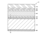
- FIG. 1 is a schematic cross-sectional view of a semiconductor element mounting board according to a first embodiment.
- FIG. 2 is a schematic cross-sectional view of a semiconductor package.
- FIG. 5 is a schematic cross-sectional view of a semiconductor element mounting board according to a second embodiment.
- FIG. 11 is a schematic cross-sectional view of a semiconductor element mounting board according to a third embodiment.
- Fig. 1 is a schematic cross-sectional view of a semiconductor device mounting board 1 according to the first embodiment.
- Fig. 2 is a schematic cross-sectional view of a semiconductor package 5 including the semiconductor device mounting board 1 according to the first embodiment.
- the semiconductor device mounting board 1 according to the present embodiment supports an optical semiconductor such as a light emitting diode (LED) or a semiconductor laser (LD) as a semiconductor device 5a, and functions as a heat dissipation board that dissipates heat generated during light emission to the outside.
- the semiconductor device mounting board 1 includes a base material 10, a protective layer 20, an adhesion layer 30, an insulating layer 40, an adhesion layer 50, a bonding layer 60, and an electrode 70.
- the substrate 10 is a member having a flat plate shape, and serves as the base of the semiconductor element mounting substrate 1. In this embodiment, the thickness of the substrate 10 is 1 mm.
- the substrate 10 is made of a metal. In this embodiment, the substrate 10 is made of copper (Cu).
- the substrate 10 may be made of a material whose main component is copper, aluminum (Al), or a material whose main component is aluminum.
- the term "main component” refers to a component that is greater than 50% by mass in the target material.
- the substrate 10 may be made of an alloy of copper and aluminum.
- the protective layer 20 is disposed between the substrate 10 and the electrode 70, more specifically, between the substrate 10 and the adhesive layer 30.
- the protective layer 20 is provided on one of the pair of main surfaces 11, 12 of the substrate 10.
- the protective layer 20 is formed of a material harder than the metal forming the substrate 10.
- the "material harder than the metal forming the substrate 10" refers to, for example, a material having a Vickers hardness greater than the Vickers hardness of the metal forming the substrate 10.
- the protective layer 20 is formed of a metal that is less likely to break than ceramics and the like.
- the protective layer 20 is formed of a metal containing a nickel-cobalt alloy (Ni-Co).
- the thickness of the protective layer 20 is 0.5 ⁇ m or more and 10 ⁇ m or less.
- the protective layer 20 can transmit the heat generated in the semiconductor element 5a to the substrate 10 while suppressing deformation of the substrate 10.
- the protective layer 20 may be made of a metal containing either a nickel-phosphorus alloy (Ni-P) or a nickel-boron alloy (Ni-B), or it may be made of tungsten (W) or molybdenum (Mo).
- the material forming the protective layer 20 is a material that has a higher natural potential in salt water than the copper forming the base material 10.
- Salt water refers to water with a mass concentration of sodium chloride (NaCl) of 5% or less. This makes it difficult for the protective layer 20 to corrode even when it comes into contact with metal materials that may come into electrical contact with the semiconductor element mounting substrate 1, such as copper, titanium (Ti), nickel, and cobalt, in salt water.
- the protective layer 20 is formed of a material that is more corrosion-resistant to sulfide gas ( H2S ) than the copper that forms the base material 10.
- H2S corrosion-resistant to sulfide gas
- corrosion resistance to sulfide gas refers to a property that corrosion caused by sulfide gas does not progress easily in an environment where the volume concentration of sulfide gas is 15 ppm or less. This allows the protective layer 20 to suppress corrosion of the base material 10 caused by sulfide gas in the environment during actual use.
- the adhesion layer 30 is disposed between the protective layer 20 and the insulating layer 40.
- the adhesion layer 30 is made of titanium and has a thickness of, for example, 0.5 ⁇ m.
- the adhesion layer 30 adheres the protective layer 20 and the insulating layer 40 to each other, and also prevents cracks from forming in the insulating layer 40 due to differences in thermal expansion coefficients.
- the insulating layer 40 is disposed between the substrate 10 and the electrode 70, more specifically, between the adhesion layer 30 and the adhesion layer 50.
- the insulating layer 40 is formed of any one of Al2O3 , SiO2 , Y2O3 , AlN, Si3N4 , and SIC.
- the insulating layer 40 is made of Al2O3 and has a thickness of, for example, 5 ⁇ m .
- the insulating layer 40 insulates the substrate 10, which is made of metal , from the electrode 70.
- the adhesion layer 50 is disposed between the insulating layer 40 and the bonding layer 60.
- the adhesion layer 50 is made of titanium and has a thickness of, for example, 0.2 ⁇ m.
- the adhesion layer 50 adheres the insulating layer 40 and the bonding layer 60 to each other, and also prevents cracks from forming in the insulating layer 40 due to differences in thermal expansion coefficients.
- the bonding layer 60 is disposed between the adhesion layer 50 and the electrode 70.
- the bonding layer 60 is made of palladium (Pd) and has a thickness of, for example, 0.07 ⁇ m.
- the bonding layer 60 improves the bonding strength between the adhesion layer 50 and the electrode 70.
- the electrode 70 is connected to the semiconductor element 5a via the bump 6 (see FIG. 2).
- the electrode 70 is made of gold (Au) and has a thickness of, for example, 3.0 ⁇ m.
- the semiconductor package 5 comprises a semiconductor element mounting substrate 1, a semiconductor element 5a, a phosphor 5b, and a resin portion 5c (see FIG. 2).
- the phosphor 5b is provided on the opposite side of the semiconductor element 5a, which is connected to the semiconductor element mounting substrate 1 by a bump 6, from the semiconductor element 5a, which is connected to the semiconductor element mounting substrate 1.
- the phosphor 5b converts the wavelength of light emitted by the semiconductor element 5a, which is an optical semiconductor, and releases the converted light to the outside.
- the resin portion 5c seals the semiconductor element 5a and the phosphor 5b.
- a method for manufacturing the semiconductor element mounting substrate 1 of this embodiment will be described.
- a nickel-cobalt alloy is deposited on one side of a copper flat plate member that serves as the base material 10, forming a protective layer 20.
- an adhesion layer 30, an insulating layer 40, an adhesion layer 50, a bonding layer 60, and an electrode 70 are deposited in this order on the protective layer 20, and the semiconductor element mounting substrate 1 is manufactured.
- the features of the semiconductor element mounting board 1 of this embodiment will be described while touching upon the problems of a semiconductor element mounting board not provided with a protective layer 20 as a comparative example.
- a load is applied to the electrodes of the semiconductor element mounting board in a probe inspection process, a chip mounting process, etc., and the substrate may be dented in the portion where the load is applied.
- a handling tool comes into contact with the semiconductor element mounting board being handled, and a force from the tool is applied.
- the substrate may be deformed.
- the insulating layer laminated on the substrate is also deformed in the same way, and cracks may be formed in the insulating layer. Cracks in the insulating layer cause dielectric breakdown in the semiconductor element mounting board.
- the semiconductor element mounting substrate 1 of this embodiment has a protective layer 20 between the substrate 10 and the electrode 70, which is formed of a material harder than the metal that forms the substrate 10.
- the protective layer 20 is less likely to deform, and the substrate 10 is less likely to be dented.
- the protective layer 20 is less likely to deform, and the substrate 10 is less likely to deform.
- the insulating layer 40 is also less likely to deform, and therefore insulation breakdown due to deformation of the substrate 10 is less likely to occur in the insulating layer 40.
- the comparative example semiconductor element mounting substrate has a layer made of chromium as an intermediate layer, so electrons tend to move easily at the interface with the metal contained in the comparative example semiconductor element mounting substrate. This may cause galvanic corrosion. In addition, it may react excessively with the etching solution used to etch electrodes, etc., resulting in over-etching.
- the protective layer 20 of the semiconductor element mounting substrate 1 of this embodiment is formed from a nickel-cobalt alloy that has a higher natural potential in salt water than the copper that forms the base material 10. This reduces the potential difference between the base material 10 and the protective layer 20, making it less susceptible to corrosion by salt water and etching by the etching solution used in the manufacturing process.
- the protective layer 20 disposed between the copper substrate 10 and the electrode 70 is formed of a nickel-cobalt alloy, which is a material harder than the copper that forms the substrate 10. This makes it possible to suppress deformation of the substrate 10 even if a force that would deform the substrate 10 acts on the semiconductor element mounting substrate 1 during the manufacturing process of the semiconductor element mounting substrate 1. This makes it possible to suppress the occurrence of defects due to deformation of the substrate 10.
- the protective layer 20 is formed of, for example, a metal that is less likely to crack than ceramic. This can further suppress deformation of the base material 10, thereby further suppressing the occurrence of defects due to deformation of the base material 10.
- the protective layer 20 is formed of a nickel-cobalt alloy that has a higher natural potential in salt water than the copper that forms the base material 10.
- the protective layer 20 can suppress corrosion of the base material 10 caused by exposure to salt water.
- the protective layer 20 is formed of a nickel-cobalt alloy that has corrosion resistance against sulfide gas. As a result, during actual use of the semiconductor element mounting substrate 1 on which the semiconductor element 5a is mounted, the protective layer 20 can suppress corrosion of the base material 10 caused by the sulfide gas present in the usage environment.
- the protective layer 20 is disposed between the base material 10 and the insulating layer 40, and in the manufacturing process of the semiconductor element mounting substrate 1, the protective layer 20 is formed on the base material 10 before the insulating layer 40 is formed.
- This makes it possible to suppress deformation of the base material 10 before the insulating layer 40 is formed, and therefore, for example, it is possible to suppress the occurrence of cracks in the insulating layer 40 caused by deformation of the base material 10.
- the thickness of the protective layer 20 is 0.5 ⁇ m or more and 10 ⁇ m or less.
- the semiconductor element mounting substrate 1 functions as a heat dissipation substrate for the semiconductor element 5a, so by making the thickness of the protective layer 20 10 ⁇ m or less, it is possible to prevent the protective layer 20 from becoming a thermal resistance between the semiconductor element 5a and the base material 10.
- the protective layer 20 can have a certain degree of strength, and deformation of the base material 10 can be suppressed.
- the protective layer 20 is formed of a nickel-cobalt alloy that can be formed by plating. This allows the protective layer 20 to be formed relatively easily in the manufacturing process of the semiconductor element mounting substrate 1.
- the base material 10 is formed from copper, which has relatively high heat dissipation properties, so the heat dissipation properties of the semiconductor element mounting substrate 1 can be improved.
- Second Embodiment 3 is a cross-sectional view of a semiconductor device mounting board 2 according to the second embodiment.
- the semiconductor device mounting board 2 according to the second embodiment is different from the semiconductor device mounting board 1 according to the first embodiment (FIG. 1) in that a protective layer is formed on each of a pair of main surfaces of the base material.
- the semiconductor element mounting substrate 2 of the second embodiment includes a base material 10, a protective layer 20, an adhesion layer 30, an insulating layer 40, an adhesion layer 50, a bonding layer 60, an electrode 70, and a protective layer 80.
- a base material 10 a protective layer 20
- an adhesion layer 30 an insulating layer 40
- an adhesion layer 50 a bonding layer 60
- an electrode 70 an electrode 70
- a protective layer 80 a protective layer 80.
- the protective layer 80 is provided on the main surface 12 of the substrate 10 having a flat plate shape, opposite the side on which the electrode 70 is formed. That is, in the semiconductor element mounting substrate 2, the protective layers 20, 80, which are made of a material harder than the metal forming the substrate 10, are formed on each of the pair of main surfaces 11, 12 of the substrate 10. Like the protective layer 20, the protective layer 80 is made of a metal containing a nickel-cobalt alloy.
- the protective layer 20 made of a nickel-cobalt alloy, which is a material harder than the copper that forms the substrate 10, is disposed between the substrate 10 and the electrode 70. This makes it possible to prevent the substrate 10 from being dented or deformed even if a load is applied to the electrode 70 during a chip mounting process or the like during the manufacturing process of the semiconductor element mounting substrate 1.
- the protective layers 20, 80 are formed on each of the pair of main surfaces 11, 12 of the substrate 10. As a result, even if a force that would deform the substrate 10 acts on the main surface 12 on the side of the substrate 10 on which the electrode 70 is not formed, the protective layer 80 can suppress dents and deformation on the main surface 12 of the substrate 10.
- protective layers 20, 80 made of the same material are formed on each of the pair of main surfaces 11, 12 of the substrate 10. This makes the substrate 10 less prone to warping than when the protective layer 20 and insulating layer 40 are formed on only one side of the substrate 10. Therefore, deformation of the substrate 10 can be further suppressed.
- Third Embodiment 4 is a cross-sectional view of a semiconductor device mounting board 3 according to the third embodiment.
- the semiconductor device mounting board 3 according to the third embodiment is different from the semiconductor device mounting board 1 according to the first embodiment (FIG. 1) in that a protective layer is also disposed between the insulating layer and the electrode.
- the semiconductor element mounting substrate 3 of the third embodiment includes a base material 10, a protective layer 20, an adhesion layer 30, an insulating layer 40, an adhesion layer 50, a protective layer 90, a bonding layer 60, and an electrode 70.
- a base material 10 a protective layer 20
- an adhesion layer 30 an insulating layer 40
- an adhesion layer 50 a protective layer 90
- a bonding layer 60 and an electrode 70.
- FIG. 4 the thickness relationships of the base material 10, the protective layer 20, the adhesion layer 30, the insulating layer 40, the adhesion layer 50, the protective layer 90, the bonding layer 60, and the electrode 70 are illustrated differently from the actual thickness relationships for the sake of convenience of explanation.
- the protective layer 90 is disposed between the insulating layer 40 and the electrode 70, more specifically, between the adhesion layer 50 and the bonding layer 60.
- the protective layer 90 is formed of a nickel-cobalt alloy, which is a material harder than the metal that forms the base material 10. This makes the insulating layer 40 less likely to deform even when subjected to loads on the electrodes during the manufacturing process of the semiconductor element mounting substrate 3 or forces acting during handling.
- the protective layer 20 made of a nickel-cobalt alloy, which is a material harder than the copper that forms the substrate 10, is disposed between the substrate 10 and the electrode 70. This makes it possible to prevent the substrate 10 from being dented or deformed even if a load is applied to the electrode 70 during a chip mounting process or the like during the manufacturing process of the semiconductor element mounting substrate 1.
- the protective layer 90 is disposed between the insulating layer 40 and the electrode 70. This allows the protective layer 90 to prevent the load on the electrode 70 from acting on the insulating layer 40. Therefore, damage to the insulating layer 40 can be suppressed.
- the semiconductor device mounting board supports the optical semiconductor and functions as a heat dissipation board that dissipates heat generated during light emission to the outside.
- the semiconductor device mounted on the semiconductor device mounting board is not limited to an optical semiconductor.
- the protective layers 20, 80, and 90 are formed of a metal containing a nickel-cobalt alloy, but the material forming the protective layers is not limited to this.
- the protective layer may be formed of a material harder than the metal forming the base material. Since the protective layer is formed of a metal, it is less likely to crack, and deformation of the substrate can be further suppressed. In addition, since the protective layer contains a nickel-cobalt alloy, the protective layer can be formed relatively easily in the manufacturing process.
- the protective layers 20, 80, 90 are formed from a material having a higher natural potential in salt water than the copper forming the base material 10.
- the protective layers By forming the protective layers from a material having a higher natural potential in salt water than the material forming the base material, corrosion of the base material 10 due to salt water during actual use can be suppressed, but the material forming the protective layers is not limited to this.
- the protective layers 20, 80, and 90 are formed of a material having corrosion resistance against sulfur gas.
- the protective layers are formed from a material having corrosion resistance against sulfur gas, corrosion of the base material due to sulfur gas in the environment during actual use can be suppressed, but the material for forming the protective layers is not limited thereto.
- the thickness of the protective layer is 0.5 ⁇ m or more and 10 ⁇ m or less.
- the thickness of the protective layer is not limited to this. However, if the thickness of the protective layer is less than 0.5 ⁇ m, it becomes difficult to suppress the deformation of the base material 10. In addition, if the thickness of the protective layer is more than 10 ⁇ m, it becomes a thermal resistance between the semiconductor element 5a and the base material 10, and the performance of releasing heat of the semiconductor element 5a is reduced, so it is desirable that the thickness is 0.5 ⁇ m or more and 10 ⁇ m or less.
- the protective layer made of a material containing a nickel-cobalt alloy is formed by a plating process in the manufacturing process of the semiconductor device mounting board.
- the method for forming the protective layer is not limited to this. It may be a film formation method such as a CVD (Chemical Vapor Deposition) method, an ALD (Atomic Layer Deposition) method, a PVD (Physical Vapor Deposition) method, or a vacuum deposition method.
- the semiconductor mounting board 1 includes one protective layer 20 on one main surface 11.
- the semiconductor mounting board 3 includes two protective layers 20, 90 on one main surface 11. The number of protective layers included in the semiconductor mounting board is not limited to these.
- the protective layer 20 is disposed between the substrate 10 and the insulating layer 40.
- the protective layer 20 is disposed between the substrate 10 and the insulating layer 40, and the protective layer 90 is disposed between the insulating layer 40 and the electrode 70.
- the protective layer may be disposed only between the insulating layer 40 and the electrode 70.
- the insulating layer 40 is made of Al2O3 .
- the material for forming the insulating layer is not limited to this. It is preferable that the insulating layer is made of any one of SiO2 , Y2O3 , AlN, Si3N4 , and SIC , but it does not have to be a metal compound of these.
- a semiconductor element mounting board A substrate made of a metal; An electrode connected to the semiconductor element; a protective layer disposed between the substrate and the electrode, the protective layer being made of a material harder than a metal forming the substrate;
- a semiconductor element mounting board comprising: (Application Example 2) The semiconductor element mounting board according to Application Example 1, The protective layer is formed of a metal.
- a semiconductor element mounting board comprising: (Application Example 3) The semiconductor element mounting board according to the first or second aspect of the present invention, a material forming the protective layer has a higher natural potential in salt water than a metal forming the base material;
- a semiconductor element mounting board comprising: (Application Example 4) The semiconductor element mounting board according to any one of Application Examples 1 to 3, The protective layer is formed of a material having corrosion resistance against sulfur gas.
- a semiconductor element mounting board comprising: (Application Example 5) The semiconductor element mounting board according to any one of Application Examples 1 to 4, further comprising: an insulating layer disposed between the substrate and the electrode; The protective layer is disposed between the substrate and the insulating layer.
- a semiconductor element mounting board comprising: (Application Example 6) The semiconductor element mounting board according to any one of Application Examples 1 to 5, the insulating layer is made of any one of Al2O3 , SiO2 , Y2O3 , AlN, Si3N4 , and SIC; A semiconductor element mounting board comprising: (Application Example 7) The semiconductor element mounting board according to any one of Application Examples 1 to 6, further comprising: an insulating layer disposed between the substrate and the electrode; The protective layer is disposed between the insulating layer and the electrode.
- a semiconductor element mounting board comprising: (Application Example 8) The semiconductor element mounting board according to any one of Application Examples 1 to 7, the insulating layer is made of any one of Al2O3 , SiO2 , Y2O3 , AlN, Si3N4 , and SIC; A semiconductor element mounting board comprising: (Application Example 9) The semiconductor element mounting board according to any one of Application Examples 1 to 8, The substrate is formed in a flat plate shape, The protective layer is formed on each of a pair of main surfaces of the base material.
- a semiconductor element mounting board comprising: (Application Example 10) The semiconductor element mounting board according to any one of Application Examples 1 to 9, The thickness of the protective layer is 0.5 ⁇ m or more and 10 ⁇ m or less.
- a semiconductor element mounting board comprising: (Application Example 11) The semiconductor element mounting board according to any one of Application Examples 1 to 10, The protective layer includes any one of a nickel-cobalt alloy, a nickel-phosphorus alloy, and a nickel-boron alloy.
- a semiconductor element mounting board comprising: (Application Example 12) The semiconductor element mounting board according to any one of Application Examples 1 to 11, The substrate is formed of a material containing copper or aluminum as a main component.
- a semiconductor element mounting board comprising:
Landscapes
- Engineering & Computer Science (AREA)
- Microelectronics & Electronic Packaging (AREA)
- Cooling Or The Like Of Semiconductors Or Solid State Devices (AREA)
- Parts Printed On Printed Circuit Boards (AREA)
Priority Applications (3)
| Application Number | Priority Date | Filing Date | Title |
|---|---|---|---|
| JP2025510653A JPWO2024203737A1 (https=) | 2023-03-30 | 2024-03-21 | |
| CN202480021465.7A CN120917568A (zh) | 2023-03-30 | 2024-03-21 | 半导体元件搭载用基板 |
| EP24779857.2A EP4693392A1 (en) | 2023-03-30 | 2024-03-21 | Substrate for mounting semiconductor element |
Applications Claiming Priority (2)
| Application Number | Priority Date | Filing Date | Title |
|---|---|---|---|
| JP2023-055862 | 2023-03-30 | ||
| JP2023055862 | 2023-03-30 |
Publications (1)
| Publication Number | Publication Date |
|---|---|
| WO2024203737A1 true WO2024203737A1 (ja) | 2024-10-03 |
Family
ID=92905022
Family Applications (1)
| Application Number | Title | Priority Date | Filing Date |
|---|---|---|---|
| PCT/JP2024/011070 Ceased WO2024203737A1 (ja) | 2023-03-30 | 2024-03-21 | 半導体素子搭載用基板 |
Country Status (4)
| Country | Link |
|---|---|
| EP (1) | EP4693392A1 (https=) |
| JP (1) | JPWO2024203737A1 (https=) |
| CN (1) | CN120917568A (https=) |
| WO (1) | WO2024203737A1 (https=) |
Citations (6)
| Publication number | Priority date | Publication date | Assignee | Title |
|---|---|---|---|---|
| JPH07240570A (ja) | 1994-02-28 | 1995-09-12 | Mitsubishi Heavy Ind Ltd | 薄膜構造体 |
| JP2002334960A (ja) * | 2001-05-07 | 2002-11-22 | Leadmikk Ltd | 印字良好な放熱材 |
| JP2004356429A (ja) * | 2003-05-29 | 2004-12-16 | Sumitomo Electric Ind Ltd | サブマウントおよびそれを用いた半導体装置 |
| JP2016029725A (ja) * | 2010-09-16 | 2016-03-03 | Shマテリアル株式会社 | 半導体発光素子搭載用基板、及びそれを用いた半導体発光装置 |
| WO2017110808A1 (ja) * | 2015-12-24 | 2017-06-29 | 大日本印刷株式会社 | 配線構造体とその製造方法および電子装置 |
| WO2021106781A1 (ja) * | 2019-11-29 | 2021-06-03 | 日亜化学工業株式会社 | 光半導体装置用金属構造の製造方法、パッケージ、及びポリアリルアミン重合体を含む溶液 |
-
2024
- 2024-03-21 WO PCT/JP2024/011070 patent/WO2024203737A1/ja not_active Ceased
- 2024-03-21 JP JP2025510653A patent/JPWO2024203737A1/ja active Pending
- 2024-03-21 EP EP24779857.2A patent/EP4693392A1/en active Pending
- 2024-03-21 CN CN202480021465.7A patent/CN120917568A/zh active Pending
Patent Citations (6)
| Publication number | Priority date | Publication date | Assignee | Title |
|---|---|---|---|---|
| JPH07240570A (ja) | 1994-02-28 | 1995-09-12 | Mitsubishi Heavy Ind Ltd | 薄膜構造体 |
| JP2002334960A (ja) * | 2001-05-07 | 2002-11-22 | Leadmikk Ltd | 印字良好な放熱材 |
| JP2004356429A (ja) * | 2003-05-29 | 2004-12-16 | Sumitomo Electric Ind Ltd | サブマウントおよびそれを用いた半導体装置 |
| JP2016029725A (ja) * | 2010-09-16 | 2016-03-03 | Shマテリアル株式会社 | 半導体発光素子搭載用基板、及びそれを用いた半導体発光装置 |
| WO2017110808A1 (ja) * | 2015-12-24 | 2017-06-29 | 大日本印刷株式会社 | 配線構造体とその製造方法および電子装置 |
| WO2021106781A1 (ja) * | 2019-11-29 | 2021-06-03 | 日亜化学工業株式会社 | 光半導体装置用金属構造の製造方法、パッケージ、及びポリアリルアミン重合体を含む溶液 |
Non-Patent Citations (1)
| Title |
|---|
| See also references of EP4693392A1 |
Also Published As
| Publication number | Publication date |
|---|---|
| JPWO2024203737A1 (https=) | 2024-10-03 |
| CN120917568A (zh) | 2025-11-07 |
| EP4693392A1 (en) | 2026-02-11 |
Similar Documents
| Publication | Publication Date | Title |
|---|---|---|
| EP3321957B1 (en) | Ceramic metal circuit board and semiconductor device using same | |
| JP5079474B2 (ja) | キャップ部材およびそれを用いた半導体装置 | |
| US7518155B2 (en) | Light emitting element mounting member, and semiconductor device using the same | |
| CN102448663B (zh) | 钎料及使用该钎料的散热基体以及电子装置 | |
| CN100394567C (zh) | 次载具和半导体组件 | |
| JP6742073B2 (ja) | セラミックス回路基板 | |
| JP2010500778A (ja) | Ledデバイスおよび液晶ディスプレイのバックパネル | |
| US11521912B2 (en) | Electronic element mounting substrate, electronic device, and electronic module | |
| JP4783647B2 (ja) | 半導体装置用パッケージ部品を用いた半導体装置 | |
| CN1316605C (zh) | 元件焊接用基板及其制造方法 | |
| WO2024203737A1 (ja) | 半導体素子搭載用基板 | |
| JP2025521670A (ja) | 接触領域を有する金属-セラミック基材 | |
| WO2019026834A1 (ja) | セラミックス回路基板 | |
| JP7121027B2 (ja) | 電子素子搭載用基板および電子装置 | |
| JPH08222658A (ja) | 半導体素子用パッケージ及びその製造方法 | |
| WO2024203736A1 (ja) | 半導体素子搭載用基板 | |
| JP2009194241A (ja) | 半導体素子搭載基板とそれを用いた半導体装置 | |
| WO2024203738A1 (ja) | 半導体素子搭載用基板 | |
| CN102696104B (zh) | 用于制造电子构件的方法以及按照所述方法制造的电子构件 | |
| CN110062955A (zh) | 电子元件搭载用基板、电子装置以及电子模块 | |
| JP2024143277A (ja) | 半導体素子搭載用基板、および、半導体パッケージ | |
| JP2026057806A (ja) | 半導体素子搭載用基板 | |
| JP2022517598A (ja) | 放熱板材 | |
| JP7532979B2 (ja) | はんだ膜、光学デバイス用部品、及び光学デバイス | |
| KR102910932B1 (ko) | 고온 밀착성이 우수한 led dmd용 몰리브덴 웨이퍼 |
Legal Events
| Date | Code | Title | Description |
|---|---|---|---|
| 121 | Ep: the epo has been informed by wipo that ep was designated in this application |
Ref document number: 24779857 Country of ref document: EP Kind code of ref document: A1 |
|
| ENP | Entry into the national phase |
Ref document number: 2025510653 Country of ref document: JP Kind code of ref document: A |
|
| WWE | Wipo information: entry into national phase |
Ref document number: 2025510653 Country of ref document: JP Ref document number: 202480021465.7 Country of ref document: CN |
|
| WWE | Wipo information: entry into national phase |
Ref document number: 2024779857 Country of ref document: EP |
|
| NENP | Non-entry into the national phase |
Ref country code: DE |
|
| WWP | Wipo information: published in national office |
Ref document number: 202480021465.7 Country of ref document: CN |
|
| ENP | Entry into the national phase |
Ref document number: 2024779857 Country of ref document: EP Effective date: 20251030 |
|
| ENP | Entry into the national phase |
Ref document number: 2024779857 Country of ref document: EP Effective date: 20251030 |
|
| ENP | Entry into the national phase |
Ref document number: 2024779857 Country of ref document: EP Effective date: 20251030 |
|
| ENP | Entry into the national phase |
Ref document number: 2024779857 Country of ref document: EP Effective date: 20251030 |
|
| ENP | Entry into the national phase |
Ref document number: 2024779857 Country of ref document: EP Effective date: 20251030 |
|
| ENP | Entry into the national phase |
Ref document number: 2024779857 Country of ref document: EP Effective date: 20251030 |
|
| ENP | Entry into the national phase |
Ref document number: 2024779857 Country of ref document: EP Effective date: 20251030 |
|
| ENP | Entry into the national phase |
Ref document number: 2024779857 Country of ref document: EP Effective date: 20251030 |
|
| WWP | Wipo information: published in national office |
Ref document number: 2024779857 Country of ref document: EP |