WO2024203661A1 - 半導体装置 - Google Patents
半導体装置 Download PDFInfo
- Publication number
- WO2024203661A1 WO2024203661A1 PCT/JP2024/010860 JP2024010860W WO2024203661A1 WO 2024203661 A1 WO2024203661 A1 WO 2024203661A1 JP 2024010860 W JP2024010860 W JP 2024010860W WO 2024203661 A1 WO2024203661 A1 WO 2024203661A1
- Authority
- WO
- WIPO (PCT)
- Prior art keywords
- region
- surface layer
- semiconductor chip
- layer portion
- conductivity type
- Prior art date
- Legal status (The legal status is an assumption and is not a legal conclusion. Google has not performed a legal analysis and makes no representation as to the accuracy of the status listed.)
- Ceased
Links
Images




Classifications
-
- H—ELECTRICITY
- H10—SEMICONDUCTOR DEVICES; ELECTRIC SOLID-STATE DEVICES NOT OTHERWISE PROVIDED FOR
- H10D—INORGANIC ELECTRIC SEMICONDUCTOR DEVICES
- H10D30/00—Field-effect transistors [FET]
- H10D30/60—Insulated-gate field-effect transistors [IGFET]
- H10D30/64—Double-diffused metal-oxide semiconductor [DMOS] FETs
- H10D30/65—Lateral DMOS [LDMOS] FETs
- H10D30/655—Lateral DMOS [LDMOS] FETs having edge termination structures
-
- H—ELECTRICITY
- H10—SEMICONDUCTOR DEVICES; ELECTRIC SOLID-STATE DEVICES NOT OTHERWISE PROVIDED FOR
- H10D—INORGANIC ELECTRIC SEMICONDUCTOR DEVICES
- H10D62/00—Semiconductor bodies, or regions thereof, of devices having potential barriers
- H10D62/10—Shapes, relative sizes or dispositions of the regions of the semiconductor bodies; Shapes of the semiconductor bodies
-
- H—ELECTRICITY
- H10—SEMICONDUCTOR DEVICES; ELECTRIC SOLID-STATE DEVICES NOT OTHERWISE PROVIDED FOR
- H10D—INORGANIC ELECTRIC SEMICONDUCTOR DEVICES
- H10D1/00—Resistors, capacitors or inductors
- H10D1/40—Resistors
- H10D1/47—Resistors having no potential barriers
-
- H—ELECTRICITY
- H10—SEMICONDUCTOR DEVICES; ELECTRIC SOLID-STATE DEVICES NOT OTHERWISE PROVIDED FOR
- H10D—INORGANIC ELECTRIC SEMICONDUCTOR DEVICES
- H10D30/00—Field-effect transistors [FET]
- H10D30/01—Manufacture or treatment
- H10D30/021—Manufacture or treatment of FETs having insulated gates [IGFET]
-
- H—ELECTRICITY
- H10—SEMICONDUCTOR DEVICES; ELECTRIC SOLID-STATE DEVICES NOT OTHERWISE PROVIDED FOR
- H10D—INORGANIC ELECTRIC SEMICONDUCTOR DEVICES
- H10D30/00—Field-effect transistors [FET]
- H10D30/60—Insulated-gate field-effect transistors [IGFET]
-
- H—ELECTRICITY
- H10—SEMICONDUCTOR DEVICES; ELECTRIC SOLID-STATE DEVICES NOT OTHERWISE PROVIDED FOR
- H10D—INORGANIC ELECTRIC SEMICONDUCTOR DEVICES
- H10D62/00—Semiconductor bodies, or regions thereof, of devices having potential barriers
- H10D62/10—Shapes, relative sizes or dispositions of the regions of the semiconductor bodies; Shapes of the semiconductor bodies
- H10D62/102—Constructional design considerations for preventing surface leakage or controlling electric field concentration
-
- H—ELECTRICITY
- H10—SEMICONDUCTOR DEVICES; ELECTRIC SOLID-STATE DEVICES NOT OTHERWISE PROVIDED FOR
- H10D—INORGANIC ELECTRIC SEMICONDUCTOR DEVICES
- H10D62/00—Semiconductor bodies, or regions thereof, of devices having potential barriers
- H10D62/10—Shapes, relative sizes or dispositions of the regions of the semiconductor bodies; Shapes of the semiconductor bodies
- H10D62/113—Isolations within a component, i.e. internal isolations
- H10D62/115—Dielectric isolations, e.g. air gaps
- H10D62/116—Dielectric isolations, e.g. air gaps adjoining the input or output regions of field-effect devices, e.g. adjoining source or drain regions
-
- H—ELECTRICITY
- H10—SEMICONDUCTOR DEVICES; ELECTRIC SOLID-STATE DEVICES NOT OTHERWISE PROVIDED FOR
- H10D—INORGANIC ELECTRIC SEMICONDUCTOR DEVICES
- H10D62/00—Semiconductor bodies, or regions thereof, of devices having potential barriers
- H10D62/10—Shapes, relative sizes or dispositions of the regions of the semiconductor bodies; Shapes of the semiconductor bodies
- H10D62/124—Shapes, relative sizes or dispositions of the regions of semiconductor bodies or of junctions between the regions
- H10D62/126—Top-view geometrical layouts of the regions or the junctions
-
- H—ELECTRICITY
- H10—SEMICONDUCTOR DEVICES; ELECTRIC SOLID-STATE DEVICES NOT OTHERWISE PROVIDED FOR
- H10D—INORGANIC ELECTRIC SEMICONDUCTOR DEVICES
- H10D62/00—Semiconductor bodies, or regions thereof, of devices having potential barriers
- H10D62/60—Impurity distributions or concentrations
-
- H—ELECTRICITY
- H10—SEMICONDUCTOR DEVICES; ELECTRIC SOLID-STATE DEVICES NOT OTHERWISE PROVIDED FOR
- H10D—INORGANIC ELECTRIC SEMICONDUCTOR DEVICES
- H10D64/00—Electrodes of devices having potential barriers
- H10D64/111—Field plates
- H10D64/112—Field plates comprising multiple field plate segments
-
- H—ELECTRICITY
- H10—SEMICONDUCTOR DEVICES; ELECTRIC SOLID-STATE DEVICES NOT OTHERWISE PROVIDED FOR
- H10D—INORGANIC ELECTRIC SEMICONDUCTOR DEVICES
- H10D84/00—Integrated devices formed in or on semiconductor substrates that comprise only semiconducting layers, e.g. on Si wafers or on GaAs-on-Si wafers
- H10D84/101—Integrated devices comprising main components and built-in components, e.g. IGBT having built-in freewheel diode
- H10D84/151—LDMOS having built-in components
Definitions
- This disclosure relates to a semiconductor device.
- Patent Document 1 discloses a semiconductor device including a drain region formed in a surface portion of a drift region, a backgate region formed in a surface portion of the drift region, a source region formed in a surface portion of the backgate region, a backgate contact region formed in a surface portion of the backgate region, a gate insulating film formed on a first main surface of a semiconductor chip, a gate electrode formed on the gate insulating film and facing a channel region formed in the backgate region, and an impurity region formed across the n-type side of the source region and the p-type side of the backgate contact region.
- One embodiment of the present disclosure includes a semiconductor chip having a main surface, a drift region of a first conductivity type formed on a surface portion of the main surface of the semiconductor chip, a drain region of the first conductivity type formed on the surface portion of the drift region, a body region of a second conductivity type formed on the surface portion of the drift region and spaced apart from the drain region in a first direction, a source region of the first conductivity type formed on the surface portion of the body region, a gate insulating film formed on the main surface of the semiconductor chip, a gate electrode formed on the gate insulating film and facing a channel region formed in the body region, and a gate insulating film formed on the body region and a gate electrode formed on the gate insulating film and facing a channel region formed in the body region.
- the semiconductor device includes a plurality of insulating isolation structures embedded in the surface layer of the main surface of the semiconductor chip along the first direction between the drain region, a first active area sandwiched between adjacent insulating isolation structures in a second direction intersecting the first direction, and a gate field plate extending from the gate electrode to a region on the insulating isolation structures, and the gate insulating film includes a first portion formed on the channel region and a second portion that extends integrally from the first portion toward the drain region, is formed on the drift region, and has a second thickness greater than the first thickness of the first portion.
- a semiconductor device can be provided that can achieve both a high off-state breakdown voltage and a low on-state resistance.
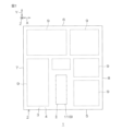
- FIG. 1 is a schematic plan view of a semiconductor device according to an embodiment of the present invention.
- FIG. 2 is an enlarged view of region II shown in FIG.
- FIG. 3 is a perspective view of the gate electrode in FIG.
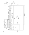
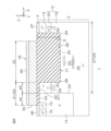
- FIG. 4 is a schematic perspective view of an LDMOSFET.
- FIG. 5 is a cross-sectional view taken along line VV shown in FIG.
- FIG. 6 is a cross-sectional view taken along the line VI-VI shown in FIG.
- FIG. 7 is a diagram showing a state in which a current flows through the first active area.
- FIG. 8 is a diagram showing a state in which a current flows through the second active area.
- FIG. 9 is a diagram showing an example of a characteristic structure that can be introduced into the semiconductor device.
- FIG. 9 is a diagram showing an example of a characteristic structure that can be introduced into the semiconductor device.
- FIG. 10 is a diagram showing an example of a characteristic structure that can be introduced into the semiconductor device.
- FIG. 11 is a diagram showing an example of a characteristic structure that can be introduced into the semiconductor device.
- FIG. 12 is a diagram showing an example of a characteristic structure that can be introduced into the semiconductor device.
- FIG. 13 is a diagram showing an example of a characteristic structure that can be introduced into the semiconductor device.
- FIG. 14 is a diagram showing an example of a characteristic structure that can be introduced into the semiconductor device.
- FIG. 15 is a diagram showing an example of a characteristic structure that can be introduced into the semiconductor device.
- FIG. 16 is a diagram showing an example of a characteristic structure that can be introduced into the semiconductor device.
- FIG. 17 is a diagram showing an example of a characteristic structure that can be introduced into the semiconductor device.
- FIG. 18 is a diagram showing an example of a characteristic structure that can be introduced into the semiconductor device.
- FIG. 19 is a diagram showing an example of a characteristic structure that can be introduced into the semiconductor device.
- FIG. 20 is a diagram showing an example of a characteristic structure that can be introduced into the semiconductor device.
- FIG. 21 is a diagram showing an example of a characteristic structure that can be introduced into the semiconductor device.
- FIG. 22 is a diagram showing an example of a characteristic structure that can be introduced into the semiconductor device.
- FIG. 23 is a diagram showing an example of a characteristic structure that can be introduced into the semiconductor device.
- FIG. 24 is a diagram showing an example of a characteristic structure that can be introduced into the semiconductor device.
- FIG. 1 is a schematic plan view of a semiconductor device 1 according to one embodiment of the present invention.
- the semiconductor device 1 includes a semiconductor chip 2 formed in a rectangular parallelepiped shape.
- the semiconductor chip 2 forms the outer shape of the semiconductor device 1, and is, for example, a structure in which a single crystal semiconductor material is formed into a chip shape (rectangular parallelepiped shape).
- the semiconductor chip 2 is formed from a semiconductor material such as Si or SiC.
- the semiconductor chip 2 has a first main surface 3 on one side, a second main surface 4 on the other side, and first to fourth side surfaces 5 to 8 connecting the first main surface 3 and the second main surface 4.
- the first to fourth side surfaces 5 to 8 include a first side surface 5, a second side surface 6, a third side surface 7, and a fourth side surface 8.
- the first side surface 5 and the second side surface 6 extend in a first direction X and face a second direction Y that is perpendicular to the first direction X.
- the third side surface 7 and the fourth side surface 8 extend in the second direction Y and face the first direction X.
- the first main surface 3 and the second main surface 4 are formed in a quadrangular shape in a plan view (hereinafter simply referred to as "plan view") seen from the third direction Z (the normal direction of the first main surface 3 and the second main surface 4).
- the first main surface 3 may be referred to as a device surface on which functional devices are formed.
- the second main surface 4 may be referred to as a non-device surface on which no functional devices are formed.
- a plurality of device regions 9 are formed on the first main surface 3. The number and arrangement of the plurality of device regions 9 are arbitrary.
- the plurality of device regions 9 may include functional devices formed by utilizing the surface layer portion of the first main surface 3.
- the functional devices may include, for example, at least one of a semiconductor switching device, a semiconductor rectifying device, and a passive device.
- the functional devices may include, for example, a circuit network in which at least two of a semiconductor switching device, a semiconductor rectifying device, and a passive device are combined.
- the semiconductor switching devices may include, for example, at least one of a Metal Oxide Semiconductor Field Effect Transistor (MOSFET), a Bipolar Junction Transistor (BJT), an Insulated Gate Bipolar Junction Transistor (IGBT) and a Junction Field Effect Transistor (JFET).
- MOSFET Metal Oxide Semiconductor Field Effect Transistor
- BJT Bipolar Junction Transistor
- IGBT Insulated Gate Bipolar Junction Transistor
- JFET Junction Field Effect Transistor
- the semiconductor rectifying devices may include, for example, at least one of a pn junction diode, a pin junction diode, a Zener diode, a Schottky barrier diode and a fast recovery diode.
- the passive devices may include, for example, at least one of a resistor, a capacitor and an inductor.
- FIG. 2 is an enlarged view of region II shown in FIG. 1.
- FIG. 3 is a perspective view of gate conductor 18 in FIG. 2. For clarity, gate conductor 18 is shown hatched in FIGS. 2 and 3, and insulating isolation structure 17 is shown filled in gray.
- the semiconductor device 1 has an LDMOS region 11 among a plurality of device regions 9 in which an LDMOSFET 10 (Lateral Double Diffused MOSFET) is formed.
- LDMOSFET 10 Longer Double Diffused MOSFET
- the LDMOS region 11 includes a drift region 12, a drain region 13, a body region 14, a source region 15, a body contact region 16, an insulating isolation structure 17, and a gate conductor 18.
- the drift region 12 is a diffusion region of n-type impurities.
- the drift region 12 may also be referred to as an n-type drift region.
- the drift region 12 is a region that reduces the surface electric field in the LDMOSFET 10, and may also be referred to as an n-type RESURF (REduced SURface Field) layer.
- the drift region 12 is formed over the entire surface portion of the first main surface 3 of the semiconductor chip 2.
- the drift region 12 includes a first drift region 19 and a second drift region 20.
- the first drift region 19 is formed over the entire surface portion of the first main surface 3, and the second drift region 20 is selectively formed in the surface portion of the first drift region 19.
- the second drift region 20 is formed in the first drift region 19 in the shape of a well, and may therefore be referred to as an n-type well region.
- the n-type impurity concentration of first drift region 19 may be, for example, not less than 1.0 ⁇ 10 14 cm -3 and not more than 1.0 ⁇ 10 16 cm -3 .
- the n-type impurity concentration of second drift region 20 is higher than the n-type impurity concentration of first drift region 19.
- the n-type impurity concentration of second drift region 20 may be, for example, not less than 1.0 ⁇ 10 15 cm -3 and not more than 1.0 ⁇ 10 17 cm -3 .
- the first drift region 19 may be referred to as a low-concentration drift region (low-concentration resurf layer) in its relative relationship with the second drift region 20.
- the second drift region 20 may be referred to as a high-concentration drift region (high-concentration resurf layer) in its relative relationship with the first drift region 19.
- the first drift region 19 and the second drift region 20 may be referred to as a high-resistance drift region and a low-resistance drift region, respectively.
- the body region 14 is a p-type impurity diffusion region.
- the body region 14 may be referred to as a p-type body region.
- the body region 14 is formed at a distance from the pair of drain regions 13.
- the body region 14 is formed in a region sandwiched between the pair of drain regions 13.
- the body region 14 may be surrounded by the second drift region 20.
- the body region 14 is in contact with the second drift region 20 and forms a boundary 22 with the second drift region 20, but may be formed at a distance inward from the second drift region 20.
- a part of the first drift region 19 may be formed between the body region 14 and the second drift region 20.
- the body region 14 is formed in the first drift region 19 in a well shape, so may be referred to as a p-type well region.
- the source region 15 is an n-type impurity diffusion region having a higher n-type impurity concentration than the drift region 12.
- the source region 15 may be referred to as an n-type source region.
- the n-type impurity concentration of the source region 15 may be, for example, not less than 1.0 ⁇ 10 16 cm ⁇ 3 and not more than 5.0 ⁇ 10 17 cm ⁇ 3 .
- the source region 15 is formed in the surface layer of the body region 14.
- the source region 15 is formed in an inner region of the body region 14 spaced inward from the outer periphery of the body region 14.
- the annular region between the source region 15 and the body region 14 in plan view is a channel region 23 in which the channel of the LDMOSFET 10 is formed.
- the source region 15 is formed in a band shape extending along the second direction Y in plan view.
- the body contact region 16 is a diffusion region of p-type impurities having a higher p-type impurity concentration than the body region 14.
- the body contact region 16 may be referred to as a p-type body contact region.
- the p-type impurity concentration of the body contact region 16 may be, for example, not less than 1.0 ⁇ 10 16 cm ⁇ 3 and not more than 5.0 ⁇ 10 17 cm ⁇ 3 .
- the body contact region 16 is formed in the surface layer of the body region 14.
- the body contact region 16 is formed in an inner region of the source region 15 spaced inward from the outer periphery of the source region 15.
- the body contact region 16 is formed in a band shape extending along the second direction Y in a plan view.
- source contacts 24 connected to the source region 15 and the body contact region 16 are formed in the source region 15 and the body contact region 16.
- a plurality of source contacts 24 are arranged at intervals in the second direction Y.
- Each source contact 24 straddles the source region 15 and the body contact region 16 and is connected to both the source region 15 and the body contact region 16.
- the region sandwiched between the body region 14 and the drain region 13 in the first direction X is the active region 25 through which the current of the LDMOSFET 10 flows.
- the insulating isolation structure 17 is formed in the active region 25.
- a plurality of insulating isolation structures 17 are arranged at intervals in the second direction Y.
- the active region 25 may be separated into a first active area 26 sandwiched between adjacent insulating isolation structures 17 and a second active area 27 covered by each insulating isolation structure 17.
- a plurality of first active areas 26 and a plurality of second active areas 27 are arranged alternately in the second direction Y.
- the plurality of insulating isolation structures 17 are physically separated and independent from one another.
- Each insulating isolation structure 17 is formed in a band shape that crosses the active region 25 in the first direction X from the body region 14 toward the drain region 13. More specifically, it is formed in a rectangular shape having a long side along the first direction X and a short side along the second direction Y. As a result, the first active area 26 has a constant width W1 in the second direction Y. Furthermore, the second active area 27 (insulating isolation structure 17) has a constant width W2 in the second direction Y.
- the width W1 may be narrower than the width W2.
- the width W1 may be 0.1 ⁇ m or more and 5 ⁇ m or less, and the width W2 may be 0.2 ⁇ m or more and 2 ⁇ m or less.
- each insulating isolation structure 17 has a first end 28 in the first direction X and a second end 29 on the opposite side.
- the first end 28 is an end on the body region 14 side (source region 15 side).
- the first end 28 may be spaced apart from the body region 14 in the first direction X and face the body region 14 with a part of the second drift region 20 in between.
- the second end 29 is an end on the drain region 13 side.
- the second end 29 may be in contact with the drain region 13.
- the first end 28 may be in contact with the body region 14, and the second end 29 may be spaced apart from the drain region 13 in the first direction X and face the body region 14 with a part of the second drift region 20 in between.
- the gate conductor 18 is formed in a ring shape surrounding the source region 15 and the body contact region 16 in a plan view. For clarity, the gate conductor 18 is shown hatched in FIG. 2.
- a source opening 30 exposing the source region 15 and the body contact region 16 is formed in the center of the gate conductor 18.
- the source opening 30 is formed in an elongated shape along the second direction Y, and integrally exposes the source region 15 and the body contact region 16.
- the gate conductor 18 includes a gate electrode 31 that covers the channel region 23 and a gate field plate 32 that extends integrally from the gate electrode 31.
- the gate electrode 31 covers, from the inside to the outside, the source region 15, the channel region 23 (body region 14), and the second drift region 20.
- the gate electrode 31 includes a pair of control parts 33 that face each other with a gap in the first direction X across the source opening 30, and a pair of contact parts 34 that connect both ends of the pair of control parts 33 in the second direction Y.
- a pair of island-shaped contact portions 34 are integrally connected to both ends of a pair of linear control portions 33 that are parallel to each other along the second direction Y.
- Each contact portion 34 protrudes outward in the first direction X relative to the pair of control portions 33, and is formed wider than the pair of control portions 33.
- each control portion 33 is set back inward relative to the edge of each contact portion 34 in the first direction X.
- a recess 35 adjacent to each control portion 33 is formed between the pair of contact portions 34 in the second direction Y.
- a gate contact 36 to which a gate voltage is applied is formed in the contact portion 34.
- a plurality of gate contacts 36 are arranged at intervals in the first direction X.
- the gate field plate 32 extends from the gate electrode 31 to a region above the insulating isolation structure 17.
- the multiple gate field plates 32 are arranged at intervals in the second direction Y.
- the multiple gate field plates 32 are collectively formed in a comb-like shape protruding from the gate electrode 31 to the opposite side of the source opening 30.
- Each gate field plate 32 is provided in a one-to-one relationship with each insulating isolation structure 17.
- a recess 35 is formed in the gate electrode 31, and some or all of the multiple gate field plates 32 are formed within the recess 35.
- the recess 35 can be effectively used as space for the gate field plates 32, thereby narrowing the overall width of the gate conductor 18 in the first direction X. This makes it possible to reduce the area of the active region 25.
- Each gate field plate 32 is formed in a band shape extending in the first direction X. More specifically, it is formed in a rectangular shape having a long side along the first direction X and a short side along the second direction Y. As a result, each gate field plate 32 has a constant width W3 in the second direction Y.
- the gate conductor 18 is made of polysilicon.
- the gate electrode 31 of the gate conductor 18 is made of n-type polysilicon
- the gate field plate 32 is made of i-type polysilicon.
- CVD chemical vapor deposition
- a gate conductor 18 with separated n-type and i-type portions can be formed.
- the gate electrode 31 and the gate field plate 32 may both be made of n-type polysilicon.
- the charge storage effect of the n-type polysilicon can reduce the on-resistance.
- the gate conductor 18 may have the gate electrode 31 formed from n-type polysilicon and the gate field plate 32 formed from p-type polysilicon.
- P-type polysilicon has a different work function from n-type polysilicon.
- the Fermi level of a p-type polysilicon gate is 1V lower than that of an n-type polysilicon gate by the band gap. Therefore, an extra 1V must be applied to bend the silicon side band.
- FIG. 4 is a schematic perspective view of LDMOSFET 10.
- FIG. 5 is a cross-sectional view taken along line V-V in FIG. 4.
- FIG. 6 is a cross-sectional view taken along line VI-VI in FIG. 4.
- FIG. 5 shows a cross-section of the first active area 26, and
- FIG. 6 shows a cross-section of the second active area 27.
- the drift region 12 is formed in the surface layer of the semiconductor chip 2.
- a first drift region 19 is formed as a base region, and a second drift region 20 is formed on the first drift region 19.
- a p-type region supporting the drift region 12 may be formed on the second main surface side of the semiconductor chip 2.
- the p-type region may be a p-type semiconductor substrate.
- the drift region 12 may be an n-type epitaxial layer.
- the thickness of the drift region 12 may be 5 ⁇ m or more and 20 ⁇ m or less.
- the drift region 12 is isolated into multiple regions by an element isolation structure (not shown, for example, an element isolation well, DTI (Deep Trench Isolation), STI (Shallow Trench Isolation), etc.).
- the element isolation structure divides the semiconductor chip 2 into multiple device regions 9.
- Figures 4 to 6 show the drift region 12 that forms the LDMOS region 11 out of the multiple separated drift regions 12.
- the drain region 13 is formed in the surface layer of the second drift region 20.
- the bottom of the drain region 13 is located closer to the first main surface 3 than the boundary between the first drift region 19 and the second drift region 20 in the third direction Z.
- a drain silicide 37 is formed on the first main surface 3 above the drain region 13.
- the body region 14 penetrates the second drift region 20 and reaches the first drift region 19.
- the source region 15 and the body contact region 16 are formed in the surface layer of the body region 14. The bottoms of the source region 15 and the body contact region 16 are located closer to the first main surface 3 than the boundary between the first drift region 19 and the body region 14 in the third direction Z.
- a source silicide 38 is formed on the first main surface 3 above the source region 15 and the body contact region 16.
- the insulating isolation structure 17 includes a trench 39 formed in the semiconductor chip 2 and a buried insulator 40 buried in the trench 39.
- the trench 39 penetrates the second drift region 20 from the first main surface 3 and reaches the first drift region 19.
- the trench 39 has a bottom at a position deeper than the boundary between the first drift region 19 and the second drift region 20.
- the buried insulator 40 is buried up to the opening end of the trench 39.
- the buried insulator 40 is formed of silicon oxide (SiO 2 ).
- the depth D of the trench 39 (the thickness of the insulating isolation structure 17) may be, for example, 0.1 ⁇ m or more and 1 ⁇ m or less.
- the isolation structure 17 is formed by a so-called STI (Shallow Trench Isolation) structure.
- the isolation structure 17 may be formed by a field insulating film such as a LOCOS film.
- the second active area 27 is formed by the first drift region 19 that extends directly below the isolation structure 17.
- a main surface insulating film 41 is formed on the first main surface 3.
- the main surface insulating film 41 entirely covers the first main surface 3.
- the main surface insulating film 41 is made of silicon oxide (SiO 2 ), but may be made of silicon nitride (SiN).
- the main surface insulating film 41 may include a gate insulating film 42 between the gate conductor 18 and the first main surface 3, and an active coating film 43 that covers the first active area 26.
- the gate insulating film 42 is sandwiched between the gate conductor 18 and the semiconductor chip 2.
- the gate insulating film 42 may include a first portion 44 between the gate conductor 18 and the body region 14 (channel region 23), and a second portion 45 between the gate conductor 18 and the drift region 12.
- the gate insulating film 42 may have a uniform thickness T1 throughout the first portion 44 and the second portion 45.
- the thickness T1 of the gate insulating film 42 is, for example, 2 nm or more and 50 nm or less.
- the active coating film 43 is a film that prevents silicidation of the first active area 26, and may be referred to as a silicide block film.
- the active coating film 43 may have a thickness T2 that is thicker than the thickness T1 of the gate insulating film 42, for example, not less than 10 nm and not more than 100 nm. With reference to FIG. 5, a portion of the active coating film 43 may partially cover the side and top surface of the gate conductor 18. In the portion covered by the active coating film 43, a gate silicide 46 is formed on the surface of the gate conductor 18.
- an interlayer film 47 is formed on the first main surface 3.
- the inside of the interlayer film 47 is shown in a see-through manner.
- the interlayer film 47 covers the gate conductor 18.
- the interlayer film 47 is made of silicon oxide (SiO 2 ), but may be made of silicon nitride (SiN).
- a drain wiring 48, a source wiring 49, and a gate wiring 50 are formed on the interlayer film 47.
- the drain wiring 48 is electrically connected to the drain region 13 via a drain contact 21 embedded in the interlayer film 47.
- the drain wiring 48 is formed in a strip shape that extends along the drain region 13 with the interlayer film 47 in between, and faces the drain region 13 in a straight line.
- the source wiring 49 is electrically connected to the source region 15 and the body contact region 16 via a source contact 24 embedded in the interlayer film 47.
- the source wiring 49 is formed in a strip shape that extends along the source region 15 with the interlayer film 47 in between, and faces the source region 15 in a straight line.
- the gate wiring 50 is electrically connected to the gate electrode 31 via a gate contact 36 embedded in the interlayer film 47.
- FIG. 4 shows the gate contact 36 connected to the control portion 33 of the gate electrode 31, the gate contact 36 may be connected to the contact portion 34 as shown in FIG. 2.
- the gate wiring 50 is formed in a strip shape extending along the gate electrode 31 with the interlayer film 47 in between.
- the gate wiring 50 may integrally include a gate covering portion 51 that covers the gate electrode 31 with the interlayer film 47 in between, and an active covering portion 52 that covers the active region 25 with the interlayer film 47 in between.
- the gate covering portion 51 is formed in a band shape extending along the gate electrode 31 with the interlayer film 47 in between, and faces the gate electrode 31 in a straight line.
- the active covering portion 52 extends across the first active area 26 and the second active area 27 (insulating isolation structure 17 and gate field plate 32) in the second direction Y, and faces the first active area 26 and the second active area 27 with the interlayer film 47 in between.
- the source region 15 and the body contact region 16 are grounded via the source wiring 49, and a positive voltage (drain voltage) is applied to the drain region 13. Then, by controlling the potential of the gate electrode 31, a channel is formed in the channel region 23 near the interface with the gate insulating film 42, allowing a drain current to flow between the source region 15 and the drain region 13.
- FIGS. 7 and 8 are diagrams showing how currents flow through the first active area 26 and the second active area 27, respectively.
- FIG. 7 is a cross-sectional view corresponding to FIG. 5
- FIG. 8 is a cross-sectional view corresponding to FIG. 6.
- the first drift region 19 has a first resistance value R1 according to its n-type impurity concentration.
- the second drift region 20 has a second resistance value R2 according to its n-type impurity concentration. Comparing the first resistance value R1 and the second resistance value R2, the second resistance value R2 is lower than the first resistance value R1. This is because the n-type impurity concentration of the second drift region 20 is lower than the n-type impurity concentration of the first drift region 19.
- the current path 53 between the source and drain is shorter than the current path 54 in the second active area 27.
- the current flows around the bottom of the insulating isolation structure 17, so the current path 54 between the source and drain is longer than the current path 53 in the first active area 26. Therefore, the current between the source and drain flows preferentially in the first active area 26 where the second drift region 20 sandwiched between multiple insulating isolation structures 17 is formed.
- the multiple insulating isolation structures 17 sandwich the first active area 26 from both sides, and an electric field confinement effect is in effect, so that a sufficient off-state breakdown voltage can be obtained even if the second drift region 20 of the first active area 26 is highly doped.
- the first active area 26, which has a relatively low breakdown voltage and through which current flows preferentially when on, and the high-breakdown-voltage second active area 27, through which current does not flow easily when on but which provides a high breakdown voltage when off, are alternately arranged in parallel.
- the on-resistance can be reduced, losses can be reduced and the chip area can also be reduced.
- the chip area By reducing the chip area, the number of chips that can be obtained per wafer can be increased, reducing costs.
- parasitic capacitance and parasitic inductance can be reduced, and signal delays can also be reduced.
- the gate wiring 50 has an active covering portion 52 that covers the active region 25 with the interlayer film 47 in between. This allows a capacitance to be formed between the active region 25 and the gate wiring 50, thereby reducing the on-resistance and improving the off-state breakdown voltage.
- the thickness T3 of the first portion 44 and the thickness T4 of the second portion 45 of the gate insulating film 42 may be different from each other.
- the thickness T4 of the second portion 45 is greater than the thickness T3 of the first portion 44.
- the thickness T4 is smaller than the thickness of the insulating isolation structure 17 (in this embodiment, the depth D of the trench 39), and is, for example, 10 nm or more and 100 nm or less.
- the thickness T3 is, for example, 2 nm or more and 50 nm or less.
- the thickness T4 of the second portion 45 on the drift region 12 thicker than the thickness T3 of the first portion 44 on the channel region 23 and thinner than the thickness of the insulating isolation structure 17 (in this embodiment, the depth D of the trench 39), it is possible to obtain a sufficient off-state breakdown voltage while suppressing an increase in on-state resistance.
- the first active area 26 may be formed in a tapered shape in which the width W1 in the second direction Y gradually narrows from the source region 15 toward the drain region 13 in a plan view.
- the second active area 27 (insulation isolation structure 17) may be formed in a tapered shape in which the width W2 in the second direction Y gradually narrows from the drain region 13 toward the source region 15 in a plan view.
- the first active area 26 may be formed in a tapered shape in which the width W1 in the second direction Y gradually narrows from the drain region 13 toward the source region 15 in a plan view.
- the second active area 27 (insulation isolation structure 17) may be formed in a tapered shape in which the width W2 in the second direction Y gradually narrows from the source region 15 toward the drain region 13 in a plan view.
- a sufficient off-state breakdown voltage can be obtained by narrowing the width of the first active area 26 on the source region 15 side, where the electric field is relatively more likely to concentrate than on the drain region 13 side.
- the pn junction is the junction between the n-type drain and the p-type body, and is located on the source region 15 side relative to the first active area 26 and the slit-shaped portion of the insulating isolation structure 17. Therefore, if the width W2 of the insulating isolation structure 17, which determines the off-state breakdown voltage, is wider on the source region 15 side (in other words, the width W1 of the first active area 26 is narrower on the source region 15 side), electric field concentration can be suppressed. As a result, the off-state breakdown voltage can be increased.
- the insulating isolation structure 17 may integrally include a first structure 55 and a second structure 56.
- the first structure 55 extends along the first direction X and sandwiches the first active area 26 in the second direction Y.
- the second structure 56 extends along the second direction Y and connects the first ends 28 of the pair of first structures 55 on the source region 15 side. In the adjacent first structures 55, the second ends 29 on the drain region 13 side are open.
- the first active area 26 is partitioned on three sides by the pair of first structures 55 and the second structure 56 connecting them. In this form, a sufficient off-state breakdown voltage can be obtained by blocking the first active area 26 on the source region 15 side, where the electric field is relatively more likely to concentrate than on the drain region 13 side, with the second structure 56.
- the insulating isolation structure 17 may integrally include a first structure 57 and a second structure 58.
- the first structure 57 extends along the first direction X and sandwiches the first active area 26 in the second direction Y.
- the second structure 58 extends along the second direction Y and connects the second ends 29 of the pair of first structures 57 on the drain region 13 side.
- the first ends 28 on the source region 15 side are open.
- the first active area 26 is partitioned on three sides by the pair of first structures 57 and the second structure 58 connecting them. In this form, a sufficient off-state breakdown voltage can be obtained by blocking the first active area 26 on the drain region 13 side, where the electric field is relatively less likely to spread compared to the source region 15 side, with the second structure 58.
- the drain region 13 may be sandwiched between adjacent insulating isolation structures 17, with both ends in the second direction Y in contact with the insulating isolation structures 17.
- the drain region 13 may be divided into multiple parts by multiple insulating isolation structures 17 crossing the band-shaped drain region 13 (see FIG. 3) in a plan view in the first direction X.
- part of the drain region 13 is replaced with the insulating isolation structures 17, reducing the area of the drain region 13, resulting in a higher on-resistance than the structure in FIG. 3.
- the electric field confinement effect from both sides of the first active area 26 in the second direction Y can be improved, thereby improving the off-state breakdown voltage.
- the gate field plate 32 may be formed in a tapered shape in which the width W3 in the second direction Y gradually narrows from the source region 15 toward the drain region 13 in a plan view.
- a sufficient off-state breakdown voltage can be obtained by widening the width of the gate field plate 32 on the source region 15 side, where the electric field is more likely to concentrate than on the drain region 13 side.
- the drain voltage is distributed from the drain to the source. If the gate field plate 32 at 0V is close to the first active area 26, it has the effect of pushing the electric field towards the first active area 26 and the drain region 13. As a result, the drain voltage is distributed more towards the drain side, causing the electric field to concentrate.
- the gate field plate 32 By making the gate field plate 32 into a thin wedge shape on the drain side and moving it away from the first active area 26 on the drain side, the electric field concentration can be alleviated, and the cut-off breakdown voltage can sometimes be increased.
- the gate field plate 32 may be formed in a tapered shape in which the width W3 in the second direction Y gradually narrows from the drain region 13 toward the source region 15 in a plan view.
- a sufficient off-state breakdown voltage can be obtained by widening the width of the gate field plate 32 on the drain region 13 side, where the electric field is relatively less likely to spread compared to the source region 15 side.
- the gate field plate 32 can be shaped like a thin wedge on the source side, moving it away from the first active area 26 on the source side, thereby mitigating the electric field relaxation, which may increase the breakdown voltage.
- the semiconductor device 1 may further include a floating field plate 59 formed on the first active area 26 and in an electrically floating state.
- a floating field plate 59 formed on the first active area 26 and in an electrically floating state.
- a plurality of floating field plates 59 are formed, one on each of the first active areas 26.
- the gate field plates 32 and the floating field plates 59 are arranged alternately at intervals in the second direction Y.
- Each floating field plate 59 is formed in a band shape extending in the first direction X. More specifically, it is formed in a rectangular shape having a long side along the first direction X and a short side along the second direction Y. As a result, each floating field plate 59 has a constant width in the second direction Y. As shown in FIG. 17, each floating field plate 59 may be formed only inside the first active area 26 and the boundary between the first active area 26 and the insulating isolation structure 17, or may cross the boundary between the first active area 26 and the insulating isolation structure 17 and partially cover the insulating isolation structure 17.
- the floating field plate 59 is disposed on the first active area 26, which can reduce the electric field concentration on the surface layer of the first active area 26. This can improve the off-state breakdown voltage.
- the semiconductor device 1 may further include a floating field plate 60 that extends across the first active area 26 and the insulating isolation structure 17 (second active area 27) in the second direction Y and is in an electrically floating state.
- a plurality of floating field plates 60 are arranged at intervals in the first direction X.
- Each floating field plate 60 is formed in a band shape extending in the second direction Y. More specifically, it is formed in a rectangular shape having a long side along the second direction Y and a short side along the first direction X. As a result, each floating field plate 60 has a constant width in the first direction X. As shown in FIG. 18, each floating field plate 60 may continuously cross a plurality of first active areas 26 and a plurality of insulating isolation structures 17, or may simply cross the boundary between one first active area 26 and one insulating isolation structure 17.
- the drift region 12 (in this embodiment, the second drift region 20) has protrusions 61 that selectively protrude from the first active area 26 toward the body region 14 in the first direction X.
- a plurality of protrusions 61 are arranged at intervals in the second direction Y, and one protrusion 61 protrudes from each first active area 26.
- the boundary 22 between the body region 14 and the second drift region 20 is formed in a zigzag shape that is convex toward the source region 15 in the section adjacent to the first active area 26 and convex toward the drain region 13 in the section adjacent to the insulating isolation structure 17.
- the zigzag of the boundary 22 may be formed in a pulse waveform shape as shown in FIG. 19, or in a sine curve shape.
- the drift region 12 (in this embodiment, the second drift region 20) has recesses 62 selectively recessed in the first direction X from the body region 14 toward the first active area 26.
- a plurality of recesses 62 are arranged at intervals in the second direction Y, with one recess 62 facing each of the first active areas 26.
- the boundary 22 between the body region 14 and the second drift region 20 is formed in a zigzag shape that is concave toward the drain region 13 in the section adjacent to the first active area 26 and convex toward the source region 15 in the section adjacent to the insulating isolation structure 17.
- the zigzag of the boundary 22 may be formed in a pulse waveform shape as shown in FIG. 20, or in a sine curve shape.
- the second drift region 20 may include a plurality of first diffusion regions 63 and a plurality of second diffusion regions 64 arranged in an alternating stripe pattern in the second direction Y.
- the plurality of first diffusion regions 63 may have a higher n-type impurity concentration than the plurality of second diffusion regions 64.
- the plurality of first diffusion regions 63 and the plurality of second diffusion regions 64 are arranged alternately in the second direction Y.
- n-type impurities are selectively injected into the region in the first drift region 19 where the first diffusion region 63 is to be formed, and then annealing is performed. This causes the impurities to diffuse laterally from the first diffusion region 63 along the first main surface 3. As a result, a second diffusion region 64 can be formed that has a lower impurity concentration than the first diffusion region 63 and a higher impurity concentration than the first drift region 19.
- a mask for an existing diffusion layer with a stripe pattern can be used instead, eliminating the need for a dedicated mask for the second drift region 20. This reduces manufacturing costs.
- the impurity concentration in the second diffusion region 64 can also be adjusted.
- the second drift region 20 may include a plurality of first diffusion regions 65 and a plurality of second diffusion regions 66 arranged in an alternating striped pattern in the first direction X.
- the plurality of first diffusion regions 65 may have a higher n-type impurity concentration than the plurality of second diffusion regions 66.
- the plurality of first diffusion regions 65 and the plurality of second diffusion regions 66 are arranged alternately in the first direction Y.
- n-type impurities are selectively injected into the region in the first drift region 19 where the first diffusion region 65 is to be formed, and then annealing is performed. This causes the impurities to diffuse laterally from the first diffusion region 65 along the first main surface 3.
- a second diffusion region 66 can be formed that has a lower impurity concentration than the first diffusion region 65 and a higher impurity concentration than the first drift region 19.
- a mask for an existing diffusion layer with a stripe pattern can be used instead, eliminating the need for a dedicated mask for the second drift region 20. This reduces manufacturing costs.
- the impurity concentration in the second diffusion region 66 can also be adjusted.
- the semiconductor device 1 may further include a p-type top diffusion region 67 selectively formed in the surface layer of the second drift region 20 in the first active area 26.
- the top diffusion region 67 is formed away from the bottom and sides of the second drift region 20 (the boundary 22 with the body region 14) and in a floating state in the second drift region 20.
- the top diffusion region 67 is covered by the active coating film 43 and is physically separated from the drain contact 21, the source contact 24, and the gate contact 36.
- a p-type top diffusion region 67 is formed in the second drift region 20. This allows the depletion layer to expand from the pn junction between the top diffusion region 67 (p-type) and the second drift region 20 (n-type). This promotes electric field relaxation in the second drift region 20, which has a higher n-type impurity concentration than the first drift region 19, and improves the off-state breakdown voltage.
- manufacturing costs can also be reduced.
- a plurality of source regions 15 and a plurality of body contact regions 16 are arranged alternately in the second direction Y. More specifically, in the body region 14, the source region 15 is formed in a section adjacent to the first active area 26, and the body contact region 16 is formed in a section adjacent to the insulating isolation structure 17.
- the plurality of source contacts 24 are connected to each of the plurality of source regions 15. Therefore, each source contact 24 is disposed at a position adjacent to the first active area 26 in the first direction X.
- both the source region 15 and the source contact 24 are adjacent to the first active area 26 in the first direction X.
- the source contact 24, the first active area 26, and the drain contact 21 are aligned in a straight line in the first direction X, allowing a current to flow between the source and drain via a short current path 68.
- the first conductivity type was n-type and the second conductivity type was p-type, but the first conductivity type may be p-type and the second conductivity type may be n-type.
- a specific configuration in this case can be obtained by replacing the n-type regions with p-type regions and the p-type regions with n-type regions in the above description and the attached drawings.
- a semiconductor chip (2) having a main surface (3); a drift region (12) of a first conductivity type formed in a surface layer portion of the main surface (3) of the semiconductor chip (2); a drain region (13) of a first conductivity type formed in a surface layer portion of the drift region (12); a body region (14) of a second conductivity type formed in a surface layer portion of the drift region (12) and spaced apart from the drain region (13) in a first direction (X); a first conductivity type source region (15) formed in a surface layer portion of the body region (14); a gate insulating film (42) formed on the main surface (3) of the semiconductor chip (2); a gate electrode (31) formed on the gate insulating film (42) and facing a channel region (23) formed in the body region (14); a plurality of insulating isolation structures (17) embedded in a surface layer of the main surface (3) of the semiconductor chip (2) along the first direction (X) between the body region (14) and the drain region (13); a first active area (26) sandwiched between
- a semiconductor chip (2) having a main surface (3); a drift region (12) of a first conductivity type formed in a surface layer portion of the main surface (3) of the semiconductor chip (2); a drain region (13) of a first conductivity type formed in a surface layer portion of the drift region (12); a body region (14) of a second conductivity type formed in a surface layer portion of the drift region (12) and spaced apart from the drain region (13) in a first direction (X); a first conductivity type source region (15) formed in a surface layer portion of the body region (14); a gate insulating film (42) formed on the main surface (3) of the semiconductor chip (2); a gate electrode (31) formed on the gate insulating film (42) and facing a channel region (23) formed in the body region (14); a plurality of insulating isolation structures (17) embedded in a surface layer of the main surface (3) of the semiconductor chip (2) along the first direction (X) between the body region (14) and the drain region (13); a first active area (26) sandwiched between
- a semiconductor chip (2) having a main surface (3); a drift region (12) of a first conductivity type formed in a surface layer portion of the main surface (3) of the semiconductor chip (2); a drain region (13) of a first conductivity type formed in a surface layer portion of the drift region (12); a body region (14) of a second conductivity type formed in a surface layer portion of the drift region (12) and spaced apart from the drain region (13) in a first direction (X); a first conductivity type source region (15) formed in a surface layer portion of the body region (14); a gate insulating film (42) formed on the main surface (3) of the semiconductor chip (2); a gate electrode (31) formed on the gate insulating film (42) and facing a channel region (23) formed in the body region (14); a plurality of insulating isolation structures (17) embedded in a surface layer of the main surface (3) of the semiconductor chip (2) along the first direction (X) between the body region (14) and the drain region (13); a first active area (26) sandwiched between
- a semiconductor chip (2) having a main surface (3); a drift region (12) of a first conductivity type formed in a surface layer portion of the main surface (3) of the semiconductor chip (2); a drain region (13) of a first conductivity type formed in a surface layer portion of the drift region (12); a body region (14) of a second conductivity type formed in a surface layer portion of the drift region (12) and spaced apart from the drain region (13) in a first direction (X); a first conductivity type source region (15) formed in a surface layer portion of the body region (14); a gate insulating film (42) formed on the main surface (3) of the semiconductor chip (2); a gate electrode (31) formed on the gate insulating film (42) and facing a channel region (23) formed in the body region (14); a plurality of insulating isolation structures (17) embedded in a surface layer of the main surface (3) of the semiconductor chip (2) along the first direction (X) between the body region (14) and the drain region (13); a first active area (26) sandwiched between
- a semiconductor chip (2) having a main surface (3); a drift region (12) of a first conductivity type formed in a surface layer portion of the main surface (3) of the semiconductor chip (2); a drain region (13) of a first conductivity type formed in a surface layer portion of the drift region (12); a body region (14) of a second conductivity type formed in a surface layer portion of the drift region (12) and spaced apart from the drain region (13) in a first direction (X); a first conductivity type source region (15) formed in a surface layer portion of the body region (14); a gate insulating film (42) formed on the main surface (3) of the semiconductor chip (2); a gate electrode (31) formed on the gate insulating film (42) and facing a channel region (23) formed in the body region (14); a plurality of insulating isolation structures (17) embedded in a surface layer of the main surface (3) of the semiconductor chip (2) along the first direction (X) between the body region (14) and the drain region (13); a first active area (26) sandwiched between
- a semiconductor chip (2) having a main surface (3); a drift region (12) of a first conductivity type formed in a surface layer portion of the main surface (3) of the semiconductor chip (2); a drain region (13) of a first conductivity type formed in a surface layer portion of the drift region (12); a body region (14) of a second conductivity type formed in a surface layer portion of the drift region (12) and spaced apart from the drain region (13) in a first direction (X); a first conductivity type source region (15) formed in a surface layer portion of the body region (14); a gate insulating film (42) formed on the main surface (3) of the semiconductor chip (2); a gate electrode (31) formed on the gate insulating film (42) and facing a channel region (23) formed in the body region (14); a plurality of insulating isolation structures (17) embedded in a surface layer of the main surface (3) of the semiconductor chip (2) along the first direction (X) between the body region (14) and the drain region (13); a first active area (26) sandwiched between
- Appendix 1-7 The semiconductor device (1) according to any one of Appendices 1-1 to 1-6, wherein the insulating isolation structure (17) includes a trench (39) formed in the semiconductor chip (2) and a buried insulator (40) buried in the trench (39).
- the drift region (12) includes a first drift region (19) having a first impurity concentration, and a second drift region (20) formed on the first drift region (19) and having a second impurity concentration higher than the first impurity concentration;
- a semiconductor chip (2) having a main surface (3); a drift region (12) of a first conductivity type formed in a surface layer portion of the main surface (3) of the semiconductor chip (2); a drain region (13) of a first conductivity type formed in a surface layer portion of the drift region (12); a body region (14) of a second conductivity type formed in a surface layer portion of the drift region (12) and spaced apart from the drain region (13) in a first direction (X); a first conductivity type source region (15) formed in a surface layer portion of the body region (14); a gate insulating film (42) formed on the main surface (3) of the semiconductor chip (2); a gate electrode (31) formed on the gate insulating film (42) and facing a channel region (23) formed in the body region (14); a plurality of insulating isolation structures (17) embedded in a surface layer of the main surface (3) of the semiconductor chip (2) along the first direction (X) between the body region (14) and the drain region (13); a first active area (26) sandwiched between
- a semiconductor chip (2) having a main surface (3); a drift region (12) of a first conductivity type formed in a surface layer portion of the main surface (3) of the semiconductor chip (2); a drain region (13) of a first conductivity type formed in a surface layer portion of the drift region (12); a body region (14) of a second conductivity type formed in a surface layer portion of the drift region (12) and spaced apart from the drain region (13) in a first direction (X); a first conductivity type source region (15) formed in a surface layer portion of the body region (14); a gate insulating film (42) formed on the main surface (3) of the semiconductor chip (2); a gate electrode (31) formed on the gate insulating film (42) and facing a channel region (23) formed in the body region (14); a plurality of insulating isolation structures (17) embedded in a surface layer of the main surface (3) of the semiconductor chip (2) along the first direction (X) between the body region (14) and the drain region (13); a first active area (26) sandwiched between
- a semiconductor chip (2) having a main surface (3); a drift region (12) of a first conductivity type formed in a surface layer portion of the main surface (3) of the semiconductor chip (2); a drain region (13) of a first conductivity type formed in a surface layer portion of the drift region (12); a body region (14) of a second conductivity type formed in a surface layer portion of the drift region (12) and spaced apart from the drain region (13) in a first direction (X); a first conductivity type source region (15) formed in a surface layer portion of the body region (14); a gate insulating film (42) formed on the main surface (3) of the semiconductor chip (2); a gate electrode (31) formed on the gate insulating film (42) and facing a channel region (23) formed in the body region (14); a plurality of insulating isolation structures (17) embedded in a surface layer of the main surface (3) of the semiconductor chip (2) along the first direction (X) between the body region (14) and the drain region (13); a first active area (26) sandwiched between
- a semiconductor chip (2) having a main surface (3); a drift region (12) of a first conductivity type formed in a surface layer portion of the main surface (3) of the semiconductor chip (2); a drain region (13) of a first conductivity type formed in a surface layer portion of the drift region (12); a body region (14) of a second conductivity type formed in a surface layer portion of the drift region (12) and spaced apart from the drain region (13) in a first direction (X); a first conductivity type source region (15) formed in a surface layer portion of the body region (14); a gate insulating film (42) formed on the main surface (3) of the semiconductor chip (2); a gate electrode (31) formed on the gate insulating film (42) and facing a channel region (23) formed in the body region (14); a plurality of insulating isolation structures (17) embedded in a surface layer of the main surface (3) of the semiconductor chip (2) along the first direction (X) between the body region (14) and the drain region (13); a first active area (26) sandwiched between
- a semiconductor chip (2) having a main surface (3); a drift region (12) of a first conductivity type formed in a surface layer portion of the main surface (3) of the semiconductor chip (2); a drain region (13) of a first conductivity type formed in a surface layer portion of the drift region (12); a body region (14) of a second conductivity type formed in a surface layer portion of the drift region (12) and spaced apart from the drain region (13) in a first direction (X); a first conductivity type source region (15) formed in a surface layer portion of the body region (14); a gate insulating film (42) formed on the main surface (3) of the semiconductor chip (2); a gate electrode (31) formed on the gate insulating film (42) and facing a channel region (23) formed in the body region (14); a plurality of insulating isolation structures (17) embedded in a surface layer of the main surface (3) of the semiconductor chip (2) along the first direction (X) between the body region (14) and the drain region (13); a first active area (26) sandwiched between
- a semiconductor chip (2) having a main surface (3); a drift region (12) of a first conductivity type formed in a surface layer portion of the main surface (3) of the semiconductor chip (2); a drain region (13) of a first conductivity type formed in a surface layer portion of the drift region (12); a body region (14) of a second conductivity type formed in a surface layer portion of the drift region (12) and spaced apart from the drain region (13) in a first direction (X); a first conductivity type source region (15) formed in a surface layer portion of the body region (14); a gate insulating film (42) formed on the main surface (3) of the semiconductor chip (2); a gate electrode (31) formed on the gate insulating film (42) and facing a channel region (23) formed in the body region (14); a plurality of insulating isolation structures (17) embedded in a surface layer of the main surface (3) of the semiconductor chip (2) along the first direction (X) between the body region (14) and the drain region (13); a first active area (26) sandwiched between
- a semiconductor chip (2) having a main surface (3); a drift region (12) of a first conductivity type formed in a surface layer portion of the main surface (3) of the semiconductor chip (2); a drain region (13) of a first conductivity type formed in a surface layer portion of the drift region (12); a body region (14) of a second conductivity type formed in a surface layer portion of the drift region (12) and spaced apart from the drain region (13) in a first direction (X); a first conductivity type source region (15) formed in a surface layer portion of the body region (14); a gate insulating film (42) formed on the main surface (3) of the semiconductor chip (2); a gate electrode (31) formed on the gate insulating film (42) and facing a channel region (23) formed in the body region (14); a plurality of insulating isolation structures (17) embedded in a surface layer of the main surface (3) of the semiconductor chip (2) along the first direction (X) between the body region (14) and the drain region (13); a first active area (26) sandwiched between
- the drift region (12) includes a first drift region (19) having a first impurity concentration, and a second drift region (20) formed on the first drift region (19) and having a second impurity concentration higher than the first impurity concentration;
- a semiconductor chip (2) having a main surface (3); a drift region (12) of a first conductivity type formed in a surface layer portion of the main surface (3) of the semiconductor chip (2); a drain region (13) of a first conductivity type formed in a surface layer portion of the drift region (12); a body region (14) of a second conductivity type formed in a surface layer portion of the drift region (12) and spaced apart from the drain region (13) in a first direction (X); a first conductivity type source region (15) formed in a surface layer portion of the body region (14); a gate insulating film (42) formed on the main surface (3) of the semiconductor chip (2); a gate electrode (31) formed on the gate insulating film (42) and facing a channel region (23) formed in the body region (14); a plurality of insulating isolation structures (17) embedded in a surface layer of the main surface (3) of the semiconductor chip (2) along the first direction (X) between the body region (14) and the drain region (13); a first active area (26) sandwiched between
- a semiconductor chip (2) having a main surface (3); a drift region (12) of a first conductivity type formed in a surface layer portion of the main surface (3) of the semiconductor chip (2); a drain region (13) of a first conductivity type formed in a surface layer portion of the drift region (12); a body region (14) of a second conductivity type formed in a surface layer portion of the drift region (12) and spaced apart from the drain region (13) in a first direction (X); a first conductivity type source region (15) formed in a surface layer portion of the body region (14); a gate insulating film (42) formed on the main surface (3) of the semiconductor chip (2); a gate electrode (31) formed on the gate insulating film (42) and facing a channel region (23) formed in the body region (14); a plurality of insulating isolation structures (17) embedded in a surface layer of the main surface (3) of the semiconductor chip (2) along the first direction (X) between the body region (14) and the drain region (13); a first active area (26) sandwiched between
- a semiconductor chip (2) having a main surface (3); a drift region (12) of a first conductivity type formed in a surface layer portion of the main surface (3) of the semiconductor chip (2); a drain region (13) of a first conductivity type formed in a surface layer portion of the drift region (12); a body region (14) of a second conductivity type formed in a surface layer portion of the drift region (12) and spaced apart from the drain region (13) in a first direction (X); a first conductivity type source region (15) formed in a surface layer portion of the body region (14); a gate insulating film (42) formed on the main surface (3) of the semiconductor chip (2); a gate electrode (31) formed on the gate insulating film (42) and facing a channel region (23) formed in the body region (14); a plurality of insulating isolation structures (17) embedded in a surface layer of the main surface (3) of the semiconductor chip (2) along the first direction (X) between the body region (14) and the drain region (13); a first active area (26) sandwiched between
- a semiconductor chip (2) having a main surface (3); a drift region (12) of a first conductivity type formed in a surface layer portion of the main surface (3) of the semiconductor chip (2); a drain region (13) of a first conductivity type formed in a surface layer portion of the drift region (12); a body region (14) of a second conductivity type formed in a surface layer portion of the drift region (12) and spaced apart from the drain region (13) in a first direction (X); a first conductivity type source region (15) formed in a surface layer portion of the body region (14); a gate insulating film (42) formed on the main surface (3) of the semiconductor chip (2); a gate electrode (31) formed on the gate insulating film (42) and facing a channel region (23) formed in the body region (14); a plurality of insulating isolation structures (17) embedded in a surface layer of the main surface (3) of the semiconductor chip (2) along the first direction (X) between the body region (14) and the drain region (13); a first active area (26) sandwiched between
- a semiconductor chip (2) having a main surface (3); a drift region (12) of a first conductivity type formed in a surface layer portion of the main surface (3) of the semiconductor chip (2); a drain region (13) of a first conductivity type formed in a surface layer portion of the drift region (12); a body region (14) of a second conductivity type formed in a surface layer portion of the drift region (12) and spaced apart from the drain region (13) in a first direction (X); a first conductivity type source region (15) formed in a surface layer portion of the body region (14); a gate insulating film (42) formed on the main surface (3) of the semiconductor chip (2); a gate electrode (31) formed on the gate insulating film (42) and facing a channel region (23) formed in the body region (14); a plurality of insulating isolation structures (17) embedded in a surface layer of the main surface (3) of the semiconductor chip (2) along the first direction (X) between the body region (14) and the drain region (13); a first active area (26) sandwiched between
- the drift region (12) includes a first drift region (19) having a first impurity concentration, and a second drift region (20) formed on the first drift region (19) and having a second impurity concentration higher than the first impurity concentration;
- Appendix 3-8 The semiconductor device (1) according to any one of Appendix 3-1 to Appendix 3-5, wherein a plurality of the first active areas (26) and a plurality of the insulating isolation structures (17) are alternately arranged in the second direction (Y).
- a semiconductor chip (2) having a main surface (3); a drift region (12) of a first conductivity type formed in a surface layer portion of the main surface (3) of the semiconductor chip (2); a drain region (13) of a first conductivity type formed in a surface layer portion of the drift region (12); a body region (14) of a second conductivity type formed in a surface layer portion of the drift region (12) and spaced apart from the drain region (13) in a first direction (X); a first conductivity type source region (15) formed in a surface layer portion of the body region (14); a body contact region (16) of a second conductivity type formed at a terminal of the body region (14); a gate insulating film (42) formed on the main surface (3) of the semiconductor chip (2); a gate electrode (31) formed on the gate insulating film (42) and facing a channel region (23) formed in the body region (14); a plurality of insulating isolation structures (17) embedded in a surface layer of the main surface (3) of the semiconductor chip (2) along the first direction (
- a semiconductor chip (2) having a main surface (3); a drift region (12) of a first conductivity type formed in a surface layer portion of the main surface (3) of the semiconductor chip (2); a drain region (13) of a first conductivity type formed in a surface layer portion of the drift region (12); a body region (14) of a second conductivity type formed in a surface layer portion of the drift region (12) and spaced apart from the drain region (13) in a first direction (X); a first conductivity type source region (15) formed in a surface layer portion of the body region (14); a body contact region (16) of a second conductivity type formed at a terminal of the body region (14); a gate insulating film (42) formed on the main surface (3) of the semiconductor chip (2); a gate electrode (31) formed on the gate insulating film (42) and facing a channel region (23) formed in the body region (14); a plurality of insulating isolation structures (17) embedded in a surface layer of the main surface (3) of the semiconductor chip (2) along the first direction (
- the drift region (12) includes a first drift region (19) having a first impurity concentration, and a second drift region (20) formed on the first drift region (19) and having a second impurity concentration higher than the first impurity concentration;
Landscapes
- Insulated Gate Type Field-Effect Transistor (AREA)
Priority Applications (2)
| Application Number | Priority Date | Filing Date | Title |
|---|---|---|---|
| JP2025510606A JPWO2024203661A1 (https=) | 2023-03-30 | 2024-03-19 | |
| US19/343,672 US20260032948A1 (en) | 2023-03-30 | 2025-09-29 | Semiconductor device |
Applications Claiming Priority (2)
| Application Number | Priority Date | Filing Date | Title |
|---|---|---|---|
| JP2023-055785 | 2023-03-30 | ||
| JP2023055785 | 2023-03-30 |
Related Child Applications (1)
| Application Number | Title | Priority Date | Filing Date |
|---|---|---|---|
| US19/343,672 Continuation US20260032948A1 (en) | 2023-03-30 | 2025-09-29 | Semiconductor device |
Publications (1)
| Publication Number | Publication Date |
|---|---|
| WO2024203661A1 true WO2024203661A1 (ja) | 2024-10-03 |
Family
ID=92904872
Family Applications (1)
| Application Number | Title | Priority Date | Filing Date |
|---|---|---|---|
| PCT/JP2024/010860 Ceased WO2024203661A1 (ja) | 2023-03-30 | 2024-03-19 | 半導体装置 |
Country Status (3)
| Country | Link |
|---|---|
| US (1) | US20260032948A1 (https=) |
| JP (1) | JPWO2024203661A1 (https=) |
| WO (1) | WO2024203661A1 (https=) |
Cited By (1)
| Publication number | Priority date | Publication date | Assignee | Title |
|---|---|---|---|---|
| CN121013366A (zh) * | 2025-10-27 | 2025-11-25 | 荣芯半导体(宁波)有限公司 | 半导体器件及其制作方法 |
Citations (6)
| Publication number | Priority date | Publication date | Assignee | Title |
|---|---|---|---|---|
| JP2001044424A (ja) * | 1999-07-29 | 2001-02-16 | Toshiba Corp | 高耐圧半導体装置 |
| JP2008041913A (ja) * | 2006-08-04 | 2008-02-21 | Ricoh Co Ltd | 半導体装置 |
| JP2010157688A (ja) * | 2008-12-04 | 2010-07-15 | Toshiba Corp | 半導体装置 |
| JP2015216218A (ja) * | 2014-05-09 | 2015-12-03 | ルネサスエレクトロニクス株式会社 | 半導体装置 |
| JP2016178323A (ja) * | 2010-10-26 | 2016-10-06 | 日本テキサス・インスツルメンツ株式会社 | ハイブリッド能動フィールドギャップ拡張ドレインmosトランジスタ |
| JP2019176061A (ja) * | 2018-03-29 | 2019-10-10 | ラピスセミコンダクタ株式会社 | 半導体装置 |
-
2024
- 2024-03-19 WO PCT/JP2024/010860 patent/WO2024203661A1/ja not_active Ceased
- 2024-03-19 JP JP2025510606A patent/JPWO2024203661A1/ja active Pending
-
2025
- 2025-09-29 US US19/343,672 patent/US20260032948A1/en active Pending
Patent Citations (6)
| Publication number | Priority date | Publication date | Assignee | Title |
|---|---|---|---|---|
| JP2001044424A (ja) * | 1999-07-29 | 2001-02-16 | Toshiba Corp | 高耐圧半導体装置 |
| JP2008041913A (ja) * | 2006-08-04 | 2008-02-21 | Ricoh Co Ltd | 半導体装置 |
| JP2010157688A (ja) * | 2008-12-04 | 2010-07-15 | Toshiba Corp | 半導体装置 |
| JP2016178323A (ja) * | 2010-10-26 | 2016-10-06 | 日本テキサス・インスツルメンツ株式会社 | ハイブリッド能動フィールドギャップ拡張ドレインmosトランジスタ |
| JP2015216218A (ja) * | 2014-05-09 | 2015-12-03 | ルネサスエレクトロニクス株式会社 | 半導体装置 |
| JP2019176061A (ja) * | 2018-03-29 | 2019-10-10 | ラピスセミコンダクタ株式会社 | 半導体装置 |
Cited By (2)
| Publication number | Priority date | Publication date | Assignee | Title |
|---|---|---|---|---|
| CN121013366A (zh) * | 2025-10-27 | 2025-11-25 | 荣芯半导体(宁波)有限公司 | 半导体器件及其制作方法 |
| CN121013366B (zh) * | 2025-10-27 | 2026-02-03 | 荣芯半导体(宁波)有限公司 | 半导体器件及其制作方法 |
Also Published As
| Publication number | Publication date |
|---|---|
| US20260032948A1 (en) | 2026-01-29 |
| JPWO2024203661A1 (https=) | 2024-10-03 |
Similar Documents
| Publication | Publication Date | Title |
|---|---|---|
| JP7059555B2 (ja) | 半導体装置 | |
| CN103219339B (zh) | 半导体器件 | |
| US11139376B2 (en) | Silicon carbide semiconductor device and method of manufacturing silicon carbide semiconductor device | |
| CN107112353B (zh) | 反向传导半导体装置 | |
| JP7326725B2 (ja) | 半導体装置 | |
| JP6907233B2 (ja) | パワー半導体デバイス | |
| JP5687582B2 (ja) | 半導体素子およびその製造方法 | |
| KR101589904B1 (ko) | 반도체장치 | |
| US11264451B2 (en) | Semiconductor device exhibiting soft recovery characteristics | |
| JP2024009372A (ja) | 超接合半導体装置 | |
| JP5652409B2 (ja) | 半導体素子 | |
| JP5512455B2 (ja) | 半導体装置 | |
| US20260032948A1 (en) | Semiconductor device | |
| JP2016207829A (ja) | 絶縁ゲート型スイッチング素子 | |
| JP7803420B2 (ja) | 炭化珪素半導体装置 | |
| KR101701240B1 (ko) | 반도체 장치 | |
| JP7819083B2 (ja) | 炭化ケイ素半導体装置 | |
| JP2024107477A (ja) | 電界効果トランジスタ | |
| KR102572223B1 (ko) | 전력 반도체 소자 및 그 제조 방법 | |
| JP2024137200A (ja) | 電界効果トランジスタ | |
| JP2024028032A (ja) | 炭化珪素半導体装置および炭化珪素半導体装置の製造方法 | |
| JP2015179869A (ja) | Mos型半導体装置およびmos型半導体装置の製造方法 | |
| JP6058712B2 (ja) | 半導体装置 | |
| US20260129957A1 (en) | Silicon carbide semiconductor device | |
| US20250280593A1 (en) | Semiconductor device |
Legal Events
| Date | Code | Title | Description |
|---|---|---|---|
| 121 | Ep: the epo has been informed by wipo that ep was designated in this application |
Ref document number: 24779784 Country of ref document: EP Kind code of ref document: A1 |
|
| ENP | Entry into the national phase |
Ref document number: 2025510606 Country of ref document: JP Kind code of ref document: A |
|
| WWE | Wipo information: entry into national phase |
Ref document number: 2025510606 Country of ref document: JP |
|
| NENP | Non-entry into the national phase |
Ref country code: DE |
|
| 122 | Ep: pct application non-entry in european phase |
Ref document number: 24779784 Country of ref document: EP Kind code of ref document: A1 |