WO2024203602A1 - 基板処理装置及び基板処理方法 - Google Patents
基板処理装置及び基板処理方法 Download PDFInfo
- Publication number
- WO2024203602A1 WO2024203602A1 PCT/JP2024/010712 JP2024010712W WO2024203602A1 WO 2024203602 A1 WO2024203602 A1 WO 2024203602A1 JP 2024010712 W JP2024010712 W JP 2024010712W WO 2024203602 A1 WO2024203602 A1 WO 2024203602A1
- Authority
- WO
- WIPO (PCT)
- Prior art keywords
- substrate
- processing liquid
- processing
- supply unit
- liquid supply
- Prior art date
- Legal status (The legal status is an assumption and is not a legal conclusion. Google has not performed a legal analysis and makes no representation as to the accuracy of the status listed.)
- Ceased
Links
Images


Classifications
-
- G—PHYSICS
- G03—PHOTOGRAPHY; CINEMATOGRAPHY; ANALOGOUS TECHNIQUES USING WAVES OTHER THAN OPTICAL WAVES; ELECTROGRAPHY; HOLOGRAPHY
- G03F—PHOTOMECHANICAL PRODUCTION OF TEXTURED OR PATTERNED SURFACES, e.g. FOR PRINTING, FOR PROCESSING OF SEMICONDUCTOR DEVICES; MATERIALS THEREFOR; ORIGINALS THEREFOR; APPARATUS SPECIALLY ADAPTED THEREFOR
- G03F7/00—Photomechanical, e.g. photolithographic, production of textured or patterned surfaces, e.g. printing surfaces; Materials therefor, e.g. comprising photoresists; Apparatus specially adapted therefor
- G03F7/16—Coating processes; Apparatus therefor
- G03F7/168—Finishing the coated layer, e.g. drying, baking, soaking
-
- B—PERFORMING OPERATIONS; TRANSPORTING
- B05—SPRAYING OR ATOMISING IN GENERAL; APPLYING FLUENT MATERIALS TO SURFACES, IN GENERAL
- B05C—APPARATUS FOR APPLYING FLUENT MATERIALS TO SURFACES, IN GENERAL
- B05C11/00—Component parts, details or accessories not specifically provided for in groups B05C1/00 - B05C9/00
- B05C11/02—Apparatus for spreading or distributing liquids or other fluent materials already applied to a surface ; Controlling means therefor; Control of the thickness of a coating by spreading or distributing liquids or other fluent materials already applied to the coated surface
- B05C11/08—Spreading liquid or other fluent material by manipulating the work, e.g. tilting
-
- B—PERFORMING OPERATIONS; TRANSPORTING
- B05—SPRAYING OR ATOMISING IN GENERAL; APPLYING FLUENT MATERIALS TO SURFACES, IN GENERAL
- B05C—APPARATUS FOR APPLYING FLUENT MATERIALS TO SURFACES, IN GENERAL
- B05C11/00—Component parts, details or accessories not specifically provided for in groups B05C1/00 - B05C9/00
- B05C11/10—Storage, supply or control of liquid or other fluent material; Recovery of excess liquid or other fluent material
-
- B—PERFORMING OPERATIONS; TRANSPORTING
- B05—SPRAYING OR ATOMISING IN GENERAL; APPLYING FLUENT MATERIALS TO SURFACES, IN GENERAL
- B05C—APPARATUS FOR APPLYING FLUENT MATERIALS TO SURFACES, IN GENERAL
- B05C5/00—Apparatus in which liquid or other fluent material is projected, poured or allowed to flow on to the surface of the work
-
- G—PHYSICS
- G03—PHOTOGRAPHY; CINEMATOGRAPHY; ANALOGOUS TECHNIQUES USING WAVES OTHER THAN OPTICAL WAVES; ELECTROGRAPHY; HOLOGRAPHY
- G03F—PHOTOMECHANICAL PRODUCTION OF TEXTURED OR PATTERNED SURFACES, e.g. FOR PRINTING, FOR PROCESSING OF SEMICONDUCTOR DEVICES; MATERIALS THEREFOR; ORIGINALS THEREFOR; APPARATUS SPECIALLY ADAPTED THEREFOR
- G03F7/00—Photomechanical, e.g. photolithographic, production of textured or patterned surfaces, e.g. printing surfaces; Materials therefor, e.g. comprising photoresists; Apparatus specially adapted therefor
- G03F7/16—Coating processes; Apparatus therefor
- G03F7/162—Coating on a rotating support, e.g. using a whirler or a spinner
-
- H—ELECTRICITY
- H10—SEMICONDUCTOR DEVICES; ELECTRIC SOLID-STATE DEVICES NOT OTHERWISE PROVIDED FOR
- H10P—GENERIC PROCESSES OR APPARATUS FOR THE MANUFACTURE OR TREATMENT OF DEVICES COVERED BY CLASS H10
- H10P76/00—Manufacture or treatment of masks on semiconductor bodies, e.g. by lithography or photolithography
Definitions
- This disclosure relates to a substrate processing apparatus and a substrate processing method.
- Patent Document 1 discloses a coating film removal device that uses a removal liquid to remove the peripheral edge of a coating film formed by supplying a coating liquid to the surface of a circular substrate.
- the technology disclosed herein effectively removes the peripheral portions of a metal-containing coating formed on a substrate.
- One aspect of the present disclosure is a substrate processing apparatus for processing a substrate, the apparatus including: a substrate holding unit that holds and rotates a substrate having a metal-containing coating film formed thereon; a first processing liquid supply unit that supplies a first processing liquid to a surface of the substrate; a second processing liquid supply unit that supplies a second processing liquid to the surface of the substrate; a third processing liquid supply unit that supplies a third processing liquid to the surface of the substrate; and a control unit;
- the control unit is configured to execute a first step of supplying the first processing liquid from the first processing liquid supply unit to a first width region from an end of the substrate while rotating the substrate to remove the coating film; a second step of supplying the second processing liquid from the second processing liquid supply unit to a second width region from the end of the substrate narrower than the first width region while rotating the substrate after the first step to remove the metal remaining in the second width region; and a third step of supplying the third processing liquid from the third processing liquid supply unit to a third width region from the end of the substrate narrow
- FIG. 1 is a side view showing a schematic configuration of a coating film forming apparatus according to an embodiment
- FIG. 2 is a plan view showing a schematic outline of the configuration of the coating film forming apparatus of FIG. 1.
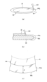
- 1A and 1B show a process for applying a metal-containing resist film to a surface of a wafer in a coating film forming method according to an embodiment, in which (a) is an oblique view, (b) is an explanatory diagram showing a schematic diagram of a portion of a side cross section, and (c) is a plan view of a portion of an edge of the wafer.
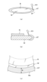
- 1A and 1B show the implementation of the first step in a coating film forming method according to an embodiment, where (a) is an oblique view, (b) is an explanatory diagram showing a schematic diagram of a portion of a side cross section, and (c) is a plan view of a portion of the edge of a wafer.
- 1A and 1B show the implementation of the second step in a coating film forming method according to an embodiment, where (a) is an oblique view, (b) is an explanatory diagram showing a schematic diagram of a portion of a side cross section, and (c) is a plan view of a portion of the edge of a wafer.
- FIG. 1A and 1B show the implementation of the third step in a coating film forming method according to an embodiment, where (a) is an oblique view, (b) is an explanatory diagram showing a schematic diagram of a portion of a side cross section, and (c) is a plan view of a portion of the edge of a wafer.
- 5 is an explanatory diagram showing a discharge angle of a processing liquid supply nozzle in a plan view with respect to a wafer in the coating film forming apparatus according to the embodiment;
- FIG. 5 is an explanatory diagram showing a discharge angle of a processing liquid supply nozzle in a side view with respect to a wafer in the coating film forming apparatus according to the embodiment.
- FIG. 13 is a plan view illustrating an arrangement of three processing liquid supply nozzles arranged on the front surface side of the wafer;
- FIG. 10 is a plan view illustrating the arrangement of rear surface nozzles arranged on the rear surface side of the wafer when the arrangement of FIG. 9 is used.
- coating films such as anti-reflective films and resist films are formed on a workpiece, such as a semiconductor wafer (hereafter referred to as "wafer") serving as a substrate.
- a workpiece such as a semiconductor wafer (hereafter referred to as "wafer") serving as a substrate.
- wafer semiconductor wafer
- a spin-coating method is often used in which a resist liquid is supplied to the wafer from above the center of the wafer and the wafer is rotated to spread the resist liquid on the wafer over the entire surface of the wafer.
- the resist solution on the wafer spreads all the way to the side edges of the wafer. Therefore, as with the technology described in Patent Document 1, the resist film formed after the application of the resist solution is removed from a certain width of area from the edge of the wafer by supplying an organic solvent such as thinner, which dissolves the resist film, to the area while rotating the wafer, thereby removing the resist film.
- metal-containing coating film (hereinafter referred to as a "metal-containing coating film") on a substrate such as a wafer in order to form finer patterns.
- FIG. 1 is an explanatory diagram showing a schematic outline of the configuration of a coating film forming apparatus 1 configured as an example of a substrate processing apparatus from the side
- FIG. 2 is an explanatory diagram showing the same schematic outline from a plan view.
- the coating film forming device 1 is equipped with a spin chuck 11, which is a substrate holding unit that holds a wafer W horizontally by vacuum-adsorbing the center of the back surface of the wafer W as a substrate, in a processing vessel 2.
- This spin chuck 11 is connected to a rotation drive mechanism 13 via a shaft 12, and is rotated around a vertical axis by the rotation drive mechanism 13.
- a circular plate 14 is provided below the spin chuck 11, surrounding the shaft portion 12 with a gap therebetween.
- Three through holes 15 are formed in the circular plate 14 in the circumferential direction, and a lift pin 16 can be inserted into each of the through holes 15.
- These lift pins 16 are supported by a lift plate 17.
- the lift plate 17 can be raised and lowered by a lift mechanism 18. By raising and lowering the lift mechanism 18, the lift pins 16 can lift the wafer W that has been released from suction from above the spin chuck 11, or place the wafer W received from a transport device (not shown) on the spin chuck 11.
- a cup body 20 is provided in the processing vessel 2 of the coating film forming apparatus 1 so as to surround the spin chuck 11.
- the cup body 20 is configured to receive waste liquid that is scattered or spilled from the rotating wafer W and to discharge the waste liquid outside the coating film forming apparatus 1.
- the cup body 20 has a mountain-shaped guide portion 21 that is arranged around the circular plate 14 and has a ring-shaped cross section, and an annular vertical wall 22 is provided so as to extend downward from the outer peripheral edge of the mountain-shaped guide portion 21.
- the mountain-shaped guide portion 21 guides liquid that has spilled from the wafer W to the outside and below the wafer W.
- the mountain-shaped guide portion 21 On the outside of the mountain-shaped guide portion 21, there is a vertical cylindrical portion 23 that surrounds the mountain-shaped guide portion 21, and an upper guide portion 24 that extends obliquely inward and upward from the upper edge of the cylindrical portion 23.
- the upper guide portion 24 is provided with a number of openings 25 in the circumferential direction.
- the upper end portion of the cylindrical portion 23 extends above the spin chuck 11, and the inner edge of the end portion is provided with an inclined body 23a that extends inward and upward.
- a ring-shaped liquid receiving portion 26 with a concave cross section is formed below the mountain-shaped guide portion 21 and the cylindrical portion 23 on the lower side of the cylindrical portion 23.
- a drainage path 27 is connected to the outer periphery of this liquid receiving portion 26.
- Two exhaust pipes 28 are provided on the inner periphery side of the drainage path 27 in the liquid receiving portion 26.
- a rail 30 is formed on the cup body 20 on the negative X-direction (downward in FIG. 2) side, extending along the Y-direction (left-right direction in FIG. 2).
- the rail 30 is positioned, for example, from the outside of the cup body 20 on the negative Y-direction (leftward in FIG. 2) side to the outside of the cup body 20 on the positive Y-direction (rightward in FIG. 2).
- a first arm 31 and a second arm 41 are provided on the rail 30 so as to be freely movable along the rail 30.
- the first arm 31 supports a resist liquid supply nozzle 32 that supplies a metal-containing resist liquid, which is a coating liquid that contains metal.
- the metal-containing resist liquid is supplied to the resist liquid supply nozzle 32 from a metal-containing resist liquid supply source 33 via a supply path 34.
- the first arm 31 is movable along the Y direction on the rail 30 by a nozzle drive unit 35. This allows the resist liquid supply nozzle 32 to move at least to above the center of the wafer W held by the spin chuck 11 within the cup body 20.
- the first arm 31 can also be raised and lowered by the nozzle drive unit 35, allowing the height of the resist liquid supply nozzle 32 to be adjusted.
- the second arm 41 supports a processing liquid supply nozzle 42 as a first processing liquid supply unit that supplies a first processing liquid, such as an organic solvent such as PEGMEA (propylene glycol monomethyl ether acetate), which dissolves and removes the coating film (e.g., zirconium oxide film) formed by the metal-containing resist liquid described above, and a processing liquid supply nozzle 43 as a second processing liquid supply unit that supplies a second processing liquid, such as an acid thinner, which is an acid processing liquid that dissolves the metal in the metal-containing coating film.
- a first processing liquid such as an organic solvent such as PEGMEA (propylene glycol monomethyl ether acetate)
- PEGMEA propylene glycol monomethyl ether acetate
- the processing liquid supply nozzle 42 also serves as a third processing liquid supply unit. That is, after supplying the second processing liquid, the processing liquid supply nozzle 42 supplies a third processing liquid, for example, PEGMEA, for cleaning the surface of the wafer W.
- the processing liquid supply nozzle 42 also serves as a first processing liquid supply unit and a third processing liquid supply unit, and in this example, the first processing liquid and the third processing liquid are the same solvent PG, PEGMEA.
- the first processing liquid and the third processing liquid, solvent PG are supplied to the processing liquid supply nozzle 42 from a supply source 44 via a supply path 45.
- the second processing liquid, acid thinner is supplied to the processing liquid supply nozzle 43 from an acid thinner supply source 46 via a supply path 47.
- the second arm 41 is movable on the rail 30 by the nozzle drive unit 48. This allows the processing liquid supply nozzles 42, 43 to move from at least the upper end of the wafer W in the cup body 20 to a certain width area.
- the nozzle drive unit 48 also allows the second arm 41 to be raised and lowered freely, allowing the height of the processing liquid supply nozzles 42, 43 to be adjusted.
- a first back surface nozzle 51 as a fifth processing liquid supply unit that supplies the above-mentioned PEGMEA and a second back surface nozzle 52 as a fourth processing liquid supply unit that supplies acid thinner are arranged on the inner periphery side of the mountain-shaped guide portion 21.
- the supply direction (discharge direction) of the liquid from the first back surface nozzle 51 and the second back surface nozzle 52 is directed obliquely outward from the underside of the periphery of the wafer W.
- the first back surface nozzle 51 is located closer to the center of the wafer W than the second back surface nozzle 52.
- the above-described coating film forming apparatus 1 is provided with at least one control unit 100 as shown in FIG. 1.
- the control unit 100 processes computer-executable instructions that cause the coating film forming apparatus 1 to execute various steps described in the present disclosure.
- the control unit 100 may be configured to control each element of the coating film forming apparatus 1 to execute various steps described herein. In one embodiment, a part or all of the control unit 100 may be included in the coating film forming apparatus 1.
- the control unit 100 may include a processing unit, a storage unit, and a communication interface.
- the control unit 100 is realized, for example, by a computer.
- the processing unit may be configured to read a program that provides logic or routines that enable various control operations to be performed from the storage unit, and to perform various control operations by executing the read program.
- This program may be stored in the storage unit in advance, or may be acquired via a medium when necessary. The acquired program is stored in the storage unit, and is read from the storage unit by the processing unit and executed.
- the medium may be various computer-readable storage media, or may be a communication line connected to the communication interface.
- the storage medium may be temporary or non-temporary.
- the processing unit may be a CPU (Central Processing Unit), or may be one or more circuits.
- the storage unit may include a RAM (Random Access Memory), a ROM (Read Only Memory), a HDD (Hard Disk Drive), a SSD (Solid State Drive), or a combination thereof.
- the communication interface may communicate with the coating film forming apparatus 1 via a communication line such as a LAN (Local Area Network).
- a metal-containing resist liquid for forming a zirconium oxide film is supplied from above the center of the wafer W held on the spin chuck 11, and the wafer W is rotated to spread the resist liquid over the entire surface of the wafer W to form a metal-containing resist film R.
- the rotation speed is, for example, 1400 rpm.
- the metal-containing resist film R is formed up to the end Wt of the side surface of the wafer W, as shown in FIG. 3(b) and (c).
- PEG-MEA is used as the solvent PG.
- the rotation speed of the wafer W in the first step is, for example, 1000 rpm.
- the processing liquid supply nozzle 42 supplies the solvent PG to an area of width A on the front surface of the wafer W
- the first rear surface nozzle 51 also supplies the solvent PG to the peripheral portion of the rear surface of the wafer W.
- the solvent PG is PEGMEA.
- a processing liquid supply nozzle 43 is moved to the vicinity of the edge of the wafer W in place of the processing liquid supply nozzle 42. Then, while rotating the wafer W, a processing liquid AT that dissolves the metal in the metal-containing resist film R is supplied to a region of a certain width B in the radial direction from the edge Wt of the wafer W as also shown in FIGS. 5(b) and 5(c). This dissolves and removes any metal components that remain in the region of width B.
- acid thinner is used as the processing liquid AT that dissolves the metal.
- the rotation speed of the wafer W in the second step is, for example, 1000 rpm.
- the processing liquid AT which is acid thinner
- the processing liquid AT is also being supplied from the second back surface nozzle 52 to the peripheral portion of the back surface of the wafer W.
- ⁇ Third step> 6(a) the processing liquid supply nozzle 42 moves again to the vicinity of the edge of the wafer W, instead of the processing liquid supply nozzle 43. Then, while rotating the wafer W, as shown in FIGS. 6(b) and 6(c), a solvent PG of the metal-containing resist liquid is supplied to an area of a certain width C in the radial direction from the edge Wt of the wafer W. This washes away the acid thinner remaining in the area of width C.
- the solvent PG is the PEG-MEA described above.
- the rotation speed of the wafer W in the third step is, for example, 1000 rpm.
- the processing liquid supply nozzle 42 supplies the solvent PG to an area of width C on the surface of the wafer W
- the first back surface nozzle 51 also supplies the solvent PG to the peripheral portion of the back surface of the wafer W.
- the relationship between the lengths of width A, width B, and width C is A>C>B.
- the metal-containing resist film R formed on the surface of the wafer W is removed in a circular shape from the edge Wt of the wafer W in a region of width A in the radial direction by the solvent PG.
- the surface of the wafer W in a region of width B narrower than width A is cleaned with acid thinner, and any metal components remaining in the region of width B are dissolved and removed.
- the surface of the wafer W in a region of width C wider than width B and narrower than width A is cleaned with solvent PG, and the acid thinner remaining in the region of width C is washed away.
- the peripheral portion of the metal-containing resist film R can be effectively removed, and the occurrence of defects in the metal-containing coating and the underlying film on the substrate surface can be suppressed when removing the peripheral portion of the metal-containing coating.
- width A, width B, and width C are A>C>B for the following reason. That is, in the first step, when the region of width A in the metal-containing resist film R is dissolved and removed by the solvent PG, metal components in the dissolved film components may remain on the surface of the wafer W after the film has been removed. If this is left as it is, as already mentioned, it may adversely affect subsequent processes or become a cause of cross-contamination.
- a processing liquid AT for dissolving the metal components is supplied to the surface of the wafer W after the film has been removed, for example, an acid thinner, which is a mixture of an acidic agent and a thinner.
- a solvent PG is supplied to wash away the processing liquid AT.
- the width C of the area where the solvent PG is supplied in the third step is larger than the width B of the area where the processing liquid AT is supplied in the second step in order to completely wash away the processing liquid AT supplied in the second step.
- the width C of the area where the solvent PG is supplied in the third step is smaller than the width A of the area where the solvent PG is supplied in the first step in order to prevent the washed-out processing liquid AT from penetrating through the interface of the metal-containing resist film R and to prevent the metal components in the metal-containing resist film R from flowing out.
- the discharge angle of the processing liquid supply nozzles 42, 43 shown in FIG. 7 relative to the wafer W in plan view i.e., the angle ⁇ 1 relative to the tangent line of the wafer W
- the processing liquid supply nozzle 42 that supplies the solvent PG it is set to, for example, 8.5 degrees.
- ⁇ 1 is set to, for example, 30 degrees.
- the processing liquid supply nozzle 43 that supplies the processing liquid AT is directed radially outward more than the processing liquid supply nozzle 42 that supplies the solvent PG. This is to prevent the supplied processing liquid AT from splashing or scattering inward, and also to allow the solvent PG to spread further inward when the processing liquid AT is subsequently washed away with the solvent PG.
- the discharge angle of the processing liquid supply nozzles 42, 43 with respect to the wafer W in a side view i.e., the depression angle ⁇ 2 is set to, for example, 45 degrees for both processing liquid supply nozzles 42, 43.
- the processing liquid supply nozzle 43 that supplies the processing liquid AT is directed further outward than the processing liquid supply nozzle 42 that supplies the solvent PG, so that the processing liquid AT supplied from the processing liquid supply nozzle 43 is prevented from moving toward the center of the wafer W, and the processing liquid AT supplied in the subsequent third step can be thoroughly cleaned by the solvent PG.
- the solvent PG used in the first step and the solvent PG used in the third step are the same solvent, but since the purpose of the solvent supplied in the third step is to wash away the processing liquid AT supplied in the second step, the liquid supplied in the third step may be another solvent. For example, it may be pure water.
- the nozzle for supplying the processing liquid can use the common processing liquid supply nozzle 42.
- the liquid supplied in the third step is a liquid different from the solvent PG used in the first step, such as pure water, it is necessary to use different nozzles for each supply. In other words, the supply nozzles as the first processing liquid supply unit, the second processing liquid supply unit, and the third processing liquid supply unit must be separate.
- the rotation speed of the wafer W in the first, second, and third steps was set to 1000 rpm, but the rotation speed in the second step in which the processing liquid AT is supplied may be faster than the rotation speed in the first and third steps in which the solvent PG is supplied. This is to prevent droplets from scattering toward the area where the solvent PG is supplied when the processing liquid AT is supplied.
- the solvent PG is also supplied from the first back nozzle 51 on the back side of the wafer W
- the processing liquid AT is also supplied from the second back nozzle 52.
- the liquid supplied from each of these back nozzles is the same liquid as the liquid supplied from the front side of the wafer W.
- the purpose is to prevent the liquid supplied to the front side of the wafer W from flowing around to the back side of the wafer W. Therefore, the positions of the first back nozzle 51 and the second back nozzle 52 arranged on the back side do not need to be set as strictly as the processing liquid supply nozzles 42, 43 arranged on the front side of the wafer W.
- the first rear nozzle 51 and the second rear nozzle 52 arranged on the rear side are positioned opposite the processing liquid supply nozzles 42, 43 arranged on the front side of the wafer W, sandwiching the wafer W therebetween.
- the radial positions of the first rear nozzle 51 and the second rear nozzle 52 arranged on the rear side are located more inward than the processing liquid supply nozzles 42, 43 arranged on the front side of the wafer W, i.e., closer to the center of the wafer W.
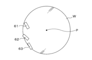
- FIG. 9 is a schematic plan view of the arrangement of the first, second, and third processing liquid supply nozzles, which are separate units arranged on the front side of the wafer W as processing liquid supply nozzles 61, 62, and 63.
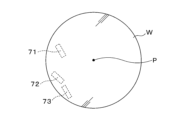
- FIG. 10 is a schematic plan view of the arrangement of rear nozzles 71, 72, and 73 arranged on the rear side in this case.
- the front side processing liquid supply nozzles 61, 62, and 63 are omitted from FIG. 10.
- the rear nozzles 71, 72, 73 arranged on the rear side are positioned opposite the processing liquid supply nozzles 61, 62, 63 arranged on the front side across the wafer W, but the radial positions of the rear nozzles 71, 72, 73 are set closer to the center P of the wafer W than the processing liquid supply nozzles 61, 62, 63 arranged on the front side. This makes it possible to more reliably prevent the liquid supplied to the front side of the wafer W from the processing liquid supply nozzles 61, 62, 63 from flowing around to the rear side of the wafer W.
- the substrate processing is tentatively completed with the first step ⁇ second step ⁇ third step, but this is not limiting.
- the second step ⁇ third step may be executed again to complete the processing.
- the second step and the third step may be repeatedly performed. In this way, appropriate processing can be performed according to the remaining state of the processing liquid AT, such as metal components and acid thinner, remaining on the substrate surface.
- the coating film forming apparatus 1 described above is configured to perform the process of forming the metal-containing resist film R on the wafer W and the first, second, and third steps of removing the peripheral portion of the metal-containing resist film R within the same apparatus, but this is not limited thereto, and the process of forming the metal-containing resist film R and the first to third steps may be performed within separate apparatus or modules.
- a substrate processing apparatus for processing a substrate comprising: a substrate holder that holds and rotates a substrate on which a metal-containing coating film is formed; a first processing liquid supply unit that supplies a first processing liquid to a surface of the substrate; a second processing liquid supply unit that supplies a second processing liquid to the surface of the substrate; a third processing liquid supply unit that supplies a third processing liquid to the surface of the substrate; A control unit, The control unit is a first step of supplying the first processing liquid from the first processing liquid supply unit to a first width region from an end portion of the substrate while rotating the substrate, thereby removing the coating film; a second step of removing the metal remaining in a second width region from an end of the substrate, the second processing liquid being supplied from the second processing liquid supply unit while rotating the substrate, the second processing liquid being supplied to a second width region narrower than the first width region from an end of the substrate after the first step; a third step of, after the second step,
- the first treatment liquid is an organic solvent
- the substrate processing apparatus according to (1), wherein the third processing liquid is pure water.
- a coating liquid supply unit that supplies a metal-containing coating liquid to the substrate held by the substrate holding unit, The substrate processing apparatus described in (6), wherein the control unit is configured to execute a step of supplying the coating liquid from the coating liquid supply unit to a surface of the substrate held by the substrate holding unit before the first step, and forming the coating film.
- a fourth processing liquid supply unit that supplies a second processing liquid to the back surface of the substrate, The substrate processing apparatus according to (7), wherein, when the second processing liquid is being supplied from the second processing liquid supply unit in the second step, the fourth processing liquid supply unit supplies the second processing liquid.
- a fifth processing liquid supply unit that supplies a third processing liquid to the rear surface of the substrate, The substrate processing apparatus according to (9), wherein, when the third processing liquid is being supplied from the third processing liquid supply unit in the third step, the fifth processing liquid supply unit supplies the third processing liquid.
- the substrate processing apparatus according to (1) wherein the rotation speed of the substrate in the second step is faster than the rotation speed of the substrate in the first step and the third step.
- (12) A substrate processing apparatus as described in (1), wherein the discharge angle with respect to the tangent of the substrate in a planar view when the second processing liquid is supplied from a nozzle as the second processing liquid supply unit is directed radially outwardly relative to the discharge angle when the first processing liquid is supplied from a nozzle as the first processing liquid supply unit.
- a substrate processing method for processing a substrate comprising the steps of: a first step of supplying a first processing liquid to a first width region from an end portion of the substrate while rotating the substrate, thereby removing a coating film in the first width region; a second step of supplying a second processing liquid to a second width region narrower than the first width region from an end of the substrate while rotating the substrate, after the first step, to remove metal components remaining in the second width region; a third step of, after the second step, supplying a third processing liquid to a third width region from an end of the substrate which is narrower than the first width region and wider than the second width region while rotating the substrate, thereby washing away the second processing liquid remaining in the third width region.
Landscapes
- Physics & Mathematics (AREA)
- General Physics & Mathematics (AREA)
- Cleaning Or Drying Semiconductors (AREA)
- Exposure Of Semiconductors, Excluding Electron Or Ion Beam Exposure (AREA)
- Weting (AREA)
Priority Applications (3)
| Application Number | Priority Date | Filing Date | Title |
|---|---|---|---|
| KR1020257036295A KR20250170639A (ko) | 2023-03-30 | 2024-03-19 | 기판 처리 장치 및 기판 처리 방법 |
| JP2025510575A JPWO2024203602A1 (https=) | 2023-03-30 | 2024-03-19 | |
| CN202480020816.2A CN120917542A (zh) | 2023-03-30 | 2024-03-19 | 基片处理装置和基片处理方法 |
Applications Claiming Priority (2)
| Application Number | Priority Date | Filing Date | Title |
|---|---|---|---|
| JP2023055445 | 2023-03-30 | ||
| JP2023-055445 | 2023-03-30 |
Publications (1)
| Publication Number | Publication Date |
|---|---|
| WO2024203602A1 true WO2024203602A1 (ja) | 2024-10-03 |
Family
ID=92906148
Family Applications (1)
| Application Number | Title | Priority Date | Filing Date |
|---|---|---|---|
| PCT/JP2024/010712 Ceased WO2024203602A1 (ja) | 2023-03-30 | 2024-03-19 | 基板処理装置及び基板処理方法 |
Country Status (5)
| Country | Link |
|---|---|
| JP (1) | JPWO2024203602A1 (https=) |
| KR (1) | KR20250170639A (https=) |
| CN (1) | CN120917542A (https=) |
| TW (1) | TW202443643A (https=) |
| WO (1) | WO2024203602A1 (https=) |
Citations (5)
| Publication number | Priority date | Publication date | Assignee | Title |
|---|---|---|---|---|
| JP2017098367A (ja) * | 2015-11-20 | 2017-06-01 | 東京エレクトロン株式会社 | 基板処理方法 |
| JP2019054252A (ja) * | 2018-10-24 | 2019-04-04 | 東京エレクトロン株式会社 | 基板処理装置、基板処理方法及び記憶媒体 |
| JP2019532489A (ja) * | 2016-08-12 | 2019-11-07 | インプリア・コーポレイションInpria Corporation | 金属含有レジストからのエッジビード領域における金属残留物を低減する方法 |
| JP2020013823A (ja) * | 2018-07-13 | 2020-01-23 | 株式会社Screenホールディングス | 基板処理装置および基板処理方法 |
| JP2023041310A (ja) * | 2021-09-13 | 2023-03-24 | 株式会社Screenホールディングス | 基板処理方法 |
Family Cites Families (1)
| Publication number | Priority date | Publication date | Assignee | Title |
|---|---|---|---|---|
| JP7024307B2 (ja) | 2017-01-26 | 2022-02-24 | 東京エレクトロン株式会社 | 塗布膜除去装置、塗布膜除去方法及び記憶媒体 |
-
2024
- 2024-03-18 TW TW113109940A patent/TW202443643A/zh unknown
- 2024-03-19 KR KR1020257036295A patent/KR20250170639A/ko active Pending
- 2024-03-19 CN CN202480020816.2A patent/CN120917542A/zh active Pending
- 2024-03-19 JP JP2025510575A patent/JPWO2024203602A1/ja active Pending
- 2024-03-19 WO PCT/JP2024/010712 patent/WO2024203602A1/ja not_active Ceased
Patent Citations (5)
| Publication number | Priority date | Publication date | Assignee | Title |
|---|---|---|---|---|
| JP2017098367A (ja) * | 2015-11-20 | 2017-06-01 | 東京エレクトロン株式会社 | 基板処理方法 |
| JP2019532489A (ja) * | 2016-08-12 | 2019-11-07 | インプリア・コーポレイションInpria Corporation | 金属含有レジストからのエッジビード領域における金属残留物を低減する方法 |
| JP2020013823A (ja) * | 2018-07-13 | 2020-01-23 | 株式会社Screenホールディングス | 基板処理装置および基板処理方法 |
| JP2019054252A (ja) * | 2018-10-24 | 2019-04-04 | 東京エレクトロン株式会社 | 基板処理装置、基板処理方法及び記憶媒体 |
| JP2023041310A (ja) * | 2021-09-13 | 2023-03-24 | 株式会社Screenホールディングス | 基板処理方法 |
Also Published As
| Publication number | Publication date |
|---|---|
| KR20250170639A (ko) | 2025-12-05 |
| CN120917542A (zh) | 2025-11-07 |
| JPWO2024203602A1 (https=) | 2024-10-03 |
| TW202443643A (zh) | 2024-11-01 |
Similar Documents
| Publication | Publication Date | Title |
|---|---|---|
| JP6314779B2 (ja) | 液処理方法、記憶媒体及び液処理装置 | |
| US9805958B2 (en) | Substrate cleaning apparatus, substrate cleaning method and non-transitory storage medium | |
| JP7073658B2 (ja) | 基板処理方法、基板処理装置、及び記憶媒体 | |
| JP6102807B2 (ja) | 基板洗浄装置、基板洗浄方法及び記憶媒体 | |
| JP7535933B2 (ja) | 現像方法及び基板処理システム | |
| KR102714523B1 (ko) | 기판 처리 방법, 기억 매체 및 현상 장치 | |
| JP7490503B2 (ja) | 基板処理方法および基板処理装置 | |
| KR101950047B1 (ko) | 기판 세정 건조 방법 및 기판 현상 방법 | |
| TW201629641A (zh) | 顯影方法 | |
| TWI849104B (zh) | 基板處理方法及基板處理裝置 | |
| WO2024203602A1 (ja) | 基板処理装置及び基板処理方法 | |
| JP7329418B2 (ja) | 基板処理方法及び基板処理装置 | |
| TW201802875A (zh) | 顯影方法、顯影裝置及記錄媒體 | |
| JP7202960B2 (ja) | 塗布膜形成方法及び塗布膜形成装置 | |
| WO2026038499A1 (ja) | 基板処理装置及び基板処理方法 | |
| WO2025079441A1 (ja) | 基板処理方法及び基板処理装置 | |
| US20250239469A1 (en) | Protective film forming method, protective film forming apparatus, and substrate treatment system | |
| JP2025112257A (ja) | 保護膜形成方法、保護膜形成装置及び基板処理システム | |
| WO2024241937A1 (ja) | 現像方法及び基板処理システム | |
| CN113391528A (zh) | 改善光阻显影均匀性的方法 |
Legal Events
| Date | Code | Title | Description |
|---|---|---|---|
| 121 | Ep: the epo has been informed by wipo that ep was designated in this application |
Ref document number: 24779727 Country of ref document: EP Kind code of ref document: A1 |
|
| ENP | Entry into the national phase |
Ref document number: 2025510575 Country of ref document: JP Kind code of ref document: A |
|
| WWE | Wipo information: entry into national phase |
Ref document number: 2025510575 Country of ref document: JP |
|
| WWE | Wipo information: entry into national phase |
Ref document number: 202480020816.2 Country of ref document: CN |
|
| ENP | Entry into the national phase |
Ref document number: 1020257036295 Country of ref document: KR Free format text: ST27 STATUS EVENT CODE: A-0-1-A10-A15-NAP-PA0105 (AS PROVIDED BY THE NATIONAL OFFICE) |
|
| WWE | Wipo information: entry into national phase |
Ref document number: KR1020257036295 Country of ref document: KR |
|
| NENP | Non-entry into the national phase |
Ref country code: DE |
|
| WWP | Wipo information: published in national office |
Ref document number: 202480020816.2 Country of ref document: CN |
|
| 122 | Ep: pct application non-entry in european phase |
Ref document number: 24779727 Country of ref document: EP Kind code of ref document: A1 |