WO2024201700A1 - 測定装置 - Google Patents
測定装置 Download PDFInfo
- Publication number
- WO2024201700A1 WO2024201700A1 PCT/JP2023/012443 JP2023012443W WO2024201700A1 WO 2024201700 A1 WO2024201700 A1 WO 2024201700A1 JP 2023012443 W JP2023012443 W JP 2023012443W WO 2024201700 A1 WO2024201700 A1 WO 2024201700A1
- Authority
- WO
- WIPO (PCT)
- Prior art keywords
- probes
- component
- measuring
- measuring device
- contact
- Prior art date
- Legal status (The legal status is an assumption and is not a legal conclusion. Google has not performed a legal analysis and makes no representation as to the accuracy of the status listed.)
- Ceased
Links
Images





Classifications
-
- G—PHYSICS
- G01—MEASURING; TESTING
- G01R—MEASURING ELECTRIC VARIABLES; MEASURING MAGNETIC VARIABLES
- G01R31/00—Arrangements for testing electric properties; Arrangements for locating electric faults; Arrangements for electrical testing characterised by what is being tested not provided for elsewhere
- G01R31/26—Testing of individual semiconductor devices
-
- G—PHYSICS
- G01—MEASURING; TESTING
- G01R—MEASURING ELECTRIC VARIABLES; MEASURING MAGNETIC VARIABLES
- G01R31/00—Arrangements for testing electric properties; Arrangements for locating electric faults; Arrangements for electrical testing characterised by what is being tested not provided for elsewhere
- G01R31/28—Testing of electronic circuits, e.g. by signal tracer
Definitions
- This disclosure relates to a measuring device that measures electrical characteristics of components.
- Patent Document 1 describes a measuring device in which a pair of probes are arranged side by side, and the electrode parts on both sides of a component are brought into contact with the respective probes to measure the electrical characteristics of the component.
- the pair of probes are arranged so that they can rotate about the parts opposite to the sides that face each other, and the parts that face each other are provided with an upward elastic force by a spring member. Therefore, even if the heights of the electrode parts on both sides of the component vary from left to right or the component is picked up at an angle to the suction nozzle [0054], the electrode parts on both sides of the component can be brought into contact with the respective probes to measure the electrical characteristics of the component.
- the objective of this disclosure is to improve a measuring device that measures the electrical characteristics of components, for example, by making it possible to measure the electrical characteristics of components effectively.
- the contact portions of the multiple probes come into contact with the electrode portions on both sides of the component to measure the electrical characteristics of the component. Furthermore, the multiple contact portions of the multiple probes form a generally V-shaped recess. In the generally V-shaped recess, the spacing between the opposing contact portions is narrow in the center and wide in the periphery. Therefore, even if each of the multiple probes is not rotatable as described in Patent Document 1, the electrode portions on both sides of the component can be brought into good contact with the multiple probes, and the electrical characteristics of the component can be well measured.
- FIG. 1 is a perspective view of a mounting machine including a measurement device according to an embodiment of the present disclosure.
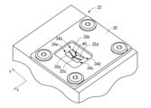
- FIG. 1 is a perspective view conceptually illustrating a measurement device according to a first embodiment of the present disclosure.
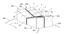
- FIG. 2 is a perspective view conceptually showing the main portion and components of the measuring device.
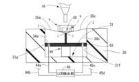
- FIG. 2 is a front view conceptually showing the measuring device.
- FIG. 2 is a diagram showing an electrical characteristic measuring circuit of the measuring device.
- FIG. 2 is a diagram showing a coaxial cable of the measuring device.
- FIG. 2 is a diagram showing the periphery of a control device of the placement machine.
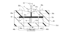
- FIG. 4 is a front view conceptually showing another aspect of the main part of the measuring device.
- FIG. 1 is a perspective view conceptually illustrating a measurement device according to a first embodiment of the present disclosure.
- FIG. 2 is a perspective view conceptually showing the main portion and components of the measuring device.
- FIG. 2 is a front view conceptually showing the measuring device.
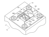
- FIG. 11 is a perspective view conceptually illustrating a measurement device according to a second embodiment of the present disclosure.
- FIG. 2 is a perspective view conceptually showing a main part of the measuring device.
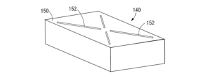
- FIG. 2 is a perspective view conceptually showing a holding portion of the measuring device.
- 2 is a front view (partially sectional view) conceptually showing a state in which electrical characteristics of a component are measured by the measuring device.
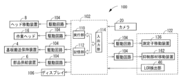
- FIG. FIG. 2 is a diagram showing the periphery of a control device of the placement machine.
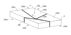
- FIG. 2 is a perspective view conceptually showing another aspect of the main part of the measuring device.
- the measuring device can be called an electrical characteristic acquisition device.
- the mounting machine shown in FIG. 1 mounts electronic components (hereinafter simply referred to as components) s onto a circuit board, and includes a main body 2, a circuit board conveying and holding device 4, a component supplying device 6, a head moving device 8, and the like.
- the circuit board transport and holding device 4 transports and holds the circuit board P (hereinafter, abbreviated as board P) in a horizontal position, and in FIG. 1, the transport direction of the board P is the x direction, the width direction of the board P is the y direction, and the thickness direction of the board P is the z direction.
- the y direction and the z direction are the front-to-back and up-to-down directions of the mounting machine, respectively.
- the component supply device 6 supplies components (e.g., elements) s to be mounted on the board P, and includes a plurality of tape feeders 14, etc.
- the head moving device 8 holds the working head 16 and moves it in the x, y, and z directions.
- the working head 16 includes a component holder 18 that holds the components s, etc.
- the reference numeral 20 denotes a camera.
- the camera 20 captures an image of the component s held by the suction nozzle 18, and based on the image captured by the camera 20, it is determined whether or not the component s is to be mounted on the circuit board P.
- the reference numeral 22 denotes a measuring device.
- the measuring device 22 measures the electrical characteristics of the component s, and is held by the substrate transport and holding device 4 via the storage section 26.
- the electrical characteristics of the component s include L (inductance), C (capacitance), R (resistance), X (reactance), Z' (impedance), etc., and the measuring device 22 measures one or more of these.
- the component s whose electrical characteristics are measured by the measuring device 22, is a square chip having a functional part r provided in the middle and electrode parts t provided at both ends, as shown in Figure 3 etc.
- the functional part r is covered on the outside with an insulating material.
- the measuring device 22 includes a main body 30 and one or more measuring units 32 provided on the main body 30.
- the measuring unit 32 includes four measuring elements 34a, 34b, 34c, and 34d as a plurality of measuring elements (which can be referred to as measuring terminals), a measuring element moving device 36 for moving the four measuring elements 34a, 34b, 34c, and 34d as a unit, and the like.
- a recess 31 is provided on the main body 30, and the four measuring elements 34a, 34b, 34c, and 34d, the measuring element moving device 36, and the like are provided in the recess 31.
- the probes 34a, 34b, 34c, and 34d are collectively referred to or described without distinction, they will be simply referred to as the probe 34. The same applies to the contact portion, the coaxial cable, and the like.
- Each of the four probes 34 is generally rectangular, with its upper surface serving as a contact portion 35 (35a, 35b, 35c, 35d) that comes into contact with the part s.
- the upper surface of the contact portion 35 is generally rectangular, with a first side i, one of the sides that make up the rectangle, positioned lower than a second side j that faces the first side i, and is inclined in one direction.
- the upper surface can be referred to as a contact surface.
- a generally V-shaped recess 40 is formed by the contact portions 35a, 35b of the probes 34a, 34b and the contact portions 35c, 35d of the probes 34c, 34d. This V-shaped recess 40 functions as a component placement portion 40 on which the component s is placed.
- an insulator portion 42 made of an insulating material is interposed between each of the four probes 34. Since the four probes 34 are arranged in two rows and two columns, the insulator portions 42 are arranged generally in a cross shape.
- the insulator portion 42 may be a gas such as air or a solid material such as glass. However, if it is a solid material, the spacing between the probes 34 can be narrowed, making it possible to measure the electrical characteristics of smaller components s.
- two of the four probes 34, 34a and 34b are connected to coaxial cables 44a and 44b, respectively, and the two probes 34c and 34d are connected to coaxial cables 45c and 45d, respectively.
- the coaxial cables 44 and 45 are connected to an LCR detector 46, and an electrical characteristic measuring circuit 49 is formed by these coaxial cables 44 and 45, the four probes 34, the LCR detector 46, etc.
- the coaxial cables 44a, 44b, 45c, and 45d described above each have the same structure, and as shown in FIG. 6, each include an inner conductor 50, an insulator (dielectric) 52, an outer conductor 54, and a protective coating 56, which are arranged coaxially.
- the provision of the outer conductor 54 prevents the transmitted signal from leaking to the outside.
- One end of each of the coaxial cables 44a, 44b, 45c, and 45d (one end of the inner conductor 50) is connected to the probes 34a, 34b, 34c, and 34d, respectively, and the other end is connected to the LCR detector 46.
- the coaxial cables 44 and 45 are connected by a four-terminal pair connection method, and the electrical characteristics of the component s are measured by the automatic balancing bridge method.
- the other end of the coaxial cable 44b is connected to the Hc terminal and is connected to an AC power source.
- the output of the AC power source is supplied to the inner conductor 50 of the coaxial cable 44b and returned via the outer conductor 54.
- the other end of the coaxial cable 44a is connected to the Hp terminal and is connected to a voltage sensor.
- the potential difference between the inner conductor 50 and the outer conductor 54 is detected as a voltage value applied to the component s.
- the other end of the coaxial cable 45d is connected to the Lc terminal and then to a current sensor.
- the current flowing between the inner conductor 50 and the outer conductor 54 is obtained as the current value flowing through the component s.
- the potential difference of a resistor (not shown) provided between the inner conductor 50 and the outer conductor 54 is obtained, and the current flowing through the resistor is obtained based on the potential difference and the resistance value Rx of the resistor.
- the other end of the coaxial cable 45c is connected to the Lp terminal.
- the potential difference between the inner conductor 50 and the outer conductor 54 is detected, and the components (oscillator, etc.) of the LCR detection unit 46 (not shown) are controlled so that the detected potential difference becomes zero.
- the current flowing through the resistor and the current flowing through the component s become the same, and the current flowing through the resistor obtained at the terminal Lc in this state becomes the current value flowing through the component s.
- 60 indicates an identical potential portion.
- the outer conductors 54 of the coaxial cable portions 44 and 45 are at the same ground potential, making it possible to reduce noise and stably measure the electrical characteristics of the component s.
- the current flowing through the component s and the voltage applied to the component s are measured by separate circuits, and the currents flowing through the internal conductor 50 and the external conductor 54 are made to flow in opposite directions. This makes it possible to suppress the generation of magnetic flux in each of the internal conductor 50 and the external conductor 54, and allows the current and voltage flowing through the component s to be measured with high accuracy.
- the method of connecting the coaxial cable and the method of measuring the electrical characteristics of the component s are not important.
- the probe moving device 36 moves the four probes 34 as a whole in the vertical direction (z direction) relative to the main body 30.
- the probe moving device 36 can include a drive source such as an electric motor, a solenoid, or a fluid pressure cylinder.
- the four probes 34 are arranged in two rows and two columns and held by a holding plate 62.
- the holding plate 62 is moved vertically by the probe moving device 36, whereby the four probes 34 are moved vertically as a unit.
- the opposing side surfaces 31f, 31g extending in the vertical direction of the recess 31 of the main body 30 function as a guide for at least one of the holding plate 62 and the probes 34.
- the holding plate 62 may be made of an insulating material.
- the placement machine includes a control device 100.
- the control device 100 includes a controller 102, which is mainly a computer, and multiple drive circuits 104.
- the controller 102 includes an execution unit 110, a memory unit 112, an input/output unit 114, etc., to which the board transport and holding device 4, the component supply device 6, the head moving device 8, the work head 16, the probe moving device 36 of the measuring device 22, etc. are each connected via the drive circuits 104, as well as to an LCR detection unit 46, a display 106, a camera 20, etc. These are controlled by the execution of multiple programs, such as an LCR measurement program (not shown) stored in the memory unit 112.
- an LCR measurement program not shown
- the placement machine including the measuring device 22 configured as above will be described. For example, when a command to measure the electrical characteristics of component s is issued, such as when a new tape feeder 14 is set or when a tape feeder 14 is replaced, the electrical characteristics of component s held by that tape feeder 14 are measured.
- the component s is held by the component holder 18 of the work head 16, transported from the component supply device 6 to the measuring device 22, released from the component holder 18, and placed on the component placement section 40.
- the (pair of) electrode portions t on both sides of the component s are considered to be in contact with the contact portions 35 of the four probes 34.
- each of a pair of bottom portions (bottom portions of a pair of electrode portions t) constituting the bottom surface of the component s is considered to be in line contact with the contact portions 35 of two probes 34.
- the electrical characteristics of the component s can be obtained by the four-terminal contact method.
- the component s and the contact portions 35 are in line contact, it is possible to prevent dirt from adhering to the contact portions 35, thereby improving the measurement accuracy of the electrical characteristics.
- the four contact portions 35 form a generally V-shaped recess, making it easier for the pair of electrode portions t to come into contact with the contact portions 35 of the four probes 34. This makes it possible to satisfactorily measure the electrical characteristics of the component s.
- the electrical characteristics can be measured even if the size of the component s is different.
- the contact portion 35 forms a generally V-shaped recess, and the bottom edge of each of the pair of electrode portions t of the component s is in line contact with the contact portion 35, the contact pressure between the component s and the contact portion 35 can be increased compared to when the bottom surface of each of the pair of electrode portions t of the component s is in surface contact with the contact portion 35, making it possible to measure electrical characteristics more accurately.
- the electrical characteristics of the component s can be measured while the component s is held by the component holder 18. In that case, the component holder 18 presses the component s against the contact parts 35 of the four probes 34, so that the pair of electrode parts t of the component s can be brought into better contact with the contact parts 35 of the four probes 34.
- the four probes 34 can be moved upward by the probe moving device 36. Even when the four probes 34 are moved upward, the upward movement of the component s is suppressed by the component holder 18. As a result, it becomes possible to press the contact portions 35 of the four probes 34 against the pair of electrode portions t of the component s, and the contact portions 35 of the four probes 34 can be brought into better contact with the pair of electrode portions t of the component s.
- the probe moving device 36 is not essential. Instead, the probe moving device 36 can be configured to move each of the four probes 34 separately and independently in the vertical direction.
- an elastic member can be provided instead of the probe moving device 36.
- the four probes 34 are held in the center of the holding plate 70. Therefore, the peripheral portion 70r of the holding plate 70 is located outside the four probes 34.
- One or more spring members 72 serving as elastic members are provided between the lower surface of the holding plate 70 and the bottom surface 31b of the recess 31 of the main body 30. The spring members 72 apply an elastic force in the vertical direction to the four probes 34.
- the recess 31 of the main body 30 generally has a stepped shape and includes a wide recess 31a on the bottom side and a narrow recess 31c on the opening side.
- the bottom surface 31b is the bottom surface of the wide recess 31a.
- the retaining plate 70 is located in the wide recess 31a, and functions as a stopper by the step surface 31d between the wide recess 31a and the narrow recess 31c abutting against the upper surface of the peripheral portion 70r of the retaining plate 70. In the normal state (non-measurement state), the upper surface of the peripheral portion 70r of the retaining plate 70 is in abutment against the step surface 31d of the main body 30.
- the component holder 18 presses the component s against the four probes 34.
- the component holder 18 elastically deforms the spring member 72 and moves the four probes 34 downward.
- the spring member 72 applies an upward force to the four probes 34.
- the four probes 34 are pressed firmly against a pair of electrode portions t of the component s held by the component holder 18, and the contact portions 35 make good contact with the electrode portions t of the component s.
- four probes 34 are provided, but two probes 34 may be provided. In that case, the two probes 34 are connected to the LCR detection unit by the two-terminal method.
- the measuring section 132 of the measuring device 122 includes four measuring probes 134 (134a, 134b, 134c, 134d), a measuring probe moving device 136 (see Figure 13), a movement suppression device 138, a holding table 140 as a holding section, etc.
- Each of the four probes 134 is generally blade-shaped as a plate, and the upper edge of the blade-shaped probe 134 is the contact portion 135.
- the contact portion 135 is inclined in one direction, in other words, in such a direction that the first end m is located lower than the second end n.
- Each of the four probes 134 is generally trapezoidal or triangular in side view.
- the four probes 134 are radially arranged with the first end m as the center, in other words, with the first ends m facing each other and each plate surface extending substantially vertically.
- the four probes 134 are positioned roughly in an X-shape when viewed from above.
- a roughly conical or pyramidal recess 143 is formed by the four contact portions 135.
- An insulator portion 142 is provided between the four probes 134, in other words, in the central portion of the four probes 134 (in the vicinity of the first end m of each of the four probes 134).
- coaxial cables 144, 145 are connected to each of the four probes 134, respectively, and are connected using the four-terminal pair connection method, as in Example 1.
- the sensor head moving device 136 moves the four sensor heads 134 vertically, either together or separately.
- the sensor head moving device 136 can include a driving source such as an electric motor, a solenoid, or a fluid pressure cylinder.
- the holding table 140 holds the component s. Because the four probes 134 are blade-shaped, it may be difficult to stably hold the component s (the component before its electrical characteristics are measured) which is the object whose electrical characteristics are to be measured. Therefore, in this embodiment, the component s which is the object whose electrical characteristics are to be measured is placed on the holding table 140.
- the holding table 140 is generally cylindrical (box-shaped) with a bottom, and is disposed with the bottom facing up.
- the four probes 134 are located in the space inside the cylindrical portion (side portion) of the holding table 140.
- the upper surface of the bottom portion of the holding table 140 is made into a component placement portion 150.
- the component placement portion 150 is formed with four holding table through holes 152, which are through holes corresponding to the four probes 134, respectively.
- Each of the four holding table through holes 152 is an elongated hole (slit) extending in one direction.
- Each of the four holding table through holes 152 has a width larger than the width (thickness) of each of the four probes 134, a length longer than the length of the four probes 134, and is provided generally in an X shape. Therefore, when the four probes 134 are moved upward by the probe moving device 136, they can protrude above the component mounting portion 150 through the holder through-holes 152. The four probes 134 protrude from the second end n.
- the movement suppression device 138 includes a movement suppression member 160 and a suppression member moving device 162 that moves the movement suppression member 160 between an active position above the component s and a retracted position away from the position above the component s.
- the movement suppression member 160 is a generally plate-shaped member in which four suppression member through holes 164 that extend radially (in an X-shape) are formed. Each of the suppression member through holes 164 is an elongated hole that extends in one direction and is provided to correspond to the four measuring probes 134.
- the suppression member moving device 162 moves the movement suppression member 160 along a pair of guides 166a, 166b.
- the suppression member moving device 162 can include a driving source such as an electric motor, a solenoid, or a fluid pressure cylinder.
- the component s is placed on the component placement section 150 of the holding table 140, and the movement suppression member 160 is moved to the operating position.
- the movement suppression member 160 is positioned on the opposite side of the four measuring probes 134 of the component s. In other words, the movement suppression member 160 is positioned above the component placement section 150 (component s), and the four measuring probes 134 are positioned below the component placement section 150.
- the four probes 134 are moved upward.
- Each of the four probes 134 passes through the holder through-hole 152, protrudes upward from the component mounting surface 150, and comes into contact with the component s.
- the component s is moved upward and comes into contact with the movement suppressing member 160.
- the contact portions 135 of the four probes 134 are pressed against a pair of electrode portions t of the component s, and the contact portions 135 come into good contact with the electrode portions t of the component s.
- a portion (near the second end n) of the four probes 134 may pass through the suppression member through-hole 164 and protrude upward.
- the four probes 134 may pierce the electrode portion t of the component s.
- the contact portions 135 of the four probes 134 are the edges of the blade-shaped members, they are less susceptible to oxidation and are less susceptible to adhesion of dirt.
- the suppression member moving device 162 moves the movement suppression member 160 linearly between the retracted position and the operating position, but the suppression member moving device 162 may rotate the movement suppression member 160 between the retracted position and the operating position.
- the movement suppression member 160 is not essential.
- the component s can also be held from above by the component holder 18 of the work head 16.
- each of the four probes 234 may be formed and arranged in the shape shown in FIG.
- Each of the four probes 234 is generally rectangular parallelepiped-shaped, with the contact portion 235, which is the upper surface, tilted in one direction with a first corner p, one of the four corners, located lower than a second corner q, which is the corner diagonally opposite the first corner p.
- the four probes 234 are arranged in two rows and two columns with the first corner p at the center via the insulator portion 242.
- the four contact portions 235 form a generally pyramidal recess 250.
- the pyramidal recess 250 functions as a component mounting portion.
- the measuring device 22, 122 can be provided with multiple measuring units 32, 132, and the present disclosure can be implemented in a variety of forms with various modifications and improvements based on the knowledge of those skilled in the art, in addition to the aspects described in the above embodiments.
- Measuring device 34, 134, 234 Measuring element 35, 135, 235: Contact part 36, 136: Measuring element moving device 40, 250: Part placement part 46: LCR detection part 72: Elastic member 138: Movement suppression device 140: Holder 143: Recess 152: Holder through hole 160: Movement suppression member 162: Suppression member moving device 164: Suppression member through hole
- a measuring apparatus for measuring electrical characteristics of a component comprising: a plurality of probes each including a contact portion that is a portion capable of contacting the component; A measuring device in which the plurality of probes are arranged such that a V-shaped recess is formed by the plurality of contact portions.
- each of the multiple probes, the relative positions (arrangement) of the multiple probes, etc. are determined so that a generally V-shaped recess is formed by the multiple contact portions.
- the multiple probes may have different shapes or the same shape.
- V-shaped recess refers to a recess that is generally V-shaped. In the V-shaped recess, the distance between the opposing contact portions is narrow in the center and wide in the peripheral portions (portions away from the center).
- V-shaped recesses also include cone-shaped or pyramidal recesses.
- a recess that forms a V-shape when viewed from at least one direction is a "V-shaped recess," and among V-shaped recesses, recesses that form a V-shape when viewed from mutually different directions can be considered to be cone-shaped or pyramidal recesses.
- Each of the plurality of contact portions has a shape inclined in one direction, 2.
- Each of the plurality of probes has a rectangular parallelepiped shape
- the contact portion is an upper surface of the rectangular parallelepiped measuring element, the upper surface is inclined in a state in which a first side portion, which is one of a plurality of side portions constituting the upper surface, is located lower than a second side portion opposed to the first side portion,
- the measuring device according to claim 1 or 2, wherein two of the plurality of measuring probes are arranged with the first side portions facing each other, so that the V-shaped recess is formed by the plurality of upper surfaces.
- the distance between opposing upper surfaces is narrow near the first side and wide near the second side.
- Forming a rectangular parallelepiped means “forming roughly a rectangular parallelepiped.”
- Each of the six faces forms roughly a rectangle, and for example, the angle between two adjacent sides that make up a face does not necessarily have to be a right angle.
- Each of the plurality of probes has a rectangular parallelepiped shape
- the contact portion is an upper surface of the rectangular parallelepiped measuring element, the upper surface is inclined such that a first corner portion, which is one corner portion constituting the upper surface, is positioned lower than a second corner portion diagonally opposite the first corner portion,
- the measuring device according to claim 1 or 2, wherein the plurality of probes are arranged with the first corners facing each other, so that the plurality of upper surfaces form a pyramidal recess as the V-shaped recess.
- Each of the plurality of probes has a plate shape,
- the contact portion is an upper portion of the plate-shaped measuring element, the upper portion is inclined with a first end being located lower than a second end being the other end,
- the measuring device according to claim 1 or 2 wherein the plurality of measuring probes are radially arranged with the first ends facing each other, so that the plurality of upper portions form a conical recess as the V-shaped recess.
- each of the plurality of measuring probes is in the form of a blade as the plate.
- the term "formed in a plate shape” means "formed in a generally plate shape.”
- the blade shape is a very thin plate shape.
- the plate thickness of each of the multiple probes may or may not be uniform.
- the four probes can be arranged in an X-shape or a cross shape when viewed from above.
- the measuring device according to any one of items (1) to (6), which includes a probe moving device that moves the multiple probes in the vertical direction.
- the up-down direction is the direction that intersects with the contact part of the probe, and if the bottom surface of the part that is in contact with the contact part is nearly horizontal, it can be considered to be the direction that is nearly perpendicular to that bottom surface.
- the measuring device includes an elastic member that applies an elastic force in the vertical direction to the multiple measuring probes.
- the measuring device according to any one of items (1) to (8), further comprising a movement suppressing member that is located on the side of the part opposite to the side on which the plurality of measuring probes are located and that suppresses movement of the part.
- the movement suppressing member may be a pressing member that presses the component against the multiple probes.
- the movement suppression member may or may not be in contact with the part when in the operating position.
- the measuring device is provided in a mounting machine that picks up components supplied by a component supplying device and mounts the components on a circuit board, the placement machine includes a work head including a component holder for holding the component supplied by the component supply device; a head moving device for moving the working head, the measuring device measures the electrical characteristics of the component held by the component holder,
- the measuring apparatus according to claim 9 or 10, wherein the component holder functions as the movement suppressing member for pressing the component against the plurality of measuring probes while the electrical characteristics of the component are being measured.
- the head moving device can be considered to correspond to a suppressing member moving device that moves the movement suppressing member between the operative position and the retracted position.
- the working head may include a suppression member holding portion that holds a movement suppression member, and the head moving device may function as a suppression member moving device that moves the working head to place the movement suppression member held by the suppression member holding portion on a component placed on the measuring device.
- the position of the movement suppression member placed on the component corresponds to an active position, and a position away from the component corresponds to a retracted position.
- a measuring device according to any one of items (9) to (11), in which the movement suppression member is made of an insulating material.
- a measuring device according to any one of items (9) to (12), in which the movement suppression member has a plurality of suppression member through-holes that correspond to the plurality of measuring probes.
- the measuring device includes a holding unit having a component placement portion on which a component is placed, The measuring device according to any one of items (1) to (13), wherein the component mounting portion is formed with a plurality of holding portion through holes, which are through holes corresponding to the plurality of measuring elements.
- Each of the plurality of probes is generally plate-shaped, and the plurality of probes are radially arranged,
- the measurement device includes four probes as the plurality of probes, The measuring device according to any one of (1) to (15), wherein the four measuring elements are arranged with an insulator between them.
- the measurement device includes four probes as the plurality of probes, The measuring device according to any one of (1) to (16), wherein the four probes are arranged in two rows and two columns, with insulators arranged in a cross shape between them.
- the measurement device includes four probes as the plurality of probes, The measuring device according to any one of claims (1) to (17), wherein the four probes are connected by a four-terminal method.
- the four-terminal pair connection method is a four-terminal method that separates the current signal path and the voltage signal path.
- the four-terminal connection method is a connection method in which the measurement current flows only through the inner conductor, while the four-terminal pair connection method is a connection method in which the measurement current flows through the inner conductor of the coaxial cable and an equal but opposite current flows through the outer conductor.
- the measurement device includes two probes as the plurality of probes, The measuring device according to any one of claims (1) to (17), wherein the two probes are connected by a two-terminal method.
- a measuring device for measuring electrical characteristics of a component comprising: a plurality of probes each including a contact portion that is a portion capable of contacting the component; A measuring device in which the contact portion of each of the plurality of probes is shaped to be inclined in one direction.
- the measuring device described in this section may employ any one of the technical features described in sections (1) to (19).
- a measuring device in which the multiple probes are arranged so that the multiple contact portions form a V-shaped recess.
Landscapes
- Physics & Mathematics (AREA)
- General Physics & Mathematics (AREA)
- Engineering & Computer Science (AREA)
- General Engineering & Computer Science (AREA)
- Testing Of Individual Semiconductor Devices (AREA)
Abstract
部品の電気的特性を測定する測定装置の改良であり、例えば、部品の電気的特性を良好に測定可能とすること等である。 本測定装置においては、部品の両側の電極部に複数の測定子の接触部が接触して部品の電気的特性が測定される。また、複数の測定子において、複数の接触部により概してV字状の凹部が構成される。概してV字状の凹部において、互いに対向する接触部の間隔が、中央部において狭く周辺部において広くなる。そのため、複数の測定子の各々を回動可能に設けなくても、部品の両側の電極部を複数の測定子に良好に接触させることができ、部品の電気的特性を良好に測定することができる。
Description
本開示は、部品の電気的特性を測定する測定装置に関するものである。
特許文献1には、一対のプローブが並んで設けられ、部品の両側の電極部がそれぞれプローブに接触して部品の電気的特性が測定される測定装置が記載されている。本測定装置においては、段落[0054]-[0059]、図10-12に記載のように、一対のプローブが、それぞれ、互いに対向する側とは反対側の部分を中心として回動可能に、かつ、互いに対向する部分において、ばね部材により上方に弾性力が付与された状態で設けられる。そのため、部品の両側の電極部の高さが左右でばらついていたり、部品が吸着ノズルに傾いて吸着されていたりしても[0054]、部品の両側の電極部の各々をプローブに接触させて、部品の電気的特性を測定することができる。
本開示の課題は、部品の電気的特性を測定する測定装置の改良であり、例えば、部品の電気的特性を良好に測定可能とすること等である。
本開示に係る測定装置においては、部品の両側の電極部に複数の測定子の接触部が接触して部品の電気的特性が測定される。また、複数の測定子において、複数の接触部により概してV字状の凹部が構成される。概してV字状の凹部において、互いに対向する接触部の間隔が、中央部において狭く周辺部において広くなる。そのため、特許文献1に記載のように、複数の測定子の各々を回動可能に設けなくても、部品の両側の電極部を複数の測定子に良好に接触させることができ、部品の電気的特性を良好に測定することができる。
以下、本開示の一実施形態である測定装置を含む装着機について図面に基づいて詳細に説明する。測定装置は電気的特性取得装置と称することができる。
図1に示す装着機は、電子部品(以下、部品と略称する。)sを回路基板に装着するものであり、本体2,回路基板搬送保持装置4,部品供給装置6,ヘッド移動装置8等を含む。
回路基板搬送保持装置4は、回路基板P(以下、基板Pと略称する)を水平な姿勢で搬送して保持するものであり、図1において、基板Pの搬送方向をx方向、基板Pの幅方向をy方向、基板Pの厚み方向をz方向とする。y方向、z方向は、それぞれ、装着機の前後方向、上下方向である。これら、x方向、y方向、z方向は互いに直交する。部品供給装置6は、基板Pに装着される部品(例えば、素子)sを供給するものであり、複数のテープフィーダ14等を含む。ヘッド移動装置8は、作業ヘッド16を保持してx、y、z方向へ移動させるものである。作業ヘッド16は、部品sを保持する部品保持具18等を含む。
回路基板搬送保持装置4は、回路基板P(以下、基板Pと略称する)を水平な姿勢で搬送して保持するものであり、図1において、基板Pの搬送方向をx方向、基板Pの幅方向をy方向、基板Pの厚み方向をz方向とする。y方向、z方向は、それぞれ、装着機の前後方向、上下方向である。これら、x方向、y方向、z方向は互いに直交する。部品供給装置6は、基板Pに装着される部品(例えば、素子)sを供給するものであり、複数のテープフィーダ14等を含む。ヘッド移動装置8は、作業ヘッド16を保持してx、y、z方向へ移動させるものである。作業ヘッド16は、部品sを保持する部品保持具18等を含む。
符号20はカメラを示す。カメラ20は、吸着ノズル18によって保持された部品sを撮像するものであり、カメラ20によって撮像された画像に基づいて、部品sが回路基板Pに装着される予定のものであるか否かが判定される。
符号22は測定装置を示す。測定装置22は、部品sの電気的特性を測定するものであり、収容部26を介して基板搬送保持装置4に保持される。部品sの電気的特性としては、L(インダクタンス)、C(キャパシタンス)、R(レジスタンス)、X(リアクタンス)、Z′(インピーダンス)等が該当し、測定装置22によってこれらのうちの1つ以上が測定される。
測定装置22において電気的特性が測定される部品sは、図3等に示すように、中間部に設けられた機能部rと、両端部に設けられた電極部tとを有する角チップである。機能部rは、外側が絶縁材によって覆われているものが多い。
本測定装置22は、図2-4に示すように、本体30と、本体30に設けられた1つ以上の測定部32とを含む。測定部32は、複数の測定子(測定端子と称することができる)としての4つの測定子34a,34b,34c,34dと、4つの測定子34a,34b,34c,34dを一体的に移動させる測定子移動装置36等とを含む。本実施例においては、本体30に凹部31が設けられ、凹部31に、これら4つの測定子34a,34b,34c,34dと、測定子移動装置36等とが設けられる。
以下、測定子34a,34b,34c,34dを総称する場合、区別することなく説明する場合等には、単に、測定子34と称する。接触部、同軸ケーブル等についても同様とする。
以下、測定子34a,34b,34c,34dを総称する場合、区別することなく説明する場合等には、単に、測定子34と称する。接触部、同軸ケーブル等についても同様とする。
4つの測定子34の各々は、それぞれ、概して直方体状を成し、その上面が部品sと接触する接触部35(35a,35b,35c,35d)とされる。接触部35としての上面は、概して長方形状を成し、長方形を構成する1つの辺である第1辺部iが第1辺部iに対向する第2辺部jより下方に位置する状態で、一方向に傾斜している。上面は接触面と称することができる。
そして、4つの測定子34が2行2列で配設される。具体的には、4つの測定子34のうちの2つずつが、それぞれ、接触部35の第1辺部i同士が互いに対向する状態で配設され、それら2つずつの測定子34が、第1辺部iが直線状に並ぶように配設される。その結果、互いに対向する測定子34a,34cの接触部35a,35cと測定子34b,34dの接触部35b,35dとの間の間隔が、第1辺部iの近傍において第2辺部jの近傍における場合より狭くなる。測定子34a,34bの接触部35a,35bと測定子34c,34dの接触部35c,35dとによって概してV字状の凹部40が形成されるのである。このV字状の凹部40は、部品sが載置される部品載置部40として機能する。
また、4つの測定子34の各々の間には、それぞれ、絶縁材料で製造された絶縁体部42が介在する。4つの測定子34が2行2列で配設されるため、絶縁体部42は概して十字状に配設される。
絶縁体部42は、空気等の気体でもガラス等の有体物でもよいが、有体物とした方が、測定子34の間隔を狭くすることができ、より小さい部品sについての電気的特性を測定することが可能となる。
絶縁体部42は、空気等の気体でもガラス等の有体物でもよいが、有体物とした方が、測定子34の間隔を狭くすることができ、より小さい部品sについての電気的特性を測定することが可能となる。
また、4つの測定子34のうちの2つ34a,34bには、それぞれ、同軸ケーブル44a,44bが接続され、2つの測定子34c,34dには、それぞれ、同軸ケーブル45c,45dが接続される。同軸ケーブル44,45は、図5に示すように、LCR検出部46に接続されるのであり、これら同軸ケーブル44,45、4つの測定子34、LCR検出部46等により電気的特性測定回路49が形成される。
前述の同軸ケーブル44a,44b、45c,45dは、それぞれ、同じ構造を成すものであり、図6に示すように、同軸状に設けられた、内部導体50、絶縁体(誘電体)52、外部導体54、保護被膜56等を含む。外部導体54を設けることにより、伝達される信号の外部への漏れが抑制される。これら同軸ケーブル44a,44b、45c,45dの一端部(内部導体50の一端部)が、それぞれ、測定子34a,34b,34c,34dに接続され、他端部がそれぞれLCR検出部46に接続される。
本実施例において、同軸ケーブル44,45は4端子対接続法により接続され、部品sの電気的特性が自動平衡ブリッジ法により測定される。
例えば、図5に概念的に示すように、同軸ケーブル44bの他端部はHc端子に接続され、交流電源に接続される。同軸ケーブル44bの内部導体50に交流電源の出力が供給され、外部導体54を経て戻される。同軸ケーブル44aの他端部はHp端子に接続され、電圧センサに接続される。同軸ケーブル44aにおいて、内部導体50と外部導体54との間の電位差が部品sに加えられる電圧値として検出される。
例えば、図5に概念的に示すように、同軸ケーブル44bの他端部はHc端子に接続され、交流電源に接続される。同軸ケーブル44bの内部導体50に交流電源の出力が供給され、外部導体54を経て戻される。同軸ケーブル44aの他端部はHp端子に接続され、電圧センサに接続される。同軸ケーブル44aにおいて、内部導体50と外部導体54との間の電位差が部品sに加えられる電圧値として検出される。
同軸ケーブル45dの他端部はLc端子に接続され、電流センサに接続される。同軸ケーブル45dにおいて、内部導体50と外部導体54との間に流れる電流が部品sを流れる電流値として取得される。厳密には、内部導体50と外部導体54との間に設けられた図示しない抵抗の電位差が取得され、その電位差と抵抗の抵抗値Rxとに基づいて、抵抗に流れる電流が取得される。
同軸ケーブル45cの他端部はLp端子に接続される。同軸ケーブル45cにおいて、内部導体50と外部導体54との電位差が検出され、検出された電位差が0となるように、図示しないLCR検出部46の構成要素(発振器等)が制御される。それにより、上述の抵抗に流れる電流と部品sに流れる電流とが同じとなり、その状態で端子Lcにおいて取得された抵抗に流れる電流が部品sを流れる電流値とされるのである。なお、60は同一電位部を示す。同一電位部60を設けることにより、同軸ケーブル部44,45の各々の外部導体54が同一のグランド電位とされるため、ノイズを低減させることが可能となり、部品sの電気的特性を安定的に測定することが可能となる。
このように、部品sに流れる電流と、部品sに加えられた電圧とが別個の回路で測定され、内部導体50と外部導体54とで、それぞれを流れる電流が逆向きとされる。そのため、内部導体50、外部導体54の各々の磁束の発生を抑制することができ、部品sに流れる電流、電圧を精度よく測定することができる。
なお、同軸ケーブルの接続方法、部品sの電気的特性の測定方法は問わない。
なお、同軸ケーブルの接続方法、部品sの電気的特性の測定方法は問わない。
測定子移動装置36は、4つの測定子34を、一体的に本体30に対して上下方向(z方向)に移動させるものである。測定子移動装置36は、例えば、電動モータ、ソレノイド、流体圧シリンダ等の駆動源等を含むものとすること等ができる。
図4に示すように、4つの測定子34は2行2列で配設され、保持板62に保持される。保持板62は、測定子移動装置36により上下方向に移動させられることにより、4つの測定子34が一体的に上下方向に移動させられる。本実施例においては、本体30の凹部31の互いに対向する上下方向に延びた側面31f,31gが、保持板62と測定子34との少なくとも一方のガイドとして機能する。また、保持板62は絶縁体で製造されたものとすることができる。
図4に示すように、4つの測定子34は2行2列で配設され、保持板62に保持される。保持板62は、測定子移動装置36により上下方向に移動させられることにより、4つの測定子34が一体的に上下方向に移動させられる。本実施例においては、本体30の凹部31の互いに対向する上下方向に延びた側面31f,31gが、保持板62と測定子34との少なくとも一方のガイドとして機能する。また、保持板62は絶縁体で製造されたものとすることができる。
当該装着機は制御装置100を含む。制御装置100は、図7に示すように、コンピュータを主体とするコントローラ102と、複数の駆動回路104とを含む。コントローラ102は、実行部110,記憶部112,入出力部114等を含み、入出力部114には、基板搬送保持装置4、部品供給装置6、ヘッド移動装置8、作業ヘッド16、測定装置22の測定子移動装置36等が、それぞれ、駆動回路104を介して接続されるとともに、LCR検出部46、ディスプレイ106、カメラ20等が接続される。これらは、記憶部112に記憶された図示しないLCR測定プログラム等の複数のプログラムの実行において制御される。
以上のように構成された測定装置22を含む装着機の作動について説明する。
例えば、新たなテープフィーダ14のセットやテープフィーダ14の交換が行われた場合等、部品sの電気的特性の測定指令が出された場合に、そのテープフィーダ14に保持された部品sの電気的特性が測定される。
例えば、新たなテープフィーダ14のセットやテープフィーダ14の交換が行われた場合等、部品sの電気的特性の測定指令が出された場合に、そのテープフィーダ14に保持された部品sの電気的特性が測定される。
図4に示すように、部品sは、作業ヘッド16の部品保持具18に保持されて、部品供給装置6から測定装置22に運搬されて、部品保持具18から開放されて、部品載置部40に載置される。この状態で、部品sの両側の(一対の)電極部tは4つの測定子34の接触部35に接触すると考えられる。具体的には、部品sの底面を構成する一対の底辺部(一対の電極部tの底辺部)の各々が、それぞれ、2つずつの測定子34の接触部35に線接触すると考えられる。その結果、4端子対接触法により部品sの電気的特性を取得することができる。また、部品sと接触部35とが線接触するため、接触部35に汚れが付着し難くすることができ、それにより、電気的特性の測定精度を向上させることができる。
さらに、部品sが部品保持具18に傾いた状態で保持されていても、部品sの一対の電極部tの高さが左右でばらついていても、4つの接触部35によって概してV字状の凹部が構成されるため、一対の電極部tが4つの測定子34の接触部35に接触し易くなる。それにより、部品sの電気的特性を良好に測定することが可能となる。
また、図4に示すように、部品sの大きさが異なっても電気的特性を測定することができる。
さらに、接触部35によって概してV字状の凹部が構成されること、部品sの一対の電極部tの各々の底辺部と接触部35とが線接触すること等に起因して、部品sの一対の電極部tの各々の底面と接触部35とが面接触する場合に比較して、部品sと接触部35との接触圧を高くすることができ、より正確に電気的特性を測定することが可能となる。
一方、部品保持具18の部品sとの接触部付近が絶縁体で製造されている場合、部品sの機能部rの外側が絶縁体で製造されている場合等には、部品保持具18によって部品sが保持された状態で、部品sの電気的特性を測定することができる。その場合には、部品保持具18が、部品sを4つの測定子34の接触部35に押し付けることにより、部品sの一対の電極部tをより良好に4つの測定子34の接触部35に接触させることができる。
また、部品保持具18によって部品sが保持された状態で、測定子移動装置36により4つの測定子34を上方へ移動させることができる。4つの測定子34が上方へ移動させられても、部品sの上方への移動は部品保持具18により抑制された状態にある。その結果、4つの測定子34の接触部35を部品sの一対の電極部tに押し付けることが可能となり、4つの測定子34の接触部35を部品sの一対の電極部tにより良好に接触させることができる。
なお、上述のように、測定子移動装置36は不可欠ではない。それに対して、測定子移動装置36は、4つの測定子34をそれぞれ別個独立に上下方向に移動させるものとすることができる。
また、例えば、図8に示すように、測定子移動装置36の代わりに弾性部材を配設することができる。4つの測定子34は保持板70の中央部に保持される。そのため、保持板70の周辺部70rは、4つの測定子34の外側に位置する。保持板70の下面と本体30の凹部31の底面31bとの間に弾性部材としてのばね部材72が1つ以上設けられる。ばね部材72は、4つの測定子34に上下方向の弾性力を付与する。
本体30の凹部31は、概して段付き形状を成し、底部側の広幅凹部31aと開口側の狭幅凹部31cとを含む。底面31bは広幅凹部31aの底面である。保持板70は、広幅凹部31aに位置し、広幅凹部31aと狭幅凹部31cとの段面31dと保持板70の周辺部70rの上面とが当接することにより、ストッパとして機能する。通常状態(非測定状態)において、保持板70の周辺部70rの上面は本体30の段面31dに当接した状態にある。
部品sの電気的特性を測定する場合には、部品保持具18により部品sを4つの測定子34に押し付ける。部品保持具18は、ばね部材72を弾性変形させつつ、4つの測定子34を下方へ移動させる。ばね部材72は、4つの測定子34に上方へ向かう力を加える。部品保持具18に保持された部品sの一対の電極部tには、4つの測定子34が強く押し付けられ、接触部35が部品sの電極部tにより良好に接触する。
さらに、上記実施例においては、測定子34が4つ設けられたが、測定子34は2つでもよい。その場合には、2端子法により2つの測定子34がLCR検出部に接続される。
本実施例においては、図9-13に示すように、測定装置122の測定部132が、4つの測定子134(134a,134b,134c,134d)、測定子移動装置136(図13参照)、移動抑制装置138、保持部としての保持台140等を含む。
4つの測定子134の各々は、それぞれ、概して板状としてのブレード状を成し、ブレード状の測定子134の上側部である縁部が接触部135とされる。接触部135は、一端部である第1端部mが他端部である第2端部nより下方に位置する方向、すなわち、一方向に傾斜した形状を成す。4つの測定子134の各々は、それぞれ、側面視において、概して台形形状または三角形状を成す。
4つの測定子134は、第1端部m側を中心にして、換言すると、第1端部mが互いに対向して、各々の板面がほぼ垂直に延びる姿勢で、放射状に配設される。4つの測定子134は、上面視において、概して、X状に位置する。それにより、4つの接触部135によって概して円錐状または角錐状の凹部143が形成される。
なお、4つの測定子134の間、換言すると、4つの測定子134の中央部(4つの測定子134の各々の第1端部mの近傍)には絶縁体部142が設けられる。
なお、4つの測定子134の間、換言すると、4つの測定子134の中央部(4つの測定子134の各々の第1端部mの近傍)には絶縁体部142が設けられる。
また、4つの測定子134の各々には、それぞれ、同軸ケーブル144,145が接続され、実施例1における場合と同様に、4端子対接続法により接続される。
測定子移動装置136は、4つの測定子134を、一体的に、または、別個独立に、上下方向に移動させるものである。測定子移動装置136は、例えば、電動モータ、ソレノイド、流体圧シリンダ等の駆動源等を含むものとすることができる。
保持台140は、部品sを保持するものである。4つの測定子134はブレード状を成すため、電気的特性を測定する対象物である部品(電気的特性を測定する前の部品)sを安定的に保持することが困難な場合がある。そこで、本実施例においては、電気的特性が測定される対象物である部品sが保持台140上に載置されるようにしたのである。
保持台140は、図11,12に示すように、概して有底の筒状(箱型)を成すものであり、底部が上になる状態で配設される。4つの測定子134は、保持台140の筒部(側部)の内側の空間に位置する。保持台140の底部の上面は部品載置部150とされる。部品載置部150には、4つの測定子134の各々に対応する貫通孔である4つの保持台貫通孔152が形成される。4つの保持台貫通孔152の各々は、一方向に延びた長穴(スリット)である。4つの保持台貫通孔152の各々は、幅が、4つの測定子134の各々の幅(厚み)より大きく、長さが、4つの測定子134の長さより長いものであり、概してX状に設けられる。
そのため、4つの測定子134が、測定子移動装置136により上方へ移動させられた場合に、それぞれ、保持台貫通孔152を経て、部品載置部150の上方に突出可能とされている。4つの測定子134は、第2端部nから突出する。
そのため、4つの測定子134が、測定子移動装置136により上方へ移動させられた場合に、それぞれ、保持台貫通孔152を経て、部品載置部150の上方に突出可能とされている。4つの測定子134は、第2端部nから突出する。
移動抑制装置138は、移動抑制部材160と、移動抑制部材160を部品sの上方の位置である作用位置と、部品sの上方の位置から離れた退避位置とに移動させる抑制部材移動装置162とを含む。移動抑制部材160は概して板状の部材であり、放射状(X状)に延びた4つの貫通孔である抑制部材貫通孔164が形成される。抑制部材貫通孔164は、それぞれ、一方向に延びた長穴であり、4つの測定子134に対応して設けられる。
抑制部材移動装置162は、図9に示すように、移動抑制部材160を一対のガイド166a,166bに沿って移動させるものである。抑制部材移動装置162は、例えば、電動モータ、ソレノイド、流体圧シリンダ等の駆動源等を含むものとすることができる。
以上のように構成された測定装置122において、図12に示すように、部品sが保持台140の部品載置部150に載置されて、移動抑制部材160が作用位置へ移動させられる。移動抑制部材160は、部品sの4つの測定子134とは反対側に位置する。すなわち、部品載置部150(部品s)の上方に移動抑制部材160が位置し、部品載置部150の下方に4つの測定子134が位置する。
この状態で、4つの測定子134が上方に移動させられる。4つの測定子134の各々は、保持台貫通孔152を貫通して部品載置面150より上方に突出し、部品sに接触する。部品sが上方へ移動させられ、移動抑制部材160に当接する。部品sが移動抑制部材160に当接した状態(部品sが移動抑制部材160により上方への移動が抑制された状態)で、4つの測定子134が上方へ移動させられることにより、部品sの一対の電極部tに4つの測定子134の接触部135が押し付けられ、部品sの電極部tには、接触部135が良好に接触する。
なお、この状態において、4つの測定子134の一部(第2端部n付近)は抑制部材貫通孔164を貫通して上方へ突出する場合もある。また、4つの測定子134は、部品sの電極部tに突き刺さる場合がある。
なお、この状態において、4つの測定子134の一部(第2端部n付近)は抑制部材貫通孔164を貫通して上方へ突出する場合もある。また、4つの測定子134は、部品sの電極部tに突き刺さる場合がある。
また、4つの測定子134の接触部135によって円錐状または角錐状の凹部が形成されるため種々の大きさの部品の電気的特性を測定することができる。
さらに、4つの測定子134の接触部135がブレード状の部材の縁部であるため、酸化し難く、汚れが付着し難いという効果が得られる。
さらに、4つの測定子134の接触部135がブレード状の部材の縁部であるため、酸化し難く、汚れが付着し難いという効果が得られる。
なお、上記実施例において、抑制部材移動装置162は、移動抑制部材160を退避位置と作用位置との間で、直線的に移動させるものであったが、移動抑制部材160を退避位置と作用位置との間で回動させるものとすることができる。
また、第1実施例における場合と同様に、移動抑制部材160は不可欠ではない。作業ヘッド16の部品保持具18等により部品sを上方から保持することもできる。
さらに、4つの測定子234は、図14に示す形状を成し、配設されるようにすることができる。
4つの測定子234の各々は、概して直方体状を成し、上面である接触部235が、4つの角部のうちの1つの第1角部pが、第1角部pの対角位置にある角部である第2角部qより下方に位置する状態で、一方向に傾斜した形状を成す。そして、4つの測定子234は、それぞれ、第1角部pを中心として絶縁体部242を介して2行2列で配設される。それにより、4つの接触部235により概して角錐状の凹部250が構成される。角錐状の凹部250は部品載置部として機能する。
4つの測定子234の各々は、概して直方体状を成し、上面である接触部235が、4つの角部のうちの1つの第1角部pが、第1角部pの対角位置にある角部である第2角部qより下方に位置する状態で、一方向に傾斜した形状を成す。そして、4つの測定子234は、それぞれ、第1角部pを中心として絶縁体部242を介して2行2列で配設される。それにより、4つの接触部235により概して角錐状の凹部250が構成される。角錐状の凹部250は部品載置部として機能する。
その他、測定装置22,122には、複数の測定部32,132を設けることができる等、本開示は、前記実施形態に記載の態様の他、当業者の知識に基づいて種々の変更、改良を施した形態で実施することができる。
22,122:測定装置 34,134,234:測定子 35,135,235:接触部 36,136:測定子移動装置 40,250:部品載置部 46:LCR検出部 72:弾性部材 138:移動抑制装置 140:保持台 143:凹部 152:保持台貫通孔 160:移動抑制部材 162:抑制部材移動装置 164:抑制部材貫通孔
以下の各項に、特許請求可能な態様を記載する。
(1)部品の電気的特性を測定する測定装置であって、
前記部品に接触可能な部分である接触部を含む複数の測定子を含み、
前記複数の測定子が、複数の前記接触部によってV字状の凹部が構成されるように設けられた測定装置。
(1)部品の電気的特性を測定する測定装置であって、
前記部品に接触可能な部分である接触部を含む複数の測定子を含み、
前記複数の測定子が、複数の前記接触部によってV字状の凹部が構成されるように設けられた測定装置。
複数の接触部により概してV字状の凹部が構成されるように、複数の測定子の各々の形状、複数の測定子の相対位置(配置)等が決定される。複数の測定子の各々は、異なる形状を成したものであっても同じ形状を成したものであってもよい。
「V字状の凹部」とは、「概してV字状の凹部」をいう。V字状の凹部において、互いに対向する接触部の間隔が中央部において狭く、周辺部(中央部から離れた部分)において広くなる。
「V字状の凹部」とは、「概してV字状の凹部」をいう。V字状の凹部において、互いに対向する接触部の間隔が中央部において狭く、周辺部(中央部から離れた部分)において広くなる。
また、V字状の凹部には、円錐状または角錐状の凹部も含まれる。例えば、少なくとも一方向から見た場合にV字状を成す凹部が「V字状の凹部」であり、V字状の凹部のうち、互い異なる方向から見た場合にV字状を成す凹部を、円錐状または角錐状の凹部であると考えることができる。
(2) 前記複数の前記接触部の各々が、それぞれ、一方向に傾斜した形状を成し、
前記複数の測定子が、前記複数の接触部によって前記V字状の凹部が構成されるように配設された(1)項に記載の測定装置。
前記複数の測定子が、前記複数の接触部によって前記V字状の凹部が構成されるように配設された(1)項に記載の測定装置。
(3) 前記複数の測定子の各々が、直方体状を成し、
前記接触部が、前記直方体状の測定子の上面とされ、
前記上面が、前記上面を構成する複数の辺部のうちの1つである第1辺部が、前記第1辺部に対向する第2辺部より下方に位置する状態で傾斜し、
前記複数の測定子のうちの2つずつが前記第1辺部同士が対向する状態で配設されることにより、複数の前記上面により前記V字状の凹部が構成される(1)項または(2)項に記載の測定装置。
前記接触部が、前記直方体状の測定子の上面とされ、
前記上面が、前記上面を構成する複数の辺部のうちの1つである第1辺部が、前記第1辺部に対向する第2辺部より下方に位置する状態で傾斜し、
前記複数の測定子のうちの2つずつが前記第1辺部同士が対向する状態で配設されることにより、複数の前記上面により前記V字状の凹部が構成される(1)項または(2)項に記載の測定装置。
複数の上面により構成される概してV字状の凹部において、互いに対向する上面の間の間隔は、第1辺部近傍において狭く、第2辺部近傍において広くなる。
「直方体状を成す」とは、「概して直方体状を成す」のことである。6つの面の各々の各々は、概して長方形を成すものであり、例えば、面を構成する隣接する2つの辺が成す角度は必ずしも直角でなくてもよい。
(4) 前記複数の測定子の各々が、直方体状を成し、
前記接触部が、前記直方体状の測定子の上面とされ、
前記上面が、前記上面を構成する1つの角部である第1角部が、前記第1角部の対角位置にある第2角部より下方に位置する状態で傾斜し、
前記複数の測定子が、前記第1角部が互いに対向する状態で配設されることにより、前記複数の前記上面により前記V字状の凹部としての角錐状の凹部が構成される(1)項または(2)項に記載の測定装置。
前記接触部が、前記直方体状の測定子の上面とされ、
前記上面が、前記上面を構成する1つの角部である第1角部が、前記第1角部の対角位置にある第2角部より下方に位置する状態で傾斜し、
前記複数の測定子が、前記第1角部が互いに対向する状態で配設されることにより、前記複数の前記上面により前記V字状の凹部としての角錐状の凹部が構成される(1)項または(2)項に記載の測定装置。
(5) 前記複数の測定子の各々が、板状を成し、
前記接触部が、前記板状の測定子の上側部とされ、
前記上側部が、一方の端部である第1端部が、他方の端部である第2端部より下方に位置する状態で傾斜し、
前記複数の測定子が、前記第1端部が互いに対向する状態で放射状に配設されることにより、複数の前記上側部により前記V字状の凹部としての円錐状の凹部が構成される(1)項または(2)項に記載の測定装置。
前記接触部が、前記板状の測定子の上側部とされ、
前記上側部が、一方の端部である第1端部が、他方の端部である第2端部より下方に位置する状態で傾斜し、
前記複数の測定子が、前記第1端部が互いに対向する状態で放射状に配設されることにより、複数の前記上側部により前記V字状の凹部としての円錐状の凹部が構成される(1)項または(2)項に記載の測定装置。
(6) 前記複数の測定子の各々が、それぞれ、前記板状としてのブレード状を成す(5)項に記載の測定装置。
「板状を成す」とは、「概して板状を成す」のことである。ブレード状は非常に薄い板状である。また、複数の測定子の各々において、板厚は、均等であっても、均等でなくてもよい。
また、測定装置に、複数の測定子として4個の測定子が含まれる場合には、4個の測定子は、上面視においてX字状または十字状に配設されるようにすることができる。
また、測定装置に、複数の測定子として4個の測定子が含まれる場合には、4個の測定子は、上面視においてX字状または十字状に配設されるようにすることができる。
(7) 当該測定装置が、前記複数の測定子を上下方向に移動させる測定子移動装置を含む(1)項ないし(6)項のいずれか1つに記載の測定装置。
上下方向とは、測定子の接触部に交差する方向であり、接触部に接触した部品の底面がほぼ水平である場合には、その底面にほぼ垂直な方向であると考えることができる。
(8) 当該測定装置が、前記複数の測定子に、上下方向に弾性力を加える弾性部材を含む(1)項ないし(7)項のいずれか1つに記載の測定装置。
(9) 当該測定装置が、前記部品の、前記複数の測定子が位置する側とは反対側に位置し、前記部品の移動を抑制する移動抑制部材を含む(1)項ないし(8)項のいずれか1つに記載の測定装置。
移動抑制部材は、部品を複数の測定子に押し付ける押付部材とすることができる。
一方、移動抑制部材は、測定子移動装置、弾性部材と合わせて設けることが望ましい。
一方、移動抑制部材は、測定子移動装置、弾性部材と合わせて設けることが望ましい。
(10) 当該測定装置が、前記移動抑制部材を、前記部品の上方に位置する作用位置と、前記部品の上方から離れた退避位置との間で移動させる抑制部材移動装置を含む(9)項に記載の測定装置。
移動抑制部材は、作用位置において、部品に接触していても接触していなくてもよい。
(11) 当該測定装置が、部品供給装置によって供給された部品をピックアップして回路基板に装着する装着機に設けられ、
前記装着機が、前記部品供給装置によって供給された前記部品を保持する部品保持具を含む作業ヘッドと、
前記作業ヘッドを移動させるヘッド移動装置と
を含み、
当該測定装置が、前記部品保持具に保持された前記部品の前記電気的特性を測定するものであり、
前記部品保持具が、前記部品の電気的特性を測定する間、前記部品を前記複数の測定子に押し付ける前記移動抑制部材としての機能を有する(9)項または(10)項に記載の測定装置。
前記装着機が、前記部品供給装置によって供給された前記部品を保持する部品保持具を含む作業ヘッドと、
前記作業ヘッドを移動させるヘッド移動装置と
を含み、
当該測定装置が、前記部品保持具に保持された前記部品の前記電気的特性を測定するものであり、
前記部品保持具が、前記部品の電気的特性を測定する間、前記部品を前記複数の測定子に押し付ける前記移動抑制部材としての機能を有する(9)項または(10)項に記載の測定装置。
ヘッド移動装置が、移動抑制部材を作用位置と退避位置との間で移動させる抑制部材移動装置に対応すると考えることができる。
なお、前記作業ヘッドが、移動抑制部材を保持する抑制部材保持部を含み、前記ヘッド移動装置が、前記作業ヘッドを移動させて、前記抑制部材保持部に保持された移動抑制部材を、前記測定装置に載置された部品に載せる抑制部材移動装置として機能するようにすることができる。部品の上に載置された移動抑制部材の位置が作用位置であり、部品から離れた位置が退避位置に対応する。
なお、前記作業ヘッドが、移動抑制部材を保持する抑制部材保持部を含み、前記ヘッド移動装置が、前記作業ヘッドを移動させて、前記抑制部材保持部に保持された移動抑制部材を、前記測定装置に載置された部品に載せる抑制部材移動装置として機能するようにすることができる。部品の上に載置された移動抑制部材の位置が作用位置であり、部品から離れた位置が退避位置に対応する。
(12) 前記移動抑制部材が、絶縁材によって製造されたものである(9)項ないし(11)項のいずれか1つに記載の測定装置。
(13) 前記移動抑制部材に、前記複数の測定子に対応する複数の貫通孔である抑制部材貫通孔が形成された(9)項ないし(12)項のいずれか1つに記載の測定装置。
(14) 当該測定装置が、部品が載置される部品載置部を備えた保持部を含み、
前記部品載置部に、前記複数の測定子に対応する複数の貫通孔である保持部貫通孔が形成された(1)項ないし(13)項のいずれか1つに記載の測定装置。
前記部品載置部に、前記複数の測定子に対応する複数の貫通孔である保持部貫通孔が形成された(1)項ないし(13)項のいずれか1つに記載の測定装置。
(15) 前記複数の測定子の各々が概して板状を成すとともに、前記複数の測定子が放射状に配設され、
前記保持部貫通孔が、前記部品載置部に、前記複数の測定子に対応して放射状に形成された(14)項に記載の測定装置。
前記保持部貫通孔が、前記部品載置部に、前記複数の測定子に対応して放射状に形成された(14)項に記載の測定装置。
(16) 当該測定装置が、前記複数の測定子として4個の測定子を含み、
前記4個の測定子が、互いに絶縁体を介して配設された(1)項ないし(15)項のいずれか1つに記載の測定装置。
前記4個の測定子が、互いに絶縁体を介して配設された(1)項ないし(15)項のいずれか1つに記載の測定装置。
(17) 当該測定装置が、前記複数の測定子としての4個の測定子を含み、
前記4個の測定子が、十字状に設けられた絶縁体を介して、それぞれ、2行2列で設けられた(1)項ないし(16)項のいずれか1つに記載の測定装置。
前記4個の測定子が、十字状に設けられた絶縁体を介して、それぞれ、2行2列で設けられた(1)項ないし(16)項のいずれか1つに記載の測定装置。
(18) 当該測定装置が、前記複数の測定子としての4個の測定子を含み、
前記4個の測定子が、4端子法により接続された(1)項ないし(17)項のいずれか1つに記載の測定装置。
前記4個の測定子が、4端子法により接続された(1)項ないし(17)項のいずれか1つに記載の測定装置。
4端子法である4端子対接続法、4端子接続法は、電流信号経路と電圧信号経路とを独立にする接続方法である。4端子接続法は、内部導体のみに測定電流が流れるように接続する方法であり、4端子対接続法は、同軸ケーブルの内部導体に測定電流が流れ、外部導体に同じ大きさで逆向きの電流が流れるように接続する方法である。
(19) 当該測定装置が、前記複数の測定子としての2個の測定子を含み、
前記2個の測定子が、2端子法により接続された(1)項ないし(17)項のいずれか1つに記載の測定装置。
前記2個の測定子が、2端子法により接続された(1)項ないし(17)項のいずれか1つに記載の測定装置。
(20) 部品の電気的特性を測定する測定装置であって、
前記部品に接触可能な部分である接触部を含む複数の測定子を含み、
前記複数の測定子の各々の前記接触部が、それぞれ、一方向に傾斜した形状を成す測定装置。
前記部品に接触可能な部分である接触部を含む複数の測定子を含み、
前記複数の測定子の各々の前記接触部が、それぞれ、一方向に傾斜した形状を成す測定装置。
本項に記載の測定装置には、(1)ないし(19)項のいずれか1に記載の技術的特徴を採用することができる。
(21)前記複数の測定子が、複数の前記接触部によりV字状の凹部が構成されるように、配設された(20)項に記載の測定装置。
Claims (11)
- 部品の電気的特性を測定する測定装置であって、
前記部品に接触可能な部分である接触部を含む複数の測定子を含み、
前記複数の測定子が、複数の前記接触部によってV字状の凹部が構成されるように設けられた測定装置。 - 前記複数の接触部の各々が、それぞれ、一方向に傾斜した形状を成し、
前記複数の測定子が、前記複数の接触部によって前記V字状の凹部が構成されるように配設された請求項1に記載の測定装置。 - 前記複数の測定子の各々が、直方体状を成し、
前記接触部が、前記直方体状の測定子の上面とされ、
前記上面が、前記上面を構成する複数の辺部のうちの1つである第1辺部が、前記第1辺部に対向する第2辺部より下方に位置する状態で傾斜し、
前記複数の測定子のうちの2つずつが前記第1辺部同士が対向する状態で配設されることにより、複数の前記上面により前記V字状の凹部が構成される請求項2に記載の測定装置。 - 前記複数の測定子の各々が、板状を成し、
前記接触部が、前記板状の測定子の上側部とされ、
前記上側部が、一方の端部である第1端部が、他方の端部である第2端部より下方に位置する状態で傾斜し、
前記複数の測定子が、前記第1端部が互いに対向する状態で放射状に配設されることにより、複数の前記上側部により前記V字状の凹部としての円錐状の凹部が構成される請求項2に記載の測定装置。 - 当該測定装置が、前記複数の測定子を上下方向に移動させる測定子移動装置を含む請求項1ないし4のいずれか1つに記載の測定装置。
- 当該測定装置が、前記部品の、前記複数の測定子が位置する側とは反対側に位置し、前記部品の移動を抑制する移動抑制部材を含む請求項1ないし4のいずれか1つに記載の測定装置。
- 前記移動抑制部材に、前記複数の測定子に対応する複数の貫通孔である抑制部材貫通孔が形成された請求項6に記載の測定装置。
- 当該測定装置が、部品が載置される部品載置部を備えた保持部を含み、
前記部品載置部に、前記複数の測定子に対応する複数の貫通孔である保持部貫通孔が形成された請求項1ないし4のいずれか1つに記載の測定装置。 - 当該測定装置が、前記複数の測定子としての4個の測定子を含み、
前記4個の測定子が、十字状に設けられた絶縁体を介して、それぞれ、2行2列で設けられた請求項1ないし3のいずれか1つに記載の測定装置。 - 当該測定装置が、前記複数の測定子としての4個の測定子を含み、
前記4個の測定子が、4端子法により接続された請求項1ないし4のいずれか1つに記載の測定装置。 - 部品の電気的特性を測定する測定装置であって、
前記部品に接触可能な部分である接触部を含む複数の測定子を含み、
前記複数の測定子の各々の前記接触部が、それぞれ、一方向に傾斜した形状を成す測定装置。
Priority Applications (2)
| Application Number | Priority Date | Filing Date | Title |
|---|---|---|---|
| JP2025509323A JPWO2024201700A1 (ja) | 2023-03-28 | 2023-03-28 | |
| PCT/JP2023/012443 WO2024201700A1 (ja) | 2023-03-28 | 2023-03-28 | 測定装置 |
Applications Claiming Priority (1)
| Application Number | Priority Date | Filing Date | Title |
|---|---|---|---|
| PCT/JP2023/012443 WO2024201700A1 (ja) | 2023-03-28 | 2023-03-28 | 測定装置 |
Publications (1)
| Publication Number | Publication Date |
|---|---|
| WO2024201700A1 true WO2024201700A1 (ja) | 2024-10-03 |
Family
ID=92904291
Family Applications (1)
| Application Number | Title | Priority Date | Filing Date |
|---|---|---|---|
| PCT/JP2023/012443 Ceased WO2024201700A1 (ja) | 2023-03-28 | 2023-03-28 | 測定装置 |
Country Status (2)
| Country | Link |
|---|---|
| JP (1) | JPWO2024201700A1 (ja) |
| WO (1) | WO2024201700A1 (ja) |
Citations (9)
| Publication number | Priority date | Publication date | Assignee | Title |
|---|---|---|---|---|
| JPS56159769U (ja) * | 1980-04-30 | 1981-11-28 | ||
| JPS62106170U (ja) * | 1985-12-23 | 1987-07-07 | ||
| JPS63172969A (ja) * | 1987-01-12 | 1988-07-16 | Matsushita Electric Ind Co Ltd | チツプ抵抗器の抵抗値測定方法 |
| JP2001153907A (ja) * | 1999-11-24 | 2001-06-08 | Hitachi Metals Ltd | 電気特性測定方法及びワーク保持具 |
| JP2005274561A (ja) * | 2004-02-25 | 2005-10-06 | Sanyo Electric Co Ltd | 固体電解コンデンサの測定装置 |
| JP2006030028A (ja) * | 2004-07-16 | 2006-02-02 | Jsr Corp | 回路基板の検査装置および回路基板の検査方法 |
| CN206362826U (zh) * | 2016-12-09 | 2017-07-28 | 北京元六鸿远电子科技股份有限公司 | 一种用于片式电子元器件测试的通用测试座 |
| JP2021012201A (ja) * | 2020-09-22 | 2021-02-04 | 株式会社Fuji | 電子部品実装機 |
| CN213423260U (zh) * | 2020-10-31 | 2021-06-11 | 惠州市德立电子有限公司 | 一种可靠性高的底部测试接触治具 |
-
2023
- 2023-03-28 JP JP2025509323A patent/JPWO2024201700A1/ja active Pending
- 2023-03-28 WO PCT/JP2023/012443 patent/WO2024201700A1/ja not_active Ceased
Patent Citations (9)
| Publication number | Priority date | Publication date | Assignee | Title |
|---|---|---|---|---|
| JPS56159769U (ja) * | 1980-04-30 | 1981-11-28 | ||
| JPS62106170U (ja) * | 1985-12-23 | 1987-07-07 | ||
| JPS63172969A (ja) * | 1987-01-12 | 1988-07-16 | Matsushita Electric Ind Co Ltd | チツプ抵抗器の抵抗値測定方法 |
| JP2001153907A (ja) * | 1999-11-24 | 2001-06-08 | Hitachi Metals Ltd | 電気特性測定方法及びワーク保持具 |
| JP2005274561A (ja) * | 2004-02-25 | 2005-10-06 | Sanyo Electric Co Ltd | 固体電解コンデンサの測定装置 |
| JP2006030028A (ja) * | 2004-07-16 | 2006-02-02 | Jsr Corp | 回路基板の検査装置および回路基板の検査方法 |
| CN206362826U (zh) * | 2016-12-09 | 2017-07-28 | 北京元六鸿远电子科技股份有限公司 | 一种用于片式电子元器件测试的通用测试座 |
| JP2021012201A (ja) * | 2020-09-22 | 2021-02-04 | 株式会社Fuji | 電子部品実装機 |
| CN213423260U (zh) * | 2020-10-31 | 2021-06-11 | 惠州市德立电子有限公司 | 一种可靠性高的底部测试接触治具 |
Also Published As
| Publication number | Publication date |
|---|---|
| JPWO2024201700A1 (ja) | 2024-10-03 |
Similar Documents
| Publication | Publication Date | Title |
|---|---|---|
| TWI821332B (zh) | 檢查工具及檢查裝置 | |
| US6373258B2 (en) | Non-contact board inspection probe | |
| JPH06213955A (ja) | テストプローブ | |
| CN110383091A (zh) | 测试装置与用于测试电路板的方法 | |
| JP2010002302A (ja) | 検査用接触構造体 | |
| JP2023507916A (ja) | 自動テスト機器用のプローブカード内の移設されたビア配置 | |
| CN118223101A (zh) | 镀覆装置 | |
| KR101342171B1 (ko) | 기판 검사 장치 및 기판 검사 방법 | |
| JP2008082734A (ja) | 電気的接触装置、高周波測定システムおよび高周波測定方法 | |
| KR100186795B1 (ko) | Ic소자 인터페이스부 유닛 구조 | |
| US9915682B2 (en) | Non-permanent termination structure for microprobe measurements | |
| JPH04115544A (ja) | 半導体試験装置とその試験方法 | |
| KR960003986B1 (ko) | 범프가 부착된 반도체소자의 전기특성 측정방법 및 장치, 그리고 반도체디바이스의 제조방법 및 장치 | |
| JP2575643B2 (ja) | 電子素子の表面実装装置 | |
| JP2002164700A (ja) | 測定端子付き吸着ノズル及び該吸着ノズルを用いた装着方法 | |
| JPH04363671A (ja) | プローブボード | |
| JPWO2019130411A1 (ja) | 測定装置 | |
| JP2005127752A (ja) | チップ型電子部品の特性測定装置 | |
| US7352197B1 (en) | Octal/quad site docking compatibility for package test handler | |
| KR101376841B1 (ko) | 기판 검사 장치 및 기판 검사 방법 | |
| JP2003121519A (ja) | 磁界検出素子及び磁界計測装置並びに磁界計測方法 | |
| JP2004361249A (ja) | 基板検査装置 | |
| JPH0329335A (ja) | 半導体チッププローバ | |
| TWI909521B (zh) | 測試設備與其測試蓋體 | |
| JPH04342150A (ja) | 半導体装置の検査方法 |
Legal Events
| Date | Code | Title | Description |
|---|---|---|---|
| 121 | Ep: the epo has been informed by wipo that ep was designated in this application |
Ref document number: 23930340 Country of ref document: EP Kind code of ref document: A1 |
|
| WWE | Wipo information: entry into national phase |
Ref document number: 2025509323 Country of ref document: JP |
|
| NENP | Non-entry into the national phase |
Ref country code: DE |
|
| 122 | Ep: pct application non-entry in european phase |
Ref document number: 23930340 Country of ref document: EP Kind code of ref document: A1 |