WO2024195396A1 - 絶縁チップおよび信号伝達装置 - Google Patents
絶縁チップおよび信号伝達装置 Download PDFInfo
- Publication number
- WO2024195396A1 WO2024195396A1 PCT/JP2024/005817 JP2024005817W WO2024195396A1 WO 2024195396 A1 WO2024195396 A1 WO 2024195396A1 JP 2024005817 W JP2024005817 W JP 2024005817W WO 2024195396 A1 WO2024195396 A1 WO 2024195396A1
- Authority
- WO
- WIPO (PCT)
- Prior art keywords
- coil
- insulating
- chip
- circuit
- electrode
- Prior art date
- Legal status (The legal status is an assumption and is not a legal conclusion. Google has not performed a legal analysis and makes no representation as to the accuracy of the status listed.)
- Ceased
Links
Images
















Classifications
-
- H—ELECTRICITY
- H10—SEMICONDUCTOR DEVICES; ELECTRIC SOLID-STATE DEVICES NOT OTHERWISE PROVIDED FOR
- H10W—GENERIC PACKAGES, INTERCONNECTIONS, CONNECTORS OR OTHER CONSTRUCTIONAL DETAILS OF DEVICES COVERED BY CLASS H10
- H10W90/00—Package configurations
-
- H—ELECTRICITY
- H01—ELECTRIC ELEMENTS
- H01F—MAGNETS; INDUCTANCES; TRANSFORMERS; SELECTION OF MATERIALS FOR THEIR MAGNETIC PROPERTIES
- H01F17/00—Fixed inductances of the signal type
-
- H—ELECTRICITY
- H10—SEMICONDUCTOR DEVICES; ELECTRIC SOLID-STATE DEVICES NOT OTHERWISE PROVIDED FOR
- H10D—INORGANIC ELECTRIC SEMICONDUCTOR DEVICES
- H10D1/00—Resistors, capacitors or inductors
- H10D1/20—Inductors
-
- H—ELECTRICITY
- H10—SEMICONDUCTOR DEVICES; ELECTRIC SOLID-STATE DEVICES NOT OTHERWISE PROVIDED FOR
- H10D—INORGANIC ELECTRIC SEMICONDUCTOR DEVICES
- H10D84/00—Integrated devices formed in or on semiconductor substrates that comprise only semiconducting layers, e.g. on Si wafers or on GaAs-on-Si wafers
-
- H—ELECTRICITY
- H10—SEMICONDUCTOR DEVICES; ELECTRIC SOLID-STATE DEVICES NOT OTHERWISE PROVIDED FOR
- H10W—GENERIC PACKAGES, INTERCONNECTIONS, CONNECTORS OR OTHER CONSTRUCTIONAL DETAILS OF DEVICES COVERED BY CLASS H10
- H10W90/00—Package configurations
- H10W90/811—Multiple chips on leadframes
Definitions
- This disclosure relates to an insulating chip and a signal transmission device.
- signal transmission devices that transmit pulse signals while isolating input and output have been used in a variety of applications, such as power supplies and motor drive devices.
- a signal transmission device is an insulated gate driver that applies a gate voltage to the gate of a switching element such as a transistor.
- a switching element such as a transistor.
- an insulating chip used in such a gate driver is a structure that includes a first coil and a second coil that are arranged opposite each other in the thickness direction of the element insulating layer within the element insulating layer (see, for example, Patent Document 1).
- Insulated chips used in signal transmission devices transmit signals through a first coil and a second coil arranged opposite each other. For this reason, there is room for further study of the transmission characteristics of an insulated chip that includes a first coil and a second coil.
- An insulating chip includes an insulating layer including an upper surface and a lower surface facing opposite each other in a thickness direction, a first coil disposed in the insulating layer toward the lower surface, a second coil disposed in the insulating layer toward the upper surface and facing the first coil in the thickness direction, a first electrode formed on the upper surface of the insulating layer and electrically connected to the first coil, a second electrode formed on the upper surface of the insulating layer and electrically connected to the second coil, and a passivation film formed on the upper surface of the insulating layer, the second coil being annular in a plan view seen from the thickness direction, the second electrode including a second inner electrode disposed across both an inner region surrounded by the second coil and an area overlapping with the second coil in a plan view, the passivation film including a second opening exposing at least a portion of the second inner electrode, and the second opening being formed on the second inner electrode at a position that spans both the inner region and the area overlapping with the second
- a signal transmission device includes a first die pad, a first insulating chip mounted on the first die pad, and a sealing resin that seals the first die pad and the first insulating chip, the first insulating chip including an insulating layer having an upper surface and a lower surface facing opposite each other in a thickness direction, a first coil disposed within the insulating layer near the lower surface, a second coil disposed within the insulating layer near the upper surface and facing the first coil in the thickness direction, a first electrode formed on the upper surface of the insulating layer and electrically connected to the first coil, and a second electrode formed on the upper surface of the insulating layer and electrically connected to the second coil.
- the insulating chip and signal transmission device can improve transmission characteristics.
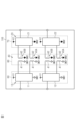
- FIG. 1 is a circuit diagram showing a schematic configuration of a signal transmission device according to an embodiment.
- FIG. 2 is a schematic plan view showing the configuration of the signal transmission device of FIG.
- FIG. 3 is a schematic cross-sectional view showing the configuration of the signal transmission device of FIG.
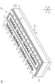
- FIG. 4 is a schematic perspective view showing the insulating chip of FIG.
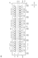
- FIG. 5 is a schematic plan view of the insulating chip of FIG.
- FIG. 6 is a schematic plan view showing an enlarged portion of the insulating chip of FIG.
- FIG. 7 is a schematic plan view showing a first coil of the insulating chip of FIG.
- FIG. 8 is a schematic plan view showing the second coil of the insulating chip of FIG.
- FIG. 1 is a circuit diagram showing a schematic configuration of a signal transmission device according to an embodiment.
- FIG. 2 is a schematic plan view showing the configuration of the signal transmission device of FIG.
- FIG. 3 is a schematic cross-sectional view showing the configuration of the signal transmission
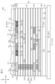
- FIG. 9 is a schematic cross-sectional view of the insulating chip taken along line 9-9 of FIG.
- FIG. 10 is a schematic cross-sectional view of the insulating chip taken along line 10-10 in FIG.
- FIG. 11 is a schematic plan view showing an enlarged portion of the insulating chip of FIG.
- FIG. 12 is a schematic cross-sectional view of the insulating chip taken along line 12-12 of FIG.
- FIG. 13 is a schematic plan view showing the configuration of the first circuit chip in FIG.
- FIG. 14 is a block diagram showing an example of the configuration of a receiving circuit of the signal transmission device of FIG.
- FIG. 15 is a block diagram showing an example of the configuration of the receiving circuit of FIG. FIG.
- FIG. 16 is a circuit diagram showing an example of the configuration of the nonlinear amplifier and envelope detection circuit shown in FIG.
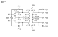
- FIG. 17 is a schematic diagram for explaining the inspection of the insulating chip of FIG.
- FIG. 18 is a schematic plan view showing an enlarged portion of an insulating chip according to a modified example.
- FIG. 19 is a schematic cross-sectional view showing an enlarged portion of the insulating chip taken along line 19-19 in FIG.
- FIG. 20 is a schematic plan view showing an enlarged portion of an insulating chip according to a modified example.
- FIG. 21 is a schematic cross-sectional view showing an enlarged portion of the insulating chip taken along line 21-21 of FIG.
- FIG. 22 is a schematic plan view showing an enlarged portion of an insulating chip according to a modified example.
- FIG. 23 is a schematic cross-sectional view showing an enlarged portion of the insulating chip taken along line 23-23 in FIG.
- FIG. 24 is a schematic plan view showing an enlarged portion of an insulating chip according to a modified example.
- FIG. 25 is an enlarged schematic cross-sectional view of a portion of the insulating chip taken along line 25-25 of FIG.
- FIG. 26 is a schematic plan view showing an enlarged portion of an insulating chip according to a modified example.
- FIG. 27 is a schematic cross-sectional view showing an enlarged portion of the insulating chip taken along line 27-27 in FIG.
- FIG. 28 is a schematic plan view showing an enlarged portion of an insulating chip according to a modified example.
- FIG. 29 is a schematic plan view showing an enlarged portion of an insulating chip according to a modified example.
- FIG. 30 is a schematic plan view showing an enlarged portion of an insulating chip according to a modified example.
- FIG. 31 is a schematic plan view showing an enlarged portion of an insulating chip according to a modified example.
- FIG. 32 is a schematic plan view showing an enlarged portion of an insulating chip according to a modified example.
- FIG. 33 is a schematic cross-sectional view showing a modified insulating tip.
- FIG. 34 is a block diagram showing a receiving circuit of a modified signal transmission device.
- FIG. 35 is a block diagram showing an example of the configuration of the receiving circuit of FIG. FIG.
- FIG. 36 is a circuit diagram showing an example of the configuration of the envelope detection circuit and the adder circuit of FIG.
- FIG. 37 is a waveform diagram showing the operation of the signal transmission device of FIG.
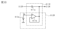
- FIG. 38 is a circuit diagram showing an example of the configuration of the high-pass filter and the DC bias circuit.
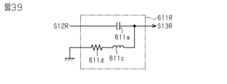
- FIG. 39 is a circuit diagram showing an equivalent circuit of a high-pass filter.
- FIG. 40 is a characteristic diagram showing the output impedance of a buffer.
- FIG. 41 is a waveform diagram showing a modified example of the addition process in the adder circuit.
- FIG. 42 is a schematic plan view showing a configuration of a signal transmission device according to a modified example.
- FIG. 43 is a circuit diagram showing a schematic configuration of a signal transmission device according to a modified example.
- FIG. 43 is a circuit diagram showing a schematic configuration of a signal transmission device according to a modified example.
- FIG. 44 is a schematic plan view showing the configuration of the signal transmission device of FIG. 43.
- FIG. 45 is a schematic plan view showing a configuration of a signal transmission device according to a modified example.
- FIG. 46 is a schematic plan view showing a configuration of a signal transmission device according to a modified example.
- FIG. 47 is a schematic plan view showing a configuration of a signal transmission device according to a modified example.
- At least one means “one or more” of the desired options.
- at least one means “only one option” or “both of two options” if the number of options is two.
- at least one means “only one option” or “any combination of two or more options” if the number of options is three or more.
- FIG. 1 shows a schematic diagram of the circuit configuration of the signal transmission device 100.
- FIG. 2 shows a schematic diagram of an example of the internal configuration (planar structure) of the signal transmission device 100.
- FIG. 3 shows a schematic diagram of an example of the internal configuration (cross-sectional structure) of the signal transmission device 100. Note that hatched lines are omitted in FIG. 3 for the sake of convenience.
- the signal transmission device 100 includes a first circuit chip 60, a second circuit chip 70, and an insulating chip 80.
- the insulating chip 80 is connected between the first circuit chip 60 and the second circuit chip 70.
- the insulating chip 80 provides electrical insulation between the first circuit chip 60 and the second circuit chip 70.
- the first circuit chip 60 includes a first circuit 10 configured to operate with a first voltage V1.
- the first circuit 10 includes a transmitting circuit 11 and a receiving circuit 12.
- the second circuit chip 70 includes a second circuit 20 configured to operate with a second voltage V2.
- the second circuit 20 includes a receiving circuit 21 and a transmitting circuit 22.
- the first voltage V1 and the second voltage V2 may be the same or different.
- the second voltage V2 is equal to the first voltage V1.
- the configuration of the first circuit chip 60 is equal to the configuration of the second circuit chip 70.
- the first circuit chip 60 and the second circuit chip 70 may be referred to as controller chips.
- the signal transmission device 100 may be referred to as a digital isolator.
- the insulating chip 80 includes a plurality of transformers 40.
- the plurality of transformers 40 include a first transformer 40A and a second transformer 40B connected to the transmitting circuit 11 of the first circuit 10, and a third transformer 40A and a fourth transformer 40B connected to the receiving circuit 12 of the first circuit 10.
- the first transformer 40A and the second transformer 40B are electrically connected between the transmitting circuit 11 of the first circuit chip 60 and the receiving circuit 21 of the second circuit chip 70.
- the third transformer 40A and the fourth transformer 40B are electrically connected between the receiving circuit 12 of the first circuit chip 60 and the transmitting circuit 22 of the second circuit chip 70.
- the first to fourth transformers 40A, 40B each include a first coil 41 and a second coil 42.
- the first coil 41 of the first transformer 40A and the second transformer 40B is electrically connected to the transmission circuit 11 of the first circuit chip 60.
- the second coil 42 of the first transformer 40A and the second transformer 40B is electrically connected to the reception circuit 21 of the second circuit chip 70.
- the first coil 41 of the third transformer 40A and the fourth transformer 40B is electrically connected to the reception circuit 12 of the first circuit chip 60.
- the second coil 42 of the third transformer 40A and the fourth transformer 40B is electrically connected to the transmission circuit 22 of the second circuit chip 70.
- the transmitting circuit 11 of the first circuit chip 60 receives an input signal and pulse-drives the first coil 41 of at least one of the first transformer 40A and the second transformer 40B.
- the receiving circuit 21 of the second circuit chip 70 receives a signal excited in the second coil 42 of at least one of the first transformer 40A and the second transformer 40B and outputs an output signal.
- the transmitting circuit 22 of the second circuit chip 70 receives an input signal and pulse-drives the second coil 42 of at least one of the third transformer 40A and the fourth transformer 40B.
- the receiving circuit 12 of the first circuit chip 60 receives a signal excited in the first coil 41 of at least one of the third transformer 40A and the fourth transformer 40B and outputs an output signal.
- FIG. 2 shows an example of the internal configuration of the signal transmission device 100.
- the circuit configuration of the signal transmission device 100 is shown in a simplified manner, so the number of external terminals of the signal transmission device 100 in FIG. 2 is greater than the number of external terminals of the signal transmission device 100 in FIG. 1.
- the external terminals of the signal transmission device 100 include connection terminals to which electronic components external to the signal transmission device 100 can be connected, and power supply terminals to supply power supply voltage to the first circuit chip 60 and the second circuit chip 70 of the signal transmission device 100. Note that terminals that are not connected to the outside may be included as external terminals.
- FIG. 3 shows an example of a cross-sectional view showing the internal configuration of the signal transmission device 100. Note that FIG.
- FIG. 3 is a cross-sectional view showing a simplified internal configuration of the signal transmission device 100.
- the cross-sectional structures of each of the chips 60, 70, and 80 are shown in a simplified manner. For this reason, the cross-sectional structure of the insulating chip 80 shown in FIG. 3 is different from the cross-sectional structure of the insulating chip 80 described later.
- the signal transmission device 100 is a semiconductor device in which a first circuit chip 60, a second circuit chip 70, and an insulating chip 80 are packaged in two packages.
- the package format of the signal transmission device 100 is a small outline (SO) type, and is, for example, a small outline package (SOP).
- the package format of the signal transmission device 100 can be changed as desired.
- the package format is not limited to SOP, and may be a quad for non-lead package (QFN), dual flat package (DFP), dual inline package (DIP), quad flat package (QFP), single inline package (SIP), small outline J-leaded package (SOJ), or various package structures similar to these.
- the first circuit chip 60 is mounted on the first support member 210.
- the second circuit chip 70 is mounted on the second support member 220.
- the insulating chip 80 is mounted on the first support member 210.
- the sealing resin 230 seals the first support member 210 and a portion of the second support member 220 and each of the chips 60, 70, and 80. In FIG. 2, the sealing resin 230 is shown by a two-dot chain line for the convenience of explaining the internal structure of the signal transmission device 100.
- the sealing resin 230 is made of a material having electrical insulation properties. This resin is, for example, a resin containing epoxy resin. This resin may be colored black or the like.
- the sealing resin 230 is formed in a rectangular plate shape with the thickness direction being the Z direction.
- the sealing resin 230 includes four resin side surfaces 231 to 234. More specifically, the sealing resin 230 includes resin side surfaces 231 and 232 as both end faces in the X direction, and resin side surfaces 233 and 234 as both end faces in the Y direction.
- the X direction and the Y direction are directions perpendicular to the Z direction. The X direction and the Y direction are perpendicular to each other.
- the X direction corresponds to the "first direction.”
- the Y direction corresponds to the "second direction.”
- a planar view means a view from the Z direction.
- the first support member 210 and the second support member 220 are each electrically conductive.
- the first support member 210 and the second support member 220 are made of a material containing Cu (copper), Fe (iron), etc.
- Each support member 210, 220 is provided across the inside and outside of the sealing resin 230.
- the first support member 210 includes a first die pad 211 disposed in the sealing resin 230 , and a plurality of first lead terminals 212 disposed across the inside and outside of the sealing resin 230 . Both the first circuit chip 60 and the insulating chip 80 are mounted on the first die pad 211.
- the first die pad 211 is disposed such that its center in the Y direction is closer to the resin side surface 233 than the center in the Y direction of the sealing resin 230.
- the first die pad 211 is not exposed from the sealing resin 230.
- the shape of the first die pad 211 is rectangular with its long side direction in the X direction and its short side direction in the Y direction.
- the multiple first lead terminals 212 are arranged at a distance from each other in the X direction.
- One of the multiple first lead terminals 212, the first lead terminal 212A, is integrated with the first die pad 211.
- a portion of each first lead terminal 212 protrudes outward from the resin side surface 233 of the sealing resin 230.
- the second support member 220 includes a second die pad 221 disposed in the sealing resin 230 , and a plurality of second lead terminals 222 disposed across the inside and outside of the sealing resin 230 .
- the second circuit chip 70 is mounted on the second die pad 221.
- the second die pad 221 is disposed closer to the resin side surface 234 in the Y direction than the first die pad 211.
- the second die pad 221 is not exposed from the sealing resin 230.
- the shape of the second die pad 221 is a rectangle whose long side direction is in the X direction and whose short side direction is in the Y direction.
- the first die pad 211 and the second die pad 221 are arranged to be spaced apart from each other in the Y direction. Therefore, the Y direction can also be said to be the arrangement direction of both die pads 211, 221.
- the dimensions in the Y direction of the first die pad 211 and the second die pad 221 are set depending on the size and number of semiconductor chips to be mounted.
- the first circuit chip 60 and the insulating chip 80 are mounted on the first die pad 211, and the second circuit chip 70 is mounted on the second die pad 221. For this reason, the dimension in the Y direction of the first die pad 211 is larger than the dimension in the Y direction of the second die pad 221.
- the second lead terminals 222 are arranged at a distance from one another in the X direction.
- One of the second lead terminals 222, the second lead terminal 222A, is integrated with the second die pad 221.
- a portion of each second lead terminal 222 protrudes outward from the resin side surface 234 of the sealing resin 230.
- the number of second lead terminals 222 is the same as the number of first lead terminals 212. As can be seen from FIG. 2, the multiple first lead terminals 212 and the multiple second lead terminals 222 are arranged in a direction (X direction) perpendicular to the arrangement direction (Y direction) of the first die pad 211 and the second die pad 221. Note that the number of second lead terminals 222 and the number of first lead terminals 212 can each be changed as desired.
- the first support member 210 and the second support member 220 are composed of a lead frame. During the manufacturing process of the signal transmission device 100, the first die pad 211, the multiple first lead terminals 212, the second die pad 221, and the multiple second lead terminals 222 are formed from the same lead frame.
- the lead frame includes an outer frame formed to surround the first support member 210 and the second support member 220.
- the first lead terminal 212 and the second lead terminal 222 are connected to the outer frame. During the manufacturing process of the signal transmission device 100, the first lead terminal 212 and the second lead terminal 222 are cut off from the outer frame.
- the first die pad 211 is connected to one first lead terminal 212A of the multiple first lead terminals 212.
- the first die pad 211 and the first lead terminal 212A are integrated into one body.
- the first die pad 211 is supported by the first lead terminal 212A.
- the second die pad 221 is connected to one second lead terminal 222A of the multiple second lead terminals 222.
- the second die pad 221 and the second lead terminal 222A are integrated into one body.
- the second die pad 221 is supported by the second lead terminal 222A. Therefore, each die pad 211, 221 does not have a hanging lead exposed from the resin side surface 231, 232. Therefore, the insulation distance (creepage distance) between the first support member 210 and the second support member 220 can be made large.
- the other first lead terminal 212 can be assigned to a signal input/output terminal, etc.
- the second die pad 221 with one second lead terminal 222A the other second lead terminal 222 can be assigned to a signal input/output terminal, etc.
- the first circuit chip 60, the second circuit chip 70, and the insulating chip 80 are arranged at a distance from each other in the Y direction. In the Y direction, the first circuit chip 60, the insulating chip 80, and the second circuit chip 70 are arranged in this order from the first lead terminal 212 to the second lead terminal 222.
- the first circuit chip 60 includes the first circuit 10 shown in FIG. 1. In a plan view, the first circuit chip 60 has a rectangular shape having short and long sides. In a plan view, the first circuit chip 60 is mounted on the first die pad 211 so that the long sides run along the X direction and the short sides run along the Y direction.
- the first circuit chip 60 includes a chip main surface 60s and a chip back surface 60r that face opposite each other in the Z direction.
- the chip back surface 60r of the first circuit chip 60 is bonded to the first die pad 211 by a conductive bonding material SD.
- the conductive bonding material SD may be solder, Ag (silver) paste, or the like.
- a plurality of first electrodes 61, a plurality of second electrodes 62, and a plurality of third electrodes 63 are formed on the chip main surface 60s of the first circuit chip 60.
- the first electrodes 61, the second electrodes 62, and the third electrodes 63 are electrically connected to the first circuit 10.
- the multiple first electrodes 61 are arranged on the chip main surface 60s closer to the first lead terminal 212 than the center of the chip main surface 60s in the Y direction.
- the multiple first electrodes 61 are arranged in the X direction.
- the multiple second electrodes 62 are arranged at both ends of the chip main surface 60s in the X direction.
- the multiple third electrodes 63 are arranged at the end closer to the insulating chip 80 of both ends of the chip main surface 60s in the Y direction.
- the multiple third electrodes 63 are arranged in the X direction.
- the second circuit chip 70 includes the second circuit 20 shown in FIG. 1.
- the shape of the second circuit chip 70 is a rectangle having short and long sides.
- the second circuit chip 70 is mounted on the second die pad 221 so that the long sides run along the X direction and the short sides run along the Y direction.
- the second circuit chip 70 includes a chip main surface 70s and a chip back surface 70r that face opposite each other in the Z direction.
- the chip back surface 70r of the second circuit chip 70 is bonded to the second die pad 221 by a conductive bonding material SD.
- a plurality of first electrodes 71, a plurality of second electrodes 72, and a plurality of third electrodes 73 are formed on the chip main surface 70s of the second circuit chip 70.
- the first electrodes 71, the second electrodes 72, and the third electrodes 73 are electrically connected to the second circuit 20.
- the multiple first electrodes 71 are arranged at the end of the chip main surface 70s in the Y direction that is farther from the insulating chip 80. In other words, the multiple first electrodes 71 are arranged at the end of the chip main surface 70s in the Y direction that is closer to the second lead terminal 222. The multiple first electrodes 71 are arranged in the X direction. The multiple second electrodes 72 are arranged at both ends of the chip main surface 70s in the X direction. The multiple third electrodes 73 are arranged at the end of the chip main surface 70s in the Y direction that is closer to the insulating chip 80. The multiple third electrodes 73 are arranged in the X direction.
- the insulating chip 80 includes the transformer 40 shown in FIG. 1. In a plan view, the insulating chip 80 has a rectangular shape having short and long sides. In a plan view, the insulating chip 80 is mounted on the first die pad 211 so that the long sides are aligned along the X direction and the short sides are aligned along the Y direction.
- the insulating chip 80 is disposed next to the first circuit chip 60 in the Y direction.
- the insulating chip 80 is disposed closer to the second circuit chip 70 than the first circuit chip 60. In other words, the insulating chip 80 is disposed between the first circuit chip 60 and the second circuit chip 70 in the Y direction.
- the insulating chip 80 includes a chip main surface 80s and a chip back surface 80r that face opposite each other in the Z direction.
- the chip back surface 80r of the insulating chip 80 is bonded to the first die pad 211 by a conductive bonding material SD.
- the insulating chip 80 includes a plurality of first electrodes 81 and a plurality of second electrodes 82.
- the first electrodes 81 and the plurality of second electrodes 82 are provided on the chip main surface 80s of the insulating chip 80.
- the plurality of first electrodes 81 are disposed at one of both ends of the insulating chip 80 in the Y direction that is closer to the first circuit chip 60.
- the plurality of first electrodes 81 are arranged in the X direction.
- the plurality of second electrodes 82 are arranged near the center of the insulating chip 80 in the Y direction.
- the plurality of second electrodes 82 are arranged in the X direction.
- the first die pad 211 and the second die pad 221, which are closest to each support member 210, 220, must be spaced apart from each other. Therefore, in a plan view, the distance between the second circuit chip 70 and the insulating chip 80 is greater than the distance between the first circuit chip 60 and the insulating chip 80.
- a number of wires W1 to W4 are connected to each of the first circuit chip 60, the insulating chip 80, and the second circuit chip 70.
- Each of the wires W1 to W4 is a bonding wire formed by a wire bonding device, and is made of a conductor containing, for example, Au (gold), Al (aluminum), Cu, etc.
- the first circuit chip 60 is electrically connected to the first lead terminal 212 by the wire W1. More specifically, the first electrodes 61 and the second electrodes 62 of the first circuit chip 60 are connected to the first lead terminals 212 by the wire W1. The second electrodes 62 of the first circuit chip 60 are connected to one of the first lead terminals 212, the first lead terminal 212A, which is integrated with the first die pad 211, by the wire W1. This electrically connects the first circuit 10 to the first lead terminals 212.
- the first lead terminal 212A integrated with the first die pad 211 constitutes a ground terminal, and the first circuit 10 and the first die pad 211 are electrically connected by the wire W1. Therefore, the first die pad 211 has the same potential as the first ground GND1 of the first circuit 10.
- the second circuit chip 70 and the second lead terminals 222 of the second support member 220 are electrically connected to each other by wires W4. More specifically, the first electrodes 71 and second electrodes 72 of the second circuit chip 70 are connected to the second lead terminals 222 by wires W4. This electrically connects the second circuit 20 to the second lead terminals 222.
- One second lead terminal 222A integrated with the second die pad 221 constitutes a ground terminal, and the second circuit 20 and the second die pad 221 are electrically connected by wires W4. Therefore, the second die pad 221 has the same potential as the second ground GND2 of the second circuit 20.
- the insulating chip 80 is connected to the first circuit chip 60 by wire W2.
- the insulating chip 80 is also connected to the second circuit chip 70 by wire W3. More specifically, the multiple first electrodes 81 of the insulating chip 80 are connected to the multiple third electrodes 63 of the first circuit chip 60 by wire W2.
- the multiple second electrodes 82 of the insulating chip 80 are connected to the multiple third electrodes 73 of the second circuit chip 70 by wire W3.
- the first coils 41 of the transformers 40A and 40B are both electrically connected to the first ground GND1 of the first circuit chip 60 by a wire W2.
- the second coils 42 of the transformers 40A and 40B are electrically connected to the second ground GND2 of the second circuit chip 70 by a wire W3.
- the configuration of the signal transmission device 100 shown in FIG. 1 is an example, and the circuit configurations included in the first circuit chip 60 and the second circuit chip 70 may be changed as appropriate.
- the first circuit 10 may include only the transmitting circuit 11, and the second circuit 20 may include only the receiving circuit 21.
- the first circuit 10 may include circuits other than the transmitting circuit 11 and the receiving circuit 12.
- the second circuit 20 may include circuits other than the receiving circuit 21 and the transmitting circuit 22.
- the first circuit 10 may include an analog-to-digital conversion circuit, in which case the signal transmission device 100 is configured as an isolated A/D conversion device.
- the second circuit 20 may include a driver circuit that drives the gate of the switching element.
- the driver circuit may be connected to a terminal of the signal transmission device 100 (the second lead terminal 222 shown in FIG. 2 as an example).
- the signal transmission device 100 is configured as an insulated gate driver that drives the switching element.
- the switching element may be a power semiconductor element such as a Si Metal-Oxide-Semiconductor Field-Effect Transistor (SiMOSFET), a SiCMOSFET, or an IGBT (Insulated Gate Bipolar Transistor).
- SiMOSFET Si Metal-Oxide-Semiconductor Field-Effect Transistor
- SiCMOSFET SiCMOSFET
- IGBT Insulated Gate Bipolar Transistor
- the signal transmission device 100 used as an insulated gate driver applies a drive voltage signal to the control terminal of a switching element.
- the transmission circuit 11 of the first circuit 10 converts a control signal input from, for example, a control device into a pulse signal.
- the driver circuit of the second circuit 20 outputs a drive voltage signal to the control terminal of the switching element based on a signal received by the reception circuit 21 through transformers 40A, 40B.
- the transmission circuit 22 of the second circuit 20 and the reception circuit 12 of the first circuit 10 may be used to transmit a detection signal from, for example, a temperature sensor arranged near a motor to the control device.
- the first circuit 10 of the signal transmission device 100 used as an insulated gate driver receives a signal from the control device, and the power supply voltage of the first circuit 10 is 5V, 3.3V, etc., with respect to the ground potential.
- the second circuit 20 connected to the high-side switching element a voltage equivalent to the voltage applied to the drain of the high-side switching element (for example, 600V or more) is transiently applied.
- the signal transmission device 100 is required to have a dielectric strength voltage between the first circuit 10 and the second circuit 20, specifically between the first coil 41 and the second coil 42 of the transformers 40A and 40B.
- the required dielectric strength voltage of the signal transmission device 100 is 2500Vrms or more and 7500Vrms or less. In one example, the dielectric strength voltage of the signal transmission device 100 is about 5000Vrms. However, the specific value of the dielectric strength voltage of the signal transmission device 100 is not limited to this and is arbitrary.
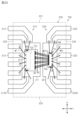
- FIG. 4 is a perspective view showing the appearance of the insulating tip 80.
- FIG. Fig. 5 is a plan view of the insulating chip 80.
- the passivation film 160 is indicated by a two-dot chain line, and the transformers 40A and 40B and dummy wiring 150, which will be described later, are indicated by dashed lines.
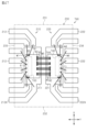
- Fig. 6 is an enlarged plan view showing a part of the insulating chip 80 shown in Fig. 5.
- the transformers 40A and 40B are shown in an enlarged manner.
- Fig. 7 is a cross-sectional view of the insulating chip 80 taken along the XY plane at the Z-direction position of the first coil 41, showing the connection relationship of the first coil 41.
- Fig. 8 is a cross-sectional view of the insulating chip 80 taken along the XY plane at the Z-direction position of the second coil 42, showing the connection relationship of the second coil 42.
- hatching is omitted in Figs. 7 and 8.
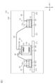
- FIG. 9 is a cross-sectional view of the insulating chip 80 taken along line 9-9 in FIG. 5, showing the cross-sectional structures of the first coil 41, the second coil 42, the dummy wiring 150, the first inner electrode 81A, and the second inner electrode 82A.
- FIG. 10 is a cross-sectional view of the insulating chip 80 taken along line 10-10 in FIG. 5, showing the cross-sectional structures of the dummy wiring 150, the first outer electrode 81C, and the second outer electrode 82C. For convenience, hatching has been omitted for some of the components in FIGS. 9 and 10.
- FIG. 11 is a schematic plan view of an enlarged portion of the insulating chip 80, showing the second inner electrode 82A, the first outer electrode 81C, and the second coil 42.
- FIG. 12 is a cross-sectional view of the insulating chip 80 taken along line 12-12 in FIG. 11, showing the cross-sectional structures of the second coil 42 and the second inner electrode 82A.
- the insulating chip 80 includes four pairs of transformers 40A, 40B. More specifically, the insulating chip 80 is a semiconductor chip in which the four pairs of transformers 40A, 40B are integrated into one chip. In other words, the insulating chip 80 is provided separately from the first circuit chip 60 and the second circuit chip 70 (both of which are shown in FIG. 2).
- the transformers 40A and 40B are disposed near the center of the chip main surface 80s in the Y direction in a plan view.
- the first electrode 81 and the second electrode 82 are electrically connected to the transformers 40A and 40B.
- the second electrode 82 includes a second inner electrode 82A arranged to overlap the inner region 42A of the transformers 40A and 40B in a plan view, and a second outer electrode 82C arranged outside the transformers 40A and 40B.
- the second inner electrode 82A is an electrode connected to the inner end wiring 46A to which the inner end of the second coil 42 is connected
- the second outer electrode 82C is an electrode connected to the outer end wiring 46C to which the outer end of the second coil 42 is connected.
- the second inner electrode 82A and the second outer electrode 82C are made of a material containing one or more appropriately selected from Cu, Al, Ni (nickel), Pd (palladium), and W (tungsten).
- the second inner electrode 82A is electrically connected to each of the transformers 40A and 40B.
- the second electrode 82 includes a second inner electrode 82A connected to the transformer 40A and a second inner electrode 82A connected to the transformer 40B.
- the second outer electrode 82C is disposed between the transformer 40A and the transformer 40B.
- the second outer electrode 82C is electrically connected to the transformer 40A and the transformer 40B. It can be said that the second outer electrode 82C is provided as a common pad for the two transformers 40A and 40B.
- the second inner electrode 82A has a shape in which, in a plan view, its length in the Y direction perpendicular to the X direction is smaller than its length in the X direction in which the second electrodes 82 are arranged.
- the shape of the second inner electrode 82A is a rectangle that is longer in the X direction.
- the second outer electrode 82C has a shape in which its length in the X direction in which the second electrodes 82 are arranged is equal to its length in the Y direction.
- the shape of the second outer electrode 82C is a square.
- the first electrodes 81 are arranged such that two of them are aligned with one transformer 40A in the X direction, two are aligned with one transformer 40B in the X direction, and one is located between the transformers 40A and 40B in the X direction.
- the first electrodes 81 are arranged closer to the chip side surface 802 than the transformers 40A and 40B in the Y direction. In other words, the first electrodes 81 are arranged between the transformers 40A and 40B and the chip side surface 802 in the Y direction.
- the first electrodes 81 can also be said to be arranged closer to the first lead terminal 212 (see FIG. 2) than the transformers 40A and 40B.
- the first electrode 81 includes a first inner electrode 81A corresponding to the second inner electrode 82A of the second electrode 82, and a first outer electrode 81C corresponding to the second outer electrode 82C of the second electrode 82.
- the first inner electrode 81A is an electrode connected to the inner end wiring 44A, i.e., the inner end of the first coil 41
- the first outer electrode 81C is an electrode connected to the outer end wiring 44C, i.e., the outer end of the first coil 41.
- the first inner electrode 81A and the first outer electrode 81C are made of a material containing one or more appropriately selected from Cu, Al, Ni, Pd, and W.
- the first inner electrode 81A is electrically connected to each of the transformers 40A and 40B.
- the insulating chip 80 includes a first inner electrode 81A electrically connected to the transformer 40A and a first inner electrode 81A electrically connected to the transformer 40B.
- the first outer electrode 81C is electrically connected to the transformer 40A and the transformer 40B.
- the first outer electrode 81C can be said to be provided as a common pad for the two transformers 40A and 40B.
- the first inner electrode 81A has a shape in which, in a plan view, its length in the Y direction perpendicular to the X direction is smaller than its length in the X direction in which the first electrodes 81 are arranged.
- the shape of the first inner electrode 81A is a rectangle that is longer in the X direction.
- the first outer electrode 81C has a shape in which its length in the X direction in which the second electrodes 82 are arranged is equal to its length in the Y direction.
- the shape of the first outer electrode 81C is a square.
- the first inner electrode 81A is arranged in a position overlapping with the transformers 40A and 40B when viewed from the Y direction.
- the first outer electrode 81C is arranged in a position overlapping with the portion between the transformers 40A and 40B in the X direction when viewed from the Y direction. Therefore, the multiple first electrodes 81 (81A, 81C) are aligned with each other in the Y direction and spaced apart from each other in the X direction.
- transformer 40B Each pair of transformers 40A, 40B have the same configuration. Furthermore, transformer 40B is configured in the same manner as transformer 40A. Therefore, the detailed structure of transformer 40A will be described, and a description of transformer 40B will be omitted.
- the insulating chip 80 includes four chip side surfaces 801, 802, 803, and 804 that are orthogonal to both the chip main surface 80s and the chip back surface 80r.
- the chip side surfaces 801 to 804 are provided between the chip main surface 80s and the chip back surface 80r in the Z direction.
- the chip side surfaces 801 and 802 constitute both end surfaces of the insulating chip 80 in the Y direction
- the chip side surfaces 803 and 804 constitute both end surfaces of the insulating chip 80 in the X direction.
- the chip side surfaces 801 and 802 constitute the long sides of the insulating chip 80
- the chip side surfaces 803 and 804 constitute the short sides of the insulating chip 80.
- the chip side surface 801 is closer to the second circuit chip 70 (see FIG. 2) than the chip side surface 802, and the chip side surface 802 is closer to the first circuit chip 60 (see FIG. 2) than the chip side surface 801.
- the insulating chip 80 includes a substrate 83 and an insulating layer 84 formed on the substrate 83.
- the substrate 83 is, for example, a semiconductor substrate.
- the substrate 83 is a substrate formed from a material containing Si (silicon).
- Examples of the Si substrate used for the substrate 83 include a semiconductor substrate made of a single crystal intrinsic semiconductor material, a p-type semiconductor substrate containing an acceptor-type impurity, and an n-type semiconductor substrate containing a donor-type impurity.
- the substrate 83 may be an epitaxial substrate including a Si substrate and an epitaxial layer stacked on the Si substrate.
- a functional device may be formed on the substrate 83.
- the functional device may include a passive element such as a resistor, an active element such as a transistor, a circuit network composed of a plurality of elements, and the like.
- the substrate 83 may be a semiconductor substrate made of a wide bandgap semiconductor or a compound semiconductor. Alternatively, the substrate 83 may be an insulating substrate made of a material containing glass, instead of a semiconductor substrate.
- the wide bandgap semiconductor is a semiconductor substrate having a bandgap of 2.0 eV or more.
- the wide bandgap semiconductor may be SiC (silicon carbide), GaN (gallium nitride), Ga2O3 (gallium oxide), or the like.
- the compound semiconductor may be a III-V compound semiconductor.
- the compound semiconductor may include at least one of AlN (aluminum nitride), InN (indium nitride), GaN, and GaAs (gallium arsenide).
- the substrate 83 includes a substrate main surface 83s and a substrate back surface 83r that face in opposite directions in the Z direction.
- the substrate back surface 83r constitutes a chip back surface 80r of the insulating chip 80.
- the insulating layer 84 includes an upper surface 84s and a lower surface 84r facing opposite to the upper surface 84s.
- the insulating layer 84 includes a plurality of insulating films 85 stacked in the Z direction from the substrate main surface 83s of the substrate 83.
- the Z direction can also be said to be the thickness direction of the insulating layer 84.
- the Z direction can also be said to be the stacking direction of the insulating films 85.
- the insulating layer 84 is formed on the substrate main surface 83s of the substrate 83.
- the insulating film 85 includes a first insulating film 85A and a second insulating film 85B formed on the first insulating film 85A.
- the first insulating film 85A is a thin film, for example, an etching stopper layer.
- the first insulating film 85A is formed of a material including SiN (silicon nitride), SiC, SiCN (nitrogen-added silicon carbide), or the like.
- the first insulating film 85A is formed of a material including SiN.
- the second insulating film 85B is, for example, an interlayer insulating film.
- the second insulating film 85B is formed of a material including SiO 2 (silicon oxide).
- the thickness of the second insulating film 85B is thicker than the thickness of the first insulating film 85A.
- the thickness of the first insulating film 85A may be 100 nm or more and less than 1000 nm.
- the thickness of the second insulating film 85B may be 1000 nm or more and 3000 nm or less.
- the thickness of the first insulating film 85A is, for example, about 300 nm, and the thickness of the second insulating film 85B is, for example, about 2000 nm.
- the bottom insulating film 85L in contact with the substrate main surface 83s of the substrate 83 and the top insulating film 85U are both composed of the second insulating film 85B.
- the thicknesses of both the bottom insulating film 85L and the top insulating film 85U are thinner than the other insulating films 85.
- the thicknesses of both the bottom insulating film 85L and the top insulating film 85U are greater than or equal to the thickness of the first insulating film 85A and less than or equal to the thickness of the second insulating film 85B.
- the thickness of both the bottom insulating film 85L and the top insulating film 85U can be changed as desired.
- the thickness of both the bottom insulating film 85L and the top insulating film 85U may be thicker than the thickness of the second insulating film 85B, or may be greater than or equal to the thickness of the insulating film 85 formed by the first insulating film 85A and the second insulating film 85B.
- the first coil 41 of the transformers 40A and 40B is composed of a first coil wiring 43.
- the shape of the first coil wiring 43 is annular in a plan view, and in one example, is a circular spiral shape.
- the first coil 41 is composed of a material including one or more appropriately selected from Ti (titanium), TiN (titanium nitride), Au, Ag, Cu, Al, and W.
- a first inner end wiring 44A is arranged inside the first coil wiring 43, and a first outer end wiring 44C is arranged outside the first coil wiring 43.
- One end of the first coil wiring 43 is electrically connected to the first inner end wiring 44A, and the other end of the first coil wiring 43 is electrically connected to the first outer end wiring 44C.
- the first inner end wiring 44A and the first outer end wiring 44C are made of a material containing one or more appropriately selected from Ti, TiN, Au, Ag, Cu, Al, and W.
- the first outer end wiring 44C is configured as a common end wiring for the first coils 41 of the transformers 40A and 40B. It is also possible to provide an outer end wiring for each of the first coils 41 of the transformers 40A and 40B.
- connection wiring 131A is made of a material containing one or more appropriately selected from Ti, TiN, Au, Ag, Cu, Al, and W.
- the connection wiring 131A includes a first wiring portion 132A extending in the Z direction so as to penetrate a plurality of insulating films 85, and a second wiring portion 136A extending in the Y direction.
- the first wiring portion 132A is disposed at a position overlapping the first inner electrode 81A in a plan view, and is connected to the first inner electrode 81A.
- the first wiring portion 132A penetrates from the insulating film 85 below the uppermost insulating film 85U to the insulating film 85 two layers above the lowermost insulating film 85L among the multiple insulating films 85.
- the first wiring portion 132A includes flat wiring portions 133A and 134A and multiple vias 135A.
- the wiring portions 133A and 134A are provided at the same positions as the insulating films 851 and 852 on which the coils 41 and 42 are provided.
- the vias 135A are provided between the two wiring portions in the Z direction, between the upper wiring portion 134A and the first inner electrode 81A, and between the lower wiring portion 133A and the second wiring portion 136A.
- the wiring portions 133A and 134A are formed of the same conductive material as the first coil 41 and the second coil 42.
- the second wiring portion 136A is provided closer to the substrate 83 than the first wiring portion 132A.
- the second wiring portion 136A is provided closer to the substrate 83 than the first coil 41.
- the second wiring portion 136A is provided in an insulating film 85 that is one layer above the lowest insulating film 85L among the multiple insulating films 85.
- the first end closer to the chip side surface 802 of the insulating chip 80 is provided at a position overlapping the first wiring portion 132A in a planar view.
- the second wiring portion 136A is connected to the first wiring portion 132A.
- the second end opposite the first end is provided at a position overlapping the first coil 41 of the transformer 40A in a planar view.
- the second end is provided at a position overlapping the first inner end wiring 44A to which the first coil 41 of the transformer 40A is connected in a planar view.
- the second wiring portion 136A includes a plurality of vias 137A that connect the second wiring portion 136A and the first inner end wiring 44A.
- connection wiring 131C is made of a material containing one or more appropriately selected from Ti, TiN, Au, Ag, Cu, Al, and W.
- connection wiring 131C includes a first wiring portion 132C extending in the Z direction so as to penetrate a plurality of insulating films 85, and a second wiring portion 136C extending in the Y direction.
- the first wiring portion 132C is configured similarly to the first wiring portion 132A of the connection wiring 131A.
- the first wiring portion 132C is disposed at a position overlapping the first outer electrode 81C in a plan view, and is connected to the first outer electrode 81C.
- the first wiring portion 132C penetrates from the insulating film 85 below the uppermost insulating film 85U to the insulating film 85 two layers above the lowermost insulating film 85L among the multiple insulating films 85.
- the first wiring portion 132C has flat wiring portions 133C, 134C and multiple vias 135C.
- the wiring portions 133C, 134C are provided at the same positions as the insulating films 851, 852 on which the coils 41, 42 are provided.
- the vias 135C are provided between the two wiring portions in the Z direction, between the upper wiring portion and the first outer electrode 81C, and between the lower wiring portion and the second wiring portion 136C.
- the wiring portions 133C, 134C are formed of the same conductive material as the first coil 41 and the second coil 42.
- the second wiring portion 136C is provided closer to the substrate 83 than the first wiring portion 132C.
- the second wiring portion 136C is provided closer to the substrate 83 than the first coil 41.
- the second wiring portion 136C is provided in an insulating film 85 that is one layer above the lowest insulating film 85L among the multiple insulating films 85.
- the first end closer to the chip side surface 802 of the insulating chip 80 is provided at a position overlapping the first wiring portion 132C in a planar view.
- the second wiring portion 136C is connected to the first wiring portion 132C.
- the second end opposite the first end is provided at a position that does not overlap the first coil 41 of the transformer 40A in a planar view.
- the second end is provided at a position that overlaps the first outer end wiring 44C to which the first coil 41 of the transformer 40A is connected in a planar view.
- the second wiring portion 136C has a plurality of vias 137C that connect the second wiring portion 136C and the first outer end wiring 44C.
- the second wiring portion 136C of the connection wiring 131C is electrically connected to the substrate 83 by vias 138 that penetrate the insulating film 85L of the lowest layer. Note that the vias 138 may be omitted.
- the second coil 42 of the transformer 40A, 40B includes a second coil wiring 45.
- the shape of the second coil wiring 45 is annular in a plan view, and in one example, is a circular spiral shape.
- the second coil 42 is made of a material including one or more appropriately selected from Ti, TiN, Au, Ag, Cu, Al, and W.
- a second inner end wiring 46A is arranged in the inner region 42A surrounded by the second coil wiring 45, and a second outer end wiring 46C is arranged outside the second coil wiring 45.
- One end of the second coil wiring 45 is electrically connected to the second inner end wiring 46A, and the other end of the second coil wiring 45 is electrically connected to the second outer end wiring 46C.
- the second inner end wiring 46A and the second outer end wiring 46C are made of a material containing one or more appropriately selected from Ti, TiN, Au, Ag, Cu, Al, and W.
- the second outer end wiring 46C is configured as a common end wiring for the second coils 42 of the transformers 40A and 40B. Note that the second outer end wiring 46C may be provided for each of the second coils 42 of the transformers 40A and 40B.
- the second coil wiring 45 is formed in the same winding direction as the first coil wiring 43 shown in FIG. 7 when viewed in a plan view.
- the number of turns of the second coil wiring 45 is the same as the number of turns of the first coil wiring 43. Note that the number of turns of the second coil wiring 45 and the number of turns of the first coil wiring 43 may be different.
- the first coil 41 and the second coil 42 of the transformer 40A are arranged opposite each other in the Z direction via an insulating film 85.
- the first coil 41 and the second coil 42 are arranged opposite each other in the Z direction via multiple insulating films 85.
- the second coil 42 is configured as a conductive layer embedded in one insulating film 85. More specifically, the insulating film 852 in which the second coil 42 is embedded has a wiring groove (second wiring groove) 142 that penetrates both the first insulating film 85A and the second insulating film 85B in the Z direction. The conductive layer that constitutes the second coil 42 is embedded in the wiring groove 142 of the insulating film 852. The insulating film 852 in which the second coil 42 is embedded is covered by the insulating film 85 that is adjacent to the insulating film 852 in the Z direction. As a result, it can be said that the second coil 42 is embedded in the insulating film 85.
- the second coil 42 is located farther from the substrate 83 than the first coil 41.
- the second coil 42 can be said to be located higher than the first coil 41.
- the first coil 41 can be said to be disposed closer to the substrate 83 than the second coil 42.
- the distance D1 between the first coil 41 and the second coil 42 in the Z direction is greater than the distance between the first coil 41 and the substrate main surface 83s of the substrate 83.
- the first outer electrode 81C is formed on the top insulating film 85U.
- the first outer electrode 81C is formed on the upper surface 84s of the insulating layer 84.
- the first outer electrode 81C is electrically connected to the wiring portion 134C of the first wiring portion 132C by a via 91C that penetrates the insulating film 85U.
- the second outer electrode 82C is formed on the top insulating film 85U.
- the second outer electrode 82C is formed on the upper surface 84s of the insulating layer 84.
- the second outer electrode 82C is electrically connected to the second outer end wiring 46C by a via 92C that penetrates the insulating film 85U.
- the dummy wiring 150 includes a first dummy wiring 151, a second dummy wiring 152, and a third dummy wiring 153.
- the first dummy wiring 151, the second dummy wiring 152, and the third dummy wiring 153 are formed from a material containing one or more appropriately selected from Ti, TiN, Au, Ag, Cu, Al, and W.
- the first dummy wiring 151 is disposed in the same position as the second dummy wiring 152 and the third dummy wiring 153 in the Z direction. As shown in FIG. 9, the second dummy wiring 152 and the third dummy wiring 153 are disposed in the same position as the second coil 42 in the Z direction. Therefore, although not shown, the first dummy wiring 151 is disposed in the same position as the second coil 42 in the Z direction. In other words, the first dummy wiring 151 is disposed in a position farther from the substrate 83 than the first coil 41. In other words, it can be said that the dummy wiring 150 is provided around the coil of the transformer 40A, 40B that is closer to the chip main surface 80s of the insulating chip 80. By making the first dummy wiring 151 have the same voltage as the second coil 42, the voltage drop between the second coil 42 and the first dummy wiring 151 can be suppressed. Therefore, the electric field concentration on the second coil 42 can be suppressed.
- the fourth dummy wiring 154 is disposed between the second coil 42 and the first electrode 81 in a planar view.
- the fourth dummy wiring 154 extends along the X direction.
- the fourth dummy wiring 154 is formed along the multiple first electrodes 81 in a planar view.
- the fourth dummy wiring 154 may include multiple wires.
- the fourth dummy wiring 154 is electrically independent from the second coil 42. In other words, the fourth dummy wiring 154 is not electrically connected to the second coil 42.
- the fourth dummy wiring 154 separates each of the multiple first electrodes 81 from the second coil 42.
- the first electrode 81 and the second electrode 82 are covered by a passivation film 160.
- the passivation film 160 has openings that expose parts of the first electrode 81 and the second electrode 82.
- the first electrode 81 has an exposed surface for connecting the wire W2.
- the second electrode 82 has an exposed surface for connecting the wire W3.
- the openings in the passivation film 160 are indicated by two-dot chain lines.
- the first electrode 81 includes a first inner electrode 81A and a first outer electrode 81C.
- the passivation film 160 includes a first inner opening 161 exposing a portion of the first inner electrode 81A and a first outer opening 162 exposing a portion of the first outer electrode 81C.
- the first inner electrode 81A has a rectangular shape that is longer in the X direction than in the Y direction.
- the passivation film 160 includes two first inner openings 161 that expose a portion of the first inner electrode 81A.
- the two first inner openings 161 are arranged in the X direction according to the shape of the first inner electrode 81A.
- each of the two first inner openings 161 is formed in a square shape with the same length in the X direction and the same length in the Y direction.
- the first inner electrode 81A includes two exposed surfaces exposed by two first inner openings 161 of the passivation film 160. The two exposed surfaces of the first inner electrode 81A become first pads P1 for connecting the first coil 41 to the outside.
- the first inner electrode 81A includes two first pads P1 by the two first inner openings 161.
- the first outer electrode 81C is formed in a square shape with the length in the Y direction and the length in the X direction being equal.
- the passivation film 160 includes one first outer opening 162 that exposes a portion of the first outer electrode 81C.
- the first outer opening 162 is formed in a square shape with the length in the X direction and the length in the Y direction being equal, depending on the shape of the first outer electrode 81C. In one example, the size of the first outer opening 162 is equal to the size of the first inner opening 161.
- the first outer electrode 81C includes an exposed surface exposed by a first outer opening 162 of the passivation film 160.
- the exposed surface of the first outer electrode 81C serves as a second pad P2 for externally connecting the first coil 41.
- the first outer electrode 81C includes a second pad P2 by the first outer opening 162.
- the second electrode 82 includes a second inner electrode 82A and a second outer electrode 82C.
- the passivation film 160 includes a second inner opening 163 that exposes a portion of the second inner electrode 82A, and a second outer opening 164 that exposes a portion of the first outer electrode 81C.
- the second inner opening 163 corresponds to the second opening.
- the second inner electrode 82A has a rectangular shape that is longer in the X direction than in the Y direction.
- the passivation film 160 includes two second inner openings 163 that expose parts of the second inner electrode 82A.
- the two second inner openings 163 are arranged in the X direction according to the shape of the second inner electrode 82A.
- each of the two second inner openings 163 is formed in a square shape whose length in the X direction and length in the Y direction are equal.
- the second inner electrode 82A includes two exposed surfaces exposed by the two second inner openings 163 of the passivation film 160.
- the two exposed surfaces of the second inner electrode 82A become third pads P3 for externally connecting the second coil 42.
- the second inner electrode 82A includes two third pads P3 by the two second inner openings 163.
- the second outer electrode 82C is formed in a square shape with the length in the Y direction and the length in the X direction being equal.
- the passivation film 160 includes one second outer opening 164 that exposes a portion of the second outer electrode 82C.
- the second outer opening 164 is formed in a square shape with the length in the X direction and the length in the Y direction being equal, depending on the shape of the second outer electrode 82C. In one example, the size of the second outer opening 164 is equal to the size of the first inner opening 161.
- the second outer electrode 82C includes an exposed surface exposed by one second outer opening 164 of the passivation film 160.
- the exposed surface of the second outer electrode 82C serves as a fourth pad P4 for externally connecting the second coil 42.
- the second outer electrode 82C includes a fourth pad P4 by way of one second outer opening 164.
- the insulating chip 80 includes a resin layer 170 formed on a passivation film 160.
- the resin layer 170 is formed of a material containing, for example, polyimide (PI).
- the resin layer 170 is separated into an inner resin layer and an outer resin layer by a separation groove 173. As shown in FIG. 4, in a plan view, the separation groove 173 is formed so as to surround the transformers 40A and 40B.
- the resin layer 170 includes a first resin opening 174 that exposes the first electrode 81, and a second resin opening 175 that exposes the second electrode 82.
- the second inner electrode 82A is formed in a rectangular shape whose length in the X direction is longer than its length in the Y direction in a plan view. is disposed so as to overlap with the inner end wiring 46A in plan view.
- the second inner electrode 82A is electrically connected to the inner end wiring 46A.
- the second inner electrode 82A is arranged so as to overlap the inner region 42A surrounded by the second coil 42 in a plan view.
- the inner region 42A has a circular shape formed by the circular spiral shape of the second coil 42 (second coil wiring 45).
- the second inner electrode 82A has a rectangular shape that is long in the X direction in which the second coil 42 of the insulating chip 80 is arranged.
- the length L2 of the second inner electrode 82A in the X direction is greater than the dimension L1 of the inner region 42A surrounded by the second coil 42 in the X direction. It can be said that the dimension of the inner region 42A surrounded by the second coil 42 in the X direction is smaller than the length of the second inner electrode 82A in the X direction. Therefore, both ends 82AA, 82AB of the second inner electrode 82A overlap with the second coil 42 in a planar view.
- This second inner electrode 82A includes a first overlapping portion 82A1 that overlaps with the inner region 42A surrounded by the second coil 42 and a second overlapping portion 82A2 that overlaps with the second coil 42 in a planar view.
- the first overlapping portion 82A1 corresponds to the first region.
- the second overlapping portion 82A2 corresponds to the second region.
- the second inner electrode 82A can be said to be disposed across both the inner region 42A and the region 42B that overlaps with the second coil 42. In one example, the area of the second overlapping portion 82A2 is larger than the area of the first overlapping portion 82A1.
- the passivation film 160 includes two second inner openings 163 that expose a portion of the second inner electrode 82A.
- the two second inner openings 163 are each formed on the second inner electrode 82A at a position that spans both the inner region 42A and the region that overlaps with the second coil 42.
- the second outer electrode 82C is formed in a square shape with the same length in the X direction and the Y direction in a plan view.
- the second outer electrode 82C is disposed between two second coils 42 aligned in the X direction.
- the two second coils 42 can be said to be disposed on either side of the second outer electrode 82C, which has a length shorter than the length of the second inner electrode 82A in the X direction.
- the first inner electrode 81A is formed in a rectangular shape in which the length in the X direction is longer than the length in the Y direction in a plan view.
- the length of the inner electrode 81A is equal to the length of the second inner electrode 82A in the X direction.
- the first inner electrode 81A is disposed at the same position as the second inner electrode 82A in the X direction.
- the first outer electrode 81C is formed in a square shape with the same length in the Y direction and the same length in the X direction in a plan view. In one example, the length of the first outer electrode 81C in the X direction is equal to the length of the second outer electrode 82C in the X direction. The first outer electrode 81C is disposed in the same position as the second outer electrode 82C in the X direction.
- first circuit chip 60 and the second circuit chip 70 Next, the first circuit chip 60 and the second circuit chip 70 will be described.
- the first circuit chip 60 and the second circuit chip 70 have the same configuration. Therefore, the first circuit chip 60 will be described below, and a description of the second circuit chip 70 will be omitted.
- FIG. 13 is a plan view showing the configuration of the first circuit chip 60. Note that in FIG. 13, for the purpose of explanation, the functional blocks and wiring included in the first circuit chip 60 are shown with solid lines, and it is not intended that they are arranged above the first to third electrodes 61 to 63.
- the first circuit chip 60 has a rectangular parallelepiped shape whose length in the X direction is longer than its length in the Y direction.
- the first circuit chip 60 includes a chip main surface 60s and a chip back surface 60r that face opposite each other in the Z direction.
- the first circuit chip 60 also includes four chip side surfaces 601, 602, 603, and 604 that are perpendicular to both the chip main surface 60s and the chip back surface 60r.
- the chip side surfaces 601 and 602 form both end surfaces of the first circuit chip 60 in the Y direction
- the chip side surfaces 603 and 604 form both end surfaces of the first circuit chip 60 in the X direction.
- chip side surfaces 601 and 602 form the long sides of the first circuit chip 60, and the chip side surfaces 603 and 604 form the short sides of the first circuit chip 60.
- chip side 601 is closer to insulating chip 80 than chip side 602, and chip side 602 is closer to first lead terminal 212 shown in FIG. 2 than chip side 601.
- the first circuit chip 60 includes a plurality of first electrodes 61, a plurality of second electrodes 62, and a plurality of third electrodes 63 formed on the chip main surface 60s.
- the plurality of first electrodes 61 are arranged along the chip side surface 602 on the chip main surface 60s.
- the plurality of second electrodes 62 are arranged along the chip side surfaces 603, 604 on the chip main surface 60s.
- the plurality of third electrodes 63 are arranged along the chip side surface 601 on the chip main surface 60s.
- the first circuit chip 60 includes, as functional blocks, transmitting circuits 11A, 11B and receiving circuits 12A, 12B.
- the receiving circuits 12A, 12B and the transmitting circuits 11A, 11B are arranged between a first electrode 61 and a third electrode 63. In the first circuit chip 60, they are arranged from chip side surface 603 to chip side surface 604.
- the multiple first electrodes 61 are electrically connected to the transmitting circuits 11A and 11B.
- the transmitting circuits 11A and 11B input a pulse signal from the connected first electrodes 61.
- the multiple first electrodes 61 are connected to the receiving circuits 12A and 12B.
- the receiving circuits 12A and 12B output a pulse signal toward the connected first electrodes 61.
- the second electrodes 62 include ground pads 62G1, 62G2 electrically connected to the first ground GND1 (see FIG. 1) of the transmitting circuits 11A, 11B and the receiving circuits 12A, 12B.
- the ground pads 62G1, 62G2 correspond to ground pads.
- the second electrodes 62 also include power supply pads 62V1, 62V2 that supply a first voltage (see FIG. 1) to the transmitting circuits 11A, 11B and the receiving circuits 12A, 12B.
- the third electrodes 63 include a transmitting pad 63A electrically connected to the transmitting circuits 11A and 11B, and a receiving pad 63B electrically connected to the receiving circuits 12A and 12B.
- the third electrodes 63 also include a ground pad 63C electrically connected to the ground pads 62G1 and 62G2.
- the two transmitting pads 63A connected to the transmitting circuits 11A and 11B are arranged with the ground pad 63C in between.
- the two receiving pads 63B connected to the receiving circuits 12A and 12B are arranged with the ground pad 63C in between.
- the transmitting pad 63A and the receiving pad 63B correspond to signal pads.
- the insulating chip 80 includes three ground wirings 64A, 64B, and 64C.
- the three ground wirings 64A, 64B, and 64C are electrically connected between the two ground pads 62G1 and 62G2.
- the first ground wiring 64A and the second ground wiring 64B correspond to the first ground wiring.
- the third ground wiring 64C corresponds to the second ground wiring.
- the first ground wiring 64A corresponds to the receiving ground wiring.
- the second ground wiring 64B corresponds to the transmitting ground wiring.
- the three ground wirings 64A to 64C may be electrically connected to either the ground pad 62G1 or the ground pad 62G2.
- the three ground wirings 64A to 64C are arranged at a distance from each other between the two ground pads 62G1 and 62G2. In other words, the three ground wirings 64A to 64C are laid on different paths between the two ground pads 62G1 and 62G2. Each of the three ground wirings 64A to 64C is an independent wiring.
- the receiving circuits 12A and 12B are electrically connected to the first ground wiring 64A.
- the transmitting circuits 11A and 11B are electrically connected to the second ground wiring 64B.
- the ground pads 63C included in the multiple third electrodes 63 are electrically connected to the third ground wiring 64C.
- the ground wiring is the first ground GND1 shown in FIG. 1.
- the transmission circuit 11A drives the first coil 41 of the transformers 40A and 40B with an input pulse signal
- the operation of the transmission circuit 11A may cause a potential fluctuation in the first ground GND1.
- the transmission circuits 11A and 11B and the reception circuits 12A and 12B share a common ground wiring, the potential of the first ground GND1 of the reception circuits 12A and 12B changes. This potential change may cause a malfunction in the reception circuits 12A and 12B.
- the potential fluctuation of the first ground GND1 becomes a potential fluctuation of the ground pad 63C, which affects the reception signal by the first coil 41 of the transformers 40A and 40B. In other words, errors may occur in the reception signal and the output pulse signal in the reception circuits 12A and 12B. This leads to a deterioration in the transmission characteristics.
- the potential fluctuation of the first ground GND1 can also occur due to the operation of the receiving circuits 12A and 12B. In this case, the potential fluctuation of the first ground GND1 can cause the transmitting circuits 11A and 11B to malfunction and cause errors in the drive signals output by the transmitting circuits 11A and 11B.
- the transmitter circuits 11A, 11B, receiver circuits 12A, 12B, and ground pad 63C are electrically connected to the ground pads 62G1, 62G2 by first to third ground wirings 64A to 64C that are independent of each other. Therefore, the receiver circuits 12A, 12B are less susceptible to potential fluctuations in the first ground GND1 caused by the operation of the transmitter circuits 11A, 11B. In addition, the transmitter circuits 11A, 11B are less susceptible to potential fluctuations in the first ground GND1 caused by the operation of the receiver circuits 12A, 12B. The effects on the drive signal and output pulse signal can be reduced. This can improve the transmission characteristics of the signal transmission device 100.
- Fig. 14 shows an outline of the electrical configuration of the signal transmission device 100.
- Fig. 14 shows the transmitting circuit 11 of the first circuit chip 60, the transformers 40A and 40B of the insulating chip 80, and the receiving circuit 21 of the second circuit chip 70 shown in Fig. 1.
- the transmitting circuit 22 of the second circuit chip 70 and the receiving circuit 12 of the first circuit chip 60 shown in Fig. 1 are similar, so drawings and explanations thereof will be omitted.
- the transmission circuit 11 outputs a transmission pulse signal S1 to the transformers 40A and 40B in response to the input pulse signal Din.
- the transformers 40A and 40B provide insulation between the transmission circuit 11 and the reception circuit 21, and transmit the transmission pulse signal S1 as a reception pulse signal S2.
- the reception circuit 21 outputs an output pulse signal Dout in response to the reception pulse signal S2 from the transformers 40A and 40B.
- the receiving circuit 21 includes a high-pass filter 301 , a DC bias circuit 302 , a non-linear amplifier 303 , an envelope detection circuit 304 , a subtraction circuit 305 , and a comparison circuit 306 .
- the high-pass filter 301 generates a filtered received pulse signal S3 by blocking low-frequency components of the received pulse signal S2 that are lower than the cutoff frequency fc and passing high-frequency components that are higher than the cutoff frequency fc.
- the DC bias circuit 302 is connected to the output terminal of the high-pass filter 301 and sets the DC bias of the filtered received pulse signal S3.
- the nonlinear amplifier 303 amplifies the filtered received pulse signal S3 in a nonlinear region to generate an amplified received pulse signal S4.
- the envelope detection circuit 304 detects the envelope of the amplified received pulse signal S4 to generate an envelope signal S5.
- the subtraction circuit 305 takes measures against undershoot of the envelope signal S5.
- the subtraction circuit 305 generates a subtraction envelope signal S6 in response to the envelope signal S5.
- the comparator circuit 306 compares the subtracted envelope signal S6 with a predetermined threshold value to generate an output pulse signal Dout.
- FIG. 15 shows an example of a detailed electrical configuration of the signal transmission device 100.
- the signal transmission device 100 generates a first signal triggered by the rising edge of the input pulse signal Din and a second signal triggered by the falling edge of the input pulse signal Din, processes the first signal and the second signal, and outputs the output pulse signal Dout.
- each of the signals S1 to S6 shown in FIG. 14 includes a signal corresponding to the first signal and the second signal.
- signals corresponding to the first signal are marked with "R” and signals corresponding to the second signal are marked with "F”.
- the transmission circuit 11 receives the input pulse signal Din and generates a first transmission pulse signal S1R and a second transmission pulse signal S1F.
- the transmission circuit 11 generates the first transmission pulse signal S1R using the rising edge of the input pulse signal Din as a trigger.
- the first transmission pulse signal S1R may include one or more pulses.
- the transmission circuit 11 also generates the second transmission pulse signal S1F using the falling edge of the input pulse signal Din as a trigger.
- the second transmission pulse signal S1F may include one or more pulses.
- the receiving circuit 21 processes the first receiving pulse signal S2R and the second receiving pulse signal S2F output from the transformers 40A and 40B to generate an output pulse signal Dout. For example, the receiving circuit 21 outputs a high-level output pulse signal Dout in response to the pulse driving of the first receiving pulse signal S2R. Also, for example, the receiving circuit 21 outputs a low-level output pulse signal Dout in response to the pulse driving of the second receiving pulse signal S2F.
- the transformers 40A and 40B transmit the first transmission pulse signal S1R as the first reception pulse signal S2R while providing insulation between the transmission circuit 11 and the reception circuit 21.
- the transformers 40A and 40B transmit the second transmission pulse signal S1F as the second reception pulse signal S2F while providing insulation between the transmission circuit 11 and the reception circuit 21.
- the receiving circuit 21 includes high-pass filters 301R and 301F, DC bias circuits 302R and 302F, nonlinear amplifiers 303R and 303F, envelope detection circuits 304R and 304F, a subtraction circuit 305, and a comparison circuit 306.
- the high-pass filter 301R generates a first filtered received pulse signal S3R by blocking low-frequency components lower than the cutoff frequency fc and passing high-frequency components higher than the cutoff frequency fc among the frequency components of the first received pulse signal S2R.
- the high-pass filter 301F generates a second filtered received pulse signal S3F by blocking low-frequency components lower than the cutoff frequency fc and passing high-frequency components higher than the cutoff frequency fc among the frequency components of the second received pulse signal S2F.
- the DC bias circuit 302R is connected to the output terminal of the high-pass filter 301R and sets the DC bias of the first filtered received pulse signal S3R.
- the DC bias circuit 302F is connected to the output terminal of the high-pass filter 301F and sets the DC bias of the second filtered received pulse signal S3F.
- the nonlinear amplifier 303R generates a first amplified received pulse signal S4R by amplifying the first filtered received pulse signal S3R in a nonlinear region.
- the nonlinear amplifier 303F generates a second amplified received pulse signal S4F by amplifying the second filtered received pulse signal S3F in a nonlinear region.
- the subtraction circuit 305 is responsible for countering undershoots of the first positive envelope signal S5R and the second positive envelope signal S5F.
- the subtraction circuit 305 receives the first positive envelope signal S5R and the second positive envelope signal S5F as inputs and generates the first subtracted envelope signal S6R and the second subtracted envelope signal S6F.
- the comparison circuit 306 also functions as an in-phase noise canceller for each of the first subtraction envelope signal S6R and the second subtraction envelope signal S6F.
- FIG. 16 shows an example of the configuration of the nonlinear amplifier 303R and the envelope detection circuit 304R.
- the nonlinear amplifier 303R includes transistors 303a and 303b.
- the transistor 303a is, for example, an N-channel type MOSFET
- the transistor 303b is, for example, a P-channel type MOSFET.
- the first filtered received pulse signal S3R is input to the gate terminal of the transistor 303a.
- the source terminal of the transistor 303a is connected to the second ground GND2.
- the drain terminal of the transistor 303a is connected to the drain terminal of the transistor 303b.
- the source terminal of the transistor 303b is supplied with a second voltage V2.
- the gate terminal of the transistor 303b is connected to the drain terminal of the transistor 303b.
- the nonlinear amplifier 303R generates a first amplified received pulse signal S4R at the level of the gate terminal and drain terminal of the transistor 303b.
- the envelope detection circuit 304R includes a transistor 304a, a high-pass filter 304b, and a resistor 304c.
- the transistor 304a is, for example, a PMOSFET.
- the first amplified reception pulse signal S4R is input to the high-pass filter 304b.
- the output terminal of the high-pass filter 304b is connected to the gate terminal of the transistor 304a.
- the source terminal of the transistor 304a is supplied with a second voltage V2.
- the drain terminal of the transistor 304a is connected to a first terminal of the resistor 304c, and the second terminal of the resistor 304c is connected to the second ground GND2.
- the envelope detection circuit 304R generates a first positive envelope signal S5R at a level between the transistor 304a and the resistor 304c.
- the nonlinear amplifier 303F and envelope detection circuit 304F shown in FIG. 15 are basically configured in the same way as the nonlinear amplifier 303R and envelope detection circuit 304R, so the drawings and explanations are omitted.
- the signal transmission device 100 can transmit an input pulse signal Din as an output pulse signal Dout while insulating the transmission circuit 11 from the reception circuit 21 . (Action) Next, the functions of the insulating tip 80 and the signal transmission device 100 will be described.
- the insulating chip 80 includes an insulating layer 84, a first coil 41 and a second coil 42 arranged in the insulating layer 84, and a second electrode 82 electrically connected to the second coil 42.
- the second coil 42 is annular in plan view from the Z direction.
- the second electrode 82 includes a second inner electrode 82A arranged across both the inner region 42A surrounded by the second coil 42 and the region 42B overlapping with the second coil 42 in plan view.
- the passivation film 160 formed on the upper surface 84s of the insulating layer 84 includes a second inner opening 163 that exposes at least a part of the second inner electrode 82A.
- the second inner opening 163 is formed on the second inner electrode 82A at a position that spans both the inner region 42A and the region 42B overlapping with the second coil 42.
- Insulating chip 80 having such a configuration can reduce the size of inner region 42A surrounded by second coil 42 in plan view, as compared to, for example, an insulating chip in which second coil 42 is formed to surround second electrode 82. As a result, the area of second coil 42 in plan view can be reduced.
- First coil 41 is disposed so as to face second coil 42 in the Z direction. Therefore, the area of first coil 41 in plan view can be reduced.
- the first coil 41 and the second coil 42 are magnetically coupled to each other in the Z direction.
- a pulse signal is transmitted by the magnetic coupling between the first coil 41 and the second coil 42.
- the first coil 41 and the second coil 42 face each other in the Z direction. Therefore, a parasitic capacitance is generated between the first coil 41 and the second coil 42.
- This parasitic capacitance is a cause of noise being generated in the signal transmitted between the first coil 41 and the second coil 42.
- the larger the parasitic capacitance the lower the common mode transient immunity (CMTI) in signal transmission.
- CMTI common mode transient immunity
- the insulating chip 80 can reduce the area of the second coil 42 and the first coil 41 in a plan view. This allows the insulating chip 80 to be made smaller. On the other hand, the number of first coils 41 and second coils 42 formed in the insulating chip 80 can be increased while suppressing an increase in the size of the insulating chip 80. This allows an increase in the number of signals transmitted in one insulating chip 80.
- FIG. 17 is a schematic diagram for explaining the inspection of the insulating tip 80. As shown in FIG. FIG. 17 shows a first coil 41 and a second coil 42 of a transformer 40A, and a first coil 41 and a second coil 42 of a transformer 40B.
- the first end 421A of the second coil 42 of the transformer 40A is connected to the pads P21 and P22.
- the second end 422A of the second coil 42 of the transformer 40A and the second end 422B of the second coil 42 of the transformer 40B are connected to the pad P23.
- the first end 421B of the second coil 42 of the transformer 40B is connected to the pads P24 and P25.
- the pads P21 and P22 correspond to the two third pads P3 (see FIG. 11) of the second inner electrode 82A connected to the transformer 40A.
- the pads P24 and P25 correspond to the two third pads P3 (see FIG. 11) of the second inner electrode 82A connected to the transformer 40B.
- the pad P23 corresponds to the fourth pad P4 shown in FIG. 11.
- a constant current source 901 and a voltmeter 902 are used to inspect the insulating chip 80 .
- a constant current is sequentially applied to the first coil 41 and the second coil 42 of the transformer 40A and the first coil 41 and the second coil 42 of the transformer 40B by a constant current source 901, and the voltages (potential differences) generated between both terminals of the first coil 41 and the second coil 42 of the transformer 40A and the first coil 41 and the second coil 42 of the transformer 40B are sequentially measured by a voltmeter 902.
- the state (good or bad) of the insulating chip 80 is judged based on each measurement result.
- a constant current source 901 is connected between pads P12 and P13, and a constant current is passed through the first coil 41 of the transformer 40A.
- a potential difference is generated between pads P12 and P13 according to the constant current flowing through the first coil 41 and the resistance component between pads P12 and P13.
- a voltmeter 902 is then connected between pads P11 and P15, and the voltage (potential difference) generated between both terminals of the first coil 41 is measured by the voltmeter 902.
- This measured voltage can be used to determine the occurrence of defects such as an abnormal resistance value in the first coil 41 of the transformer 40A, for example, a break between pads P11 and P15, or a short circuit between the windings of the first coil 41. This inspection makes it possible to appropriately reject insulating chips 80 that have defects.
- the pad P15 is connected to the second end 412A of the first coil 41 of the transformer 40A through the first coil 41 of the transformer 40B.
- the constant current flows only through the first coil 41 of the transformer 40A, and does not flow through the first coil 41 of the transformer 40B. Therefore, the potential of the pad P15 is substantially equal to the potential at the second end 412A of the first coil 41. For this reason, it is possible to measure the voltage at both ends of the first coil 41 without providing two pads for the second end 412A of the first coil 41. Therefore, the size of the insulating chip 80 can be made smaller than when two pads are provided for the second end of the first coil 41.
- a constant current source 901 is connected between pads P14 and P13, and a constant current is passed through the first coil 41 of the transformer 40B.
- a voltmeter 902 connected between pads P11 and P15 measures the voltage (potential difference) generated between both terminals of the first coil 41. Therefore, by connecting the constant current source 901 to pad P14, the state of the first coil 41 of the transformer 40B can be determined, eliminating the need to change the connection of the voltmeter 902.
- the state of the second coil 42 of the transformer 40A can be determined by connecting a constant current source 901 to pads P22 and P23 and measuring the voltage with a voltmeter 902 connected to pads P21 and P25.
- the state of the second coil 42 of the transformer 40B can be determined by connecting a constant current source 901 to pads P24 and P23 and measuring the voltage with a voltmeter 902 connected to pads P21 and P25.
- the insulating chip 80 includes an insulating layer 84, a first coil 41 and a second coil 42 disposed in the insulating layer 84, and a second electrode 82 electrically connected to the second coil 42.
- the second coil 42 is annular in plan view as viewed from the Z direction.
- the second electrode 82 includes a second inner electrode 82A disposed across both an inner region 42A surrounded by the second coil 42 and a region 42B overlapping with the second coil 42 in plan view.
- a passivation film 160 formed on an upper surface 84s of the insulating layer 84 includes a second inner opening 163 exposing at least a part of the second inner electrode 82A.
- the second inner opening 163 is formed on the second inner electrode 82A at a position that spans both the inner region 42A and the region 42B overlapping with the second coil 42.
- Insulating chip 80 having such a configuration can reduce the size of inner region 42A surrounded by second coil 42 in plan view, as compared to, for example, an insulating chip in which second coil 42 is formed to surround second electrode 82. As a result, the area of second coil 42 in plan view can be reduced.
- First coil 41 is disposed so as to face second coil 42 in the Z direction. Therefore, the area of first coil 41 in plan view can be reduced.
- the insulating chip 80 can reduce the area of the second coil 42 and the first coil 41 in a plan view. Therefore, the insulating chip 80 can reduce the parasitic capacitance between the second coil 42 and the first coil 41. This can reduce noise in the signal transmitted between the first coil 41 and the second coil 42, and can improve common mode transient immunity (CMTI) in signal transmission. In other words, the signal transmission characteristics of the insulating chip 80 and the signal transmission device 100 can be improved.
- CMTI common mode transient immunity
- the insulating chip 80 can reduce the area of the second coil 42 and the first coil 41 in a plan view. This allows the insulating chip 80 to be made smaller. On the other hand, the number of first coils 41 and second coils 42 formed in the insulating chip 80 can be increased while suppressing an increase in the size of the insulating chip 80. This allows an increase in the number of signals transmitted in one insulating chip 80.
- the first circuit chip 60 includes three mutually independent ground wirings 64A, 64B, and 64C.
- the receiving circuits 12A and 12B are connected to the first ground wiring 64A.
- the transmitting circuits 11A and 11B are connected to the second ground wiring 64B.
- the ground pad 63C connected to the insulating chip 80 is connected to the third ground wiring 64C. In this way, the three mutually independent ground wirings 64A, 64B, and 64C can suppress malfunctions in the first circuit chip 60 and improve signal transmission characteristics.
- the insulating chip 400 includes a second inner electrode 401.
- the second inner electrode 401 may be composed of two electrode plates 402 and 403.
- the two electrode plates 402 and 403 are each arranged across both the inner region 42A surrounded by the second coil 42 and the region 42B overlapping with the second coil 42 in a plan view.
- the two electrode plates 402 and 403 are each electrically connected to the inner end wiring 46A by a via 92A.
- the second inner opening 163 of the passivation film 160 is formed so as to expose a portion of each of the two electrode plates 402 and 403.
- the second inner electrode 401 is composed of two electrode plates 402, 403, the generation of eddy currents in the second inner electrode 401 can be suppressed.
- the insulating chip 400 transmits a signal from the first coil 41 to the second coil 42 by magnetic flux generated by current flowing through the first coil 41 due to a transmission pulse signal.
- the generation of eddy currents results in loss of magnetic flux generated by the current flowing through the first coil 41, leading to a decrease in the efficiency of the magnetic coupling between the first coil 41 and the second coil 42. Therefore, by suppressing the generation of eddy currents, the loss of magnetic flux can be reduced and the efficiency of the magnetic coupling can be improved. This improves the transmission characteristics between the first coil 41 and the second coil 42.
- the insulating chip 410 includes a second inner electrode 401 and an inner end wiring 411.
- the second inner electrode 401 is composed of two electrode plates 402, 403.
- the inner end wiring 411 has a slit 412 formed from the center C1 of the second coil 42 toward the outside of the second coil 42. This slit 412 can suppress the generation of eddy currents in the inner end wiring 411. Therefore, the transmission characteristics between the first coil 41 and the second coil 42 can be further improved compared to the insulating chip 410 shown in Figs. 18 and 19.
- the insulating chip 420 includes a second inner electrode 421.
- the second inner electrode 421 includes two electrode plates 422, 423 and a narrow portion 424 between the two electrode plates 422, 423.
- the narrow portion 424 is between the second inner openings 163 that expose a portion of the electrode plates 422, 423, and is narrower in the Y direction than the portion where the second inner opening 163 is formed.
- the narrow portion 424 electrically connects the electrode plates 422, 423. This makes it easy to make the electrode plates 422, 423 have the same potential.
- the narrow portion 424 is positioned at a position shifted in the Y direction from the center C1 of the second coil 42. In one example, the narrow portion 424 is positioned to overlap the inner end wiring 46A in a plan view.
- the position of the narrow portion 424 can be changed as appropriate, for example, so that it does not overlap with the inner end wiring 46A in a plan view.
- This insulating tip 420 can suppress the generation of eddy currents in the second inner electrode 421, thereby further improving the transmission characteristics between the first coil 41 and the second coil 42.
- the insulating chip 430 includes a second inner electrode 421 and an inner end wiring 411.
- the second inner electrode 421 includes two electrode plates 422, 423 and a narrow portion 424 between the two electrode plates 422, 423.
- the inner end wiring 411 includes a slit 412. This insulating chip 430 can further suppress the generation of eddy currents, thereby further improving the transmission characteristics between the first coil 41 and the second coil 42.
- the second inner electrode 82A may be partially exposed by one second inner opening 163.
- the passivation film 160 includes one second inner opening 163 that exposes a portion of the second inner electrode 82A.
- This one second inner opening 163 is formed on the second inner electrode 82A at a position that spans both the inner region 42A and the region 42B that overlaps with the second coil 42.
- the first inner electrode 81A may be partially exposed by one first inner opening 161.
- the passivation film 160 includes one first inner opening 161 that exposes a portion of the first inner electrode 81A.
- the insulating chip 450 includes a second inner electrode 451.
- the second inner electrode 451 can be rectangular (rectangular) longer in the Y direction than in the X direction.
- the second outer electrode 82C disposed between the two second coils 42 may be disposed in a position offset from the center C1 of the second coil 42 in the Y direction.
- the second outer electrode 82C may be disposed in a position aligned with the center C1 of the second coil 42 in the Y direction.
- the insulating chip 460 includes a first inner electrode 461 and a second inner electrode 462.
- the first inner electrode 461 can be a rectangular (square) shape with the same length in the X direction and the Y direction.
- the first inner electrode 461 may be a rectangular (rectangular) shape that is long in the X direction, as in the above embodiment.
- the second inner electrode 462 can be a rectangular (square) shape with the same length in the X direction and the Y direction. In this case, the second inner electrode 462 is arranged in a position shifted from the center C1 of the second coil 42 in the X direction. In one example, it is arranged closer to the second outer electrode 82C.
- the second inner electrode 462 may be arranged in a position shifted to the opposite side of the second outer electrode 82C with respect to the center C1 of the second coil 42. It can be said that the second inner electrode 462 is arranged away from the second outer electrode 82C.
- the first inner electrode 461 may be disposed at the same position as the second inner electrode 462 in the X direction, or may be disposed at a different position from the second inner electrode 462.
- the insulating chip 470 includes a first inner electrode 471 and a second inner electrode 472.
- the first inner electrode 471 may be a rectangular (square) shape with the same length in the X direction and the same length in the Y direction.
- the first inner electrode 471 may be a rectangular (rectangular) shape that is long in the X direction, as in the above embodiment.
- the second inner electrode 472 may be a rectangular (square) shape with the same length in the X direction and the same length in the Y direction.
- the second inner electrode 472 may be disposed in a position shifted from the center C1 of the second coil 42 in the Y direction.
- the second inner electrode 472 may be disposed in a position shifted on the opposite side to the first inner electrode 471 with respect to the center C1 of the second coil 42. It can be said that the second inner electrode 472 is disposed away from the first inner electrode 471.
- the first inner electrode 471 may be disposed in the same position as the second inner electrode 472 in the X direction, or may be disposed in a position different from the second inner electrode 472.
- the second coil 42 may have any shape in a plan view.
- the transformers 40A, 40B of the insulating chip 480 include a first coil 481 and a second coil 482.
- the first coil 481 and the second coil 482 may be formed in an elliptical spiral shape in which the length in the Y direction is greater than the length in the X direction in a plan view.
- the shape of the first coil 41 and the second coil 42 in a plan view may be any shape, such as a circle, an ellipse, an oval, a polygon (octagon), or the like.
- the transformers 40A, 40B of the insulating chip 490 include a first coil 491 and a second coil 492.
- the second coil 492 may be formed to overlap the second outer electrode 82C in a plan view.
- the number of turns of the first coil 491 and the second coil 492 can be increased to increase the amount of magnetic flux and improve magnetic coupling.
- the first coil 491 and the second coil 492 in a plan view may be the same size as the first coil 41 and the second coil 42 in the above embodiment.
- the insulating chip 490 can be made smaller by shortening the distance between the second coil 492 of the transformer 40A and the second coil 492 of the transformer 40B.
- the insulating chip 500 includes a first inner electrode 501 and a second inner electrode 502.
- the first inner electrode 501 and the second inner electrode 502 are formed on the upper surface 84s of the insulating layer 84.
- the insulating film 85U of the insulating layer 84 has an opening 85U1 that exposes a portion of the upper surface of the wiring portion 134A.
- the first inner electrode 501 is electrically connected to the wiring portion 134A by contacting the upper surface of the wiring portion 134A within the opening 85U1 of the insulating film 85U.
- the insulating film 85U of the insulating layer 84 has an opening 85U2 that exposes a portion of the upper surface of the inner end wiring 46A.
- the second inner electrode 502 is electrically connected to the inner end wiring 46A by contacting the upper surface of the inner end wiring 46A within the opening 85U2 of the insulating film 85U.
- the first outer electrode 81C may be configured similarly to the first inner electrode 501.
- the second outer electrode 82C may be configured similarly to the second inner electrode 502.
- FIG. 34 shows an outline of the electrical configuration of a signal transmission device 600 according to a modified example.
- the modified signal transmission device 600 includes a transmitting circuit 11, a transformer 40 (40A, 40B), and a receiving circuit 610.
- the receiving circuit 610 is included in the second circuit chip 70 shown in FIG. 1.
- the receiving circuit 12 of the first circuit chip 60 shown in FIG. 1 may be configured similarly to the receiving circuit 610.
- the transmission circuit 11 generates a transmission pulse signal S11 using at least one of a rising edge and a falling edge of the input pulse signal Din as a trigger.
- the transmission pulse signal S11 may include at least one of a first transmission pulse signal S11R generated using a rising edge of the input pulse signal Din as a trigger, and a second transmission pulse signal S11F generated using a falling edge of the input pulse signal Din as a trigger.
- the transformer 40 provides insulation between the transmission circuit 11 and the reception circuit 610, and transmits the transmission pulse signal S11 as a reception pulse signal S12.
- the receiving circuit 610 outputs an output pulse signal Dout in response to a receiving pulse signal S12 from the transformer 40.
- the receiving pulse signal S12 may include at least one of a first receiving pulse signal S12R in response to the first transmitting pulse signal S11R and a second receiving pulse signal S12F in response to the second transmitting pulse signal S11F.
- the receiving circuit 610 includes a high-pass filter 611 , a DC bias circuit 612 , an envelope detection circuit 613 , an adder circuit 614 , and a comparator circuit 615 .
- the high-pass filter 611 blocks low-frequency components lower than a cutoff frequency fc and passes high-frequency components higher than the cutoff frequency fc among the frequency components of the received pulse signal S12 to generate a filtered received pulse signal S13.
- the filtered received pulse signal S13 may include at least one of a filtered received pulse signal S13R corresponding to the first received pulse signal S12R and a filtered received pulse signal S13F corresponding to the second received pulse signal S12F.
- the DC bias circuit 612 is connected to the output terminal of the high-pass filter 611 and sets the DC bias of the filtered received pulse signal S13.
- the envelope detection circuit 613 generates a positive envelope signal S14P and a negative envelope signal S14N from the filtered received pulse signal S13.
- the envelope detection circuit 613 includes, for example, a positive envelope detection circuit that responds quickly only to a positive voltage waveform with respect to the DC bias of the filtered received pulse signal S13, and a negative envelope detection circuit that responds quickly only to a negative voltage waveform with respect to the DC bias of the filtered received pulse signal S13.
- the adder circuit 614 receives the positive envelope signal S14P and the negative envelope signal S14N as inputs and generates the summed envelope signal S15.
- the adder circuit 614 may be, for example, a summing amplifier that inverts one of the positive envelope signal S14P and the negative envelope signal S14N and adds it to the other to generate the summed envelope signal S15.
- the comparison circuit 615 compares the summed envelope signal S15 with a predetermined threshold to generate the output pulse signal Dout.
- FIG. 35 shows an example of a detailed electrical configuration of the signal transmission device 600 of FIG.
- the transmission circuit 11 generates a first transmission pulse signal S11R triggered by a rising edge of the input pulse signal Din, and a second transmission pulse signal S11F triggered by a falling edge of the input pulse signal Din.
- the first transmission pulse signal S11R may include one or more pulses.
- the second transmission pulse signal S11F may include one or more pulses.
- the transformer 40A provides insulation between the transmission circuit 11 and the reception circuit 610, and transmits the first transmission pulse signal S11R as a first reception pulse signal S12R.
- the transformer 40B provides insulation between the transmission circuit 11 and the reception circuit 610, and transmits the second transmission pulse signal S11F as a second reception pulse signal S12F.
- the receiving circuit 610 includes high-pass filters 611R and 611F, DC bias circuits 612R and 612F, envelope detection circuits 613R and 613F, an adder circuit 614, and a comparator circuit 615.
- the high-pass filter 611R generates a first filtered received pulse signal S13R by blocking low-frequency components of the first received pulse signal S12R that are lower than the cutoff frequency fc and passing high-frequency components that are higher than the cutoff frequency fc.
- the high-pass filter 611F generates a second filtered received pulse signal S13F by blocking low-frequency components of the second received pulse signal S12F that are lower than the cutoff frequency fc and passing high-frequency components that are higher than the cutoff frequency fc.
- the DC bias circuit 612R is connected to the output terminal of the high-pass filter 611R, and sets the DC bias of the first filtered received pulse signal S13R.
- the DC bias circuit 612F is connected to the output terminal of the high-pass filter 611F and sets the DC bias of the second filtered received pulse signal S13F.
- the envelope detection circuit 613R detects the positive envelope from the first filtered received pulse signal S13R, which has a positive and negative voltage difference with the DC bias as a reference potential, and generates a first positive envelope signal S14RP.
- the envelope detection circuit 613R also detects the negative envelope from the first filtered received pulse signal S13R, which has a positive and negative voltage difference with the DC bias as a reference potential, and generates a first negative envelope signal S14RN.
- the envelope detection circuit 613F detects the positive envelope from the second filtered received pulse signal S13F, which has a positive and negative voltage difference with the DC bias as a reference potential, to generate a second positive envelope signal S14FP.
- the envelope detection circuit 613F also detects the negative envelope from the first filtered received pulse signal S13F, which has a positive and negative voltage difference with the DC bias as a reference potential, to generate a second negative envelope signal S14FN.
- the adder circuit 614 receives the first positive envelope signal S14RP, the first negative envelope signal S14RN, the second positive envelope signal S14FP, and the second negative envelope signal S14FN as inputs, and functions as a signal amplifier and an in-phase noise canceller.
- the adder circuit 614 inverts and adds the second positive envelope signal S14FP to the first positive envelope signal S14RP to generate a first summed envelope signal S15R.
- the adder circuit 614 also inverts and adds the second negative envelope signal S14FN to the first negative envelope signal S14RN to generate a second summed envelope signal S15F.
- a differential input type summing amplifier may be used as the adder circuit 614.
- the receiving circuit 610 of the comparative example does not cause undershoot when a signal is applied, so there is no need for a separate measure against undershoot (for example, the subtraction circuit 305 mentioned above).
- FIG. 36 shows an example of the configuration of the envelope detection circuit 613 and the addition circuit 614.
- the envelope detection circuit 613R includes transistors 613a and 613b, current sources 613c and 613d, and capacitors 613e and 613f.
- the transistor 613a is, for example, an npn transistor
- the transistor 613b is, for example, a pnp transistor.
- the collector terminal of the transistor 613a is supplied with the second voltage V2.
- the gate terminal of the transistor 613a is input with the first filtered received pulse signal S13R.
- the emitter terminal of the transistor 613a is connected to the first end of the current source 613c and the first end of the capacitor 613e.
- the constant current generated by the current source 613c is set to be sufficiently small.
- the capacitor 613e may be a parasitic capacitance.
- the second end of the current source 613c and the second end of the capacitor 613e are connected to the second ground GND2.
- the transistor 613a, the current source 613c, and the capacitor 613e connected in this manner function as a positive envelope detection circuit 613RP that receives the first filtered received pulse signal S13R and outputs the first positive envelope signal S14RP.
- the collector terminal of the transistor 613b is connected to the second ground GND2.
- the first filtered received pulse signal S13R is input to the gate terminal of the transistor 613b.
- the emitter terminal of the transistor 613b is connected to the second end of the current source 613d and the second end of the capacitor 613f.
- the second voltage V2 is supplied to the first end of the current source 613d and the first end of the capacitor 613f.
- the constant current generated by the current source 613d is set to be sufficiently small.
- the capacitor 613f may be a parasitic capacitance.
- the transistor 613b, the current source 613d, and the capacitor 613f connected in this manner function as a negative envelope detection circuit 613RN that receives the first filtered received pulse signal S13R and outputs the first negative envelope signal S14RN.
- the positive envelope detection circuit 613RP and the negative envelope detection circuit 613RN each include an emitter follower to achieve high-speed response.
- the transistors 613a and 613b may be MOSFETs, and the positive envelope detection circuit 613RP and the negative envelope detection circuit 613RN may each include a source follower.
- the positive envelope detection circuit 613RP and the negative envelope detection circuit 613RN which employ the above circuit configuration, are circuits whose driving capabilities differ depending on the positive or negative polarity of the first filtered received pulse signal S13R.
- the positive envelope detection circuit 613RP generates the first positive envelope signal S14RP by quickly responding only to the positive voltage relative to the DC bias of the first filtered received pulse signal S13R.
- the negative envelope detection circuit 613RN generates the first negative envelope signal S14RN by quickly responding only to the negative voltage relative to the DC bias of the first filtered received pulse signal S13R.
- the envelope detection circuit 613F is basically configured in the same manner as the envelope detection circuit 613R.
- the envelope detection circuit 613F generates a second positive envelope signal S14FP and a second negative envelope signal S14FN in response to the second filtered received pulse signal S13F.
- the adder circuit 614 includes transistors 614a to 614h and current sources 614i and 614j.
- the transistors 614a to 614f are pnp transistors
- the transistors 614g and 614h are npn transistors.
- a second voltage V2 is supplied to a first terminal of the current source 614i.
- a second terminal of the current source 614i is connected to the emitter terminals of the transistors 614a and 614b.
- a first negative envelope signal S14RN is input to a base terminal of the transistor 614a
- a second negative envelope signal S14FN is input to a base terminal of the transistor 614b.
- a collector terminal of the transistor 614a is connected to a collector terminal of the transistor 614f.
- a collector terminal of the transistor 614b is connected to a collector terminal of the transistor 614c.
- the second voltage V2 is supplied to the emitter terminals of the transistors 614c to 614f.
- the base terminals of the transistors 614c and 614d are both connected to the collector terminal of the transistor 614d.
- the collector terminal of the transistor 614d is connected to the collector terminal of the transistor 614g.
- the bases of the transistors 614e and 614f are both connected to the collector terminal of the transistor 614e.
- the collector terminal of the transistor 614e is connected to the collector terminal of the transistor 614h.
- the emitter terminals of the transistors 614g and 614h are connected to the first terminal of the current source 614j.
- the second terminal of the current source 614j is connected to the second ground GND2.
- the first positive envelope signal S14RP is input to the base terminal of the transistor 614g
- the second positive envelope signal S14FP is input to the base terminal of the transistor 614h.
- the adder circuit 614 outputs a first summed envelope signal S15R from the connection point of the collector terminals of the transistors 614b and 614c, and outputs a second summed envelope signal S15F from the connection point of the collector terminals of the transistors 614a and 614f.
- the input stage of the adder circuit 614 includes a differential pair consisting of transistors 614a and 614b, and a differential pair consisting of transistors 614g and 614h.
- Transistors 614a, 614b, 614g, and 614h are bipolar transistors. Therefore, the adder circuit 614 can suppress offset variation and sensitivity variation to a small extent compared to the receiver circuit 21 (see FIG. 15) that uses nonlinear amplifiers 303R and 303F.
- the modified adder circuit 614 can also cancel the in-phase noise superimposed on each of the first filtered received pulse signal S13R and the second filtered received pulse signal S13F. This makes it possible to achieve a high CMTI.
- Figure 37 shows an example of the signal transmission operation in the signal transmission device 600 shown in Figure 35.
- Figure 37 shows, from top to bottom, the input pulse signal Din, the first transmission pulse signal S11R, the second transmission pulse signal S11F, the first filtered received pulse signal S13R, the second filtered received pulse signal S13F, the first positive envelope signal S14RP, the first negative envelope signal S14RN, the second positive envelope signal S14FP, the second negative envelope signal S14FN, the first summed envelope signal S15R, the second summed envelope signal S15F, and the output pulse signal Dout.
- the first filtered received pulse signal S13R is shown superimposed by a dashed line on the first positive envelope signal S14RP and the first negative envelope signal S14RN.
- the second positive envelope signal S14FP and the second negative envelope signal S14FN are shown superimposed with the second filtered received pulse signal S13F by a dashed line.
- the first transmission pulse signal S11R When the input pulse signal Din rises from low to high, the first transmission pulse signal S11R is generated.
- the first filtered reception pulse signal S13R swings between positive and negative, and the first positive envelope signal S14RP and the first negative envelope signal S14RN are generated.
- a second transmission pulse signal S11F is generated.
- the second filtered reception pulse signal S13F swings between positive and negative, generating a second positive envelope signal S14FP and a second negative envelope signal S14FN.
- the first summed envelope signal S15R has a voltage waveform obtained by inverting and adding the second positive envelope signal S14FP to the first positive envelope signal S14RP.
- the second summed envelope signal S15F has a voltage waveform obtained by inverting and adding the second negative envelope signal S14FN to the first negative envelope signal S14RN.
- the above envelope detection and comparison processes detect the positive and negative envelopes of the first filtered received pulse signal S13R and the second filtered received pulse signal S13F separately and add them together, so that the signal amplitude can be increased to achieve a high CMTI.
- FIG. 38 shows an example configuration of a high-pass filter 611R and a DC bias circuit 612R.
- the high-pass filter 611R includes a capacitor 611a and a buffer circuit 611b.
- the buffer circuit 611b can also be understood as a component of the DC bias circuit 612R.
- the first received pulse signal S12R is input to a first end of the capacitor 611a.
- the second end of the capacitor 611a is connected to the output terminal of the buffer circuit 611b.
- the output terminal of the buffer circuit 611b is connected to the inverting input terminal of the buffer circuit 611b.
- the non-inverting input terminal of the buffer circuit 611b is connected to the positive terminal of the bias power supply 612a, and the negative terminal of the bias power supply 612a is connected to the second ground GND2.
- the bias power supply 612a supplies a bias voltage Vb to the non-inverting input terminal of the buffer circuit 611b.
- the high-pass filter 611F and the DC bias circuit 612F are basically configured in the same manner as described above, and therefore a duplicated description will be omitted.
- Fig. 39 shows an equivalent circuit of the high-pass filter 611R.
- the buffer circuit 611b shown in Fig. 38 is equivalent to an output impedance model having an inductance 611c and a resistance 611d. Therefore, the high-pass filter 611R can be understood as a second-order LCR filter.
- the buffer circuit 611b shows the output impedance characteristic of the buffer circuit 611b, where the horizontal axis represents frequency f and the vertical axis represents the output impedance Zo of the buffer circuit 611b.
- the buffer circuit 611b acts as a resistive load. That is, the output impedance Zo of the buffer circuit 611b is a constant value regardless of the frequency f.
- the buffer circuit 611b acts as an inductive load. That is, the output impedance Zo of the buffer circuit 611b increases as the frequency f increases.
- Fig. 41 shows a modified example of the addition process in the adder circuit 614.
- Fig. 41 shows, from the top, the input pulse signal Din, the first transmission pulse signal S11R, the second transmission pulse signal S11F, the first filtered reception pulse signal S13R, the second filtered reception pulse signal S13F, the first positive envelope signal S14RP, the first negative envelope signal S14RN, the second positive envelope signal S14FP, the second negative envelope signal S14FN, the first summed envelope signal S15R, and the second summed envelope signal S15F.
- first filtered reception pulse signal S13R is shown superimposed by a dashed line on the first positive envelope signal S14RP and the first negative envelope signal S14RN.
- the second positive envelope signal S14FP and the second negative envelope signal S14FN are shown superimposed with the second filtered received pulse signal S13F by a dashed line.
- the adder circuit 614 may invert and add the first negative envelope signal S14RN to the first positive envelope signal S14RP to generate the first summed envelope signal S15R.
- the adder circuit 614 may also invert and add the second positive envelope signal S14FP to the second negative envelope signal S14FN to generate the second summed envelope signal S15F.
- the comparison circuit 615 may be a single-input type comparator.
- the first support member 210 and the second support member 220 can be modified as appropriate.
- 42 is a plan view showing a schematic configuration of a signal transmission device 700 of a modified example.
- the signal transmission device 700 of the modified example is different from the signal transmission device 100 shown in FIG. 2 in the shape of the first support member 210 and the second support member 220.
- the first die pad 211 is connected to the first lead terminal 212A and the first lead terminal 212B arranged on the opposite side of the first die pad 211 from the first lead terminal 212 in the X direction.
- the first die pad 211 and the first lead terminals 212A and 212B are an integrally formed one piece.
- the first lead terminals 212A and 212B are arranged to sandwich the first die pad 211 when viewed from the Y direction.
- the second die pad 221 is connected to a second lead terminal 222A and a second lead terminal 222B that is arranged on the opposite side of the second die pad 221 to the second lead terminal 222A in the X direction.
- the second die pad 221 and the second lead terminals 222A and 222B are integrally formed as a single unit.
- the second lead terminals 222A and 222B are arranged to sandwich the second die pad 221 when viewed from the Y direction.
- the first die pad 211 is supported by the two first lead terminals 212A, 212B. This allows the first circuit chip 60 and the insulating chip 80 to be easily mounted on the first die pad 211.
- the second die pad 221 is supported by the two second lead terminals 222A, 222B. This allows the second circuit chip 70 to be easily mounted on the second die pad 221.
- the configuration of the signal transmission device can be changed as appropriate.
- a configuration may be adopted in which signals are transmitted between the first circuit chip 60 and the second circuit chip 70 through a plurality of insulating chips.
- Fig. 43 shows an example of the electrical configuration of a modified signal transmission device 710.
- Fig. 44 shows a schematic configuration of the signal transmission device 710 of Fig. 43.
- This signal transmission device 710 includes a first circuit chip 60, a second circuit chip 70, and two insulating chips 711 and 712.
- the two insulating chips 711 and 712 have the same configuration as the insulating chip 80.
- a pulse signal output from a transmission circuit 11 included in the first circuit chip 60 is transmitted to a reception circuit 21 of the second circuit chip 70 through the transformers 40A and 40B of the first insulating chip 711 and the transformers 40A and 40B of the second insulating chip 712.
- a pulse signal output from a transmission circuit 22 included in the second circuit chip 70 is transmitted to a reception circuit 12 of the first circuit chip 60 through the transformers 40A and 40B of the second insulating chip 712 and the transformers 40A and 40B of the first insulating chip 711.
- the first circuit chip 60, the first insulating chip 711, the second insulating chip 712, and the second circuit chip 70 are arranged at a distance from one another in the Y direction.
- the first circuit chip 60, the first insulating chip 711, the second insulating chip 712, and the second circuit chip 70 are arranged in the X direction, which is the arrangement direction of the first die pad 211 and the second die pad 221.
- the first circuit chip 60, the first insulating chip 711, the second insulating chip 712, and the second circuit chip 70 are arranged in this order from the first lead terminal 212 toward the second lead terminal 222.
- the first circuit chip 60 and the first insulating chip 711 are both mounted on the first die pad 211 of the first support member 210.
- the second circuit chip 70 and the second insulating chip 712 are both mounted on the second die pad 221 of the second support member 220.
- the first electrode 81 of the second insulating chip 712 is electrically connected to the second circuit chip 70 by a wire W3.
- the second electrode 82 of the second insulating chip 712 is electrically connected to the second electrode 82 of the first insulating chip 711 by a wire W5.
- the first insulating chip 711 and the second insulating chip 712 are connected in series between the first circuit chip 60 and the second circuit chip 70.
- the second insulating chip 712 has the same configuration as the first insulating chip 711. Therefore, the second insulating chip 712 has the same dielectric strength voltage as the first insulating chip 711.
- the signal transmission device 710 has a dielectric strength voltage that corresponds to the dielectric strength voltages of the first insulating chip 711 and the second insulating chip 712 that are connected in series.
- the signal transmission device 720 differs from the signal transmission device 710 shown in FIG. 44 in the shapes of the first support member 210 and the second support member 220.
- the first die pad 211 may be connected to two first lead terminals 212A, 212B.
- the second die pad 221 may be connected to two second lead terminals 222A, 222B.
- the 46 includes an insulating chip 731 mounted on the first die pad 211 and a second circuit chip 70 mounted on the second die pad 221.
- the insulating chip 731 includes a first circuit 732 and a plurality of transformers 40.
- the first circuit 732 may include the transmitting circuit 11 and the receiving circuit 12 shown in FIG. 1.
- the insulating chip 731 includes a first electrode 61, a second electrode 62, and a second electrode 82, similar to the first circuit chip 60 and the insulating chip 80 shown in FIG. 2.
- the insulating chip 731 may include a third electrode 63 and a first electrode 81 shown in FIG. 2.
- This signal transmission device 730 can be easily mounted by mounting the insulating chip 731 and the second circuit chip 70 on the first die pad 211 and the second die pad 221, respectively.
- the insulating chip 731 includes the transformer 40 and the first circuit 732, the wire W2 shown in FIG. 2 is not required.
- the signal transmission device 740 shown in FIG. 47 includes a first insulating chip 741 mounted on the first die pad 211 and a second insulating chip 742 mounted on the second die pad 221.
- the first insulating chip 741 includes a first circuit 743 and a plurality of transformers 40.
- the first circuit 743 may include the transmitting circuit 11 and the receiving circuit 12 shown in FIG. 1.
- the first insulating chip 741 includes a first electrode 61, a second electrode 62, a first electrode 81, and a second electrode 82, similar to the first circuit chip 60 and the insulating chip 80 shown in FIG. 2.
- the first insulating chip 741 may include the third electrode 63 of the first circuit chip 60 shown in FIG. 2.
- the second insulating chip 742 includes a second circuit 744 and a plurality of transformers 40.
- the second circuit 744 may include the receiving circuit 21 and the transmitting circuit 22 shown in FIG. 1.
- the second insulating chip 742 includes a first electrode 71, a second electrode 72, a first electrode 81, and a second electrode 82, similar to the second circuit chip 70 and the insulating chip 80 shown in FIG. 2.
- the second insulating chip 742 may include the third electrode 73 of the second circuit chip 70 shown in FIG. 2.
- This signal transmission device 740 can be easily mounted by mounting the first insulating chip 741 and the second insulating chip 742 on the first die pad 211 and the second die pad 221, respectively.
- the first insulating chip 741 includes the transformer 40 and the first circuit 743
- the second insulating chip 742 includes the transformer 40 and the second circuit 744, the wires W2 and W3 shown in FIG. 44 are not required.
- a first layer is formed on a second layer is intended to mean that in some embodiments, the first layer may be in contact with the second layer and disposed directly on the second layer, while in other embodiments, the first layer may be disposed above the second layer without contacting the second layer.
- the term “on” does not exclude a structure in which another layer is formed between the first and second layers.
- the Z-axis direction used in this disclosure does not necessarily have to be vertical, nor does it have to be perfectly aligned with the vertical direction. Therefore, various structures according to this disclosure (e.g., the structure shown in FIG. 1) are not limited to the "up” and “down” in the Z-axis direction described in this specification being "up” and “down” in the vertical direction.
- the X-axis direction may be vertical
- the Y-axis direction may be vertical.
- An insulating layer (84) including an upper surface (84s) and a lower surface (84r) facing opposite each other in a thickness direction; a first coil (41) disposed in the insulating layer (84) toward the lower surface; a second coil (42) disposed in the insulating layer (84) toward the upper surface and facing the first coil (41) in the thickness direction; a first electrode (81) formed on the upper surface of the insulating layer (84) and electrically connected to the first coil (41); a second electrode (82) formed on the upper surface of the insulating layer (84) and electrically connected to the second coil (42); a passivation film (160) formed on the upper surface of the insulating layer (84); Including, The second coil (42) is annular in a plan view seen from the thickness direction, The second electrode (82) includes a second inner electrode (82A) disposed across both an inner region (42A) surrounded by the second coil (42) and a region overlapping with the second coil (42) in a plan view, The passivation film
- the second opening (163) is formed in two or more portions spaced apart in a first direction on the second inner electrode (82A), and is disposed across both the inner region (42A) and a region overlapping with the second coil (42). 13.
- the second inner electrode (82A) protrudes from the inner region (42A) on both sides in the first direction and is formed continuously from one end of the second inner electrode (82A) to the other end thereof. 13.
- the second inner electrode (421) includes a narrow portion (424) between two of the second openings (163) that is narrower than a portion where the second openings (163) are formed. 13.
- the narrow portion (424) is disposed at a position offset from the center of the second coil (42). 2.
- the second inner electrode (82A) is provided in a plurality of locations spaced apart from each other in the first direction, The second openings (163) are arranged to correspond to and spaced apart from the second inner electrodes (82A). 13.
- the insulating chip according to any one of Appendix A1 to Appendix A5.
- the second inner electrode (82A) includes a first region (82A1) overlapping with the inner region (42A) in a plan view and a second region (82A2) overlapping with the second coil (42), The area of the second region (82A2) is larger than the area of the first region (82A1); 13.
- the insulating tip according to any one of Appendix A1 to Appendix A6.
- the second coil (42) is formed in a circular spiral shape. 13.
- the second coil (42) is arranged in a plurality of portions spaced apart from each other in a first direction, the second electrodes include one second outer electrode (82C) provided between the plurality of second coils (42) on the upper surface of the insulating layer (84); The second coils (42) are arranged on either side of the second outer electrode (82C).
- the first coil (41) is formed in a circular spiral shape in a plan view seen from the thickness direction,
- the first electrode (81) is disposed on the upper surface of the insulating layer (84) at a position spaced apart from the second coil (42) in a second direction perpendicular to the first direction. 10.
- Appendix A12 A circuit (732, 742) electrically connected to the first coil (41), 2.
- the insulating tip according to any one of Appendix A1 to Appendix A11.
- the first insulating tip comprises: an insulating layer (84) including upper and lower surfaces facing in opposite directions in a thickness direction; a first coil (41) disposed in the insulating layer (84) toward the lower surface; a second coil (42) disposed in the insulating layer (84) toward the upper surface and facing the first coil (41) in the thickness direction; a first electrode (81) formed on the upper surface of the insulating layer (84) and electrically connected to the first coil (41); a second electrode (82) formed on the upper surface of the insulating layer (84) and electrically connected to the second coil (42); a passivation film (160) formed on the upper surface of the insulating layer (84); Including, The second coil (42) is annular in a plan view seen from the thickness direction, the second electrode includes a second inner electrode (82A)
- A14 a first circuit chip (60) mounted on the first die pad;
- the first circuit chip includes a first circuit (10) electrically connected to the first coil (41). 14.
- a signal transmission device according to claim 13.
- the first insulating tip includes a first circuit (10) electrically connected to the first coil (41). 14.
- a signal transmission device according to claim 13.
- Appendix A16 a second die pad (221) spaced apart from the first die pad; a second circuit chip (70) mounted on the second die pad; Including, the second circuit chip includes a second circuit (20) electrically connected to the second coil (42); A signal transmission device according to any one of Appendix A13 to Appendix A15.
- the second insulating tip is an insulating layer including an upper surface and a lower surface facing in opposite directions in a thickness direction; a first coil disposed in the insulating layer and close to the lower surface; a second coil disposed in the insulating layer toward the upper surface and facing the first coil in the thickness direction; a first electrode formed on the upper surface of the insulating layer and electrically connected to the first coil; a second electrode formed on the upper surface of the insulating layer and electrically connected to the second coil; a passivation film formed on the top surface of the insulating layer; Including, the second coil of the second insulating chip is annular in a plan view seen from the thickness direction, the second electrode of the second insulating chip includes a second inner electrode that is arranged across both an inner region surrounded by the second coil of the second insulating chip and a region of the second
- the second insulating tip includes a second circuit (744) electrically connected to the first coil (41) of the second insulating tip; 19.
- a signal transmission device according to claim 18.
- Appendix A20 a plurality of first lead terminals arranged along a first side surface of the sealing resin; the first die pad is connected to at least one of two first lead terminals arranged on either side of the first die pad, among the plurality of first lead terminals; A signal transmission device according to any one of Appendix A16 to Appendix A19.
- the first circuit chip includes: A ground pad; a first ground wiring and a second ground wiring electrically connected to the ground pad and arranged along different paths; Including, the first circuit includes a transmitting circuit that outputs a signal to the first isolated chip and a receiving circuit that receives a signal from the first isolated chip; the receiving circuit is electrically connected to the first ground wiring, the transmission circuit is electrically connected to the second ground wiring; 5.
- a signal transmission device according to claim 14.
- the first circuit chip includes: A signal pad and a ground pad electrically connected to the first electrode (81) of the first insulating chip; A ground pad; a first ground wiring and a second ground wiring electrically connected to the ground pad and arranged along different paths; Including, the signal pad is electrically connected to the first circuit; the first circuit is electrically connected to the first ground wiring, the ground pad is electrically connected to the second ground wiring; 5.
- a signal transmission device according to claim 14.
- the first circuit includes a transmission circuit that outputs a signal to the signal pad; 5.
- a signal transmission device according to claim 24.
- the first circuit includes a receiving circuit for receiving a signal from the signal pad; 5.
- a signal transmission device according to claim 24.
- the signal pads include a transmitting pad and a receiving pad;
- the first circuit includes a transmitting circuit that outputs a signal to the transmitting pad and a receiving circuit that receives a signal from the receiving pad;
- the first ground wiring includes a transmitting ground wiring and a receiving ground wiring that are arranged on different paths;
- the transmission circuit is electrically connected to the transmission ground wiring, the receiving circuit is electrically connected to the receiving ground wiring; 5.
- a signal transmission device according to claim 24.
- (Appendix B1) a first envelope detection circuit configured to generate a first positive envelope signal and a first negative envelope signal from the first received signal; a second envelope detection circuit configured to generate a second positive envelope signal and a second negative envelope signal from the second received signal; a summing circuit configured to receive the first positive envelope signal, the first negative envelope signal, the second positive envelope signal, and the second negative envelope signal, respectively, and generate a first summed envelope signal and a second summed envelope signal; a comparison circuit configured to receive the first summed envelope signal and the second summed envelope signal and generate an output pulse signal;
- a receiving circuit comprising:
- Appendix B5 the adder circuit inverts and adds the second positive envelope signal to the first positive envelope signal to generate the first summed envelope signal, and inverts and adds the second negative envelope signal to the first negative envelope signal to generate the second summed envelope signal.
- a receiving circuit according to any one of Appendix B1 to Appendix B4.
- Appendix B6 the adder circuit inverts and adds the first negative envelope signal to the first positive envelope signal to generate the first summed envelope signal, and inverts and adds the second positive envelope signal to the second negative envelope signal to generate the second summed envelope signal.
- a receiving circuit according to any one of Appendix B1 to Appendix B4.
- the receiving circuit is a receiving circuit including:
- the first envelope detection circuit and the second envelope detection circuit each include an emitter follower or a source follower, and a capacitor connected to an output end of the emitter follower or the source follower. 8. A receiving circuit according to any one of claims Bl to B7.
- the comparison circuit includes a hysteresis comparator configured to compare a difference value between the first summed envelope signal and the second summed envelope signal with a predetermined threshold to generate the output pulse signal; 11.
- a hysteresis comparator configured to compare a difference value between the first summed envelope signal and the second summed envelope signal with a predetermined threshold to generate the output pulse signal; 11.
- a receiving circuit comprising:
- a transmission circuit (11) configured to receive an input pulse signal and generate a transmission pulse signal
- a receiving circuit (21) according to any one of claims B1 to B12, configured to receive an input of a receiving pulse signal and generate the output pulse signal
- a transformer (40) configured to transmit the transmission pulse signal as the reception pulse signal while insulating the transmission circuit from the reception circuit;
- a signal transmission device comprising:
- First circuit 11 Transmitting circuit 12
- Second circuit 21 Receiving circuit 22
- First circuit chip 60r Chip back surface 60s Chip main surface 61
- Third electrode 63A Transmitting pad 63B Receiving pad 63C Ground pad 64A to 64C First to third ground wirings 70
Landscapes
- Engineering & Computer Science (AREA)
- Power Engineering (AREA)
- Microelectronics & Electronic Packaging (AREA)
- Semiconductor Integrated Circuits (AREA)
Priority Applications (2)
| Application Number | Priority Date | Filing Date | Title |
|---|---|---|---|
| JP2025508236A JPWO2024195396A1 (https=) | 2023-03-17 | 2024-02-19 | |
| US19/324,252 US20260011695A1 (en) | 2023-03-17 | 2025-09-10 | Isolation chip and signal transmission device |
Applications Claiming Priority (2)
| Application Number | Priority Date | Filing Date | Title |
|---|---|---|---|
| JP2023-043192 | 2023-03-17 | ||
| JP2023043192 | 2023-03-17 |
Related Child Applications (1)
| Application Number | Title | Priority Date | Filing Date |
|---|---|---|---|
| US19/324,252 Continuation US20260011695A1 (en) | 2023-03-17 | 2025-09-10 | Isolation chip and signal transmission device |
Publications (1)
| Publication Number | Publication Date |
|---|---|
| WO2024195396A1 true WO2024195396A1 (ja) | 2024-09-26 |
Family
ID=92841358
Family Applications (1)
| Application Number | Title | Priority Date | Filing Date |
|---|---|---|---|
| PCT/JP2024/005817 Ceased WO2024195396A1 (ja) | 2023-03-17 | 2024-02-19 | 絶縁チップおよび信号伝達装置 |
Country Status (3)
| Country | Link |
|---|---|
| US (1) | US20260011695A1 (https=) |
| JP (1) | JPWO2024195396A1 (https=) |
| WO (1) | WO2024195396A1 (https=) |
Citations (4)
| Publication number | Priority date | Publication date | Assignee | Title |
|---|---|---|---|---|
| US20130278372A1 (en) * | 2012-04-20 | 2013-10-24 | Infineon Technologies Austria Ag | Semiconductor Component with Coreless Transformer |
| WO2014097425A1 (ja) * | 2012-12-19 | 2014-06-26 | ルネサスエレクトロニクス株式会社 | 半導体装置 |
| WO2019074130A1 (ja) * | 2017-10-13 | 2019-04-18 | ローム株式会社 | 電子部品および電子部品モジュール |
| WO2022210541A1 (ja) * | 2021-03-29 | 2022-10-06 | ローム株式会社 | 絶縁トランス |
-
2024
- 2024-02-19 WO PCT/JP2024/005817 patent/WO2024195396A1/ja not_active Ceased
- 2024-02-19 JP JP2025508236A patent/JPWO2024195396A1/ja active Pending
-
2025
- 2025-09-10 US US19/324,252 patent/US20260011695A1/en active Pending
Patent Citations (4)
| Publication number | Priority date | Publication date | Assignee | Title |
|---|---|---|---|---|
| US20130278372A1 (en) * | 2012-04-20 | 2013-10-24 | Infineon Technologies Austria Ag | Semiconductor Component with Coreless Transformer |
| WO2014097425A1 (ja) * | 2012-12-19 | 2014-06-26 | ルネサスエレクトロニクス株式会社 | 半導体装置 |
| WO2019074130A1 (ja) * | 2017-10-13 | 2019-04-18 | ローム株式会社 | 電子部品および電子部品モジュール |
| WO2022210541A1 (ja) * | 2021-03-29 | 2022-10-06 | ローム株式会社 | 絶縁トランス |
Also Published As
| Publication number | Publication date |
|---|---|
| JPWO2024195396A1 (https=) | 2024-09-26 |
| US20260011695A1 (en) | 2026-01-08 |
Similar Documents
| Publication | Publication Date | Title |
|---|---|---|
| US10446498B2 (en) | Isolation between semiconductor components | |
| JP2017069412A (ja) | 半導体装置 | |
| US10574223B1 (en) | Paralleled power semiconductors with chokes in gate path | |
| US9978712B2 (en) | Multi-channel MCM with test circuitry for inter-die bond wire checking | |
| US12396264B2 (en) | Isolation transformer | |
| US12419112B2 (en) | Isolation transformer | |
| CN116868287A (zh) | 绝缘模块及栅极驱动器 | |
| US11688672B2 (en) | Leadframe capacitors | |
| WO2022202129A1 (ja) | 半導体装置 | |
| WO2022210551A1 (ja) | アイソレータ、絶縁モジュールおよびゲートドライバ | |
| JP7803936B2 (ja) | 絶縁トランス | |
| WO2024195396A1 (ja) | 絶縁チップおよび信号伝達装置 | |
| US12513994B2 (en) | Insulating transformer | |
| US20250072012A1 (en) | Semiconductor device | |
| US12588570B2 (en) | Semiconductor device | |
| JP2024173373A (ja) | 信号伝達装置 | |
| US20250070103A1 (en) | Semiconductor device | |
| US12483241B2 (en) | Semiconductor device | |
| JP2025014349A (ja) | 絶縁チップおよび信号伝達装置 | |
| US20260120939A1 (en) | Transformer chip and signal transmission device | |
| CN117242571A (zh) | 信号传递装置及绝缘模块 | |
| WO2024043105A1 (ja) | トランスチップ、信号伝達装置 | |
| WO2024166718A1 (ja) | トランスチップ | |
| JP2025139228A (ja) | 半導体チップおよび半導体装置 | |
| CN116868492A (zh) | 栅极驱动器、绝缘模块、低压电路单元以及高压电路单元 |
Legal Events
| Date | Code | Title | Description |
|---|---|---|---|
| 121 | Ep: the epo has been informed by wipo that ep was designated in this application |
Ref document number: 24774541 Country of ref document: EP Kind code of ref document: A1 |
|
| ENP | Entry into the national phase |
Ref document number: 2025508236 Country of ref document: JP Kind code of ref document: A |
|
| WWE | Wipo information: entry into national phase |
Ref document number: 2025508236 Country of ref document: JP |
|
| NENP | Non-entry into the national phase |
Ref country code: DE |
|
| 122 | Ep: pct application non-entry in european phase |
Ref document number: 24774541 Country of ref document: EP Kind code of ref document: A1 |