WO2024190881A1 - フィルム状接着剤、ダイシング・ダイボンディング一体型フィルム、並びに半導体装置及びその製造方法 - Google Patents
フィルム状接着剤、ダイシング・ダイボンディング一体型フィルム、並びに半導体装置及びその製造方法 Download PDFInfo
- Publication number
- WO2024190881A1 WO2024190881A1 PCT/JP2024/010073 JP2024010073W WO2024190881A1 WO 2024190881 A1 WO2024190881 A1 WO 2024190881A1 JP 2024010073 W JP2024010073 W JP 2024010073W WO 2024190881 A1 WO2024190881 A1 WO 2024190881A1
- Authority
- WO
- WIPO (PCT)
- Prior art keywords
- adhesive
- film
- semiconductor chip
- component
- semiconductor
- Prior art date
- Legal status (The legal status is an assumption and is not a legal conclusion. Google has not performed a legal analysis and makes no representation as to the accuracy of the status listed.)
- Ceased
Links
Images


Classifications
-
- C—CHEMISTRY; METALLURGY
- C09—DYES; PAINTS; POLISHES; NATURAL RESINS; ADHESIVES; COMPOSITIONS NOT OTHERWISE PROVIDED FOR; APPLICATIONS OF MATERIALS NOT OTHERWISE PROVIDED FOR
- C09J—ADHESIVES; NON-MECHANICAL ASPECTS OF ADHESIVE PROCESSES IN GENERAL; ADHESIVE PROCESSES NOT PROVIDED FOR ELSEWHERE; USE OF MATERIALS AS ADHESIVES
- C09J163/00—Adhesives based on epoxy resins; Adhesives based on derivatives of epoxy resins
-
- C—CHEMISTRY; METALLURGY
- C08—ORGANIC MACROMOLECULAR COMPOUNDS; THEIR PREPARATION OR CHEMICAL WORKING-UP; COMPOSITIONS BASED THEREON
- C08G—MACROMOLECULAR COMPOUNDS OBTAINED OTHERWISE THAN BY REACTIONS ONLY INVOLVING UNSATURATED CARBON-TO-CARBON BONDS
- C08G59/00—Polycondensates containing more than one epoxy group per molecule; Macromolecules obtained by polymerising compounds containing more than one epoxy group per molecule using curing agents or catalysts which react with the epoxy groups
- C08G59/18—Macromolecules obtained by polymerising compounds containing more than one epoxy group per molecule using curing agents or catalysts which react with the epoxy groups ; e.g. general methods of curing
- C08G59/68—Macromolecules obtained by polymerising compounds containing more than one epoxy group per molecule using curing agents or catalysts which react with the epoxy groups ; e.g. general methods of curing characterised by the catalysts used
- C08G59/686—Macromolecules obtained by polymerising compounds containing more than one epoxy group per molecule using curing agents or catalysts which react with the epoxy groups ; e.g. general methods of curing characterised by the catalysts used containing nitrogen
-
- C—CHEMISTRY; METALLURGY
- C08—ORGANIC MACROMOLECULAR COMPOUNDS; THEIR PREPARATION OR CHEMICAL WORKING-UP; COMPOSITIONS BASED THEREON
- C08L—COMPOSITIONS OF MACROMOLECULAR COMPOUNDS
- C08L33/00—Compositions of homopolymers or copolymers of compounds having one or more unsaturated aliphatic radicals, each having only one carbon-to-carbon double bond, and only one being terminated by only one carboxyl radical, or of salts, anhydrides, esters, amides, imides or nitriles thereof; Compositions of derivatives of such polymers
-
- C—CHEMISTRY; METALLURGY
- C08—ORGANIC MACROMOLECULAR COMPOUNDS; THEIR PREPARATION OR CHEMICAL WORKING-UP; COMPOSITIONS BASED THEREON
- C08L—COMPOSITIONS OF MACROMOLECULAR COMPOUNDS
- C08L61/00—Compositions of condensation polymers of aldehydes or ketones; Compositions of derivatives of such polymers
- C08L61/04—Condensation polymers of aldehydes or ketones with phenols only
-
- C—CHEMISTRY; METALLURGY
- C08—ORGANIC MACROMOLECULAR COMPOUNDS; THEIR PREPARATION OR CHEMICAL WORKING-UP; COMPOSITIONS BASED THEREON
- C08L—COMPOSITIONS OF MACROMOLECULAR COMPOUNDS
- C08L63/00—Compositions of epoxy resins; Compositions of derivatives of epoxy resins
-
- C—CHEMISTRY; METALLURGY
- C09—DYES; PAINTS; POLISHES; NATURAL RESINS; ADHESIVES; COMPOSITIONS NOT OTHERWISE PROVIDED FOR; APPLICATIONS OF MATERIALS NOT OTHERWISE PROVIDED FOR
- C09J—ADHESIVES; NON-MECHANICAL ASPECTS OF ADHESIVE PROCESSES IN GENERAL; ADHESIVE PROCESSES NOT PROVIDED FOR ELSEWHERE; USE OF MATERIALS AS ADHESIVES
- C09J11/00—Features of adhesives not provided for in group C09J9/00, e.g. additives
- C09J11/02—Non-macromolecular additives
- C09J11/04—Non-macromolecular additives inorganic
-
- C—CHEMISTRY; METALLURGY
- C09—DYES; PAINTS; POLISHES; NATURAL RESINS; ADHESIVES; COMPOSITIONS NOT OTHERWISE PROVIDED FOR; APPLICATIONS OF MATERIALS NOT OTHERWISE PROVIDED FOR
- C09J—ADHESIVES; NON-MECHANICAL ASPECTS OF ADHESIVE PROCESSES IN GENERAL; ADHESIVE PROCESSES NOT PROVIDED FOR ELSEWHERE; USE OF MATERIALS AS ADHESIVES
- C09J11/00—Features of adhesives not provided for in group C09J9/00, e.g. additives
- C09J11/08—Macromolecular additives
-
- C—CHEMISTRY; METALLURGY
- C09—DYES; PAINTS; POLISHES; NATURAL RESINS; ADHESIVES; COMPOSITIONS NOT OTHERWISE PROVIDED FOR; APPLICATIONS OF MATERIALS NOT OTHERWISE PROVIDED FOR
- C09J—ADHESIVES; NON-MECHANICAL ASPECTS OF ADHESIVE PROCESSES IN GENERAL; ADHESIVE PROCESSES NOT PROVIDED FOR ELSEWHERE; USE OF MATERIALS AS ADHESIVES
- C09J161/00—Adhesives based on condensation polymers of aldehydes or ketones; Adhesives based on derivatives of such polymers
- C09J161/04—Condensation polymers of aldehydes or ketones with phenols only
-
- C—CHEMISTRY; METALLURGY
- C09—DYES; PAINTS; POLISHES; NATURAL RESINS; ADHESIVES; COMPOSITIONS NOT OTHERWISE PROVIDED FOR; APPLICATIONS OF MATERIALS NOT OTHERWISE PROVIDED FOR
- C09J—ADHESIVES; NON-MECHANICAL ASPECTS OF ADHESIVE PROCESSES IN GENERAL; ADHESIVE PROCESSES NOT PROVIDED FOR ELSEWHERE; USE OF MATERIALS AS ADHESIVES
- C09J201/00—Adhesives based on unspecified macromolecular compounds
-
- C—CHEMISTRY; METALLURGY
- C09—DYES; PAINTS; POLISHES; NATURAL RESINS; ADHESIVES; COMPOSITIONS NOT OTHERWISE PROVIDED FOR; APPLICATIONS OF MATERIALS NOT OTHERWISE PROVIDED FOR
- C09J—ADHESIVES; NON-MECHANICAL ASPECTS OF ADHESIVE PROCESSES IN GENERAL; ADHESIVE PROCESSES NOT PROVIDED FOR ELSEWHERE; USE OF MATERIALS AS ADHESIVES
- C09J7/00—Adhesives in the form of films or foils
- C09J7/10—Adhesives in the form of films or foils without carriers
-
- C—CHEMISTRY; METALLURGY
- C09—DYES; PAINTS; POLISHES; NATURAL RESINS; ADHESIVES; COMPOSITIONS NOT OTHERWISE PROVIDED FOR; APPLICATIONS OF MATERIALS NOT OTHERWISE PROVIDED FOR
- C09J—ADHESIVES; NON-MECHANICAL ASPECTS OF ADHESIVE PROCESSES IN GENERAL; ADHESIVE PROCESSES NOT PROVIDED FOR ELSEWHERE; USE OF MATERIALS AS ADHESIVES
- C09J7/00—Adhesives in the form of films or foils
- C09J7/30—Adhesives in the form of films or foils characterised by the adhesive composition
- C09J7/35—Heat-activated
-
- H—ELECTRICITY
- H01—ELECTRIC ELEMENTS
- H01L—SEMICONDUCTOR DEVICES NOT COVERED BY CLASS H10
- H01L23/00—Details of semiconductor or other solid state devices
- H01L23/562—Protection against mechanical damage
-
- H—ELECTRICITY
- H01—ELECTRIC ELEMENTS
- H01L—SEMICONDUCTOR DEVICES NOT COVERED BY CLASS H10
- H01L24/00—Arrangements for connecting or disconnecting semiconductor or solid-state bodies; Methods or apparatus related thereto
- H01L24/01—Means for bonding being attached to, or being formed on, the surface to be connected, e.g. chip-to-package, die-attach, "first-level" interconnects; Manufacturing methods related thereto
- H01L24/26—Layer connectors, e.g. plate connectors, solder or adhesive layers; Manufacturing methods related thereto
- H01L24/27—Manufacturing methods
-
- H—ELECTRICITY
- H01—ELECTRIC ELEMENTS
- H01L—SEMICONDUCTOR DEVICES NOT COVERED BY CLASS H10
- H01L24/00—Arrangements for connecting or disconnecting semiconductor or solid-state bodies; Methods or apparatus related thereto
- H01L24/01—Means for bonding being attached to, or being formed on, the surface to be connected, e.g. chip-to-package, die-attach, "first-level" interconnects; Manufacturing methods related thereto
- H01L24/26—Layer connectors, e.g. plate connectors, solder or adhesive layers; Manufacturing methods related thereto
- H01L24/28—Structure, shape, material or disposition of the layer connectors prior to the connecting process
- H01L24/29—Structure, shape, material or disposition of the layer connectors prior to the connecting process of an individual layer connector
-
- H—ELECTRICITY
- H01—ELECTRIC ELEMENTS
- H01L—SEMICONDUCTOR DEVICES NOT COVERED BY CLASS H10
- H01L24/00—Arrangements for connecting or disconnecting semiconductor or solid-state bodies; Methods or apparatus related thereto
- H01L24/01—Means for bonding being attached to, or being formed on, the surface to be connected, e.g. chip-to-package, die-attach, "first-level" interconnects; Manufacturing methods related thereto
- H01L24/26—Layer connectors, e.g. plate connectors, solder or adhesive layers; Manufacturing methods related thereto
- H01L24/31—Structure, shape, material or disposition of the layer connectors after the connecting process
- H01L24/32—Structure, shape, material or disposition of the layer connectors after the connecting process of an individual layer connector
-
- H—ELECTRICITY
- H01—ELECTRIC ELEMENTS
- H01L—SEMICONDUCTOR DEVICES NOT COVERED BY CLASS H10
- H01L24/00—Arrangements for connecting or disconnecting semiconductor or solid-state bodies; Methods or apparatus related thereto
- H01L24/01—Means for bonding being attached to, or being formed on, the surface to be connected, e.g. chip-to-package, die-attach, "first-level" interconnects; Manufacturing methods related thereto
- H01L24/42—Wire connectors; Manufacturing methods related thereto
- H01L24/47—Structure, shape, material or disposition of the wire connectors after the connecting process
- H01L24/49—Structure, shape, material or disposition of the wire connectors after the connecting process of a plurality of wire connectors
-
- H—ELECTRICITY
- H01—ELECTRIC ELEMENTS
- H01L—SEMICONDUCTOR DEVICES NOT COVERED BY CLASS H10
- H01L25/00—Assemblies consisting of a plurality of semiconductor or other solid state devices
- H01L25/03—Assemblies consisting of a plurality of semiconductor or other solid state devices all the devices being of a type provided for in a single subclass of subclasses H10B, H10D, H10F, H10H, H10K or H10N, e.g. assemblies of rectifier diodes
- H01L25/04—Assemblies consisting of a plurality of semiconductor or other solid state devices all the devices being of a type provided for in a single subclass of subclasses H10B, H10D, H10F, H10H, H10K or H10N, e.g. assemblies of rectifier diodes the devices not having separate containers
- H01L25/065—Assemblies consisting of a plurality of semiconductor or other solid state devices all the devices being of a type provided for in a single subclass of subclasses H10B, H10D, H10F, H10H, H10K or H10N, e.g. assemblies of rectifier diodes the devices not having separate containers the devices being of a type provided for in group H10D89/00
- H01L25/0657—Stacked arrangements of devices
-
- H—ELECTRICITY
- H01—ELECTRIC ELEMENTS
- H01L—SEMICONDUCTOR DEVICES NOT COVERED BY CLASS H10
- H01L25/00—Assemblies consisting of a plurality of semiconductor or other solid state devices
- H01L25/03—Assemblies consisting of a plurality of semiconductor or other solid state devices all the devices being of a type provided for in a single subclass of subclasses H10B, H10D, H10F, H10H, H10K or H10N, e.g. assemblies of rectifier diodes
- H01L25/04—Assemblies consisting of a plurality of semiconductor or other solid state devices all the devices being of a type provided for in a single subclass of subclasses H10B, H10D, H10F, H10H, H10K or H10N, e.g. assemblies of rectifier diodes the devices not having separate containers
- H01L25/07—Assemblies consisting of a plurality of semiconductor or other solid state devices all the devices being of a type provided for in a single subclass of subclasses H10B, H10D, H10F, H10H, H10K or H10N, e.g. assemblies of rectifier diodes the devices not having separate containers the devices being of a type provided for in group subclass H10D
-
- H—ELECTRICITY
- H01—ELECTRIC ELEMENTS
- H01L—SEMICONDUCTOR DEVICES NOT COVERED BY CLASS H10
- H01L25/00—Assemblies consisting of a plurality of semiconductor or other solid state devices
- H01L25/18—Assemblies consisting of a plurality of semiconductor or other solid state devices the devices being of the types provided for in two or more different main groups of the same subclass of H10B, H10D, H10F, H10H, H10K or H10N
-
- H—ELECTRICITY
- H01—ELECTRIC ELEMENTS
- H01L—SEMICONDUCTOR DEVICES NOT COVERED BY CLASS H10
- H01L25/00—Assemblies consisting of a plurality of semiconductor or other solid state devices
- H01L25/50—Multistep manufacturing processes of assemblies consisting of devices, the devices being individual devices of subclass H10D or integrated devices of class H10
-
- H—ELECTRICITY
- H10—SEMICONDUCTOR DEVICES; ELECTRIC SOLID-STATE DEVICES NOT OTHERWISE PROVIDED FOR
- H10B—ELECTRONIC MEMORY DEVICES
- H10B80/00—Assemblies of multiple devices comprising at least one memory device covered by this subclass
-
- H10P54/00—
-
- H10P72/7402—
-
- H10P95/00—
-
- H10W72/071—
-
- H10W90/00—
-
- C—CHEMISTRY; METALLURGY
- C09—DYES; PAINTS; POLISHES; NATURAL RESINS; ADHESIVES; COMPOSITIONS NOT OTHERWISE PROVIDED FOR; APPLICATIONS OF MATERIALS NOT OTHERWISE PROVIDED FOR
- C09J—ADHESIVES; NON-MECHANICAL ASPECTS OF ADHESIVE PROCESSES IN GENERAL; ADHESIVE PROCESSES NOT PROVIDED FOR ELSEWHERE; USE OF MATERIALS AS ADHESIVES
- C09J2203/00—Applications of adhesives in processes or use of adhesives in the form of films or foils
- C09J2203/326—Applications of adhesives in processes or use of adhesives in the form of films or foils for bonding electronic components such as wafers, chips or semiconductors
-
- C—CHEMISTRY; METALLURGY
- C09—DYES; PAINTS; POLISHES; NATURAL RESINS; ADHESIVES; COMPOSITIONS NOT OTHERWISE PROVIDED FOR; APPLICATIONS OF MATERIALS NOT OTHERWISE PROVIDED FOR
- C09J—ADHESIVES; NON-MECHANICAL ASPECTS OF ADHESIVE PROCESSES IN GENERAL; ADHESIVE PROCESSES NOT PROVIDED FOR ELSEWHERE; USE OF MATERIALS AS ADHESIVES
- C09J2301/00—Additional features of adhesives in the form of films or foils
- C09J2301/20—Additional features of adhesives in the form of films or foils characterized by the structural features of the adhesive itself
- C09J2301/208—Additional features of adhesives in the form of films or foils characterized by the structural features of the adhesive itself the adhesive layer being constituted by at least two or more adjacent or superposed adhesive layers, e.g. multilayer adhesive
-
- C—CHEMISTRY; METALLURGY
- C09—DYES; PAINTS; POLISHES; NATURAL RESINS; ADHESIVES; COMPOSITIONS NOT OTHERWISE PROVIDED FOR; APPLICATIONS OF MATERIALS NOT OTHERWISE PROVIDED FOR
- C09J—ADHESIVES; NON-MECHANICAL ASPECTS OF ADHESIVE PROCESSES IN GENERAL; ADHESIVE PROCESSES NOT PROVIDED FOR ELSEWHERE; USE OF MATERIALS AS ADHESIVES
- C09J2301/00—Additional features of adhesives in the form of films or foils
- C09J2301/20—Additional features of adhesives in the form of films or foils characterized by the structural features of the adhesive itself
- C09J2301/21—Additional features of adhesives in the form of films or foils characterized by the structural features of the adhesive itself the adhesive layer being formed by alternating adhesive areas of different nature
-
- C—CHEMISTRY; METALLURGY
- C09—DYES; PAINTS; POLISHES; NATURAL RESINS; ADHESIVES; COMPOSITIONS NOT OTHERWISE PROVIDED FOR; APPLICATIONS OF MATERIALS NOT OTHERWISE PROVIDED FOR
- C09J—ADHESIVES; NON-MECHANICAL ASPECTS OF ADHESIVE PROCESSES IN GENERAL; ADHESIVE PROCESSES NOT PROVIDED FOR ELSEWHERE; USE OF MATERIALS AS ADHESIVES
- C09J2301/00—Additional features of adhesives in the form of films or foils
- C09J2301/30—Additional features of adhesives in the form of films or foils characterized by the chemical, physicochemical or physical properties of the adhesive or the carrier
- C09J2301/302—Additional features of adhesives in the form of films or foils characterized by the chemical, physicochemical or physical properties of the adhesive or the carrier the adhesive being pressure-sensitive, i.e. tacky at temperatures inferior to 30°C
-
- C—CHEMISTRY; METALLURGY
- C09—DYES; PAINTS; POLISHES; NATURAL RESINS; ADHESIVES; COMPOSITIONS NOT OTHERWISE PROVIDED FOR; APPLICATIONS OF MATERIALS NOT OTHERWISE PROVIDED FOR
- C09J—ADHESIVES; NON-MECHANICAL ASPECTS OF ADHESIVE PROCESSES IN GENERAL; ADHESIVE PROCESSES NOT PROVIDED FOR ELSEWHERE; USE OF MATERIALS AS ADHESIVES
- C09J2301/00—Additional features of adhesives in the form of films or foils
- C09J2301/30—Additional features of adhesives in the form of films or foils characterized by the chemical, physicochemical or physical properties of the adhesive or the carrier
- C09J2301/304—Additional features of adhesives in the form of films or foils characterized by the chemical, physicochemical or physical properties of the adhesive or the carrier the adhesive being heat-activatable, i.e. not tacky at temperatures inferior to 30°C
-
- C—CHEMISTRY; METALLURGY
- C09—DYES; PAINTS; POLISHES; NATURAL RESINS; ADHESIVES; COMPOSITIONS NOT OTHERWISE PROVIDED FOR; APPLICATIONS OF MATERIALS NOT OTHERWISE PROVIDED FOR
- C09J—ADHESIVES; NON-MECHANICAL ASPECTS OF ADHESIVE PROCESSES IN GENERAL; ADHESIVE PROCESSES NOT PROVIDED FOR ELSEWHERE; USE OF MATERIALS AS ADHESIVES
- C09J2301/00—Additional features of adhesives in the form of films or foils
- C09J2301/30—Additional features of adhesives in the form of films or foils characterized by the chemical, physicochemical or physical properties of the adhesive or the carrier
- C09J2301/312—Additional features of adhesives in the form of films or foils characterized by the chemical, physicochemical or physical properties of the adhesive or the carrier parameters being the characterizing feature
-
- C—CHEMISTRY; METALLURGY
- C09—DYES; PAINTS; POLISHES; NATURAL RESINS; ADHESIVES; COMPOSITIONS NOT OTHERWISE PROVIDED FOR; APPLICATIONS OF MATERIALS NOT OTHERWISE PROVIDED FOR
- C09J—ADHESIVES; NON-MECHANICAL ASPECTS OF ADHESIVE PROCESSES IN GENERAL; ADHESIVE PROCESSES NOT PROVIDED FOR ELSEWHERE; USE OF MATERIALS AS ADHESIVES
- C09J2463/00—Presence of epoxy resin
-
- H—ELECTRICITY
- H01—ELECTRIC ELEMENTS
- H01L—SEMICONDUCTOR DEVICES NOT COVERED BY CLASS H10
- H01L2224/00—Indexing scheme for arrangements for connecting or disconnecting semiconductor or solid-state bodies and methods related thereto as covered by H01L24/00
- H01L2224/01—Means for bonding being attached to, or being formed on, the surface to be connected, e.g. chip-to-package, die-attach, "first-level" interconnects; Manufacturing methods related thereto
- H01L2224/26—Layer connectors, e.g. plate connectors, solder or adhesive layers; Manufacturing methods related thereto
- H01L2224/28—Structure, shape, material or disposition of the layer connectors prior to the connecting process
- H01L2224/29—Structure, shape, material or disposition of the layer connectors prior to the connecting process of an individual layer connector
- H01L2224/29001—Core members of the layer connector
- H01L2224/29099—Material
- H01L2224/2919—Material with a principal constituent of the material being a polymer, e.g. polyester, phenolic based polymer, epoxy
- H01L2224/29191—The principal constituent being an elastomer, e.g. silicones, isoprene, neoprene
-
- H—ELECTRICITY
- H01—ELECTRIC ELEMENTS
- H01L—SEMICONDUCTOR DEVICES NOT COVERED BY CLASS H10
- H01L2224/00—Indexing scheme for arrangements for connecting or disconnecting semiconductor or solid-state bodies and methods related thereto as covered by H01L24/00
- H01L2224/01—Means for bonding being attached to, or being formed on, the surface to be connected, e.g. chip-to-package, die-attach, "first-level" interconnects; Manufacturing methods related thereto
- H01L2224/26—Layer connectors, e.g. plate connectors, solder or adhesive layers; Manufacturing methods related thereto
- H01L2224/31—Structure, shape, material or disposition of the layer connectors after the connecting process
- H01L2224/32—Structure, shape, material or disposition of the layer connectors after the connecting process of an individual layer connector
- H01L2224/321—Disposition
- H01L2224/32135—Disposition the layer connector connecting between different semiconductor or solid-state bodies, i.e. chip-to-chip
- H01L2224/32145—Disposition the layer connector connecting between different semiconductor or solid-state bodies, i.e. chip-to-chip the bodies being stacked
-
- H—ELECTRICITY
- H01—ELECTRIC ELEMENTS
- H01L—SEMICONDUCTOR DEVICES NOT COVERED BY CLASS H10
- H01L2224/00—Indexing scheme for arrangements for connecting or disconnecting semiconductor or solid-state bodies and methods related thereto as covered by H01L24/00
- H01L2224/01—Means for bonding being attached to, or being formed on, the surface to be connected, e.g. chip-to-package, die-attach, "first-level" interconnects; Manufacturing methods related thereto
- H01L2224/26—Layer connectors, e.g. plate connectors, solder or adhesive layers; Manufacturing methods related thereto
- H01L2224/31—Structure, shape, material or disposition of the layer connectors after the connecting process
- H01L2224/32—Structure, shape, material or disposition of the layer connectors after the connecting process of an individual layer connector
- H01L2224/321—Disposition
- H01L2224/32151—Disposition the layer connector connecting between a semiconductor or solid-state body and an item not being a semiconductor or solid-state body, e.g. chip-to-substrate, chip-to-passive
- H01L2224/32221—Disposition the layer connector connecting between a semiconductor or solid-state body and an item not being a semiconductor or solid-state body, e.g. chip-to-substrate, chip-to-passive the body and the item being stacked
- H01L2224/32225—Disposition the layer connector connecting between a semiconductor or solid-state body and an item not being a semiconductor or solid-state body, e.g. chip-to-substrate, chip-to-passive the body and the item being stacked the item being non-metallic, e.g. insulating substrate with or without metallisation
-
- H—ELECTRICITY
- H01—ELECTRIC ELEMENTS
- H01L—SEMICONDUCTOR DEVICES NOT COVERED BY CLASS H10
- H01L2224/00—Indexing scheme for arrangements for connecting or disconnecting semiconductor or solid-state bodies and methods related thereto as covered by H01L24/00
- H01L2224/01—Means for bonding being attached to, or being formed on, the surface to be connected, e.g. chip-to-package, die-attach, "first-level" interconnects; Manufacturing methods related thereto
- H01L2224/26—Layer connectors, e.g. plate connectors, solder or adhesive layers; Manufacturing methods related thereto
- H01L2224/31—Structure, shape, material or disposition of the layer connectors after the connecting process
- H01L2224/32—Structure, shape, material or disposition of the layer connectors after the connecting process of an individual layer connector
- H01L2224/321—Disposition
- H01L2224/32151—Disposition the layer connector connecting between a semiconductor or solid-state body and an item not being a semiconductor or solid-state body, e.g. chip-to-substrate, chip-to-passive
- H01L2224/32221—Disposition the layer connector connecting between a semiconductor or solid-state body and an item not being a semiconductor or solid-state body, e.g. chip-to-substrate, chip-to-passive the body and the item being stacked
- H01L2224/32245—Disposition the layer connector connecting between a semiconductor or solid-state body and an item not being a semiconductor or solid-state body, e.g. chip-to-substrate, chip-to-passive the body and the item being stacked the item being metallic
-
- H—ELECTRICITY
- H01—ELECTRIC ELEMENTS
- H01L—SEMICONDUCTOR DEVICES NOT COVERED BY CLASS H10
- H01L2224/00—Indexing scheme for arrangements for connecting or disconnecting semiconductor or solid-state bodies and methods related thereto as covered by H01L24/00
- H01L2224/01—Means for bonding being attached to, or being formed on, the surface to be connected, e.g. chip-to-package, die-attach, "first-level" interconnects; Manufacturing methods related thereto
- H01L2224/42—Wire connectors; Manufacturing methods related thereto
- H01L2224/47—Structure, shape, material or disposition of the wire connectors after the connecting process
- H01L2224/48—Structure, shape, material or disposition of the wire connectors after the connecting process of an individual wire connector
- H01L2224/481—Disposition
- H01L2224/48151—Connecting between a semiconductor or solid-state body and an item not being a semiconductor or solid-state body, e.g. chip-to-substrate, chip-to-passive
- H01L2224/48221—Connecting between a semiconductor or solid-state body and an item not being a semiconductor or solid-state body, e.g. chip-to-substrate, chip-to-passive the body and the item being stacked
- H01L2224/48225—Connecting between a semiconductor or solid-state body and an item not being a semiconductor or solid-state body, e.g. chip-to-substrate, chip-to-passive the body and the item being stacked the item being non-metallic, e.g. insulating substrate with or without metallisation
-
- H—ELECTRICITY
- H01—ELECTRIC ELEMENTS
- H01L—SEMICONDUCTOR DEVICES NOT COVERED BY CLASS H10
- H01L2224/00—Indexing scheme for arrangements for connecting or disconnecting semiconductor or solid-state bodies and methods related thereto as covered by H01L24/00
- H01L2224/01—Means for bonding being attached to, or being formed on, the surface to be connected, e.g. chip-to-package, die-attach, "first-level" interconnects; Manufacturing methods related thereto
- H01L2224/42—Wire connectors; Manufacturing methods related thereto
- H01L2224/47—Structure, shape, material or disposition of the wire connectors after the connecting process
- H01L2224/48—Structure, shape, material or disposition of the wire connectors after the connecting process of an individual wire connector
- H01L2224/481—Disposition
- H01L2224/48151—Connecting between a semiconductor or solid-state body and an item not being a semiconductor or solid-state body, e.g. chip-to-substrate, chip-to-passive
- H01L2224/48221—Connecting between a semiconductor or solid-state body and an item not being a semiconductor or solid-state body, e.g. chip-to-substrate, chip-to-passive the body and the item being stacked
- H01L2224/48245—Connecting between a semiconductor or solid-state body and an item not being a semiconductor or solid-state body, e.g. chip-to-substrate, chip-to-passive the body and the item being stacked the item being metallic
-
- H—ELECTRICITY
- H01—ELECTRIC ELEMENTS
- H01L—SEMICONDUCTOR DEVICES NOT COVERED BY CLASS H10
- H01L2224/00—Indexing scheme for arrangements for connecting or disconnecting semiconductor or solid-state bodies and methods related thereto as covered by H01L24/00
- H01L2224/73—Means for bonding being of different types provided for in two or more of groups H01L2224/10, H01L2224/18, H01L2224/26, H01L2224/34, H01L2224/42, H01L2224/50, H01L2224/63, H01L2224/71
- H01L2224/732—Location after the connecting process
- H01L2224/73251—Location after the connecting process on different surfaces
- H01L2224/73265—Layer and wire connectors
-
- H—ELECTRICITY
- H01—ELECTRIC ELEMENTS
- H01L—SEMICONDUCTOR DEVICES NOT COVERED BY CLASS H10
- H01L2224/00—Indexing scheme for arrangements for connecting or disconnecting semiconductor or solid-state bodies and methods related thereto as covered by H01L24/00
- H01L2224/80—Methods for connecting semiconductor or other solid state bodies using means for bonding being attached to, or being formed on, the surface to be connected
- H01L2224/83—Methods for connecting semiconductor or other solid state bodies using means for bonding being attached to, or being formed on, the surface to be connected using a layer connector
- H01L2224/838—Bonding techniques
- H01L2224/8385—Bonding techniques using a polymer adhesive, e.g. an adhesive based on silicone, epoxy, polyimide, polyester
- H01L2224/83855—Hardening the adhesive by curing, i.e. thermosetting
- H01L2224/83862—Heat curing
-
- H—ELECTRICITY
- H01—ELECTRIC ELEMENTS
- H01L—SEMICONDUCTOR DEVICES NOT COVERED BY CLASS H10
- H01L2224/00—Indexing scheme for arrangements for connecting or disconnecting semiconductor or solid-state bodies and methods related thereto as covered by H01L24/00
- H01L2224/80—Methods for connecting semiconductor or other solid state bodies using means for bonding being attached to, or being formed on, the surface to be connected
- H01L2224/85—Methods for connecting semiconductor or other solid state bodies using means for bonding being attached to, or being formed on, the surface to be connected using a wire connector
- H01L2224/852—Applying energy for connecting
- H01L2224/85201—Compression bonding
- H01L2224/85203—Thermocompression bonding
-
- H—ELECTRICITY
- H01—ELECTRIC ELEMENTS
- H01L—SEMICONDUCTOR DEVICES NOT COVERED BY CLASS H10
- H01L2224/00—Indexing scheme for arrangements for connecting or disconnecting semiconductor or solid-state bodies and methods related thereto as covered by H01L24/00
- H01L2224/80—Methods for connecting semiconductor or other solid state bodies using means for bonding being attached to, or being formed on, the surface to be connected
- H01L2224/85—Methods for connecting semiconductor or other solid state bodies using means for bonding being attached to, or being formed on, the surface to be connected using a wire connector
- H01L2224/852—Applying energy for connecting
- H01L2224/85201—Compression bonding
- H01L2224/85205—Ultrasonic bonding
-
- H—ELECTRICITY
- H01—ELECTRIC ELEMENTS
- H01L—SEMICONDUCTOR DEVICES NOT COVERED BY CLASS H10
- H01L2224/00—Indexing scheme for arrangements for connecting or disconnecting semiconductor or solid-state bodies and methods related thereto as covered by H01L24/00
- H01L2224/91—Methods for connecting semiconductor or solid state bodies including different methods provided for in two or more of groups H01L2224/80 - H01L2224/90
- H01L2224/92—Specific sequence of method steps
- H01L2224/922—Connecting different surfaces of the semiconductor or solid-state body with connectors of different types
- H01L2224/9222—Sequential connecting processes
- H01L2224/92242—Sequential connecting processes the first connecting process involving a layer connector
- H01L2224/92247—Sequential connecting processes the first connecting process involving a layer connector the second connecting process involving a wire connector
-
- H—ELECTRICITY
- H01—ELECTRIC ELEMENTS
- H01L—SEMICONDUCTOR DEVICES NOT COVERED BY CLASS H10
- H01L2225/00—Details relating to assemblies covered by the group H01L25/00 but not provided for in its subgroups
- H01L2225/03—All the devices being of a type provided for in the same main group of the same subclass of class H10, e.g. assemblies of rectifier diodes
- H01L2225/04—All the devices being of a type provided for in the same main group of the same subclass of class H10, e.g. assemblies of rectifier diodes the devices not having separate containers
- H01L2225/065—All the devices being of a type provided for in the same main group of the same subclass of class H10
- H01L2225/06503—Stacked arrangements of devices
- H01L2225/0651—Wire or wire-like electrical connections from device to substrate
-
- H—ELECTRICITY
- H01—ELECTRIC ELEMENTS
- H01L—SEMICONDUCTOR DEVICES NOT COVERED BY CLASS H10
- H01L2924/00—Indexing scheme for arrangements or methods for connecting or disconnecting semiconductor or solid-state bodies as covered by H01L24/00
- H01L2924/10—Details of semiconductor or other solid state devices to be connected
- H01L2924/11—Device type
- H01L2924/14—Integrated circuits
- H01L2924/143—Digital devices
- H01L2924/1434—Memory
- H01L2924/1435—Random access memory [RAM]
- H01L2924/1438—Flash memory
-
- H—ELECTRICITY
- H01—ELECTRIC ELEMENTS
- H01L—SEMICONDUCTOR DEVICES NOT COVERED BY CLASS H10
- H01L2924/00—Indexing scheme for arrangements or methods for connecting or disconnecting semiconductor or solid-state bodies as covered by H01L24/00
- H01L2924/30—Technical effects
- H01L2924/35—Mechanical effects
- H01L2924/351—Thermal stress
- H01L2924/3511—Warping
-
- H—ELECTRICITY
- H01—ELECTRIC ELEMENTS
- H01L—SEMICONDUCTOR DEVICES NOT COVERED BY CLASS H10
- H01L2924/00—Indexing scheme for arrangements or methods for connecting or disconnecting semiconductor or solid-state bodies as covered by H01L24/00
- H01L2924/30—Technical effects
- H01L2924/35—Mechanical effects
- H01L2924/351—Thermal stress
- H01L2924/3512—Cracking
-
- H10P72/7416—
-
- H10P72/7438—
-
- H10W72/073—
-
- H10W72/07338—
-
- H10W72/075—
-
- H10W72/07532—
-
- H10W72/07533—
-
- H10W72/354—
-
- H10W72/884—
-
- H10W90/732—
-
- H10W90/734—
-
- H10W90/736—
-
- H10W90/754—
-
- H10W90/756—
Definitions
- This disclosure relates to a film-like adhesive, a dicing/die bonding integrated film, and a semiconductor device and a method for manufacturing the same.
- stacked MCPs Multi Chip Packages
- MCPs Multi Chip Packages
- mobile phones and other devices become more multifunctional, efforts are being made to make semiconductor packages faster, more dense, and more highly integrated.
- a commonly used method for manufacturing semiconductor devices is to attach an integrated dicing/die bonding film with an adhesive layer and a pressure-sensitive adhesive layer to the back surface of a semiconductor wafer, and then cut and separate the semiconductor wafer, adhesive layer, and part of the pressure-sensitive adhesive layer (semiconductor wafer back surface attachment method).
- Patent Documents 1 and 2 disclose film-like adhesives that can be used for the adhesive layer in this type of method.
- chip cracks may occur, for example, when connecting semiconductor chips using wire bonding. It is presumed that such chip cracks occur when the semiconductor layer becomes thin, making the semiconductor chip brittle, and are caused by vibrations during wire bonding. For this reason, there is a demand for film-like adhesives used in dicing and die bonding integrated films to be able to suppress the occurrence of chip cracks.
- the primary objective of this disclosure is to provide a film-like adhesive that can adequately suppress the occurrence of chip cracks even when cured under low-temperature, short-time heating conditions.
- the inventors conducted extensive research to solve the above problems and discovered that, when the onset temperature, peak temperature, and heat generation amount of the heat generation peak observed in the DSC curve of a film-like adhesive obtained by performing differential scanning calorimetry under specified conditions are within specified ranges, the storage modulus of the cured film-like adhesive can be improved and the occurrence of chip cracks can be suppressed even when the adhesive is cured under low temperature and short heating conditions, which led to the completion of the disclosed invention.
- the present disclosure provides a film-like adhesive described in [1] to [8], a dicing/die bonding integrated film described in [9], a semiconductor device described in [10] and [11], and a method for manufacturing a semiconductor device described in [12] to [17].
- a film-like adhesive containing a thermosetting resin component and an elastomer The film-like adhesive has a DSC curve obtained by carrying out differential scanning calorimetry under conditions of a heating rate of 10°C/min and a measurement temperature range of 30 to 300°C, in which the onset temperature of the exothermic peak observed in the DSC curve is 165°C or lower, the peak temperature is 185°C or lower, and the heat generation amount is 90 J/g or higher.
- thermosetting resin component contains an epoxy resin.
- thermosetting resin component contains a phenolic resin.
- [6] The film-like adhesive according to any one of [1] to [5], wherein when the film-like adhesive is cured under conditions of 140°C and 30 minutes, the cured product has a storage modulus at 150°C of 80 MPa or more.
- a dicing and die bonding integrated film comprising, in this order, a base layer, a pressure-sensitive adhesive layer, and an adhesive layer made of the film-like adhesive according to any one of [1] to [6].
- a first semiconductor chip ; a support member on which the first semiconductor chip is mounted; A cured product of the film-like adhesive according to any one of [1] to [6], which is provided between the first semiconductor chip and the support member and bonds the first semiconductor chip and the support member; A semiconductor device comprising: [11] The semiconductor device according to [10], further comprising a second semiconductor chip different from the first semiconductor chip, stacked on a surface of the first semiconductor chip.
- a manufacturing method of a semiconductor device comprising: [13] a step of thermally curing the first adhesive piece in the semiconductor chip with the first adhesive piece under conditions of 100 to 180° C.
- a method for manufacturing a semiconductor device comprising a step of interposing a film-like adhesive described in claim 1 or 2 between a first semiconductor chip and a support member, or between a first semiconductor chip and a second semiconductor chip different from the first semiconductor chip, and adhering the first semiconductor chip and the support member, or the first semiconductor chip and the second semiconductor chip.
- a step of thermally curing the film-like adhesive at 100 to 180 ° C. for 15 to 60 minutes; a step of electrically connecting the first semiconductor chip and the second semiconductor chip to the support member by bonding wires;
- the method for manufacturing a semiconductor device according to [16] further comprising:
- a film-like adhesive is provided that can sufficiently suppress the occurrence of chip cracks even when cured under low temperature and short heating conditions.
- a dicing/die bonding integrated film using such a film-like adhesive, as well as a semiconductor device and a method for manufacturing the same are provided.
- a method for manufacturing a semiconductor device using such a dicing/die bonding integrated film is provided.
- FIG. 1 is a schematic cross-sectional view showing one embodiment of a film-like adhesive.
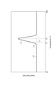
- FIG. 2 is a schematic diagram showing a method for determining the onset temperature and peak temperature of an exothermic peak from a DSC curve.
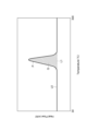
- FIG. 3 is a schematic diagram showing a method for determining the calorific value of an exothermic peak from a DSC curve.
- FIG. 4 is a schematic cross-sectional view showing one embodiment of a dicing/die bonding integrated film.
- FIG. 5 is a schematic cross-sectional view showing one embodiment of a semiconductor device.
- FIG. 6 is a schematic cross-sectional view showing another embodiment of a semiconductor device.
- FIG. 7 is a schematic cross-sectional view showing another embodiment of a semiconductor device.
- a numerical range indicated using “ ⁇ ” indicates a range that includes the numerical values described before and after " ⁇ " as the minimum and maximum values, respectively.
- the upper limit or lower limit described in one numerical range may be replaced with the upper limit or lower limit of another numerical range described in stages.
- the upper limit or lower limit of that numerical range may be replaced with a value shown in an example.
- the upper limit and lower limit values described individually can be arbitrarily combined.
- “A or B" may include either A or B, or may include both.
- the materials exemplified below may be used alone or in combination of two or more types, unless otherwise specified.
- the content of each component in the composition means the total amount of the multiple substances present in the composition, unless otherwise specified.
- (meth)acrylate means acrylate or the corresponding methacrylate.
- Fig. 1 is a schematic cross-sectional view showing one embodiment of a film-like adhesive.
- the film-like adhesive 1 (adhesive film) shown in Fig. 1 may be thermosetting, and may be capable of going through a semi-cured (B stage) state and then becoming fully cured (C stage) after a curing process.
- the film-like adhesive 1 contains a thermosetting resin component (hereinafter sometimes referred to as “component (A)”) and an elastomer (hereinafter sometimes referred to as “component (B)”), and may further contain an inorganic filler (hereinafter sometimes referred to as “component (C)”).
- component (A) may contain, for example, an epoxy resin (hereinafter sometimes referred to as “component (A1)”) and a phenolic resin (hereinafter sometimes referred to as “component (A2)”).
- the film-like adhesive 1 may further contain a coupling agent (hereinafter sometimes referred to as “component (D)”), a curing accelerator (hereinafter sometimes referred to as “component (E)”), other components, etc.
- component (D) a coupling agent
- component (E) a curing accelerator
- the film-like adhesive 1 is a film-like adhesive in which, in a DSC curve obtained by performing differential scanning calorimetry (DSC) under conditions of a heating rate of 10°C/min and a measurement temperature range of 30 to 300°C, the onset temperature of the exothermic peak observed in the DSC curve is 165°C or less, the peak temperature is 185°C or less, and the heat generation amount is 90 J/g or more. Note that there may be multiple exothermic peaks in a DSC curve. In this case, the exothermic peak of interest may be the exothermic peak that exhibits the largest heat generation amount.
- differential scanning calorimetry is performed by heating the sample in an air or nitrogen atmosphere with a sample weight of 10 ⁇ 0.5 mg of film-like adhesive 1, a heating rate of 10°C/min, and a measurement temperature range of 30 to 300°C.
- Conventional film-like adhesives usually have an exothermic peak in the temperature range of 30 to 300°C on the DSC curve. It is presumed that the heat generated in this temperature range is due to the curing reaction of the thermosetting resin component (for example, the reaction between the epoxy resin and the phenolic resin).
- the film-like adhesive of this embodiment has an onset temperature of the exothermic peak of 165°C or less, a peak temperature of 185°C or less, and a heat generation amount of 90 J/g or more. Therefore, even when cured under low temperature and short heating conditions, the storage modulus of the cured product of the film-like adhesive can be improved and the occurrence of chip cracks can be suppressed.
- FIG. 2 is a schematic diagram showing a method for determining the onset temperature and peak temperature of an exothermic peak from a DSC curve.
- the DSC curve shown in FIG. 2 includes a baseline L0 in the temperature range of 30 to 300°C, and an exothermic peak P due to the curing reaction of the film-like adhesive 1, which is observed halfway through the baseline L0.
- the onset temperature is the temperature T1 at the intersection between an extension line L1 of the baseline L0 at the bottom of the exothermic peak P and a tangent line L2 to the DSC curve at the point where the DSC curve shows the maximum gradient at the exothermic peak P.
- the peak temperature is the temperature T2 of the maximum point in the exothermic peak P.
- the onset temperature of the exothermic peak is 165°C or less, and may be, for example, 160°C or 155°C or less. When the onset temperature of the exothermic peak is 165°C or less, it is possible to cure the film-like adhesive under low temperature and short heating conditions.
- the onset temperature of the exothermic peak may be, for example, 100°C or more, 110°C or more, or 120°C or more.
- the peak temperature of the exothermic peak is 185°C or less, and may be, for example, 180°C or less or 175°C or less.
- the peak temperature of the exothermic peak may be, for example, 140°C or more, 150°C or more, or 160°C or more.
- the difference between the peak temperature of the exothermic peak and the onset temperature may be, for example, 45°C or less, 40°C or less, 35°C or less, 30°C or less, 25°C or less, or 20°C or less.
- the difference between the peak temperature of the exothermic peak and the onset temperature is within such a range, the curing reaction of the film-like adhesive tends to proceed sufficiently under low temperature and short heating conditions, making it easier to obtain the desired storage modulus.
- the difference between the peak temperature of the exothermic peak and the onset temperature may be, for example, 5°C or more or 10°C or more.
- the onset temperature and peak temperature of the exothermic peak can be lowered, for example, by increasing the content of component (E) in the film-like adhesive, changing the (E) component to one that acts at a lower temperature, or by increasing the content of component (A) in the film-like adhesive.
- Figure 3 is a schematic diagram showing a method for determining the heat generation amount of an exothermic peak from a DSC curve.
- the DSC curve shown in Figure 3 is similar to the DSC curve shown in Figure 2.
- the heat generation amount Q is calculated by integrating the peak area of the exothermic peak P (the area of the region surrounded by the exothermic peak P and an extension line L1 of the baseline L0).
- the heat value of the exothermic peak is 90 J/g or more, and may be, for example, 95 J/g or more, 100 J/g or more, 105 J/g or more, 110 J/g or more, 115 J/g or more, 120 J/g or more, 125 J/g or more, or 130 J/g or more.
- the heat value of the exothermic peak may be, for example, 250 J/g or less or 200 J/g or less.
- the heat value of the exothermic peak can be improved, for example, by increasing the content of component (A) in the film adhesive, by using a component with a smaller epoxy equivalent as component (A1) of component (A), or by increasing the ratio of the epoxy equivalent of component (A1) to the hydroxyl equivalent of component (A2) (epoxy equivalent of component (A1)/hydroxyl equivalent of component (A2)).
- the components that make up the film-like adhesive of this embodiment are described below. By using the components shown below, it tends to be easier to produce a film-like adhesive that satisfies the above-mentioned conditions for the onset temperature, peak temperature, and amount of heat generation of the heat generation peak.
- (A) component thermosetting resin component
- (A1) component epoxy resin
- the (A1) component can be used without any particular limitation as long as it has an epoxy group in the molecule.
- (A1) component includes, for example, bisphenol A type epoxy resin; bisphenol F type epoxy resin; bisphenol S type epoxy resin; phenol novolac type epoxy resin; cresol novolac type epoxy resin; bisphenol A novolac type epoxy resin; bisphenol F novolac type epoxy resin; stilbene type epoxy resin; triazine skeleton-containing epoxy resin; fluorene skeleton-containing epoxy resin; triphenol methane type epoxy resin; biphenyl type epoxy resin; xylylene type epoxy resin; biphenyl aralkyl type epoxy resin; naphthalene type epoxy resin; polyfunctional phenols, diglycidyl ether compounds of polycyclic aromatics such as anthracene, etc.
- the (A1) component may contain cresol novolac type epoxy resin, bisphenol F type epoxy resin, or bisphenol A type epoxy resin from the viewpoint of film tackiness, flexibility, etc.
- Bisphenol F type epoxy resins have a relatively low softening point, and many of them have a softening point of 40° C. or lower.
- the (A1) component may contain an epoxy resin having a softening point of 40°C or lower (or an epoxy resin that is liquid at 30°C, hereinafter sometimes referred to as "(A1a) component”).
- the (A1) component may be a combination of the (A1a) component and an epoxy resin having a softening point of more than 40°C (or an epoxy resin that is solid at 30°C, hereinafter sometimes referred to as "(A1b) component”).
- the (A1) component contains the (A1a) component, it tends to be easier to improve the storage modulus after curing.
- the (A1) component is a combination of the (A1a) component and the (A1b) component, it tends to be easier to achieve a thin film.
- the softening point refers to the value measured by the ring and ball method in accordance with JIS K7234:1986.
- component (A1a) Commercially available products of component (A1a) include, for example, EXA-830CRP (product name, manufactured by DIC Corporation, liquid at 30°C), YDF-8170C (product name, manufactured by Nippon Steel Chemical & Material Co., Ltd., liquid at 30°C), and EP-4088S (product name, manufactured by ADEKA Corporation, liquid at 30°C).
- EXA-830CRP product name, manufactured by DIC Corporation, liquid at 30°C
- YDF-8170C product name, manufactured by Nippon Steel Chemical & Material Co., Ltd., liquid at 30°C
- EP-4088S product name, manufactured by ADEKA Corporation, liquid at 30°C
- the content of the (A1a) component may be 5 mass% or more, 10 mass% or more, or 15 mass% or more, and 80 mass% or less, 70 mass% or less, or 65 mass% or less, based on the total amount of the (A1) component.
- the content of the (A1a) component in the (A1) component in the adhesive composition when forming the film-like adhesive may be in the same range as above.
- the content of the (A1b) component may be 20% by mass or more, 30% by mass or more, or 35% by mass or more, and 95% by mass or less, 90% by mass or less, or 85% by mass or less, based on the total amount of the (A1) component.
- the content of the (A1b) component in the (A1) component in the adhesive composition when forming the film-like adhesive may be in the same range as above.
- the epoxy equivalent of component (A1) is not particularly limited, but may be 90 to 300 g/eq or 110 to 290 g/eq. When the epoxy equivalent of component (A1) is in such a range, it tends to be easier to ensure the fluidity of the adhesive composition when forming the film-like adhesive while maintaining the bulk strength of the film-like adhesive.
- Component (A2) Phenol resin Component (A2) is a component that acts as a curing agent for component (A1), i.e., it can be a curing agent for epoxy resin. By including component (A2) in the film-like adhesive, the film-like adhesive can be highly crosslinked, improving the storage modulus after curing.
- the (A2) component can be used without any particular restriction as long as it has a phenolic hydroxyl group in the molecule.
- the (A2) component is not particularly limited as long as it has a phenolic hydroxyl group in the molecule.
- Examples of the (A2) component include novolac-type phenolic resins obtained by condensing or co-condensing phenols such as phenol, cresol, resorcin, catechol, bisphenol A, bisphenol F, phenylphenol, aminophenol, etc. and/or naphthols such as ⁇ -naphthol, ⁇ -naphthol, dihydroxynaphthalene, etc.
- the phenolic resin may include a novolac type phenolic resin or a phenylaralkyl type phenolic resin.
- the hydroxyl equivalent of component (A2) may be 70 g/eq or more, or 70 to 300 g/eq. If the hydroxyl equivalent of component (A2) is 70 g/eq or more, the storage modulus tends to be improved, and if it is 300 g/eq or less, it becomes possible to prevent defects due to the generation of foaming, outgassing, etc.
- the softening point of the (A2) component is not particularly limited, but may be, for example, 90°C or higher, 100°C or higher, or 110°C or higher.
- the upper limit of the softening point of the (A2) component may be, for example, 200°C or lower.
- component (A2) Commercially available products of component (A2) include, for example, PSM-4326 (trade name, manufactured by Gun-ei Chemical Industry Co., Ltd., softening point: 120°C), J-DPP-140 (trade name, manufactured by JFE Chemical Corporation, softening point: 140°C), and GPH-103 (trade name, manufactured by Nippon Kayaku Co., Ltd., softening point: 99-106°C).
- the ratio of the epoxy equivalent of component (A1) to the hydroxyl equivalent of component (A2) may be 0.30/0.70 to 0.70/0.30, 0.35/0.65 to 0.65/0.35, 0.40/0.60 to 0.60/0.40, or 0.45/0.55 to 0.55/0.45, from the viewpoint of curability. If the equivalent ratio is 0.30/0.70 or more, more sufficient curability tends to be obtained. If the equivalent ratio is 0.70/0.30 or less, it is possible to prevent the viscosity from becoming too high, and more sufficient fluidity can be obtained.
- the content of the (A1) component (the sum of the (A1a) component and the (A1b) component) may be 20% by mass or more, 22% by mass or more, 25% by mass or more, 28% by mass or more, 30% by mass or more, 32% by mass or more, 35% by mass or more, 38% by mass or more, or 40% by mass or more, based on the total amount of the film-like adhesive.
- the content of the (A1) component may be 50% by mass or less, 48% by mass or less, or 45% by mass or less, based on the total amount of the film-like adhesive.
- the content of the (A1) component (the sum of the (A1a) component and the (A1b) component) in the adhesive composition when forming the film-like adhesive may be the same as the above range.
- the content of the (A2) component may be 10% by mass or more, 12% by mass or more, 15% by mass or more, 18% by mass or more, 20% by mass or more, 22% by mass or more, or 25% by mass or more, based on the total amount of the film-like adhesive.
- the content of the (A2) component may be 35% by mass or less, 32% by mass or less, or 30% by mass or less, based on the total amount of the film-like adhesive.
- the content of the (A2) component in the adhesive composition when forming the film-like adhesive may be the same as the above range.
- the content of the (A) component (the sum of the (A1) component and the (A2) component) may be 35% by mass or more, 38% by mass or more, 40% by mass or more, 42% by mass or more, 45% by mass or more, 48% by mass or more, 50% by mass or more, 52% by mass or more, 55% by mass or more, 58% by mass or more, 60% by mass or more, 62% by mass or more, or 65% by mass or more, based on the total amount of the film-like adhesive.
- the content of the (A) component is in such a range, the storage modulus after curing tends to be more easily improved.
- the content of the (A) component may be 80% by mass or less, 75% by mass or less, or 70% by mass or less, based on the total amount of the film-like adhesive.
- the content of the (A) component (the sum of the (A1) component and the (A2) component) in the adhesive composition when forming the film-like adhesive may be the same as the above range.
- (B) component elastomer
- the (B) component include acrylic resin, polyester resin, polyamide resin, polyimide resin, silicone resin, butadiene resin, and modified products of these resins.
- the (B) component include polymers having organopolysiloxane in the side chain.
- the (B) component may be an acrylic resin (acrylic rubber) having a structural unit derived from a (meth)acrylic acid ester as a main component, since it has less ionic impurities and is more excellent in heat resistance, is easier to ensure the connection reliability of the semiconductor device, and is more excellent in fluidity.
- the glass transition temperature (Tg) of the (B) component may be 0 to 30°C. If the Tg of the (B) component is 0°C or higher, the adhesive strength of the film-like adhesive can be improved, and the flexibility of the film-like adhesive tends to be prevented from becoming too high. If the Tg of the (B) component is 30°C or lower, the film-like adhesive tends to be prevented from decreasing in flexibility, and the adhesive tends to have excellent breaking strength and excellent processability when a thin film is formed.
- the glass transition temperature (Tg) of the (B) component may be 5°C or higher or 10°C or higher, and may be 25°C or lower or 20°C or lower.
- Tg means a value measured using a DSC (differential scanning calorimeter) (for example, Thermo Plus 2, manufactured by Rigaku Corporation).
- the Tg of the (B) component can be adjusted to a desired range by adjusting the type and content of the constituent units constituting the (B) component (when the (B) component is an acrylic resin (acrylic rubber), the constituent units derived from (meth)acrylic acid esters).
- the weight average molecular weight (Mw) of component (B) may be 100,000 or more, 300,000 or more, or 500,000 or more, and may be 3,000,000 or less, 2,000,000 or less, or 1,000,000 or less.
- Mw means a value measured by gel permeation chromatography (GPC) and converted using a calibration curve of standard polystyrene. Note that, when multiple peaks are observed in GPC, the weight average molecular weight resulting from the peak with the highest peak intensity is defined as the weight average molecular weight in this specification.
- component (B) Commercially available products of component (B) include SG-P3 and SG-80H (both manufactured by Nagase ChemteX Corporation) and KH-CT-865 (manufactured by Resonac Corporation).
- the content of the (B) component may be 15% by mass or more, 20% by mass or more, or 25% by mass or more based on the total amount of the film-like adhesive.
- the content of the (B) component is in this range, the thin film is excellent in formability, has excellent breaking strength when a thin film is formed, and tends to suppress warping of the semiconductor device (semiconductor package).
- the content of the (B) component may be 45% by mass or less, 40% by mass or less, or 35% by mass or less based on the total amount of the film-like adhesive.
- the content of the (B) component in this range the storage modulus after curing tends to be further improved.
- the content of the (B) component in the adhesive composition when forming the film-like adhesive may be the same as the above range.
- Component (C) Inorganic Filler
- the film-like adhesive 1 may further contain component (C). That is, the film-like adhesive 1 may exist in an embodiment that contains component (C) and an embodiment that substantially does not contain component (C).
- component (C) examples include aluminum hydroxide, magnesium hydroxide, calcium carbonate, magnesium carbonate, calcium silicate, magnesium silicate, calcium oxide, magnesium oxide, aluminum oxide, aluminum nitride, aluminum borate whiskers, boron nitride, and silica.
- component (C) may be silica from the viewpoint of adjusting the melt viscosity.
- the shape of component (C) is not particularly limited, but may be spherical.
- the average particle size of the (C) component may be 0.7 ⁇ m or less, 0.6 ⁇ m or less, 0.5 ⁇ m or less, 0.4 ⁇ m or less, or 0.3 ⁇ m or less.
- the average particle size of the (C) component may be, for example, 0.01 ⁇ m or more.
- the average particle size means the particle size with an accumulated frequency of 50% in the particle size distribution determined by the laser diffraction/scattering method.
- the average particle size of the (C) component can also be determined by using a film-like adhesive containing the (C) component.
- the film-like adhesive is heated to decompose the resin component, and the residue obtained is dispersed in a solvent to prepare a dispersion, and the average particle size of the (C) component can be determined from the particle size distribution obtained by applying the laser diffraction/scattering method to the dispersion.
- the content of the (C) component may be 0 to 25% by mass based on the total amount of the film-like adhesive.
- the content of the (C) component is in this range, it tends to be possible to further reduce the thickness.
- the thin film formed has excellent breaking strength and excellent processability, and warping of the semiconductor device (semiconductor package) tends to be suppressed.
- the content of the (C) component may be 22% by mass or less, 20% by mass or less, 17% by mass or less, 15% by mass or less, 12% by mass or less, 10% by mass or less, 7% by mass or less, 5% by mass or less, 4% by mass or less, 3% by mass or less, 2% by mass or less, 1% by mass or less, 0.5% by mass or less, or 0.1% by mass or less based on the total amount of the film-like adhesive.
- the content of the (C) component may be 0% by mass based on the total amount of the film-like adhesive. That is, in one embodiment, the film-like adhesive does not need to contain the (C) component.
- the content of component (C) may be 0% by mass or more, more than 0% by mass, 1% by mass or more, 3% by mass or more, or 5% by mass or more based on the total amount of the film-like adhesive.
- the content of component (C) in the adhesive composition when forming the film-like adhesive may be in the same range as above.
- the (A) component and the (B) component, or the (A), (B), and (C) components may be the main components of the film-like adhesive of this embodiment.
- the total content of the (A) component and the (B) component, or the total content of the (A), (B), and (C) components may be, for example, 70% by mass or more, 80% by mass or more, 90% by mass or more, 95% by mass or more, 96% by mass or more, 97% by mass or more, 98% by mass or more, 99% by mass or more, 99.5% by mass or more, 99.7% by mass or more, or 99.9% by mass or more.
- the total content of the (A) component and the (B) component, or the total content of the (A), (B), and (C) components may be, for example, 100% by mass or less, 99.9% by mass or less, 99.7% by mass or less, or 99.5% by mass or less.
- Component (D) Coupling Agent
- Component (D) may be a silane coupling agent.
- the silane coupling agent include ⁇ -ureidopropyltriethoxysilane, ⁇ -mercaptopropyltrimethoxysilane, 3-phenylaminopropyltrimethoxysilane, and 3-(2-aminoethyl)aminopropyltrimethoxysilane.
- Component (E) Curing Accelerator
- the component (E) include imidazoles and derivatives thereof, organic phosphorus compounds, secondary amines, tertiary amines, quaternary ammonium salts, etc.
- the component (E) may be imidazoles and derivatives thereof.
- imidazoles examples include 2-methylimidazole, 1-benzyl-2-methylimidazole, 2-phenylimidazole, 1-cyanoethyl-2-phenylimidazole, and 1-cyanoethyl-2-methylimidazole.
- Component (E) may contain 2-phenylimidazole, which helps promote curing at low temperatures.
- the film adhesive may further contain other components.
- other components include pigments, ion scavengers, antioxidants, etc.
- the total content of the (D) component, the (E) component, and other components may be 0 mass% or more, 0.1 mass% or more, 0.3 mass% or more, or 0.5 mass% or more based on the total amount of the film-like adhesive, and may be 30 mass% or less, 20 mass% or less, 10 mass% or less, 5 mass% or less, 4 mass% or less, 3 mass% or less, 2 mass% or less, or 1 mass% or less.
- the total content of the (D) component, the (E) component, and other components in the adhesive composition when forming the film-like adhesive may be in the same range as above.
- the thickness of the film-like adhesive 1 may be 1 to 15 ⁇ m.
- the thickness of the film-like adhesive 1 may be 12 ⁇ m or less, 10 ⁇ m or less, 8 ⁇ m or less, or 7 ⁇ m or less.
- the thickness of the film-like adhesive 1 can be determined, for example, by measuring the thickness at five points on a cross-section of the film-like adhesive 1 using a scanning microscope photograph and calculating the average of the measured values.
- the storage modulus of the cured product at 150°C may be 50 MPa or more, 55 MPa or more, 60 MPa or more, 65 MPa or more, 70 MPa or more, 75 MPa or more, 80 MPa or more, 85 MPa or more, 90 MPa or more, 95 MPa or more, 100 MPa or more, 105 MPa or more, 110 MPa or more, 115 MPa or more, 120 MPa or more, 125 MPa or more, 130 MPa or more, 135 MPa or more, 140 MPa or more, 145 MPa or more, or 150 MPa or more.
- the storage modulus is 50 MPa or more, it is possible to cover the brittleness of the semiconductor chip due to the thin film, and as a result, it is possible to suppress the occurrence of chip cracks.
- the upper limit of the storage modulus is not particularly limited, but may be, for example, 500 MPa or less, 300 MPa or less, 250 MPa or less, or 200 MPa or less.
- the storage modulus at 150°C of the cured product when the film-like adhesive is cured under conditions of 140°C and 30 minutes can be measured, for example, by the following method.
- a sample for measurement is prepared by laminating multiple 5 ⁇ m-thick film-like adhesives to a thickness of 20 ⁇ m or more and cutting this into a size of 4 mm wide x 20 mm long or more.
- the prepared sample is cured under conditions of 140°C and 30 minutes, and then the cured sample is set in a dynamic viscoelasticity measuring device (Rheogel E-4000, manufactured by UBM Co., Ltd.) and dynamic viscoelasticity is measured in a temperature dependence measurement mode in which a tensile load is applied and measurements are made from room temperature (25°C) to 300°C under conditions of a chuck distance of 20 mm, a frequency of 10 Hz, and a heating rate of 3°C/min. The value of the storage modulus at 150°C is then read, and this value is regarded as the storage modulus at 150°C.
- a dynamic viscoelasticity measuring device Heogel E-4000, manufactured by UBM Co., Ltd.
- the film-like adhesive 1 (adhesive film) shown in FIG. 1 is formed by forming an adhesive composition containing components (A) and (B), and, if necessary, component (C) and added components, into a film.
- a film-like adhesive 1 can be formed by applying the adhesive composition to a support film.
- a varnish (adhesive varnish) containing the adhesive composition and a solvent may be used.
- the adhesive varnish is prepared by mixing or kneading components (A) and (B), and, if necessary, component (C) and added components in a solvent, and the obtained adhesive varnish is applied to a support film, and the solvent is removed by heating and drying to obtain the film-like adhesive 1.
- the support film is not particularly limited as long as it can withstand the above-mentioned heat drying, but may be, for example, a polyester film, a polypropylene film, a polyethylene terephthalate film, a polyimide film, a polyetherimide film, a polyethylene naphthalate film, a polymethylpentene film, or the like.
- the support film may be a multi-layer film combining two or more types, and may have a surface treated with a silicone-based, silica-based, or other release agent.
- the thickness of the support film may be, for example, 10 to 200 ⁇ m or 20 to 170 ⁇ m.
- Mixing or kneading can be carried out using a conventional mixer, a mixing machine, a triple roll mill, a ball mill, or other dispersing machine, in any suitable combination.
- the solvent used in preparing the adhesive varnish is not limited as long as it can dissolve, knead, or disperse each component uniformly, and any conventionally known solvent can be used.
- solvents include ketone solvents such as acetone, methyl ethyl ketone, methyl isobutyl ketone, and cyclohexanone, as well as dimethylformamide, dimethylacetamide, N-methylpyrrolidone, toluene, and xylene. From the standpoint of drying speed and cost, the solvent may be methyl ethyl ketone or cyclohexanone.
- any known method can be used to apply the adhesive varnish to the support film, such as knife coating, roll coating, spray coating, gravure coating, bar coating, curtain coating, etc.
- the heat drying conditions there are no particular restrictions on the heat drying conditions as long as the solvent used is sufficiently evaporated, but the conditions may be 50 to 150°C and 1 to 30 minutes.
- the film-like adhesive 1 can be thinned, it can be suitably used in the manufacturing process of a semiconductor device in which multiple semiconductor chips are stacked.
- the semiconductor device may be a stacked MCP or a three-dimensional NAND memory.
- FIG. 4 is a schematic cross-sectional view showing one embodiment of a dicing/die bonding integrated film.
- the dicing/die bonding integrated film 10 shown in Fig. 4 includes a base layer 2, a pressure-sensitive adhesive layer 3, and an adhesive layer 1A made of the above-mentioned film-like adhesive 1, in this order.
- the base layer 2 and the pressure-sensitive adhesive layer 3 can be a dicing film 4.
- the lamination process to the semiconductor wafer is performed only once, so that the efficiency of the work can be improved.
- the dicing/die bonding integrated film may be in the form of a film, a sheet, a tape, or the like.
- the dicing film 4 comprises a base layer 2 and an adhesive layer 3 provided on the base layer 2.
- the substrate layer 2 examples include plastic films such as polytetrafluoroethylene film, polyethylene terephthalate film, polyethylene film, polypropylene film, polymethylpentene film, and polyimide film. These substrate layers 2 may be subjected to surface treatments such as primer coating, UV treatment, corona discharge treatment, polishing treatment, and etching treatment, as necessary.
- the adhesive layer 3 is a layer made of an adhesive.
- the adhesive may be either a radiation-curable or non-radiation-curable adhesive.
- the radiation may be, for example, ultraviolet light.
- a non-radiation-curable adhesive is an adhesive that exhibits a certain level of adhesiveness when pressure is applied for a short period of time.
- a radiation-curable adhesive is an adhesive that has the property of decreasing adhesiveness when exposed to radiation (for example, ultraviolet light).
- the thickness of the dicing film 4 may be 60 to 150 ⁇ m or 70 to 130 ⁇ m from the standpoint of economy and ease of handling of the film.
- the dicing/die bonding integrated film 10 can be obtained, for example, by preparing a film-like adhesive 1 and a dicing film 4, and bonding the film-like adhesive 1 to the pressure-sensitive adhesive layer 3 of the dicing film 4.
- the dicing/die bonding integrated film 10 can also be obtained, for example, by preparing a dicing film 4, and applying an adhesive composition (adhesive varnish) onto the pressure-sensitive adhesive layer 3 of the dicing film 4 in the same manner as in the method of forming the film-like adhesive 1 described above.
- the film-like adhesive and the integrated dicing and die bonding film may be used in a manufacturing process for a semiconductor device, or may be used in a manufacturing process for a semiconductor device in which multiple semiconductor chips are stacked.
- the film-like adhesive and the integrated dicing and die bonding film may be used in a manufacturing process for a semiconductor device that includes a process of bonding an adhesive layer of the film-like adhesive or the integrated dicing and die bonding film to a semiconductor wafer or an already-singulated semiconductor chip, and obtaining a semiconductor chip with an adhesive piece by cutting with a rotary blade, laser, or stretching, and a process of adhering the semiconductor chip with the adhesive piece onto a support member or another semiconductor chip via the adhesive piece.
- the film-like adhesive is also suitable for use as an adhesive for bonding semiconductor chips together in stacked MCPs (e.g., three-dimensional NAND memory), which are semiconductor devices made by stacking multiple semiconductor chips.
- stacked MCPs e.g., three-dimensional NAND memory
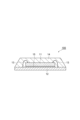
- FIG. 5 is a schematic cross-sectional view showing one embodiment of a semiconductor device.
- the semiconductor device 100 shown in Fig. 5 includes a semiconductor chip 11 (first semiconductor chip), a support member 12 on which the semiconductor chip 11 is mounted, and an adhesive member 15.
- the adhesive member 15 is provided between the semiconductor chip 11 and the support member 12, and bonds the semiconductor chip 11 and the support member 12.
- the adhesive member 15 is a cured product of an adhesive composition (cured product of a film-like adhesive).
- the connection terminals (not shown) of the semiconductor chip 11 are electrically connected to external connection terminals (not shown) via bonding wires 13, and are sealed with a sealing material 14.
- FIG. 6 is a schematic cross-sectional view showing another embodiment of a semiconductor device.
- the first-stage semiconductor chip 11a first semiconductor chip
- the second-stage semiconductor chip 11b second semiconductor chip
- the connection terminals (not shown) of the first-stage semiconductor chip 11a and the second-stage semiconductor chip 11b are electrically connected to external connection terminals via bonding wires 13 and sealed with a sealing material 14.
- the semiconductor device 110 shown in FIG. 6 can be said to further include another semiconductor chip (11b) stacked on the surface of the semiconductor chip (11a) in the semiconductor device 100 shown in FIG. 5.
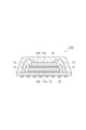
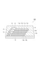
- the semiconductor device 120 shown in FIG. 7 includes a support member 12 and semiconductor chips 11a (first semiconductor chip), 11b (second semiconductor chip), 11c (third semiconductor chip), and 11d (fourth semiconductor chip) stacked on the support member 12.
- the four semiconductor chips 11a, 11b, 11c, and 11d are stacked at positions shifted from each other in the horizontal direction (direction perpendicular to the stacking direction) for connection with a connection terminal (not shown) formed on the surface of the support member 12 (see FIG. 7).
- FIG. 7 illustrates a semiconductor device in which four semiconductor chips are stacked, but the number of stacked semiconductor chips is not limited to this.
- FIG. 7 illustrates a semiconductor device in which the semiconductor chips are stacked in positions shifted from each other in the horizontal direction (direction perpendicular to the stacking direction), but the semiconductor device may be one in which the semiconductor chips are stacked in positions that are not shifted from each other in the horizontal direction (direction perpendicular to the stacking direction).
- the semiconductor device (semiconductor package) shown in Figures 5, 6, and 7 can be obtained by a method including a step of interposing the above-mentioned film-like adhesive between a semiconductor chip (first semiconductor chip) and a support member, or between a semiconductor chip (first semiconductor chip) and a semiconductor chip (second semiconductor chip), and bonding the semiconductor chip (first semiconductor chip) and the support member, or between a semiconductor chip (first semiconductor chip) and a semiconductor chip (second semiconductor chip).
- the above-mentioned film-like adhesive is interposed between a semiconductor chip and a support member, or between a semiconductor chip (first semiconductor chip) and a semiconductor chip (second semiconductor chip), and these are heated and pressed to bond the two together, and then, as necessary, a heat curing step, a wire bonding step, a sealing step using a sealing material, a heating and melting step including reflow using solder, and the like can be obtained.
- the semiconductor device can be obtained, for example, by a method comprising a step of attaching a semiconductor wafer to the adhesive layer of the above-mentioned dicing/die bonding integrated film (lamination step), a step of cutting the semiconductor wafer with the adhesive layer attached to produce a plurality of individual adhesive piece-attached semiconductor chips (dicing step), and a step of adhering a first adhesive piece-attached semiconductor chip having a first semiconductor chip and a first adhesive piece to a support member via the first adhesive piece as the adhesive piece-attached semiconductor chip (step of adhering the adhesive piece-attached semiconductor chip to a support member via an adhesive piece) (first adhering step).
- the method for manufacturing a semiconductor device may further include a step of adhering a second semiconductor chip with adhesive piece, which has a second semiconductor chip and a second adhesive piece, to the surface of the first semiconductor chip in the first semiconductor chip with adhesive piece adhered to the support member via the second adhesive piece (a step of adhering another semiconductor chip with adhesive piece to the surface of the semiconductor chip adhered to the support member via an adhesive piece possessed by the other semiconductor chip with adhesive piece) (second adhering step).
- the lamination process is a process in which a semiconductor wafer is pressed against the adhesive layer 1A of the dicing/die bonding integrated film 10, and the semiconductor wafer is adhered and held in place. This process may be performed while pressing with a pressing means such as a pressing roll.
- Semiconductor wafers include, for example, single crystal silicon, polycrystalline silicon, various ceramics, and compound semiconductors such as gallium arsenide.
- the dicing process is a process in which a semiconductor wafer is diced. This allows the semiconductor wafer to be cut to a predetermined size, producing a number of individual semiconductor chips with adhesive pieces attached. Dicing can be performed, for example, from the circuit side of the semiconductor wafer in a conventional manner.
- This process can employ, for example, a method known as full cut, in which a cut is made all the way to the dicing film, a method in which a half cut is made in the semiconductor wafer and the wafer is divided by cooling and pulling, or a method in which the wafer is divided by a laser.
- a method known as full cut in which a cut is made all the way to the dicing film
- a method in which a half cut is made in the semiconductor wafer and the wafer is divided by cooling and pulling
- a method in which the wafer is divided by a laser There are no particular limitations on the dicing device used in this process, and any conventionally known device can be used.
- Semiconductor chips are composed of, for example, a circuit layer and a semiconductor layer (for example, single crystal silicon, polycrystalline silicon, various ceramics, compound semiconductors such as gallium arsenide, etc.).
- semiconductor chips include ICs (integrated circuits).
- support members include lead frames such as 42 alloy lead frames and copper lead frames; plastic films such as polyimide resin and epoxy resin; modified plastic films in which a substrate such as glass nonwoven fabric is impregnated and hardened with plastics such as polyimide resin and epoxy resin; and ceramics such as alumina.
- the method for manufacturing a semiconductor device may include a pick-up step as necessary.
- the pick-up step is a step of picking up the semiconductor chips with adhesive pieces in order to peel off the semiconductor chips with adhesive pieces that have been adhesively fixed to the dicing/die bonding integrated film.
- the pick-up method is not particularly limited, and various conventionally known methods can be used.
- such a method includes a method in which each semiconductor chip with adhesive pieces is pushed up from the dicing/die bonding integrated film side by a needle, and the pushed-up semiconductor chips with adhesive pieces are picked up by a pick-up device.
- the adhesive layer is of a radiation (e.g., ultraviolet) curing type
- pick-up can be performed after irradiating the adhesive layer with radiation. This reduces the adhesive strength of the adhesive layer to the adhesive piece, making it easier to peel off the semiconductor chip with the adhesive piece attached. As a result, pick-up is possible without damaging the semiconductor chip with the adhesive piece attached.
- a radiation e.g., ultraviolet
- the first bonding step is a step of bonding a semiconductor chip with a first adhesive piece formed by dicing to a support member for mounting the semiconductor chip via the first adhesive piece.
- the manufacturing method of a semiconductor device may include a step (second bonding step) of bonding a semiconductor chip with a second adhesive piece to the surface of the semiconductor chip bonded to the support member via the second adhesive piece, as necessary. Both bonding steps can be performed by pressure bonding. There are no particular limitations on the pressure bonding conditions, and they can be set appropriately as necessary.
- the pressure bonding conditions may be, for example, a temperature of 80 to 160°C, a load of 5 to 15 N, and a time of 1 to 10 seconds.
- the support member can be, for example, the same support member as above.
- the method for manufacturing a semiconductor device may include a step of further thermally curing the adhesive pieces (the first adhesive piece in the semiconductor chip with the first adhesive piece, and the second adhesive piece in the semiconductor chip with the second adhesive piece) or the film-like adhesive (thermal curing step) as necessary.
- the adhesive pieces the first adhesive piece in the semiconductor chip with the first adhesive piece, and the second adhesive piece in the semiconductor chip with the second adhesive piece
- pressure may be applied at the same time to harden them.
- the heating temperature in this step can be appropriately changed depending on the constituent components of the adhesive pieces.
- the heating temperature may be, for example, 60 to 200°C or 100 to 180°C.
- the temperature or pressure may be changed stepwise.
- the heating time may be, for example, 1 to 120 minutes or 15 to 60 minutes.
- the method for manufacturing a semiconductor device may include, as necessary, a step of electrically connecting the first and second semiconductor chips to the support member with bonding wires, more specifically, a step of electrically connecting the electrode pads on the semiconductor chips to the tips of the terminal portions (inner leads) of the support member with bonding wires (wire bonding step).
- wire bonding step For example, gold wire, aluminum wire, copper wire, etc., are used as the bonding wire.
- the temperature during wire bonding may be within a range of 80 to 250°C or 80 to 220°C. The heating time may be several seconds to several minutes.
- Wire bonding may be performed by combining ultrasonic vibration energy and compression energy by applied pressure while heated within the above temperature range.
- the manufacturing method of a semiconductor device may include a step of sealing the semiconductor chip with a sealing material (sealing step) as necessary. This step is performed to protect the semiconductor chip or bonding wires mounted on the support member. This step can be performed by molding the sealing resin (sealing resin) in a mold.
- the sealing resin may be, for example, an epoxy-based resin. The support member and residue are embedded by the heat and pressure during sealing, and peeling due to air bubbles at the adhesive interface can be prevented.
- the method for manufacturing a semiconductor device may, if necessary, include a process (post-curing process) for completely curing any encapsulating resin that is not fully cured in the encapsulating process. Even if the adhesive pieces are not thermally cured in the encapsulating process, in this process, the adhesive pieces are thermally cured together with the encapsulating resin, making it possible to bond and fix the pieces.
- the heating temperature in this process can be set appropriately depending on the type of encapsulating resin, and may be within the range of 165 to 185°C, for example, and the heating time may be approximately 0.5 to 8 hours.
- the method for manufacturing a semiconductor device may, as necessary, include a step of heating the semiconductor chip attached to the support member or the semiconductor chip using a reflow furnace (heating and melting step).
- the resin-encapsulated semiconductor device may be surface-mounted on the support member.
- surface mounting methods include reflow soldering, in which solder is first supplied onto a printed wiring board, then heated and melted by hot air or the like, and soldered.
- heating methods include hot air reflow and infrared reflow.
- the heating method may be one that heats the entire surface or one that heats localized areas.
- the heating temperature may be, for example, within the range of 240 to 280°C.
- Component (A2) Phenolic resin (A2-1) PSM-4326 (trade name, manufactured by Gun-ei Chemical Industry Co., Ltd., novolac type phenolic resin, hydroxyl equivalent: 105 g/eq, softening point: 120° C.)
- A2-2 MEH-7800M (product name, manufactured by Meiwa Chemical Industry Co., Ltd., phenol novolac type phenolic resin, hydroxyl equivalent: 175 g/eq, softening point: 61 to 90° C.)
- Component (D) Coupling agent (D-1) Z-6119 (trade name, manufactured by Dow Toray Co., Ltd., ⁇ -ureidopropyltriethoxysilane) (D-2) A-189 (trade name, manufactured by Nippon Unicar Co., Ltd., ⁇ -mercaptopropyltrimethoxysilane)
- Component (E) Curing accelerator (E-1) 2PZ-T (trade name, manufactured by Shikoku Chemical Industry Co., Ltd., 2-phenylimidazole) (E-2) 2PZ-CN (trade name, manufactured by Shikoku Chemical Industry Co., Ltd., 1-cyanoethyl-2-phenylimidazole)
- the baseline of the analysis temperature range was specified and the peak area was integrated to calculate the amount of heat generated (unit: J/g).
- a total area analysis method was used as a means of analyzing the onset temperature, and by instructing analysis in the temperature range of 30°C to 300°C, the intersection point between the baseline of the heat generation peak in each DSC curve and the maximum slope point was calculated, and the onset temperature (unit: °C) was obtained.
- the onset temperature was analyzed by determining the maximum point of the exothermic peak and calculating the peak temperature (unit: ° C.). The results are shown in Table 1.
- the storage modulus after curing was measured using the film-like adhesives of Examples 1 to 4 and Comparative Examples 1 and 2.
- the storage modulus after curing was measured by the following method. That is, a plurality of 5 ⁇ m thick film-like adhesives were laminated to a thickness of 20 ⁇ m or more, and this was made into a size of 4 mm wide x 20 mm long or more to prepare a sample for measurement. The prepared sample was cured under conditions of 140° C.
- the cured sample (cured product) was set in a dynamic viscoelasticity measuring device (Rheogel E-4000, manufactured by UBM Co., Ltd.) and dynamic viscoelasticity was measured in a temperature dependency measurement mode in which a tensile load was applied and measurements were made from room temperature (25° C.) to 300° C. under conditions of a chuck distance of 20 mm, a frequency of 10 Hz, and a temperature rise rate of 3° C./min.
- the value of the storage modulus at 150° C. was read, and this value was taken as the storage modulus at 150° C.
- Table 1 The larger the storage modulus at 150° C. (for example, 50 MPa or more), the more the fragility of the semiconductor chip due to the thinning can be compensated for, and as a result, the occurrence of chip cracks can be suppressed.
- Table 1 The results are shown in Table 1.
- 1...film-like adhesive 1A...adhesive layer, 2...base material layer, 3...adhesive layer, 4...dicing film, 10...dicing and die bonding integrated film, 11, 11a, 11b, 11c, 11d...semiconductor chip, 12...support member, 13...bonding wire, 14...sealant, 15, 15a, 15b, 15c, 15d...adhesive member, 16...terminal, 100, 110, 120...semiconductor device.
Landscapes
- Engineering & Computer Science (AREA)
- Microelectronics & Electronic Packaging (AREA)
- Chemical & Material Sciences (AREA)
- Power Engineering (AREA)
- Organic Chemistry (AREA)
- Computer Hardware Design (AREA)
- Physics & Mathematics (AREA)
- Condensed Matter Physics & Semiconductors (AREA)
- General Physics & Mathematics (AREA)
- Polymers & Plastics (AREA)
- Medicinal Chemistry (AREA)
- Chemical Kinetics & Catalysis (AREA)
- Manufacturing & Machinery (AREA)
- Health & Medical Sciences (AREA)
- Inorganic Chemistry (AREA)
- Adhesives Or Adhesive Processes (AREA)
- Adhesive Tapes (AREA)
- Die Bonding (AREA)
Priority Applications (4)
| Application Number | Priority Date | Filing Date | Title |
|---|---|---|---|
| CN202480002344.8A CN119110836A (zh) | 2023-03-15 | 2024-03-14 | 膜状黏合剂、切割晶粒接合一体型膜、以及半导体装置及其制造方法 |
| KR1020257032323A KR20250159195A (ko) | 2023-03-15 | 2024-03-14 | 필름상 접착제, 다이싱·다이본딩 일체형 필름, 및 반도체 장치 및 그 제조 방법 |
| JP2025507156A JPWO2024190881A1 (enExample) | 2023-03-15 | 2024-03-14 | |
| US18/860,697 US20250293077A1 (en) | 2023-03-15 | 2024-03-14 | Film adhesive, dicing and die-bonding integral film, semiconductor device, and manufacturing method for same |
Applications Claiming Priority (4)
| Application Number | Priority Date | Filing Date | Title |
|---|---|---|---|
| JPPCT/JP2023/010166 | 2023-03-15 | ||
| PCT/JP2023/010166 WO2024189855A1 (ja) | 2023-03-15 | 2023-03-15 | フィルム状接着剤、ダイシング・ダイボンディング一体型フィルム、並びに半導体装置及びその製造方法 |
| JPPCT/JP2023/029152 | 2023-08-09 | ||
| PCT/JP2023/029152 WO2025032779A1 (ja) | 2023-08-09 | 2023-08-09 | フィルム状接着剤、ダイシング・ダイボンディング一体型フィルム、並びに半導体装置及びその製造方法 |
Publications (1)
| Publication Number | Publication Date |
|---|---|
| WO2024190881A1 true WO2024190881A1 (ja) | 2024-09-19 |
Family
ID=92755409
Family Applications (1)
| Application Number | Title | Priority Date | Filing Date |
|---|---|---|---|
| PCT/JP2024/010073 Ceased WO2024190881A1 (ja) | 2023-03-15 | 2024-03-14 | フィルム状接着剤、ダイシング・ダイボンディング一体型フィルム、並びに半導体装置及びその製造方法 |
Country Status (6)
| Country | Link |
|---|---|
| US (1) | US20250293077A1 (enExample) |
| JP (1) | JPWO2024190881A1 (enExample) |
| KR (1) | KR20250159195A (enExample) |
| CN (1) | CN119110836A (enExample) |
| TW (1) | TW202442744A (enExample) |
| WO (1) | WO2024190881A1 (enExample) |
Citations (5)
| Publication number | Priority date | Publication date | Assignee | Title |
|---|---|---|---|---|
| KR20090111262A (ko) * | 2008-04-21 | 2009-10-26 | 주식회사 엘지화학 | 다이어태치 필름 및 반도체 웨이퍼 |
| JP2010280914A (ja) * | 2010-09-17 | 2010-12-16 | Sony Chemical & Information Device Corp | 潜在性硬化剤の製造方法 |
| JP2013010849A (ja) * | 2011-06-29 | 2013-01-17 | Hitachi Chemical Co Ltd | 半導体用接着部材、それを用いたダイシング・ダイボンディング一体型接着部材及び半導体装置の製造方法 |
| JP2021143299A (ja) * | 2020-03-12 | 2021-09-24 | 株式会社コバヤシ | 繊維強化複合材料製造用硬化性樹脂組成物 |
| WO2023152837A1 (ja) * | 2022-02-09 | 2023-08-17 | 株式会社レゾナック | フィルム状接着剤、ダイシング・ダイボンディング一体型フィルム、並びに半導体装置及びその製造方法 |
Family Cites Families (2)
| Publication number | Priority date | Publication date | Assignee | Title |
|---|---|---|---|---|
| JPWO2013133275A1 (ja) | 2012-03-08 | 2015-07-30 | 日立化成株式会社 | 接着シート及び半導体装置の製造方法 |
| CN112385016A (zh) | 2018-07-11 | 2021-02-19 | 昭和电工材料株式会社 | 半导体装置的制造方法、热固性树脂组合物及切晶粘晶一体型膜 |
-
2024
- 2024-03-14 JP JP2025507156A patent/JPWO2024190881A1/ja active Pending
- 2024-03-14 WO PCT/JP2024/010073 patent/WO2024190881A1/ja not_active Ceased
- 2024-03-14 KR KR1020257032323A patent/KR20250159195A/ko active Pending
- 2024-03-14 TW TW113109527A patent/TW202442744A/zh unknown
- 2024-03-14 CN CN202480002344.8A patent/CN119110836A/zh active Pending
- 2024-03-14 US US18/860,697 patent/US20250293077A1/en active Pending
Patent Citations (5)
| Publication number | Priority date | Publication date | Assignee | Title |
|---|---|---|---|---|
| KR20090111262A (ko) * | 2008-04-21 | 2009-10-26 | 주식회사 엘지화학 | 다이어태치 필름 및 반도체 웨이퍼 |
| JP2010280914A (ja) * | 2010-09-17 | 2010-12-16 | Sony Chemical & Information Device Corp | 潜在性硬化剤の製造方法 |
| JP2013010849A (ja) * | 2011-06-29 | 2013-01-17 | Hitachi Chemical Co Ltd | 半導体用接着部材、それを用いたダイシング・ダイボンディング一体型接着部材及び半導体装置の製造方法 |
| JP2021143299A (ja) * | 2020-03-12 | 2021-09-24 | 株式会社コバヤシ | 繊維強化複合材料製造用硬化性樹脂組成物 |
| WO2023152837A1 (ja) * | 2022-02-09 | 2023-08-17 | 株式会社レゾナック | フィルム状接着剤、ダイシング・ダイボンディング一体型フィルム、並びに半導体装置及びその製造方法 |
Also Published As
| Publication number | Publication date |
|---|---|
| US20250293077A1 (en) | 2025-09-18 |
| KR20250159195A (ko) | 2025-11-10 |
| CN119110836A (zh) | 2024-12-10 |
| JPWO2024190881A1 (enExample) | 2024-09-19 |
| TW202442744A (zh) | 2024-11-01 |
Similar Documents
| Publication | Publication Date | Title |
|---|---|---|
| JP7136200B2 (ja) | 半導体装置、並びに、その製造に使用する熱硬化性樹脂組成物及びダイシングダイボンディング一体型テープ | |
| CN113348221A (zh) | 胶黏剂组合物、膜状胶黏剂、胶黏剂片及半导体装置的制造方法 | |
| WO2020136904A1 (ja) | 接着フィルム、ダイシング・ダイボンディング一体型フィルム及び半導体パッケージの製造方法 | |
| KR20200113217A (ko) | 접착제 조성물, 필름형 접착제, 접착 시트 및 반도체 장치의 제조 방법 | |
| KR20230129992A (ko) | 필름상 접착제, 다이싱·다이본딩 일체형 필름, 및 반도체장치 및 그 제조 방법 | |
| WO2023152837A1 (ja) | フィルム状接着剤、ダイシング・ダイボンディング一体型フィルム、並びに半導体装置及びその製造方法 | |
| WO2024190884A1 (ja) | フィルム状接着剤、ダイシング・ダイボンディング一体型フィルム、並びに半導体装置及びその製造方法 | |
| JP2020088118A (ja) | フィルム状接着剤、接着シート、並びに半導体装置及びその製造方法 | |
| TW202024269A (zh) | 膜狀接著劑、接著片、以及半導體裝置及其製造方法 | |
| WO2024190881A1 (ja) | フィルム状接着剤、ダイシング・ダイボンディング一体型フィルム、並びに半導体装置及びその製造方法 | |
| TWI811458B (zh) | 膜狀接著劑、接著片、以及半導體裝置及其製造方法 | |
| WO2022163465A1 (ja) | 半導体装置及びその製造方法、並びに、熱硬化性樹脂組成物、接着フィルム及びダイシング・ダイボンディング一体型フィルム | |
| WO2025032779A1 (ja) | フィルム状接着剤、ダイシング・ダイボンディング一体型フィルム、並びに半導体装置及びその製造方法 | |
| WO2025083909A1 (ja) | フィルム状接着剤、ダイシング・ダイボンディング一体型フィルム、並びに半導体装置及びその製造方法 | |
| WO2025084363A1 (ja) | フィルム状接着剤、ダイシング・ダイボンディング一体型フィルム、並びに半導体装置及びその製造方法 | |
| TW202037696A (zh) | 膜狀接著劑、接著片以及半導體裝置及其製造方法 | |
| US20250157976A1 (en) | Film-like adhesive and method for producing same, integrated dicing/die bonding film, and semiconductor device and method for producing same | |
| WO2020065783A1 (ja) | フィルム状接着剤、接着シート、並びに半導体装置及びその製造方法 | |
| TW202237786A (zh) | 接著劑組成物、膜狀接著劑、切割晶粒接合一體型膜、以及半導體裝置及其製造方法 | |
| JP2025107273A (ja) | フィルム状接着剤、接着シート、並びに半導体装置及びその製造方法 | |
| WO2023048188A1 (ja) | フィルム状接着剤、ダイシング・ダイボンディング一体型フィルム、並びに半導体装置及びその製造方法 | |
| TW202244230A (zh) | 膜狀接著劑、切割晶粒接合一體型膜、以及半導體裝置及其製造方法 | |
| JP2022044991A (ja) | ダイボンディングフィルム、接着シート、並びに半導体装置及びその製造方法 | |
| WO2025211117A1 (ja) | 半導体用接着フィルム及びその製造方法、ダイシング・ダイボンディング一体型フィルム、並びに半導体装置の製造方法 |
Legal Events
| Date | Code | Title | Description |
|---|---|---|---|
| WWE | Wipo information: entry into national phase |
Ref document number: 2025507156 Country of ref document: JP Ref document number: 202480002344.8 Country of ref document: CN Ref document number: 18860697 Country of ref document: US |
|
| 121 | Ep: the epo has been informed by wipo that ep was designated in this application |
Ref document number: 24770984 Country of ref document: EP Kind code of ref document: A1 |
|
| WWP | Wipo information: published in national office |
Ref document number: 18860697 Country of ref document: US |
|
| ENP | Entry into the national phase |
Ref document number: 1020257032323 Country of ref document: KR Free format text: ST27 STATUS EVENT CODE: A-0-1-A10-A15-NAP-PA0105 (AS PROVIDED BY THE NATIONAL OFFICE) |
|
| WWE | Wipo information: entry into national phase |
Ref document number: KR1020257032323 Country of ref document: KR |
|
| NENP | Non-entry into the national phase |
Ref country code: DE |
|
| WWE | Wipo information: entry into national phase |
Ref document number: 11202505928R Country of ref document: SG |
|
| WWP | Wipo information: published in national office |
Ref document number: 11202505928R Country of ref document: SG |