WO2024190120A1 - 積層セラミック電子部品、電子装置、及び積層セラミック電子部品の製造方法 - Google Patents
積層セラミック電子部品、電子装置、及び積層セラミック電子部品の製造方法 Download PDFInfo
- Publication number
- WO2024190120A1 WO2024190120A1 PCT/JP2024/002793 JP2024002793W WO2024190120A1 WO 2024190120 A1 WO2024190120 A1 WO 2024190120A1 JP 2024002793 W JP2024002793 W JP 2024002793W WO 2024190120 A1 WO2024190120 A1 WO 2024190120A1
- Authority
- WO
- WIPO (PCT)
- Prior art keywords
- internal electrode
- laminate
- metal
- multilayer ceramic
- protective metal
- Prior art date
- Legal status (The legal status is an assumption and is not a legal conclusion. Google has not performed a legal analysis and makes no representation as to the accuracy of the status listed.)
- Ceased
Links
Images







Classifications
-
- H—ELECTRICITY
- H01—ELECTRIC ELEMENTS
- H01C—RESISTORS
- H01C7/00—Non-adjustable resistors formed as one or more layers or coatings; Non-adjustable resistors made from powdered conducting material or powdered semi-conducting material with or without insulating material
- H01C7/02—Non-adjustable resistors formed as one or more layers or coatings; Non-adjustable resistors made from powdered conducting material or powdered semi-conducting material with or without insulating material having positive temperature coefficient
-
- H—ELECTRICITY
- H01—ELECTRIC ELEMENTS
- H01C—RESISTORS
- H01C7/00—Non-adjustable resistors formed as one or more layers or coatings; Non-adjustable resistors made from powdered conducting material or powdered semi-conducting material with or without insulating material
- H01C7/04—Non-adjustable resistors formed as one or more layers or coatings; Non-adjustable resistors made from powdered conducting material or powdered semi-conducting material with or without insulating material having negative temperature coefficient
-
- H—ELECTRICITY
- H01—ELECTRIC ELEMENTS
- H01C—RESISTORS
- H01C7/00—Non-adjustable resistors formed as one or more layers or coatings; Non-adjustable resistors made from powdered conducting material or powdered semi-conducting material with or without insulating material
- H01C7/10—Non-adjustable resistors formed as one or more layers or coatings; Non-adjustable resistors made from powdered conducting material or powdered semi-conducting material with or without insulating material voltage responsive, i.e. varistors
-
- H—ELECTRICITY
- H01—ELECTRIC ELEMENTS
- H01F—MAGNETS; INDUCTANCES; TRANSFORMERS; SELECTION OF MATERIALS FOR THEIR MAGNETIC PROPERTIES
- H01F27/00—Details of transformers or inductances, in general
- H01F27/28—Coils; Windings; Conductive connections
- H01F27/29—Terminals; Tapping arrangements for signal inductances
-
- H—ELECTRICITY
- H01—ELECTRIC ELEMENTS
- H01G—CAPACITORS; CAPACITORS, RECTIFIERS, DETECTORS, SWITCHING DEVICES, LIGHT-SENSITIVE OR TEMPERATURE-SENSITIVE DEVICES OF THE ELECTROLYTIC TYPE
- H01G4/00—Fixed capacitors; Processes of their manufacture
- H01G4/30—Stacked capacitors
Definitions
- the present invention relates to a multilayer ceramic electronic component, an electronic device, and a method for manufacturing a multilayer ceramic electronic component.
- a multilayer ceramic capacitor consists of a laminate in which multiple internal electrode layers are stacked with dielectric layers between them, and external electrodes that are electrically connected to the internal electrodes are provided on both end faces of the laminate (see, for example, Patent Document 1).
- the present invention has been made in consideration of the above problems, and aims to provide a multilayer ceramic electronic component, an electronic device, and a method for manufacturing a multilayer ceramic electronic component that can suppress the occurrence of cracks and improve moisture resistance.
- the multilayer ceramic electronic component of the present invention has a laminate having a plurality of internal electrode layers and a plurality of dielectric layers stacked on each other, the plurality of internal electrode layers being drawn out to a pair of end faces that face each other in a direction that is substantially perpendicular to the stacking direction of the plurality of internal electrode layers and the plurality of dielectric layers, and a pair of external electrodes provided on the pair of end faces so as to be connected to the plurality of internal electrode layers, and at least one of the pair of external electrodes includes a first metal layer that is mainly composed of a first metal and extends from one of the pair of end faces to at least one of the four faces of the laminate that is substantially perpendicular to the one of the end faces, and the one face is provided with a second metal layer that is mainly composed of a second metal, extends from between an end of the first metal layer and the one face to the other side of the external electrode, and contains an alloy of the first metal and the second metal along a contact surface that contacts the first metal
- the second metal layer may extend to a corner between the one surface and one of the end surfaces.
- the second metal layer may extend from the one surface to at least one of a pair of surfaces among the four surfaces that are substantially perpendicular to the one surface.
- an oxide film may be formed on the outer surface of the second metal layer.
- the first metal may be copper
- the second metal may be nickel
- the electronic device of the present invention has a circuit board and a multilayer ceramic electronic component mounted on the circuit board, the multilayer ceramic electronic component having a plurality of internal electrode layers and a plurality of dielectric layers stacked on each other, a laminate having a substantially rectangular parallelepiped shape in which the plurality of internal electrode layers are drawn out to a pair of end faces that face each other in a direction substantially perpendicular to the stacking direction of the plurality of internal electrode layers and the plurality of dielectric layers, and a pair of external electrodes provided on the pair of end faces so as to be connected to the plurality of internal electrode layers, at least one of the pair of external electrodes includes a first metal layer that is mainly composed of a first metal and extends from one of the pair of end faces to one of the six faces of the laminate that faces the circuit board, and the one face is provided with a second metal layer that is mainly composed of a second metal, extends from between an end of the first metal layer and the one face to the other side of the external electrode, and contains an
- the method for manufacturing a laminated ceramic electronic component of the present invention includes the steps of forming an internal electrode pattern on the surface of a plurality of dielectric green sheets, forming a protective metal pattern on the surface of one of the plurality of dielectric green sheets opposite the internal electrode pattern, stacking the plurality of dielectric green sheets with the protective metal pattern as the outermost layer so that the internal electrode patterns face each other via the dielectric green sheet, dividing the laminated plurality of dielectric green sheets into a plurality of laminates having a substantially rectangular parallelepiped shape so that the ends of the internal electrode patterns are exposed, firing the laminate, applying a conductive paste having a different main component from the protective metal pattern to the laminate so as to cover the area from one end face of the laminate where the end of the internal electrode pattern is exposed among the six faces of the laminate to the portion of the surface of the protective metal pattern on the one end face side, and baking the conductive paste to form an external electrode connected to the internal electrode pattern.
- a method for manufacturing a multilayer ceramic electronic component includes the steps of forming an internal electrode pattern on the surface of a plurality of dielectric green sheets, stacking the plurality of dielectric green sheets so that the internal electrode patterns face each other via the dielectric green sheets, dividing the stacked plurality of dielectric green sheets into a plurality of laminates of approximately rectangular parallelepiped shape so that the ends of the internal electrode patterns are exposed, forming a protective metal pattern on at least one of the four faces approximately perpendicular to the end face of the laminate where the ends of the internal electrode patterns are exposed, firing the laminate on which the protective metal pattern is formed, applying a conductive paste having a different main component from the protective metal pattern to the laminate so as to cover the area from the end face to the part of the surface of the protective metal pattern on the one face on the end face side, and baking the conductive paste to form an external electrode connected to the internal electrode pattern.
- the present invention makes it possible to prevent cracks from occurring in multilayer ceramic electronic components and improve their moisture resistance.
- FIG. 1 is a perspective view showing an example of a multilayer ceramic capacitor.
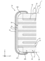
- FIG. 2 is a cross-sectional view of the multilayer ceramic capacitor taken along line AA in FIG.
- FIG. 3 is a cross-sectional view of the multilayer ceramic capacitor taken along line BB in FIG.
- FIG. 4 is a plan view showing an example of a protective metal layer on a laminate.
- FIG. 5 is a cross-sectional view showing an example of the layer structure of the external electrodes.
- FIG. 6 is an enlarged cross-sectional view of the boundary between the edge of the underlayer and the protective metal layer.
- FIG. 7 is a plan view showing an example of a circuit board on which a multilayer ceramic capacitor is mounted.
- FIG. 8 is a cross-sectional view showing an example of a protective metal layer covering a corner portion.
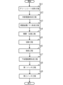
- FIG. 9 is a flowchart showing an example of a manufacturing process for a multilayer ceramic capacitor.
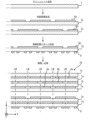
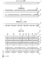
- FIG. 10 is a plan view showing an example of a green sheet forming step, an internal electrode forming step, a protective metal pattern forming step, and a lamination and compression bonding step.
- FIG. 11 is a flowchart showing another example of the manufacturing process for the multilayer ceramic capacitor.
- FIG. 12 is a plan view showing an example of a green sheet forming step, an internal electrode forming step, and a lamination and compression bonding step.
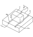
- FIG. 13 is a perspective view showing an example of a method for forming a protective metal pattern.
- FIG. 14 is a cross-sectional view taken along line CC of FIG.
- FIG. 15 is a plan view showing a modification of the protective metal pattern forming step and the lamination and compression bonding step shown in FIG.
- FIG. 1 is a perspective view showing an example of a multilayer ceramic capacitor 1.
- Fig. 2 is a cross-sectional view of the multilayer ceramic capacitor 1 taken along line AA in Fig. 1.
- Fig. 3 is a cross-sectional view of the multilayer ceramic capacitor 1 taken along line BB in Fig. 2.
- the multilayer ceramic capacitor 1 is an example of a multilayer ceramic electronic component.
- Other examples of multilayer ceramic electronic components include multilayer ceramic varistors and multilayer ceramic thermistors, but in this embodiment, a multilayer ceramic capacitor is used as a representative example.
- the multilayer ceramic capacitor 1 has a laminate 2 having a substantially rectangular parallelepiped shape, and external electrodes 3a, 3b provided on a pair of end faces 2A, 2B that face each other in a direction substantially perpendicular to the lamination direction of the laminate 2.
- FIGS. 1 to 3 show the mutually orthogonal X, Y, and Z directions.
- the X direction is the length (L) direction of the multilayer ceramic capacitor 1, and coincides with the direction in which a pair of end faces 2A, 2B of the laminate 2 face each other.
- the Y direction is the width (W) direction of the multilayer ceramic capacitor 1, and coincides with the direction in which a pair of side faces 2E, 2F of the laminate 2 face each other.
- the Z direction is the height (H) direction of the multilayer ceramic capacitor 1, and coincides with the lamination direction of the multilayer ceramic capacitor 1.
- the X direction is an example of a direction that is approximately orthogonal to the lamination direction.
- the X, Y, and Z directions are also shown as appropriate in FIG. 4 and subsequent figures.
- the laminate 2 has an upper surface 2C, a lower surface 2D, a pair of end surfaces 2A, 2B, a pair of side surfaces 2E, 2F, and corners 200, 210.
- the upper surface 2C and the lower surface 2D are generally flat surfaces that face each other
- the pair of end surfaces 2A, 2B are generally flat surfaces that face each other in the X direction
- the pair of side surfaces 2E, 2F are generally flat surfaces that face each other in the Y direction.
- the upper surface 2C, the lower surface 2D, and the side surfaces 2E, 2F are examples of four surfaces that are generally perpendicular to the end surfaces 2A, 2B.
- the corners 200, 210 are the ridges at the boundaries of the top surface 2C, the bottom surface 2D, the pair of end surfaces 2A, 2B, and the pair of side surfaces 2E, 2F, and the apex where multiple ridges come together.
- the corners 200 are curved portions that connect the adjacent end surfaces 2A, 2B and the top surface 2C, and the corners 210 are curved portions that connect the adjacent end surfaces 2A, 2B and the bottom surface 2D.
- the corners 200 are provided at both ends of the cover layer 20, and the corners 210 are provided at both ends of the cover layer 21.
- the dotted lines indicate the boundaries between the curved corners 200 and the substantially planar top surface 2C, and the boundaries between the curved corners 210 and the substantially planar bottom surface 2D.
- the laminate 2 has a laminated structure in which dielectric layers 22 containing a ceramic material that functions as a dielectric and internal electrode layers 23 are alternately laminated, and further laminated with a pair of cover layers 20, 21 sandwiching the dielectric layers 22 and internal electrode layers 23 from both sides in the lamination direction.
- the part in which the dielectric layers 22 and internal electrode layers 23 are alternately laminated is sometimes called the "capacitive layer.”
- the cover layers 20, 21 sandwich the capacitive layer from both sides in the lamination direction.
- side margin portions 220, 221 are provided on both sides in the width direction of the internal electrode layers 23 and the dielectric layers 22. The side margin portions 220, 221 sandwich the capacitive layer from both sides in the width direction.
- the internal electrode layers 23 face each other with the dielectric layer 22 therebetween in the stacking direction, and one end is alternately drawn out to the end faces 2A and 2B along the stacking direction.
- the internal electrode layers 23 are mainly composed of base metals such as Ni (nickel), Cu (copper), and Sn (tin).
- Noble metals such as Pt (platinum), Pd (palladium), Ag (silver), and Au (gold) or alloys containing these may also be used as the internal electrode layers 23.
- the thickness of the internal electrode layers 23 is, for example, 0.3 to 1.3 ( ⁇ m).
- the thickness of the internal electrode layers 23 is not limited to this, and may be, for example, 0.3 ( ⁇ m) or less, or 0.05 to 0.3 ( ⁇ m). Furthermore, the thickness of the internal electrode layers 23 may be 1.3 ( ⁇ m) or more, or 1.3 to 3.5 ( ⁇ m).
- the dielectric layer 22 has a main phase of a ceramic material having a perovskite structure represented by the general formula ABO 3.
- the perovskite structure includes ABO 3- ⁇ ( ⁇ is a small number) that is out of the stoichiometric composition.
- the ceramic material can be selected from at least one of BaTiO 3 (barium titanate), CaZrO 3 (calcium zirconate), CaTiO 3 (calcium titanate), SrTiO 3 (strontium titanate), MgTiO 3 (magnesium titanate), Ba 1-x-y Ca x Sr y Ti 1-z Zr z O 3 (0 ⁇ x ⁇ 1, 0 ⁇ y ⁇ 1, 0 ⁇ z ⁇ 1) that forms a perovskite structure, and the like.
- Ba 1-x-y Ca x Sr y Ti 1-z Zr z O 3 is barium strontium titanate, barium calcium titanate, barium zirconate, barium titanate zirconate, calcium titanate zirconate, barium calcium titanate zirconate, etc.
- the thickness of the dielectric layer 22 is, for example, 0.3 to 4.0 ( ⁇ m).
- the thickness of the dielectric layer 22 is not limited to this, and may be 0.3 ( ⁇ m) or less, or may be 0.05 to 0.3 ( ⁇ m).
- the thickness of the dielectric layer 22 may be 4.0 ( ⁇ m) or more, or may be 4.0 to 20.0 ( ⁇ m).
- the cover layers 20, 21 and the side margin portions 220, 221 are also formed primarily from ceramic material, just like the dielectric layer 22.
- protective metal layers 4a and 4b are provided between the ends of the external electrodes 3a and 3b on the bottom surface 2D and the side surfaces 2E and 2F, respectively, and the surface of the laminate 2.
- the protective metal layers 4a and 4b are mainly composed of Ni, for example.
- the protective metal layers 4a and 4b are an example of a second metal layer, and Ni is an example of a second metal.
- the external electrodes 3a, 3b cover the end faces 2A, 2B of the laminate 2 that face each other in the longitudinal direction of the multilayer ceramic capacitor 1.
- the external electrodes 3a, 3b also extend onto the upper surface 2C, the lower surface 2D, and the side surfaces 2E, 2F. However, the external electrodes 3a, 3b are spaced apart from each other on the surfaces of the upper surface 2C, the lower surface 2D, and the side surfaces 2E, 2F.
- FIG. 4 is a plan view showing an example of protective metal layers 4a, 4b on a laminate 2.
- components common to FIGS. 1 to 3 are given the same reference numerals, and their explanation is omitted.
- external electrodes 3a, 3b are indicated by dotted lines.
- the protective metal layers 4a and 4b are strip-shaped metal films provided on the lower surface 2D along the width direction of the laminate 2.
- the protective metal layers 4a and 4b extend from both ends on the lower surface 2D to the side surfaces 2E and 2F.
- a portion of the protective metal layer 4a in the width direction is sandwiched between the external electrode 3a and the laminate 2, and the remaining portion is exposed from the external electrode 3a.
- a portion of the protective metal layer 4b in the width direction is sandwiched between the external electrode 3b and the laminate 2, and the remaining portion is exposed from the external electrode 3b.
- the protective metal layers 4a, 4b are formed so as to have a width on the inner ends of the external electrodes 3a, 3b from the bottom surface 2D to the side surfaces 2E, 2F.
- the protective metal layers 4a, 4b protect the laminate 2 from stress and moisture.
- the protective metal layers 4a, 4b are provided from the entire width direction of the bottom surface 2D to the side surfaces 2E, 2F, but may be provided only on a part of the bottom surface 2D.
- the protective metal layers 4a, 4b are provided only in the region on the bottom surface 2D side in the stacking direction of the side surfaces 2E, 2F, but may be provided over the entire stacking direction of the side surfaces 2E, 2F.
- the protective metal layers 4a, 4b may also be provided on the top surface 2C.
- Fig. 5 is a cross-sectional view showing an example of the layer structure of the external electrode 3a.
- Fig. 5 shows a cross-sectional view of the laminate 2 taken along a direction substantially perpendicular to the end face 2A and the upper face 2C and lower face 2D adjacent thereto.
- the same components as those in Fig. 2 are given the same reference numerals and their description will be omitted.
- Fig. 5 shows only one external electrode 3a, but the other external electrode 3b also has the same structure as the external electrode 3a.
- the external electrode 3a includes a base electrode layer 30, an internal plating layer 31, and an external plating layer 32.
- the base electrode layer 30, the internal plating layer 31, and the external plating layer 32 are stacked in this order from the laminate 2 side.
- the base electrode layer 30 is an example of a first metal layer.
- the base electrode layer 30 covers the end face 2A so as to be electrically connected to the internal electrode layer 23, and extends from the end face 2A to each end of the lower face 2D and the upper face 2C via the corners 210 and 200, respectively.
- the base electrode layer 30 is mainly composed of, for example, Cu, and contains a glass component for densifying the base electrode layer 30 and a co-material for controlling the sintering property of the base electrode layer 30.
- Cu is an example of a first metal.
- the base electrode layer 30 has good adhesion to the dielectric layer 22 and the cover layers 20 and 21, which are mainly composed of a ceramic material.
- the main component of the base electrode layer 30 may be other metals such as Ni, Al (aluminum), and Zn (zinc).
- the internal plating layer 31 covers the base electrode layer 30.
- the internal plating layer 31 is formed by a plating process using a metal such as Ni.
- the outer plating layer 32 covers the inner plating layer 31.
- the outer plating layer 32 is formed by a plating process using a metal such as Sn.
- the protective metal layer 4a has a predetermined width in the longitudinal direction of the laminate 2, and extends from between the end 300 of the base electrode layer 30 on the bottom surface 2D and the bottom surface 2D toward the other external electrode 3b. A portion of the protective metal layer 4a is sandwiched not only between the end 300 of the base electrode layer 30 on the bottom surface 2D, but also between the bottom surface 2D and each end of the internal plating layer 31 and the external plating layer 32 on the bottom surface 2D. The other portion of the protective metal layer 4a on the other external electrode 3b side is exposed on the bottom surface 2D.
- the thickness of the protective metal layer 4a is 1.0 to 1.5 ( ⁇ m) or more, since sufficient strength can be obtained even when taking into account the oxide film formed by firing.
- the protective metal layer 4a is excessively thick, the external electrode 3a is essentially extended in the longitudinal direction, and the effect of dispersing stress on the laminate 2, which will be described later, is reduced compared to when the protective metal layer 4a is thin. For this reason, it is preferable that the thickness of the protective metal layer 4a is 2.0 ( ⁇ m) or less.
- the protective metal layer 4a is disposed between the base electrode layer 30 and the laminate 2 to protect the capacitive portion of the laminate 2 from moisture intrusion.
- a specific example of the configuration is described below.
- FIG. 6 is an enlarged cross-sectional view of the boundary between the end 300 of the base electrode layer 30 and the protective metal layer 4a.
- the same components as in FIG. 5 are denoted by the same reference numerals, and their description will be omitted.
- the protective metal layer 4a has an alloy region 40 formed along a contact surface 41 in contact with the base electrode layer 30.
- the alloy region 40 is a region formed by Cu at the end 300 of the base electrode layer 30 diffusing into the protective metal layer 4a when the base electrode layer 30 is baked in the manufacturing process of the multilayer ceramic capacitor 1, and contains an alloy of Cu and Ni. Therefore, the protective metal layer 4a is firmly joined to the end 300 of the base electrode layer 30 by the alloy region 40, and there is substantially no gap between the protective metal layer 4a and the end 300 of the base electrode layer 30. This prevents moisture from entering from the end 300 of the base electrode layer 30.
- the protective metal layer 4a extends from between the end 300 of the base electrode layer 30 and the bottom surface 2D along the bottom surface 2D toward the other external electrode 3b. Therefore, if moisture penetrates between the bottom surface 2D and the protective metal layer 4a, the penetration path is longer than when the protective metal layer 4a is not provided, so it is difficult for moisture to penetrate. This improves the water resistance of the multilayer ceramic capacitor 1.
- the protective metal layer 4a also protects the laminate 2 from stress applied from the vicinity of the tip of the external electrodes 3a, 3b due to thermal expansion or impact during firing of the external electrodes 3a, 3b. If the protective metal layer 4a were not present, the stress applied to the laminate 2 would be concentrated at the tip position Pa of the end 300 of the base electrode layer 30. On the other hand, if the protective metal layer 4a is present, the protective metal layer 4a can distribute the stress generated during firing of the base electrode layer 30 to the region R from the tip position Pa to the end position Pb of the protective metal layer 4a on the other external electrode 3b side, thereby mitigating the stress applied near the tip of the external electrode 3a. An example of the stress when a circuit board on which the multilayer ceramic capacitor 1 is mounted is warped will be described later.
- an oxide film 42 is formed on the outer surface of the protective metal layer 4a.
- the oxide film 42 is formed, for example, by firing a Ni conductive paste during the manufacturing process of the multilayer ceramic capacitor 1.
- the oxide film 42 is weaker than the other parts (inside) of the protective metal layer 4a. Therefore, when stress is applied from the external electrode 3a, the oxide film 42 breaks, making it possible to relieve the stress.
- a similar oxide film is also formed on the other protective metal layer 4b, making it possible to relieve the stress of the external electrode 3b.
- FIG. 7 is a plan view showing an example of a circuit board 5 on which a multilayer ceramic capacitor 1 is mounted.
- FIG. 7 shows the normal state of the circuit board 5 before it is bent, and the state of the circuit board 5 when it is bent.
- components common to FIG. 1 are given the same reference numerals, and their description will be omitted.
- the multilayer ceramic capacitor 1 and the circuit board 5 are part of an electronic device 50, such as a smartphone or a computer.
- the multilayer ceramic capacitor 1 is mounted with the external electrodes 3a and 3b in contact with the electrode pads 5a and 5b on the circuit board 5, respectively.
- the bottom surface 2D is the mounting surface that faces the plate surface of the circuit board 5.
- the external electrodes 3a, 3b are electrically connected to the electrode pads 5a, 5b, respectively, by solder H. Note that the outline of the portion of the solder H that overlaps with the multilayer ceramic capacitor 1 in a front view is shown by a dotted line.
- a pulling force f acts on the tips of the external electrodes 3a, 3b towards the circuit board 5 and outside the multilayer ceramic capacitor 1.
- a stress F acts on the underside 2D of the laminate 2 in the opposite direction to the pulling force f.
- the stress F is mitigated by the protective metal layers 4a, 4b, preventing cracks from occurring in the laminate 2.
- the multilayer ceramic capacitor 1 of this embodiment can suppress the occurrence of cracks and improve moisture resistance. This improves the reliability of the multilayer ceramic capacitor 1.
- the main component of the base electrode layer 30 is Cu
- the main component of the protective metal layers 4a and 4b is Ni, which has the advantage that a strong interface can be formed by alloying Cu and Ni during firing, but the main components of each are not limited to this.
- the main components of the protective metal layers 4a and 4b may also be metals such as W (tungsten), Cr (chromium), Fe (iron), and Ti (titanium) that can form an alloy with Cu.
- the protective metal layers 4a, 4b extend from the bottom surface 2D to the side surfaces 2E, 2F. Therefore, the protective metal layers 4a, 4b can suppress moisture intrusion and cracks on the side surfaces 2E, 2F as well as on the bottom surface 2D.
- the protective metal layers 4a, 4b may be provided on only the bottom surface 2D or only one of the side surfaces 2E, 2F, or only on the bottom surface 2D.
- the protective metal layers 4a, 4b may cover not only the bottom surface 2D but also the adjacent corners 210 as follows.
- FIG. 8 is a cross-sectional view showing an example of a protective metal layer 4c that covers a corner portion 210.
- the same components as in FIG. 5 are given the same reference numerals, and their description will be omitted.
- the protective metal layer 4c extends from between the end 300 of the base electrode layer 30 and the bottom surface 2D to the corner 210 between the bottom surface 2D and the end surface 2A. Therefore, compared to the case where the protective metal layer 4a does not cover the corner 210 as shown in FIG. 5, the contact area between the protective metal layer 4c and the base electrode layer 30 is larger, and the alloy region 40 is also larger. Therefore, the bond between the protective metal layer 4c and the base electrode layer 30 is stronger.
- the protective metal layers 4a, 4b are provided from the lower surface 2D to the ends of the side surfaces 2E, 2F on the lower surface 2D side, but are not limited to this.
- the protective metal layers 4a, 4b may be provided from the upper surface 2C to the ends of the side surfaces 2E, 2F on the upper surface 2C side.
- the protective metal layers 4a, 4b may also be provided from at least one of the side surfaces 2E, 2F to the ends of the upper surface 2C and the lower surface 2D on the side surface 2E, 2F side. In this way, the protective metal layers 4a, 4b are provided on at least one of the upper surface 2C, the lower surface 2D, and the side surfaces 2E, 2F, and extend from that one surface to the ends of a pair of adjacent surfaces.
- the multilayer ceramic capacitor 1 is mounted on the circuit board 5 with the side surfaces 2E, 2F on which the protective metal layers 4a, 4b are provided as the mounting surface, unlike FIG. 7.
- the circuit board 5 warps, the intrusion of moisture at the side surfaces 2E, 2F, upper surface 2C, and lower surface 2D, and the occurrence of cracks in the laminate 2 are suppressed, just as when the lower surface 2D is used as the mounting surface.
- (Manufacturing process of multilayer ceramic capacitors) 9 is a flow chart showing an example of a manufacturing process for the multilayer ceramic capacitor 1. This manufacturing process is an example of a method for manufacturing a multilayer ceramic electronic component.
- FIG. 10 is a plan view showing an example of the green sheet forming process St1, the internal electrode forming process St2, the protective metal pattern forming process St3, and the lamination and pressure bonding process St4.
- the manufacturing process will be described below with reference to FIG. 9 and FIG. 10.
- the manufacturing process of a multilayer ceramic capacitor 1 in which protective metal layers 4a, 4b are not provided on the side surfaces 2E, 2F, but only on the bottom surface 2D is described.
- a green sheet forming step St1 is performed.
- a binder such as polyvinyl butyral (PVB) resin, an organic solvent such as ethanol or toluene, and a plasticizer are added to a dielectric material obtained by adding various additive compounds (such as sintering aids) to ceramic powder, and then wet-mixed.
- the obtained slurry is used to coat a dielectric green sheet 7 on a substrate by, for example, a die coater method or a doctor blade method, and then dried.
- the substrate is, for example, a PET (polyethylene terephthalate) film.
- Additive compounds used in ceramic powder include oxides of Mg (magnesium), Mn (manganese), V (vanadium), Cr (chromium), rare earth elements (Y (yttrium), Sm (samarium), Eu (europium), Gd (gadolinium), Tb (terbium), Dy (dysprosium), Ho (holmium), Er (erbium), Tm (thulium) and Yb (ytterbium)), as well as oxides or glasses of Co (cobalt), Ni, Li (lithium), B (boron), Na (sodium), K (potassium) and Si (silicon).
- an internal electrode forming step St2 is performed.
- a conductive paste containing ceramic particles is applied to the surfaces of the dielectric green sheets 7a and 7b of the dielectric green sheet 7 to form the internal electrodes.
- the electrode patterns 6a and 6b are formed.
- the internal electrode patterns 6a and 6b have shapes corresponding to the internal electrode layers 23. Specifically, the internal electrode patterns 6a and 6b are arranged in the X-axis direction so as to be shifted from each other by a pitch. It is formed by shifting the position.
- a metal conductive paste for forming internal electrodes containing an organic binder is printed on the dielectric green sheets 7a, 7b on the substrate by gravure printing or the like to form a film of multiple internal electrode patterns 6a, 6b spaced apart from one another.
- Ceramic particles are added to the conductive paste as a co-material.
- the main component of the ceramic particles is not particularly limited, but is preferably the same as the main ceramic component of the dielectric layer 22.
- the internal electrode patterns 6a, 6b are not limited to being printed, and may be formed by sputtering, for example.
- the protective metal pattern forming step St3 is carried out.
- a protective metal pattern 8 is formed on the side opposite the internal electrode pattern 6b of one of the dielectric green sheets 7d, of the dielectric green sheets 7b on which the internal electrode pattern 6b is formed.
- the protective metal pattern 8 becomes the protective metal layers 4a, 4b after the laminate 2 is fired.
- the protective metal pattern 8 is printed on the back surface of the internal electrode pattern 6b, for example, by the same method as for the internal electrode patterns 6a, 6b.
- the protective metal pattern 8 is printed on both sides of the cut line LW in the cutting step St5 so that it is positioned near the external electrodes 3a, 3b.
- the protective metal pattern 8 may be formed on one of the dielectric green sheets 7a on which the other internal electrode pattern 6a is formed.
- the protective metal pattern 8 may also be formed by sputtering instead of printing.
- the lamination and compression step St4 is performed.
- multiple dielectric green sheets 7a to 7d are laminated and compressed with the protective metal pattern 8 as the outermost layer and the internal electrode patterns 6a, 6b facing each other via the dielectric green sheets 7a, 7b.
- multiple dielectric green sheets 7a to 7d are laminated and compressed with the dielectric green sheet 7d, on which the protective metal pattern 8 is printed, as the bottom layer so that the surface of the protective metal pattern 8 is exposed in the stacking direction.
- the compression means can be, for example, a hydrostatic press, but is not limited to this.
- a cutting step St5 is performed.
- the laminated sheet 7S obtained by compression bonding is divided into a plurality of laminates each having a substantially rectangular parallelepiped shape.
- the laminated sheet is cut in the lamination direction along a predetermined cutting line LW with a blade to expose the ends of the internal electrode patterns 6a and 6b. This results in a plurality of pre-fired laminates 2.
- a firing step St6 is performed.
- the laminate 2 before firing is subjected to a binder removal process in an N2 atmosphere at 250 to 500°C, and then fired at a firing temperature of 1200°C or higher for about one hour in a reducing atmosphere with an oxygen partial pressure of 0.003 (Pa), thereby sintering each particle in the laminate 2.
- the dielectric green sheets 7a to 7c become the cover layers 20, 21, the side margins 220, 221, and the dielectric layer 22, and the internal electrode patterns 6a, 6b become the internal electrode layers 23.
- the protective metal pattern 8 is baked on the laminate 2, thereby forming the protective metal layers 4a, 4b extending from the lower surface 2D to the side surfaces 2E, 2F.
- an oxide film 42 is formed on the outer surfaces of the protective metal layers 4a, 4b by firing.
- a base electrode layer forming step St7 is performed.
- This step is a step of applying a conductive paste having a different main component from that of the protective metal pattern 8 to the laminate 2, and baking the conductive paste to form the internal electrode patterns 6a,
- a conductive paste containing glass frit, a binder, and a solvent is applied to the laminate 2 by, for example, a dipping method.
- the main component of the conductive paste is different from that of the protective metal layers 4a and 4b.
- the conductive paste is applied to the end faces 2A, 2B, both longitudinal ends of the side faces 2E, 2F, both longitudinal ends of the top face 2C, and both longitudinal ends of the bottom face 2D of the laminate 2. At this time, the conductive paste is applied so as to contact the internal electrode layer 23 drawn out to the end faces 2A, 2B, and to cover the area from the end faces 2A, 2B to the portions of the surfaces of the protective metal layers 4a, 4b on the bottom face 2D that are on the side of the end faces 2A, 2B.
- the conductive paste is dried and baked to form the base electrode layer 30.
- the heat from the baking process causes the main metal of the base electrode layer 30 (e.g., Cu) to diffuse toward the protective metal layers 4a and 4b.
- the diffused metal combines with the main metal of the protective metal layers 4a and 4b (e.g., Ni) to form an alloy.
- alloy regions 40 are formed in the protective metal layers 4a and 4b along the contact surfaces 41 that are in contact with the base electrode layer 30.
- a first plating step St8 is performed.
- an inner plating layer 31 is formed so as to cover the base electrode layer 30 by, for example, electrolytic plating.
- a second plating step St9 is performed.
- an outer plating layer 32 that covers the inner plating layer 31 is formed by, for example, electrolytic plating.
- the multilayer ceramic capacitor 1 is manufactured.
- the protective metal layers 4a, 4b can be formed by the same method as the internal electrode layers 23, so that the multilayer ceramic capacitor 1 can be manufactured easily.
- FIG. 11 is a flow chart showing another example of the manufacturing process of the multilayer ceramic capacitor 1.
- the same steps as in Fig. 9 are denoted by the same reference numerals, and the description thereof will be omitted.
- a protective metal pattern is formed after the formation of the pre-fired laminate 2.
- FIG. 12 is a plan view showing an example of the green sheet forming process St1, the internal electrode forming process St2, and the lamination and compression bonding process St4a. The manufacturing process will be described below with reference to FIG. 11 and FIG. 12.
- a laminated sheet 7S is formed by laminating and pressure bonding a plurality of dielectric green sheets 7a, 7b on which the internal electrode patterns 6a, 6b that become the internal electrode layers 23 are printed, and a dielectric green sheet 7c on which the internal electrode patterns 6a, 6b are not printed.
- the dielectric green sheets 7a, 7b are alternately laminated in the lamination direction so that the internal electrode patterns 6a, 6b are alternately drawn out, and the dielectric green sheet 7c is laminated on the upper part of the plurality of dielectric green sheets 7a, 7b.
- the dielectric green sheets 7a and 7b are stacked so that the internal electrode patterns 6a and 6b face each other via the dielectric green sheets 7a and 7b.
- the stacked dielectric green sheets 7a to 7c are pressed together to bond them together.
- the cutting step St5 is carried out in the same manner as above, and the pre-fired laminate 2 is obtained.
- a protective metal pattern forming step St5a is performed.
- a protective metal pattern that becomes the protective metal layers 4a and 4b is formed on the lower surface 2D, which is one of the six surfaces of the laminate 2 and is substantially perpendicular to the lamination direction.
- FIG. 13 is a perspective view showing an example of a method for forming a protective metal pattern. Also, FIG. 14 is a cross-sectional view taken along line C-C in FIG. 13.
- the protective metal layers 4a, 4b are formed by pressing the bottom surface 2D of the fired laminate 2 against a pair of grooves 90, 91 formed in a base 9 made of an elastic material such as rubber, as indicated by arrow G.
- the pair of grooves 90, 91 are filled with conductive paste 90a, 91a for forming a protective metal pattern 900.
- the base 9 is depressed by pressure, so that the conductive paste 90a in the groove 90 is applied not only to the bottom surface 2D, but also to the areas of the side surfaces 2E and 2F close to the bottom surface 2D.
- the conductive paste 91a in the other groove 91 is also applied to the bottom surface 2D and the side surfaces 2E and 2F in the same manner. In this way, a protective metal pattern 900 made of the conductive pastes 90a and 91a is formed on the laminate 2.
- the protective metal pattern 900 is formed from the bottom surface 2D to the ends of the side surfaces 2E and 2F by pressing the bottom surface 2D against the grooves 90 and 91 of the base 9, but it is also possible to form the protective metal pattern 900 from one side surface 2E, 2F to the ends of the top surface 2C and bottom surface 2D by pressing, for example, one of the side surfaces 2E, 2F against the grooves 90 and 91 of the base 9.
- the protective metal pattern 900 is formed on at least one of the four surfaces that are approximately perpendicular to the end surfaces 2A and 2B of the laminate 2.
- the protective metal pattern 900 may also be formed by printing or sputtering.
- the firing process St6 is performed.
- the protective metal pattern 900 is baked to form protective metal layers 4a, 4b on the laminate 2, which extend from the bottom surface 2D to the side surfaces 2E, 2F.
- oxide films 42 are formed on the outer surfaces of the protective metal layers 4a, 4b by firing.
- the external electrodes 3a, 3b of the multilayer ceramic capacitor 1 of this embodiment do not include a resin electrode layer, but a resin electrode layer may be formed by applying a resin paste to the base electrode layer 30 during the manufacturing process.
- Fig. 15 is a plan view showing a modified example of the protective metal pattern forming step St3 and the lamination and pressure bonding step St4 shown in Fig. 10.
- the same reference numerals are used for the configurations common to Fig. 10, and the description thereof will be omitted.
- a protective metal pattern 8 is formed on one side of the dielectric green sheet 7e on which the internal electrode patterns 6a, 6b are not formed.
- the protective metal pattern 8 becomes the protective metal layers 4a, 4b after the laminate 2 is fired.
- multiple dielectric green sheets 7a to 7c, 7d are laminated and compressed with the protective metal pattern 8 as the outermost layer and the internal electrode patterns 6a, 6b facing each other via the dielectric green sheets 7a, 7b.
- multiple dielectric green sheets 7a to 7c, 7d are laminated and compressed with the dielectric green sheet 7e, on which the protective metal pattern 8 is printed, as the bottom layer so that the surface of the protective metal pattern 8 is exposed in the lamination direction.
- the dielectric green sheet 7c, on which the internal electrode patterns 6a, 6b are not printed is laminated as the outermost layer on the opposite side to the dielectric green sheet 7e, on which the protective metal pattern 8 is printed.
- the cutting step St5 is performed in the same manner as above, and the pre-fired laminate 2 is obtained.
Landscapes
- Engineering & Computer Science (AREA)
- Microelectronics & Electronic Packaging (AREA)
- Power Engineering (AREA)
- Physics & Mathematics (AREA)
- Electromagnetism (AREA)
- Ceramic Engineering (AREA)
- Manufacturing & Machinery (AREA)
- Fixed Capacitors And Capacitor Manufacturing Machines (AREA)
- Ceramic Capacitors (AREA)
Priority Applications (1)
| Application Number | Priority Date | Filing Date | Title |
|---|---|---|---|
| JP2025506538A JPWO2024190120A1 (https=) | 2023-03-10 | 2024-01-30 |
Applications Claiming Priority (2)
| Application Number | Priority Date | Filing Date | Title |
|---|---|---|---|
| JP2023037971 | 2023-03-10 | ||
| JP2023-037971 | 2023-03-10 |
Publications (1)
| Publication Number | Publication Date |
|---|---|
| WO2024190120A1 true WO2024190120A1 (ja) | 2024-09-19 |
Family
ID=92754819
Family Applications (1)
| Application Number | Title | Priority Date | Filing Date |
|---|---|---|---|
| PCT/JP2024/002793 Ceased WO2024190120A1 (ja) | 2023-03-10 | 2024-01-30 | 積層セラミック電子部品、電子装置、及び積層セラミック電子部品の製造方法 |
Country Status (2)
| Country | Link |
|---|---|
| JP (1) | JPWO2024190120A1 (https=) |
| WO (1) | WO2024190120A1 (https=) |
Citations (5)
| Publication number | Priority date | Publication date | Assignee | Title |
|---|---|---|---|---|
| JPS6386414A (ja) * | 1986-09-30 | 1988-04-16 | 太陽誘電株式会社 | 積層形セラミツクコンデンサ |
| JPH0465106A (ja) * | 1990-07-05 | 1992-03-02 | Murata Mfg Co Ltd | 複合部品 |
| JP2019004080A (ja) * | 2017-06-16 | 2019-01-10 | 太陽誘電株式会社 | 電子部品、電子装置、及び電子部品の製造方法 |
| JP2019096824A (ja) * | 2017-11-27 | 2019-06-20 | 太陽誘電株式会社 | 積層セラミックコンデンサ及び積層セラミックコンデンサの製造方法 |
| JP2023025982A (ja) * | 2021-08-12 | 2023-02-24 | 太陽誘電株式会社 | セラミック電子部品及び回路基板 |
-
2024
- 2024-01-30 JP JP2025506538A patent/JPWO2024190120A1/ja active Pending
- 2024-01-30 WO PCT/JP2024/002793 patent/WO2024190120A1/ja not_active Ceased
Patent Citations (5)
| Publication number | Priority date | Publication date | Assignee | Title |
|---|---|---|---|---|
| JPS6386414A (ja) * | 1986-09-30 | 1988-04-16 | 太陽誘電株式会社 | 積層形セラミツクコンデンサ |
| JPH0465106A (ja) * | 1990-07-05 | 1992-03-02 | Murata Mfg Co Ltd | 複合部品 |
| JP2019004080A (ja) * | 2017-06-16 | 2019-01-10 | 太陽誘電株式会社 | 電子部品、電子装置、及び電子部品の製造方法 |
| JP2019096824A (ja) * | 2017-11-27 | 2019-06-20 | 太陽誘電株式会社 | 積層セラミックコンデンサ及び積層セラミックコンデンサの製造方法 |
| JP2023025982A (ja) * | 2021-08-12 | 2023-02-24 | 太陽誘電株式会社 | セラミック電子部品及び回路基板 |
Also Published As
| Publication number | Publication date |
|---|---|
| JPWO2024190120A1 (https=) | 2024-09-19 |
Similar Documents
| Publication | Publication Date | Title |
|---|---|---|
| CN109920644B (zh) | 陶瓷电子器件及陶瓷电子器件的制造方法 | |
| CN109559892B (zh) | 陶瓷电子器件和陶瓷电子器件的制造方法 | |
| US11705281B2 (en) | Multilayer ceramic capacitor and method of manufacturing the same | |
| JP2025170129A (ja) | 積層セラミックコンデンサ | |
| US11170937B2 (en) | Multilayer ceramic electronic component | |
| JP7651263B2 (ja) | 積層セラミックコンデンサおよびその製造方法 | |
| JP2021082685A (ja) | セラミック電子部品およびその製造方法 | |
| KR20230109095A (ko) | 적층 세라믹 전자 부품 및 그 제조 방법 | |
| JP2003022929A (ja) | 積層セラミックコンデンサ | |
| JP2012009556A (ja) | セラミック電子部品及びその製造方法 | |
| JP7312525B2 (ja) | 積層セラミックコンデンサおよびその製造方法 | |
| JP7122085B2 (ja) | 積層セラミックコンデンサおよびその製造方法 | |
| JP7744182B2 (ja) | セラミック電子部品およびその製造方法 | |
| WO2024190120A1 (ja) | 積層セラミック電子部品、電子装置、及び積層セラミック電子部品の製造方法 | |
| US20250201477A1 (en) | Multilayer ceramic electronic device and manufacturing method of the same | |
| WO2024180930A1 (ja) | 積層セラミック電子部品及びその製造方法 | |
| US20250372306A1 (en) | Multilayer ceramic electronic component and method of manufacturing the same | |
| JP7653799B2 (ja) | セラミック電子部品、回路基板およびセラミック電子部品の製造方法 | |
| US20240331945A1 (en) | Multilayer ceramic electronic device | |
| US20240404755A1 (en) | Multilayer ceramic capacitor | |
| US20260018345A1 (en) | Multilayer ceramic electronic component and method of manufacturing the same | |
| US20240412924A1 (en) | Multilayer ceramic electronic device, manufacturing method of the same, and circuit board | |
| JP2024009507A (ja) | セラミック電子部品及びその製造方法 | |
| WO2024127806A1 (ja) | 積層セラミック電子部品及びその製造方法 | |
| WO2024166553A1 (ja) | 積層セラミック電子部品及びその製造方法 |
Legal Events
| Date | Code | Title | Description |
|---|---|---|---|
| 121 | Ep: the epo has been informed by wipo that ep was designated in this application |
Ref document number: 24770240 Country of ref document: EP Kind code of ref document: A1 |
|
| WWE | Wipo information: entry into national phase |
Ref document number: 2025506538 Country of ref document: JP |
|
| NENP | Non-entry into the national phase |
Ref country code: DE |
|
| 122 | Ep: pct application non-entry in european phase |
Ref document number: 24770240 Country of ref document: EP Kind code of ref document: A1 |