WO2024190083A1 - 電圧検出回路および時計 - Google Patents
電圧検出回路および時計 Download PDFInfo
- Publication number
- WO2024190083A1 WO2024190083A1 PCT/JP2024/001690 JP2024001690W WO2024190083A1 WO 2024190083 A1 WO2024190083 A1 WO 2024190083A1 JP 2024001690 W JP2024001690 W JP 2024001690W WO 2024190083 A1 WO2024190083 A1 WO 2024190083A1
- Authority
- WO
- WIPO (PCT)
- Prior art keywords
- fine adjustment
- resistor
- coarse adjustment
- resistors
- resistance value
- Prior art date
- Legal status (The legal status is an assumption and is not a legal conclusion. Google has not performed a legal analysis and makes no representation as to the accuracy of the status listed.)
- Ceased
Links
Images




Classifications
-
- G—PHYSICS
- G01—MEASURING; TESTING
- G01R—MEASURING ELECTRIC VARIABLES; MEASURING MAGNETIC VARIABLES
- G01R19/00—Arrangements for measuring currents or voltages or for indicating presence or sign thereof
- G01R19/165—Indicating that current or voltage is either above or below a predetermined value or within or outside a predetermined range of values
-
- G—PHYSICS
- G04—HOROLOGY
- G04C—ELECTROMECHANICAL CLOCKS OR WATCHES
- G04C10/00—Arrangements of electric power supplies in time-pieces
-
- G—PHYSICS
- G04—HOROLOGY
- G04G—ELECTRONIC TIME-PIECES
- G04G19/00—Electric power supply circuits specially adapted for use in electronic time-pieces
- G04G19/02—Conversion or regulation of current or voltage
Definitions
- the present invention relates to a voltage detection circuit and a watch.
- Patent Document 1 discloses a voltage detection circuit that includes a resistive voltage divider circuit with a coarse adjustment variable resistor circuit and a fine adjustment variable resistor circuit, a coarse adjustment unit that controls the coarse adjustment variable resistor circuit, a fine adjustment unit that controls the fine adjustment variable resistor circuit, and a control unit that controls the coarse adjustment unit and the fine adjustment unit in response to a detection signal from a comparison circuit.
- a voltage detection circuit it is desirable to improve the detection resolution without increasing the circuit size. For example, it is preferable to improve the detection resolution while suppressing the number of resistors.
- the object of the present invention is to provide a voltage detection circuit and a watch that solves the above problems.
- the voltage detection circuit of the present invention comprises a comparator having a first input terminal to which a reference voltage is input and a second input terminal, a plurality of fine adjustment resistors arranged between the detection target and the second input terminal, at least one coarse adjustment resistor arranged between the detection target and the second input terminal, a fine adjustment switch section that connects an arbitrary number of the fine adjustment resistors in series to the detection target and the coarse adjustment resistors, a coarse adjustment switch section that connects an arbitrary number of the coarse adjustment resistors in series to the detection target and the fine adjustment resistors, and a control section that controls the opening and closing operation of the switches of the fine adjustment switch section and the opening and closing operation of the switches of the coarse adjustment switch section, and is characterized in that the coarse adjustment resistor includes a resistor having a resistance value equal to the total value obtained by adding up the resistance values of the plurality of fine adjustment resistors.
- the voltage detection circuit according to the present invention comprises a plurality of fine adjustment resistors, a coarse adjustment resistor arranged between the detection target and the second input terminal of the comparator, a fine adjustment switch section that connects any number of fine adjustment resistors in series to the detection target and the coarse adjustment resistors, and a coarse adjustment switch section that connects any number of coarse adjustment resistors in series to the detection target and the fine adjustment resistors.
- the coarse adjustment resistors include a resistor having a resistance value equal to the total value obtained by adding together the resistance values of the plurality of fine adjustment resistors.
- the voltage detection circuit according to the present invention has the effect of improving detection resolution by combining the fine adjustment resistors and the coarse adjustment resistors.
- FIG. 1 is a diagram showing a timepiece according to an embodiment of the present invention.
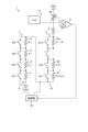
- FIG. 2 is a diagram illustrating a voltage detection circuit according to an embodiment.
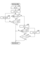
- FIG. 3 is a flowchart showing the operation of the voltage detection circuit according to the embodiment.
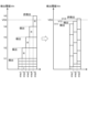
- FIG. 4 is a diagram of a detection sequence according to an embodiment.
- FIG. 5 is a diagram of a detection sequence according to an embodiment.
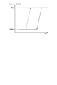
- FIG. 6 is a diagram showing the detection characteristics of the comparator.
- FIG. 7 is a diagram of a voltage detection circuit according to a first modified example of the embodiment.
- FIG. 8 is a diagram of a voltage detection circuit according to a second modification of the embodiment.
- a timepiece 1 As shown in Figure 1, a timepiece 1 according to this embodiment has an exterior case 2, a battery 4, a crystal 5, a voltage detection circuit 6, a dial 31, a second hand 32, a minute hand 33, and an hour hand 34.
- the timepiece 1 of this embodiment is an electronic timepiece, and calculates the internal time based on a clock signal generated by an oscillation circuit.
- the outer case 2 has a roughly cylindrical case body 21.
- the battery 4, voltage detection circuit 6, dial 31, second hand 32, minute hand 33, and hour hand 34 are housed in the case body 21.
- the crystal 5 is a transparent member that closes the opening on the front side of the outer case 2.
- the opening on the back side of the outer case 2 is closed by a back cover.
- Battery 4 is a rechargeable secondary battery.
- Clock 1 calculates the internal time using power supplied from battery 4, and moves second hand 32, minute hand 33, and hour hand 34.
- Clock 1 may also have a power generation unit such as a solar cell. In this case, the power generated by the power generation unit is stored in battery 4.
- the voltage detection circuit 6 is a circuit that detects the voltage of the battery 4 as the power source VSS. As shown in FIG. 2, the voltage detection circuit 6 has a comparator 3, a first resistor group 7 for fine adjustment, a second resistor group 8 for coarse adjustment, a fine adjustment switch section 9, a coarse adjustment switch section 10, a variable resistor VR, and a control section 50.
- the comparator 3 is a comparator and has a first input terminal 3a and a second input terminal 3b.
- a predetermined reference voltage Vref is input to the first input terminal 3a.
- the reference voltage Vref may be generated from the output voltage of the power supply VSS.
- An input voltage VM is input to the second input terminal 3b.
- the input voltage VM is a voltage obtained by dividing the voltage of the power supply VSS by the first resistor group 7, the second resistor group 8, and the variable resistor VR.
- the potential of the power supply VSS with respect to the ground potential VDD is, for example, a negative value.
- Comparator 3 outputs a signal according to the result of comparing the reference voltage Vref with the input voltage VM.
- comparator 3 outputs a detection signal when the potential of the input voltage VM is lower than the potential of the reference voltage Vref.
- the detection signal is, for example, a high-level ON signal.
- comparator 3 outputs a non-detection signal when the potential of the input voltage VM is higher than the potential of the reference voltage Vref.
- the non-detection signal is, for example, a low-level OFF signal.
- the first resistor group 7, the second resistor group 8, and the variable resistor VR are arranged in series in this order from the power supply VSS side to the ground potential VDD side.
- the variable resistor VR may be a switching type resistor device having multiple resistors, or may be a potentiometer.
- the variable resistor VR changes the resistance value between the second input terminal 3b and the ground potential VDD.
- the variable resistor VR is controlled by, for example, the control unit 50.
- the first resistor group 7 and the second resistor group 8 are arranged between the power supply VSS and the second input terminal 3b.
- the second resistor group 8 is a resistor that roughly adjusts the total resistance value between the power supply VSS and the second input terminal 3b.
- the first resistor group 7 is a resistor that finely adjusts the total resistance value between the power supply VSS and the second input terminal 3b.
- the plurality of fine adjustment resistors ri have the same resistance value r [ ⁇ ].
- the plurality of fine adjustment resistors ri are connected continuously and in series.
- the fine adjustment resistors r1, r2, ..., rn are arranged in this order from the second resistor group 8 toward the power supply VSS.
- the fine adjustment switch unit 9 connects any number of fine adjustment resistors ri in series to the power supply VSS and the second resistor group 8.
- the switches Sfi are, for example, NMOS transistors.
- the switch Sf1 bypasses all the fine adjustment resistors ri when closed. In other words, the switch Sf1 can short-circuit both ends of the first resistor group 7.
- the switch Sf2 bypasses the fine adjustment resistors r2 to rn when closed. In other words, the i-th switch Sfi bypasses the fine adjustment resistors ri to rn when closed.
- the switch Sfn bypasses the fine adjustment resistor rn when closed.
- the resistance value rs of the first resistor group 7 is the sum of the resistance values of the effective fine adjustment resistors ri.
- the fine adjustment switch unit 9 can interpose any number of fine adjustment resistors ri, from 0 to n, between the power supply VSS and the second resistor group 8 as effective resistors.
- switch Sf1 is opened and switches Sf2 to Sfn are all closed.
- the fine adjustment resistor r1 is connected in series to the power supply VSS and the second resistor group 8.
- the resistance value rs of the first resistor group 7 becomes r [ ⁇ ].
- the multiple coarse adjustment resistors Rj are connected continuously and in series.
- the multiple coarse adjustment resistors R1, R2, ..., Rj are arranged in this order from the first resistor group 7 toward the ground potential VDD.
- the resistance value R [ ⁇ ] of one coarse adjustment resistor Rj is equal to the sum of the resistance values r [ ⁇ ] of the multiple fine adjustment resistors ri. In other words, the following formula (1) is established.
- R n ⁇ r (1)
- the coarse adjustment switch section 10 connects any number of coarse adjustment resistors Rj in series to the power supply VSS and the first resistor group 7.
- the switches Scj are, for example, NMOS transistors.
- the switch Sc1 bypasses all the coarse adjustment resistors Rj when closed. In other words, the switch Sc1 can short-circuit both ends of the second resistor group 8.
- the switch Sc2 bypasses the coarse adjustment resistors R2 to Rm when closed. In other words, the j-th switch Scj bypasses the coarse adjustment resistors Rj to Rm when closed.
- the switch Scm bypasses the coarse adjustment resistor Rm when closed.
- resistors that are not bypassed by the switch Scj are referred to as "active resistors.”
- the resistance value Rs of the second resistor group 8 is the sum of the resistance values of the active coarse adjustment resistors Rj.
- the coarse adjustment switch section 10 can interpose any number of coarse adjustment resistors Rj, from 0 to m, between the first resistor group 7 and the ground potential VDD as effective resistors.
- switch Sc1 is opened and switches Sc2 to Scm are all closed.
- the coarse adjustment resistor R1 is connected in series to the power supply VSS and the first resistor group 7. This causes the resistance value Rs of the second resistor group 8 to be R [ ⁇ ].
- the control unit 50 controls the operation of the voltage detection circuit 6.
- the control unit 50 is, for example, a control circuit configured to perform a predetermined operation.
- the control unit 50 controls the fine adjustment switch unit 9, the coarse adjustment switch unit 10, and the variable resistor VR. More specifically, the control unit 50 controls the opening and closing operation of each switch Sfi of the fine adjustment switch unit 9.
- the control unit 50 can control the opening and closing state of each switch Sfi independently of the opening and closing state of the other switches Sfi.
- the control unit 50 also controls the opening and closing operation of each switch Scj of the coarse adjustment switch unit 10.
- the control unit 50 can control the opening and closing state of each switch Scj independently of the opening and closing state of the other switches Scj.
- the control unit 50 also acquires the output signal of the comparator 3.
- the control unit 50 executes the voltage detection operation in response to a command from a clock control unit or the like.
- FIG. 3 shows a flowchart of the voltage detection operation by the control unit 50 of this embodiment.
- FIG. 4 shows an example of the voltage detection operation according to the flowchart of FIG. 3.
- the left side is the detection sequence for coarse adjustment, which corresponds to steps S10 to S50 of the flowchart.
- the right side of FIG. 4 is the detection sequence for fine adjustment, which corresponds to steps S60 to S90 of the flowchart.
- the detection sequence for coarse adjustment is referred to as the "first sequence”
- the detection sequence for fine adjustment is referred to as the "second sequence.”
- the total resistance value is increased by R [ ⁇ ] until the signal of the comparator 3 changes from detection to non-detection.
- the total resistance value is the sum of the resistance value rs of the first resistor group 7 and the resistance value Rs of the second resistor group 8. In other words, the total resistance value is the resistance value between the power supply VSS and the second input terminal 3b.
- step S10 of FIG. 3 the control unit 50 sets the resistance value Rs of the second resistor group 8 to 0 [ ⁇ ]. The control unit 50 closes all the switches Scj of the coarse adjustment switch unit 10. After step S10 is executed, the process proceeds to step S20.
- step S20 the control unit 50 sets the resistance value rs of the first resistor group 7 to the maximum value n ⁇ r [ ⁇ ].
- Step S20 corresponds to the first increase in resistance value (step 1) in the first sequence of coarse adjustment in FIG. 4.
- the control unit 50 opens all the switches Sfi of the fine adjustment switch unit 9.
- the fine adjustment resistors r1, r2, ..., rn connected in series with each other are interposed as effective resistances between the power supply VSS and the second input terminal 3b. Therefore, the total resistance value becomes R [ ⁇ ].
- step S30 proceed to step S30.
- step S30 the control unit 50 judges whether a detection signal has been acquired from the comparator 3. If the result of the judgment in step S30 is a positive judgment that a detection signal has been acquired, the process proceeds to step S40, and if the result is a negative judgment, the process proceeds to step S60.
- step S40 the control unit 50 determines whether the resistance value Rs of the second resistor group 8 is the maximum value m ⁇ R [ ⁇ ]. If the result of the determination in step S40 is a positive determination, the voltage detection ends, and if the result is a negative determination, the process proceeds to step S50. If the control unit 50 determines a positive determination in step S40, the sum of the resistance value rs of the first resistor group 7 and the resistance value Rs of the second resistor group 8 has reached its maximum value, and therefore the voltage of the power supply VSS is greater than the upper limit detectable threshold value Vth, and the voltage detection ends.
- step S50 of FIG. 3 the control unit 50 increases the resistance value Rs of the second resistor group 8 by R [ ⁇ ]. That is, in the second resistor group 8, the number of coarse adjustment resistors Rj that are enabled between the first resistor group 7 and the second input terminal 3b is increased by one.
- the control unit 50 opens one switch Scj in the coarse adjustment switch unit 10 that corresponds to the enabled coarse adjustment resistor Rj.
- Step S50 corresponds to the second and subsequent increases in resistance value (steps 2 to 5) in the first sequence of Figure 4.
- step S50 executes, the process moves to step S30.
- the output of comparator 3 is a detection signal while the total resistance value is 4 x R [ ⁇ ] or less, and changes to a non-detection signal when the total resistance value becomes 5 x R [ ⁇ ].
- the fifth increase in resistance value (step 5) switches the output of comparator 3 to a non-detection signal.
- step S60 starting the second fine adjustment sequence.
- step S60 the control unit 50 sets the resistance value rs of the first resistor group 7 to r [ ⁇ ].
- the control unit 50 opens switch Sf1 of the fine adjustment switch unit 9 and closes the other switches Sf2, ..., Sfn.
- Step S60 corresponds to the first resistance change (step 1) in the second sequence shown on the right side of Figure 4. After step S60 is executed, the process proceeds to step S70.
- step S70 the control unit 50 determines whether a detection signal has been acquired from the comparator 3. If the result of the determination in step S70 is a positive determination that a detection signal has been acquired, the process proceeds to step S80, and if the result is a negative determination, the voltage detection ends.
- control unit 50 determines that the voltage of the power supply VSS is smaller than the threshold value Vth in step S70.
- the control unit 50 can also calculate the voltage value of the power supply VSS based on the total resistance value.
- the output of the comparator 3 switches to a non-detection signal at the third resistance value change (step 3). In this case, the voltage value of the power supply VSS is calculated based on the total resistance value of the previous step (step 2).
- step S80 the control unit 50 determines whether the resistance value rs of the first resistor group 7 is the maximum value of n ⁇ r [ ⁇ ]. If the result of the determination in step S80 is a positive determination, the voltage detection ends, and if the result is a negative determination, the process proceeds to step S90. If the resistance value rs of the first resistor group 7 is the maximum value and a positive determination is made in step S80, the flowchart in FIG. 3 may be executed again. In this case, the process proceeds to step S10, and the voltage detection procedure is executed from the beginning.
- step S90 the control unit 50 increases the resistance value rs of the first resistor group 7 by r [ ⁇ ]. That is, the number of fine adjustment resistors ri interposed as effective resistors between the power supply VSS and the second resistor group 8 in the first resistor group 7 is increased by one.
- the control unit 50 opens one switch Sfj in the fine adjustment switch unit 9 that corresponds to the effective fine adjustment resistor ri.
- FIG. 5 shows a first sequence and a second sequence in which voltage detection is performed while decreasing the total resistance value.
- each detection sequence is terminated by switching the output of the comparator 3 from a non-detection signal to a detection signal.
- the total resistance value is first maximized (step 1). Then, the number of effective coarse adjustment resistors Rj in the second resistor group 8 is decreased by one (steps 2 to 5). In the example of FIG. 5, the output of the comparator 3 switches to a detection signal in step 5, and the first sequence ends and transitions to the second sequence.
- step 1 the number of effective coarse adjustment resistors Rj in the second resistor group 8 is increased by one (step 1).
- the number of effective fine adjustment resistors ri is decreased by one (step 2 to step 3).
- step 3 the output of the comparator 3 switches to a detection signal, and voltage detection ends.
- FIG. 6 shows the detection characteristics of the comparator. As shown in Figure 6, hysteresis exists in the voltage value when switching from non-detection to detection and when switching from detection to non-detection.
- the voltage detection method of this embodiment can avoid the effects of this hysteresis.
- the voltage detection circuit 6 of this embodiment has a comparator 3, multiple fine adjustment resistors ri, at least one coarse adjustment resistor Rj, a fine adjustment switch unit 9, and a coarse adjustment switch unit 10.
- the comparator 3 has a first input terminal 3a to which a reference voltage Vref is input, and a second input terminal 3b.
- the multiple fine adjustment resistors ri are arranged between the detection target and the second input terminal 3b.
- the coarse adjustment resistor Rj is arranged between the detection target and the second input terminal 3b.
- the fine adjustment switch unit 9 connects any number of fine adjustment resistors ri in series to the detection target and the coarse adjustment resistor Rj.
- the coarse adjustment switch unit 10 connects any number of coarse adjustment resistors Rj in series to the detection target and the fine adjustment resistor ri.
- the coarse adjustment resistor Rj includes a resistor with a resistance value equal to the total sum of the resistance values of the multiple fine adjustment resistors ri.
- the resistance value R [ ⁇ ] of all the coarse adjustment resistors Rj is equal to the above total value n ⁇ r [ ⁇ ].
- the voltage detection circuit 6 of this embodiment can increase versatility by improving the voltage detection resolution.
- the voltage detection circuit 6 of this embodiment has a variable resistor VR that changes the resistance between the second input terminal 3b of the comparator 3 and the ground potential VDD.
- a voltage divided by the variable resistor VR, fine adjustment resistor ri, and coarse adjustment resistor Rj is input to the second input terminal 3b of the comparator 3.
- the variable resistor VR can change the range of voltage detection and the resolution of voltage detection.
- the control unit 50 of this embodiment executes a first sequence, which is a detection sequence for coarse adjustment, and a second sequence, which is a detection sequence for fine adjustment.
- the first sequence is a sequence in which the number of coarse adjustment resistors Rj connected in series to the power supply VSS and fine adjustment resistors ri to be detected is changed until the output of the comparator 3 switches.
- the second sequence is a sequence in which the number of fine adjustment resistors ri to be connected in series to the power supply VSS and coarse adjustment resistors Rj to be detected is changed within the range of resistance values before and after the output of the comparator 3 switches in the first sequence.
- the control unit 50 changes the number of effective fine adjustment resistors ri in the resistance value range between 4 ⁇ R [ ⁇ ] before the output changed and 5 ⁇ R [ ⁇ ] after the output changed.
- control unit 50 When the control unit 50 increases the number of coarse adjustment resistors Rj connected in series in the first sequence, it increases the number of fine adjustment resistors ri connected in series in the second sequence. On the other hand, when the control unit 50 decreases the number of coarse adjustment resistors Rj connected in series in the first sequence, it decreases the number of fine adjustment resistors ri connected in series in the second sequence. This avoids the effects of hysteresis in the comparator 3 and improves detection accuracy.
- the first resistor group 7 is arranged closer to the power supply VSS, which is the object of detection, than the second resistor group 8.
- the fine adjustment switch section 9 is arranged closer to the power supply VSS, which is the object of detection, than the coarse adjustment resistor Rj. This reduces the effect of the resistance of the switch Sfi on the voltage detection of the power supply VSS. Therefore, the voltage detection circuit 6 of this embodiment can improve the voltage detection accuracy.
- the fine adjustment resistor ri in the first sequence of coarse adjustment, is enabled to perform coarse detection.
- the fine adjustment resistor ri in common in both the fine adjustment and coarse adjustment detection sequences, it is possible to improve the detection accuracy.
- the voltage detection circuit 6 is not limited to detecting the voltage of the power supply VSS.
- the voltage detection circuit 6 can be used to detect various voltages in the watch 1.
- the voltage detection circuit 6 is not limited to being used in watches.
- the voltage detection circuit 6 may be used in portable electronic devices, or in other devices.
- Fig. 7 is a diagram of a voltage detection circuit according to the first modified example of the embodiment.
- the first modified example of the embodiment differs from the above embodiment in that, for example, the resistance values of the first resistor group 7 are weighted.
- the first resistor group 7 further has a fine adjustment resistor r5 that is always connected to the power supply VSS.
- the fine adjustment resistor r5 is a resistor that is always active.
- the four fine adjustment resistors r1, r2, r3, r4 are disposed between the power supply VSS and the second resistor group 8, and are connected in series with each other.
- the fine adjustment resistors r1, r2, r3, r4 are also arranged in this order from the power supply VSS side toward the second resistor group 8.
- the fine adjustment resistor r1 has the minimum resistance value r [ ⁇ ].
- the resistance value rf(2) of the fine adjustment resistor r2 is 2 x r [ ⁇ ]
- the resistance value rf(3) of the fine adjustment resistor r3 is 4 x r [ ⁇ ]
- the resistance value rf(4) of the fine adjustment resistor r4 is 8 x r [ ⁇ ].
- the resistance value rf(5) of the fine adjustment resistor r5 is r [ ⁇ ].
- the fine adjustment switch unit 9 connects any number of fine adjustment resistors ri in series to the power supply VSS and the second resistor group 8.
- the fine adjustment switch unit 9 connects one fine adjustment resistor r5 as an effective resistor in series to the power supply VSS and the second resistor group 8.
- the resistance value rs of the first resistor group 7 is r [ ⁇ ].
- the resistance value R [ ⁇ ] is equal to the total value obtained by adding up the resistance values rf(i) of the multiple fine adjustment resistors ri.
- the resistance value R of one coarse adjustment resistor Rj is 16 x r [ ⁇ ].
- the coarse adjustment switch unit 10 connects any number of coarse adjustment resistors Rj in series to the power supply VSS and the first resistor group 7.
- the coarse adjustment switch unit 10 can connect any number of coarse adjustment resistors Rj, from 0 to m, in series to the power supply VSS and the first resistor group 7 as effective resistors.
- the voltage detection circuit 6 of the first modified example can detect the voltage of the power supply VSS using a procedure that is substantially the same as that of the voltage detection circuit 6 of the above embodiment.
- the detection procedure of the voltage detection circuit 6 of the first modified example will be described with reference to the flowchart of FIG. 3.
- step S10 the control unit 50 sets the resistance value Rs of the second resistor group 8 to 0 [ ⁇ ], and in step S20 sets the resistance value rs of the first resistor group 7 to the maximum value.
- the control unit 50 sets all fine adjustment resistors ri of the first resistor group 7 to valid resistors. Therefore, the resistance value rs of the first resistor group 7 becomes the maximum value of 16 x r [ ⁇ ].
- Steps S30 to S50 are the same as in the above embodiment.
- the control unit 50 increases the number of active coarse adjustment resistors Rj in the second resistor group 8 until the output of the comparator 3 becomes a non-detection signal.
- the control unit 50 receives a non-detection signal from the comparator 3, it transitions to the second fine adjustment sequence.
- step S60 the control unit 50 closes all the switches Sfi of the fine adjustment switch unit 9 to set the resistance value rs of the first resistor group 7 to r [ ⁇ ]. If it is determined in step S70 that the output of the comparator 3 is a detection signal, the process proceeds to step S80.
- step S80 the control unit 50 determines whether the resistance value rs of the first resistor group 7 is the maximum value of 16 ⁇ r [ ⁇ ]. If a negative determination is made in step S80 and the process proceeds to step S90, the control unit 50 increases the resistance value rs of the first resistor group 7 by r [ ⁇ ]. If a positive determination is made in step S80, voltage detection ends.
- the number n of fine adjustment resistors ri having different resistance values is not limited to 4.
- the first resistor group 7 can have any number n of fine adjustment resistors ri having different resistance values.
- the voltage detection circuit 6 according to the first modification has n fine adjustment resistors ri having different resistance values.
- n is a natural number of 2 or more.
- the minimum resistance value of the n fine adjustment resistors ri is r [ ⁇ ].
- the resistance value rf(i) of each of the n fine adjustment resistors ri is 2 i-1 ⁇ r.
- the voltage detection circuit 6 according to the first modification can improve the detection resolution while suppressing an increase in the number of fine adjustment switches Sfi.
- the number of fine-tuning resistors ri that can be switched between enabled and disabled may be determined according to the required resolution.
- the first resistor group 7 in FIG. 7 is capable of realizing 16 levels of resistance value rs.
- the switch Sf1 of the fine-tuning resistor r1 may be left off (open).
- the resistance value rs is switched to 8 levels by the switches Sf2, Sf3, and Sf4. This reduces the maximum steps required to determine the detection result, and shortens the detection time.
- the fine adjustment resistor r5 may be omitted from the first resistor group 7.
- FIG. 8 is a diagram of a voltage detection circuit according to the second modified example of the embodiment.
- the second modified example of the embodiment is different from the first modified example of the embodiment in that, for example, the resistance value of the second resistor group 8 is weighted.
- the fine adjustment switch unit 9 of the second modified example is configured similarly to the fine adjustment switch unit 9 of the first modified example.
- the m coarse adjustment resistors Rj are arranged between the first resistor group 7 and the second input terminal 3b and are connected in series.
- the coarse adjustment resistors R1, R2, ..., Rm are lined up in this order from the power supply VSS side toward the second input terminal 3b.
- the minimum value of the resistance values Rc(j) of the m coarse adjustment resistors Rj is R [ ⁇ ].
- the coarse adjustment resistor R1 has the minimum resistance value R [ ⁇ ].
- the resistance value R of the coarse adjustment resistor R1 is 16 x r [ ⁇ ].
- the resistance value Rc(j) of each of the coarse adjustment resistors Rj is determined by the following formula (3).
- Rc(j) 2 j-1 ⁇ R (3)
- the resistance value Rc(2) of the coarse adjustment resistor R2 is 2 ⁇ R [ ⁇ ]
- the resistance value Rc(3) of the coarse adjustment resistor R3 is 4 ⁇ R [ ⁇ ]
- the resistance value Rc(m) of the coarse adjustment resistor Rm is 2 m-1 ⁇ R [ ⁇ ].
- the coarse adjustment switch section 10 connects an arbitrary number of coarse adjustment resistors Rj in series to the power supply VSS and the first resistor group 7.
- the coarse adjustment switch section 10 can set any of 0 to m coarse adjustment resistors Rj as valid resistors among the m coarse adjustment resistors Rj. That is, the coarse adjustment switch section 10 can form 2 m types of composite resistors ranging from 0 [ ⁇ ] to (2 m -1) x R [ ⁇ ] by combining the m coarse adjustment resistors Rj.
- the coarse adjustment switch section 10 can also increase or decrease the resistance value Rs of the second resistor group 8 by R [ ⁇ ] from 0 [ ⁇ ] to (2 m -1) x R [ ⁇ ].
- the voltage detection circuit 6 of the second modified example can detect the voltage of the power supply VSS using a procedure that is substantially the same as that of the voltage detection circuit 6 of the above embodiment.
- the detection procedure of the voltage detection circuit 6 of the second modified example will be described with reference to the flowchart of FIG. 3.
- step S10 the control unit 50 sets the resistance value Rs of the second resistor group 8 to 0 [ ⁇ ], and in step S20 sets the resistance value rs of the first resistor group 7 to the maximum value.
- the control unit 50 sets all fine adjustment resistors ri of the first resistor group 7 to valid resistors. Therefore, the resistance value rs of the first resistor group 7 becomes the maximum value of 16 x r [ ⁇ ].
- step S30 the control unit 50 determines whether or not it has acquired a detection signal from the comparator 3. If a positive determination is made in step S30 and the process proceeds to step S40, the control unit 50 determines whether the resistance value Rs of the second resistor group 8 is the maximum value (2 m -1) x R [ ⁇ ]. If a negative determination is made in step S40 and the process proceeds to step S50, the control unit 50 increases the resistance value Rs of the second resistor group 8 by R [ ⁇ ].
- control unit 50 increases the resistance value Rs of the second resistor group 8 by R [ ⁇ ] each time until the output of the comparator 3 becomes a non-detection signal.
- control unit 50 receives a non-detection signal from the comparator 3, it transitions to the second fine adjustment sequence.
- step S60 the control unit 50 closes all the switches Sfi of the fine adjustment switch unit 9 to set the resistance value rs of the first resistor group 7 to r [ ⁇ ]. If it is determined in step S70 that the output of the comparator 3 is a detection signal, the process proceeds to step S80.
- step S80 the control unit 50 determines whether the resistance value rs of the first resistor group 7 is the maximum value of 16 ⁇ r [ ⁇ ]. If a negative determination is made in step S80 and the process proceeds to step S90, the control unit 50 increases the resistance value rs of the first resistor group 7 by r [ ⁇ ]. If a positive determination is made in step S80, voltage detection ends.
- the voltage detection circuit 6 according to the second modification of the embodiment can change the resistance value Rs of the second resistor group 8 in 2m steps by using m (2 ⁇ m) coarse adjustment resistors Rj. This allows the range of voltage detection to be expanded. Furthermore, the voltage detection circuit 6 has n (2 ⁇ n) weighted fine adjustment resistors ri, allowing the resistance value rs of the first resistor group 7 to be changed in 2n steps. Thus, the voltage detection circuit 6 according to the second modification can expand the detection range and improve the resolution while suppressing the number of resistors.
- the voltage detection circuit 6 according to the second modification has m coarse adjustment resistors Rj with different resistance values.
- the above m is a natural number equal to or greater than 2.
- the minimum resistance value of the m coarse adjustment resistors Rj is R [ ⁇ ].
- the resistance value Rc(j) of each of the m coarse adjustment resistors Rj is 2 j-1 ⁇ R.
- the voltage detection circuit 6 according to the second modification can expand the voltage detection range while suppressing an increase in the number of coarse adjustment switches Scj.
- the fine adjustment resistor r5 may be omitted from the first resistor group 7.
- step 3 when the resistance value rs of the first resistor group 7 increases to 3 ⁇ r [ ⁇ ] (step 3), the output of the comparator 3 becomes a non-detection signal and voltage detection ends.
- the detection voltage V13 when the resistance value rs is 3 ⁇ r [ ⁇ ] does not reach the threshold value Vth.
- the resistance value rs of the first resistor group 7 is set to the maximum value of 4 ⁇ r [ ⁇ ], it is estimated that the output of the comparator 3 will switch to a non-detection signal.
- the voltage detection is terminated.
- This determination is based on the result of the first sequence of coarse adjustment.
- the detection of the comparator 3 is switched to a non-detection signal when the total resistance value becomes 5 ⁇ R [ ⁇ ]. Therefore, it can be expected that the detection of the comparator 3 will also switch to a non-detection signal when the total resistance value becomes 5 ⁇ R [ ⁇ ] in the second sequence of fine adjustment.
- the detection voltage value of the power supply VSS is the value adopted when it is assumed that the output of the comparator 3 has switched with the resistance value rs of the first resistor group 7 at its maximum.
Landscapes
- Physics & Mathematics (AREA)
- General Physics & Mathematics (AREA)
- Engineering & Computer Science (AREA)
- Power Engineering (AREA)
- Measurement Of Current Or Voltage (AREA)
- Electric Clocks (AREA)
- Electromechanical Clocks (AREA)
Abstract
Description
図1から図6を参照して、実施形態について説明する。本実施形態は、電圧検出回路に関する。図1に示すように、実施形態に係る時計1は、外装ケース2、電池4、風防5、電圧検出回路6、文字板31、秒針32、分針33、および時針34を有する。本実施形態の時計1は、電子時計であり、発振回路によって生成されるクロック信号に基づいて内部時刻を算出する。
R=n×r (1)
図7を参照して、実施形態の第1変形例について説明する。図7は、実施形態の第1変形例に係る電圧検出回路の図である。実施形態の第1変形例において、上記実施形態と異なる点は、例えば、第一抵抗群7の抵抗値に重み付けがなされている点である。
rf(i)=2i-1×r (2)
図8を参照して、実施形態の第2変形例について説明する。図8は、実施形態の第2変形例に係る電圧検出回路の図である。実施形態の第2変形例において、実施形態の第1変形例と異なる点は、例えば、第二抵抗群8の抵抗値に重み付けがなされている点である。第2変形例の第一抵抗群7は、上記第1変形例の第一抵抗群7と同様に、抵抗値が互いに異なる4個の微調整抵抗ri(i=1,2,3,4)と、常時有効な微調整抵抗r5と、を有する。また、第2変形例の微調整スイッチ部9は、上記第1変形例の微調整スイッチ部9と同様に構成されている。
Rc(j)=2j-1×R (3)
実施形態の第3変形例について説明する。上記実施形態では、微調整の第二シーケンスにおいて、コンパレータ3の出力が切り替わった場合に電圧検出が終了された。これに代えて、コンパレータ3の出力が切り替わると予測された段階で電圧検出が終了されてもよい。
3:コンパレータ、 3a:第一入力端子、 3b:第二入力端子
4:電池、 5:風防、 6:電圧検出回路、 7:第一抵抗群、 8:第二抵抗群
9:微調整スイッチ部、 10:粗調整スイッチ部
21:本体、 22:かん
31:文字板、32:秒針、 33:分針、 34:時針
50:制御部
ri:微調整抵抗、 Rj:粗調整抵抗
Sfi,Scj:スイッチ、 VDD:接地電位、 VSS:電源
Vref:基準電圧、 VR:可変抵抗
Claims (7)
- 基準電圧が入力される第一入力端子と、第二入力端子と、を有するコンパレータと、
検出対象と前記第二入力端子との間に配置された複数の微調整抵抗と、
前記検出対象と前記第二入力端子との間に配置された少なくとも一つの粗調整抵抗と、
任意の個数の前記微調整抵抗を前記検出対象および前記粗調整抵抗に対して直列に接続する微調整スイッチ部と、
任意の個数の前記粗調整抵抗を前記検出対象および前記微調整抵抗に対して直列に接続する粗調整スイッチ部と、
前記微調整スイッチ部が有するスイッチの開閉動作、および前記粗調整スイッチ部が有するスイッチの開閉動作を制御する制御部と、
を備え、
前記粗調整抵抗は、複数の前記微調整抵抗の抵抗値を合算した合計値と等しい抵抗値の抵抗を含む
ことを特徴とする電圧検出回路。 - 抵抗値が互いに異なるn個の前記微調整抵抗を有し、
前記nは、2以上の自然数であり、
n個の前記微調整抵抗の抵抗値の最小値は、rであり、
n個の前記微調整抵抗のそれぞれの抵抗値rf(i)(i=1,2,…,n)は、2i-1×rである
請求項1に記載の電圧検出回路。 - 抵抗値が互いに異なるm個の前記粗調整抵抗を有し、
前記mは、2以上の自然数であり、
m個の前記粗調整抵抗の抵抗値の最小値は、Rであり、
m個の前記粗調整抵抗のそれぞれの抵抗値Rc(j)(j=1,2,…,m)は、2j-1×Rである
請求項1に記載の電圧検出回路。 - 前記コンパレータの前記第二入力端子と接地電位との間の抵抗値を変化させる可変抵抗を有し、
前記第二入力端子には、前記可変抵抗と、前記微調整抵抗および前記粗調整抵抗と、によって分圧された電圧が入力される
請求項1に記載の電圧検出回路。 - 前記制御部は、粗調整の検出シーケンスである第一シーケンス、および微調整の検出シーケンスである第二シーケンスを実行し、
前記第一シーケンスは、前記検出対象および前記微調整抵抗に対して直列に接続する前記粗調整抵抗の個数を前記コンパレータの出力が切り替わるまで変化させていくシーケンスであり、
前記第二シーケンスは、前記第一シーケンスで前記コンパレータの出力が切り替わる前後の抵抗値の範囲で、前記検出対象および前記粗調整抵抗に対して直列に接続する前記微調整抵抗の個数を変化させていくシーケンスであり、
前記制御部は、前記第一シーケンスにおいて直列に接続する前記粗調整抵抗の個数を増加させていく場合、前記第二シーケンスにおいて直列に接続する前記微調整抵抗の個数を増加させていき、
前記制御部は、前記第一シーケンスにおいて直列に接続する前記粗調整抵抗の個数を減少させていく場合、前記第二シーケンスにおいて直列に接続する前記微調整抵抗の個数を減少させていく
請求項1に記載の電圧検出回路。 - 前記微調整スイッチ部は、前記粗調整抵抗に対して前記検出対象の側に配置される
請求項1に記載の電圧検出回路。 - 請求項1に記載の電圧検出回路と、
前記検出対象としての電池と、
を備えた時計。
Priority Applications (1)
| Application Number | Priority Date | Filing Date | Title |
|---|---|---|---|
| CN202480014108.8A CN120731374A (zh) | 2023-03-16 | 2024-01-22 | 电压检测电路以及钟表 |
Applications Claiming Priority (2)
| Application Number | Priority Date | Filing Date | Title |
|---|---|---|---|
| JP2023-042279 | 2023-03-16 | ||
| JP2023042279A JP2024131807A (ja) | 2023-03-16 | 2023-03-16 | 電圧検出回路および時計 |
Publications (1)
| Publication Number | Publication Date |
|---|---|
| WO2024190083A1 true WO2024190083A1 (ja) | 2024-09-19 |
Family
ID=92754810
Family Applications (1)
| Application Number | Title | Priority Date | Filing Date |
|---|---|---|---|
| PCT/JP2024/001690 Ceased WO2024190083A1 (ja) | 2023-03-16 | 2024-01-22 | 電圧検出回路および時計 |
Country Status (3)
| Country | Link |
|---|---|
| JP (1) | JP2024131807A (ja) |
| CN (1) | CN120731374A (ja) |
| WO (1) | WO2024190083A1 (ja) |
Citations (4)
| Publication number | Priority date | Publication date | Assignee | Title |
|---|---|---|---|---|
| JPS6052776A (ja) * | 1983-08-31 | 1985-03-26 | Matsushita Electric Works Ltd | 電圧モニタ回路 |
| JP2009031093A (ja) * | 2007-07-26 | 2009-02-12 | Seiko Instruments Inc | 電圧検出回路、電圧安定化回路、バッテリ状態監視回路及びバッテリ装置並びにトリミング方法 |
| JP2016217936A (ja) * | 2015-05-22 | 2016-12-22 | セイコーエプソン株式会社 | 電子時計、通信装置および通信システム |
| JP2020016578A (ja) * | 2018-07-26 | 2020-01-30 | エイブリック株式会社 | 電圧検出回路、半導体装置及び製造方法 |
-
2023
- 2023-03-16 JP JP2023042279A patent/JP2024131807A/ja active Pending
-
2024
- 2024-01-22 CN CN202480014108.8A patent/CN120731374A/zh active Pending
- 2024-01-22 WO PCT/JP2024/001690 patent/WO2024190083A1/ja not_active Ceased
Patent Citations (4)
| Publication number | Priority date | Publication date | Assignee | Title |
|---|---|---|---|---|
| JPS6052776A (ja) * | 1983-08-31 | 1985-03-26 | Matsushita Electric Works Ltd | 電圧モニタ回路 |
| JP2009031093A (ja) * | 2007-07-26 | 2009-02-12 | Seiko Instruments Inc | 電圧検出回路、電圧安定化回路、バッテリ状態監視回路及びバッテリ装置並びにトリミング方法 |
| JP2016217936A (ja) * | 2015-05-22 | 2016-12-22 | セイコーエプソン株式会社 | 電子時計、通信装置および通信システム |
| JP2020016578A (ja) * | 2018-07-26 | 2020-01-30 | エイブリック株式会社 | 電圧検出回路、半導体装置及び製造方法 |
Also Published As
| Publication number | Publication date |
|---|---|
| JP2024131807A (ja) | 2024-09-30 |
| CN120731374A (zh) | 2025-09-30 |
Similar Documents
| Publication | Publication Date | Title |
|---|---|---|
| US5978126A (en) | Apparatus for controlling an electrochromic device | |
| US6118384A (en) | Battery monitor with software trim | |
| JP2638533B2 (ja) | 不揮発性メモリ用電圧ブースタ | |
| US5528166A (en) | Pulse controlled impedance compensated output buffer | |
| US20080157734A1 (en) | Charge pump | |
| EP0881765A1 (en) | Precision oscillator circuit having a controllable duty cycle and related method | |
| JP3807351B2 (ja) | 半導体集積回路のインピーダンス制御方法およびインピーダンス制御回路 | |
| US7307468B1 (en) | Bandgap system with tunable temperature coefficient of the output voltage | |
| US7940101B2 (en) | Slew rate control for a load switch | |
| JPH06303116A (ja) | 論理出力ドライバ | |
| CN113258903A (zh) | 振荡器及其工作方法 | |
| US5534819A (en) | Circuit and method for reducing voltage error when charging and discharging a variable capacitor through a switch | |
| EP0090330B1 (en) | Arithmetic operation apparatus using solar cells | |
| US20090058487A1 (en) | Delay circuit | |
| JP2024131807A (ja) | 電圧検出回路および時計 | |
| US6982577B2 (en) | Power-on reset circuit | |
| US20090051331A1 (en) | Method and Circuit for Controlling the Refresh Rate of Sampled Reference Voltages | |
| JP3341805B2 (ja) | 論理回路 | |
| JP3683188B2 (ja) | 遅延回路 | |
| CN108702131B (zh) | 使用温度计码和二进制码进行线性和单调调谐的rc振荡器 | |
| US6150804A (en) | Voltage regulator | |
| US6603366B2 (en) | Trimmable oscillator | |
| WO2019084921A1 (en) | Rc oscillator using thermometer codes and binary codes for linear and monotonic tuning | |
| JP2004126922A (ja) | 低電圧動作モードを備える演算部の電源及び上記演算部への給電制御方法 | |
| US7282968B2 (en) | Data output driver and semiconductor memory device having the same |
Legal Events
| Date | Code | Title | Description |
|---|---|---|---|
| 121 | Ep: the epo has been informed by wipo that ep was designated in this application |
Ref document number: 24770205 Country of ref document: EP Kind code of ref document: A1 |
|
| WWE | Wipo information: entry into national phase |
Ref document number: 202480014108.8 Country of ref document: CN |
|
| WWP | Wipo information: published in national office |
Ref document number: 202480014108.8 Country of ref document: CN |
|
| NENP | Non-entry into the national phase |
Ref country code: DE |
|
| 122 | Ep: pct application non-entry in european phase |
Ref document number: 24770205 Country of ref document: EP Kind code of ref document: A1 |