WO2024185702A1 - 回路基板 - Google Patents
回路基板 Download PDFInfo
- Publication number
- WO2024185702A1 WO2024185702A1 PCT/JP2024/007847 JP2024007847W WO2024185702A1 WO 2024185702 A1 WO2024185702 A1 WO 2024185702A1 JP 2024007847 W JP2024007847 W JP 2024007847W WO 2024185702 A1 WO2024185702 A1 WO 2024185702A1
- Authority
- WO
- WIPO (PCT)
- Prior art keywords
- multilayer ceramic
- electronic component
- ceramic capacitor
- ceramic electronic
- external electrode
- Prior art date
- Legal status (The legal status is an assumption and is not a legal conclusion. Google has not performed a legal analysis and makes no representation as to the accuracy of the status listed.)
- Ceased
Links
Images


Classifications
-
- H—ELECTRICITY
- H01—ELECTRIC ELEMENTS
- H01G—CAPACITORS; CAPACITORS, RECTIFIERS, DETECTORS, SWITCHING DEVICES, LIGHT-SENSITIVE OR TEMPERATURE-SENSITIVE DEVICES OF THE ELECTROLYTIC TYPE
- H01G2/00—Details of capacitors not covered by a single one of groups H01G4/00-H01G11/00
- H01G2/02—Mountings
- H01G2/06—Mountings specially adapted for mounting on a printed-circuit support
-
- H—ELECTRICITY
- H01—ELECTRIC ELEMENTS
- H01G—CAPACITORS; CAPACITORS, RECTIFIERS, DETECTORS, SWITCHING DEVICES, LIGHT-SENSITIVE OR TEMPERATURE-SENSITIVE DEVICES OF THE ELECTROLYTIC TYPE
- H01G4/00—Fixed capacitors; Processes of their manufacture
- H01G4/30—Stacked capacitors
-
- H—ELECTRICITY
- H05—ELECTRIC TECHNIQUES NOT OTHERWISE PROVIDED FOR
- H05K—PRINTED CIRCUITS; CASINGS OR CONSTRUCTIONAL DETAILS OF ELECTRIC APPARATUS; MANUFACTURE OF ASSEMBLAGES OF ELECTRICAL COMPONENTS
- H05K1/00—Printed circuits
- H05K1/18—Printed circuits structurally associated with non-printed electric components
Definitions
- the present invention relates to a circuit board.
- Patent Document 1 proposes making the height dimension of the multilayer ceramic electronic component, that is, the dimension perpendicular to the mounting surface of the circuit board, larger than the length or width dimension to make it taller. Tall multilayer ceramic electronic components are suitable for larger capacity.
- the present invention aims to prevent short circuits from occurring when tall multilayer ceramic electronic components are tilted on a circuit board on which the components are densely mounted.
- the circuit board disclosed in this specification comprises a substrate having a first axis perpendicular to a mounting surface, and second and third axes each perpendicular to the first axis and perpendicular to each other, and a plurality of multilayer ceramic electronic components mounted on the mounting surface
- a first multilayer ceramic electronic component included in the plurality of multilayer ceramic electronic components is mounted on the mounting surface with its height direction aligned with the first axis, its width direction aligned with the second axis, and its length direction aligned with the third axial direction, and has a first external electrode at one end in the length direction and having a predetermined length along the length direction, and a second external electrode at the other end in the length direction and having a predetermined length along the length direction
- a second multilayer ceramic electronic component included in the plurality of multilayer ceramic electronic components has its height direction aligned with the first axis, its length direction aligned with the second axis, and its width direction aligned with the third
- the first multilayer ceramic electronic component is mounted on the mounting surface in a state in which the first and second multilayer ceramic electronic components are arranged adjacent to each other on the mounting surface, and has a first external electrode at one end in the length direction having a predetermined length along the length direction and a second external electrode at the other end in the length direction having a predetermined length along the length direction.
- the height dimension of the first multilayer ceramic electronic component is 1.3 times or more the width or length dimension of the first multilayer ceramic electronic component
- the height dimension of the second multilayer ceramic electronic component is 1.3 times or more the width dimension of the second multilayer ceramic electronic component.
- the first and second multilayer ceramic electronic components are arranged adjacent to each other on the mounting surface, with their respective length directions perpendicular to each other, and a virtual area obtained by extending the area occupied in the width direction of the first multilayer ceramic electronic component in the length direction of the first multilayer ceramic electronic component overlaps with one of the first external electrode and the second external electrode of the second multilayer ceramic electronic component.
- the distance in the direction along the second axis between the first external electrode and the second external electrode of the first multilayer ceramic electronic component and the other of the first external electrode and the second external electrode of the second multilayer ceramic electronic component can be greater than 0.5 times the height dimension of the first multilayer ceramic electronic component.
- another electronic component may be mounted adjacent to the first and second multilayer ceramic electronic components in a region that is to the side of the first multilayer ceramic electronic component along the second axial direction and along the third axial direction of the second multilayer ceramic electronic component, and that is covered with an insulating coating.
- another electronic component may be mounted adjacent to the first and second multilayer ceramic electronic components in a region that is to the side of the first multilayer ceramic electronic component along the third axis direction and along the second axis direction of the second multilayer ceramic electronic component, and that is covered with an insulating coating.
- At least one of the height dimension of the first multilayer ceramic electronic component and the height dimension of the second multilayer ceramic electronic component can be 1.5 times or more larger than the respective width dimension or length dimension.
- At least one of the internal electrodes provided in the ceramic body of the first multilayer ceramic electronic component and the internal electrodes provided in the ceramic body of the second multilayer ceramic electronic component can be stacked so as to face each other in a direction along the height direction of the respective components.
- the internal electrodes stacked in the height direction include a first internal electrode connected to the first external electrode and a second internal electrode connected to the second external electrode, the first internal electrode has a connection end connected to the first external electrode and an open end located opposite the connection end, the connection end has a narrow portion whose dimension in the width direction is smaller than the dimension of the open end along the width direction, and the second internal electrode has a connection end connected to the second external electrode and an open end located opposite the connection end, the connection end has a narrow portion whose dimension in the width direction is smaller than the dimension of the open end along the width direction.
- At least one of the internal electrodes provided in the ceramic body of the first multilayer ceramic electronic component and the internal electrodes provided in the ceramic body of the second multilayer ceramic electronic component can be stacked so as to face each other in the direction along the width direction.
- the internal electrodes stacked in the direction along the width direction include a first internal electrode connected to the first external electrode and a second internal electrode connected to the second external electrode, the first internal electrode has a connection end connected to the first external electrode and an open end located opposite the connection end, the connection end has a narrow portion whose dimension in the height direction is smaller than the dimension of the open end along the height direction, and the second internal electrode has a connection end connected to the second external electrode and an open end located opposite the connection end, the connection end has a narrow portion whose dimension in the height direction is smaller than the dimension of the open end along the height direction.
- the internal electrodes or the dielectric layer formed between the internal electrodes may contain a low melting point metal.
- the invention disclosed in this specification makes it possible to prevent short circuits from occurring when tall multilayer ceramic electronic components are tilted on a circuit board on which the components are densely mounted.
- FIG. 1A is a front view of a circuit board according to a first embodiment
- Fig. 1B is a plan view thereof
- Fig. 1C is an equivalent circuit diagram of the circuit board shown in Figs.
- FIG. 2 is a perspective view of first and second multilayer ceramic capacitors used in the circuit board of the first embodiment
- 3A to 3D are four-sided views of the first and second multilayer ceramic capacitors used in the circuit board of the first embodiment, in which Fig. 3A is a plan view, Fig. 3B is a bottom view, Fig. 3C is a front view, and Fig. 3D is a rear view.
- FIG. 4 is a cross-sectional view taken along line A1-A1 in FIG.
- FIG. 5A is a cross-sectional view of the first multilayer ceramic capacitor used in the circuit board of the first embodiment, taken along line A2-A2 in FIG. 2
- FIG. 5B is a cross-sectional view of the first multilayer ceramic capacitor used in the circuit board of the first embodiment, taken along line A3-A3 in FIG. 2.
- Fig. 6(A) is an explanatory diagram showing the positional relationship between the first and second multilayer ceramic capacitors in the first embodiment
- Fig. 6(B) is an explanatory diagram showing the positional relationship between the first and second multilayer ceramic capacitors in a first modified example of the first embodiment
- FIG. 6(C) is an explanatory diagram showing the positional relationship between the first and second multilayer ceramic capacitors in a second modified example of the first embodiment
- Fig. 6(D) is an explanatory diagram showing the positional relationship between the first and second multilayer ceramic capacitors in a third modified example of the first embodiment
- Fig. 7A is a side view of a circuit board according to a second embodiment
- Fig. 7B is a plan view of the circuit board according to the second embodiment
- Fig. 7C is a plan view of a circuit board according to a third embodiment
- FIG. 8 is a cross-sectional view of the first multilayer ceramic capacitor used in the circuit board of the fourth embodiment, taken along a line corresponding to line A1-A1 in FIG.
- FIG. 9A is a cross-sectional view of a first multilayer ceramic capacitor used in the circuit board of the fourth embodiment, taken along a line corresponding to the A2-A2 line in FIG. 2
- FIG. 9B is a cross-sectional view of a first multilayer ceramic capacitor used in the circuit board of the fourth embodiment, taken along a line corresponding to the A3-A3 line in FIG. 2.
- FIG. 10 is a partially exploded view showing a ceramic body included in the first multilayer ceramic capacitor according to the fifth embodiment.
- FIG. 11 is a partially exploded view showing a ceramic body included in a first multilayer ceramic capacitor according to a modified example of the fifth embodiment.
- FIG. 12 is a perspective view of a circuit board showing a partial cross section of a first multilayer ceramic capacitor according to a modification of the fifth embodiment.
- FIG. 13A is a side view of a circuit board of a comparative example, and FIG. 13B is a plan view thereof.
- 14A and 14B are diagrams showing a schematic view of the state in which the first multilayer ceramic capacitor of the comparative example is tilted, where FIG. 14A is a side view and FIG. 14B is a plan view.
- FIG. 1 a circuit board according to an embodiment of the present invention will be described with reference to the attached drawings.
- the dimensions, ratios, etc. of each part may not be illustrated to be completely consistent with the actual ones.
- some details may be omitted or components themselves may be omitted in some drawings.
- the drawings appropriately show mutually orthogonal X-axis, Y-axis, and Z-axis.
- the X-axis, Y-axis, and Z-axis define a fixed coordinate system fixed with respect to the circuit board 110.
- the Z-axis direction corresponds to the direction along the first axis
- the Y-axis direction corresponds to the direction along the second axis.
- the X-axis direction corresponds to the direction along the third axis.
- FIG. 1A is a front view of the circuit board 110 according to the first embodiment.
- FIG. 1B is a plan view of the circuit board 110.
- FIG. 1C is an equivalent circuit diagram of the circuit board 110 according to the first embodiment.
- the circuit board 110 includes a printed wiring board 1 as a substrate, a first multilayer ceramic capacitor (MLCC: Multi Layered Ceramic Capacitor) 10, and a second multilayer ceramic capacitor 30.
- MLCC Multi Layered Ceramic Capacitor
- the first multilayer ceramic capacitor 10 and the second multilayer ceramic capacitor 30 are the same, but are given different reference numerals for convenience of explanation.
- the first multilayer ceramic capacitor 10 includes a first external electrode 14 and a second external electrode 15.
- the second multilayer ceramic capacitor 30 includes a first external electrode 34 and a second external electrode 35.
- circuit board 110 it is required to avoid a short circuit between the first external electrode 14 or the second external electrode 15 of the first multilayer ceramic capacitor 10 and the first external electrode 34 and the second external electrode 35 of the second multilayer ceramic capacitor 30. Specifically, for example, it is required to avoid a short circuit between the first external electrode 34 and the second external electrode 35 of the second multilayer ceramic capacitor 30 by the second external electrode 15 of the first multilayer ceramic capacitor 10.
- one external electrode of the first multilayer ceramic capacitor 10 is grounded, and the other external electrode receives input via the first terminal 4a.
- one external electrode of the second multilayer ceramic capacitor 30 is grounded, and the other external electrode receives input via the second terminal 4b.
- this circuit configuration is just one example, and the combination of external electrodes whose contact should be avoided will differ depending on the circuit configuration.
- the printed wiring board 1 is provided with a first land 2a, a second land 2b, a third land 2c, and a fourth land 2d.
- the second land 2b and the fourth land 2d are grounded.
- the first land 2a is provided with a first terminal 4a.
- the third land 2c is provided with a second terminal 4b.
- the first external electrode 14 of the first multilayer ceramic capacitor 10 is disposed on the first land 2a on which the first terminal 4a is provided.
- the second external electrode 15 of the first multilayer ceramic capacitor 10 is disposed on the second land 2b, which is grounded.
- the second external electrode 35 of the second multilayer ceramic capacitor 30 is disposed on the third land 2c on which the second terminal 4b is provided.
- the first external electrode 34 of the second multilayer ceramic capacitor 30 is disposed on the fourth land 2d, which is grounded.
- each external electrode is fixed to each of the arranged lands by a solder fillet 3.
- the first multilayer ceramic capacitor 10 and the second multilayer ceramic capacitor 30 are mounted on the mounting surface 1a of the printed wiring board 1.
- the first multilayer ceramic capacitor 10 and the second multilayer ceramic capacitor 30 are mounted on the substrate 1 so that their respective height directions are perpendicular to the mounting surface 1a.
- the first multilayer ceramic capacitor 10 is mounted on the mounting surface 1a with its width direction aligned along the Y-axis direction and its length direction aligned along the X-axis direction.
- the first external electrode 14 is provided at one end of the first multilayer ceramic capacitor 10 along the X-axis direction, and the second external electrode 15 is provided at the other end.
- the second multilayer ceramic capacitor 30 is mounted on the mounting surface 1a with its length aligned along the Y-axis direction and its width aligned along the X-axis direction.
- the first external electrode 34 is provided at one end of the second multilayer ceramic capacitor 30 along the Y-axis direction, and the second external electrode 35 is provided at the other end.
- the first multilayer ceramic capacitor 10 and the second multilayer ceramic capacitor 30 are arranged so that their length directions are perpendicular to each other.
- the first multilayer ceramic capacitor 10 and the second multilayer ceramic capacitor 30 are arranged adjacent to each other with the region Ar shown in FIG. 1B overlapping with the first external electrode 34 of the second multilayer ceramic capacitor 30.
- the region Ar is an area obtained by extending the range of the first multilayer ceramic capacitor 10 in the width direction in the length direction of the first multilayer ceramic capacitor 10, as shown by hatching in FIG. 1B.
- the adjacent state refers to a state in which no other components are mounted between the first multilayer ceramic capacitor 10 and the second multilayer ceramic capacitor 30.
- the first multilayer ceramic capacitor 10 and the second multilayer ceramic capacitor 30 may be mounted rotated 180 degrees. The positional relationship between the first multilayer ceramic capacitor 10 and the second multilayer ceramic capacitor 30 will be described in more detail later.
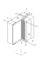
- FIG. 2 is a perspective view of the first multilayer ceramic capacitor 10.
- the dimension in the X-axis direction of the first multilayer ceramic capacitor 10, that is, the length, is expressed as L[10]
- the dimension in the Y-axis direction, that is, the width is expressed as W[10].
- the dimension in the Z-axis direction, that is, the height is expressed as T[10].
- the dimension in the X-axis direction of the first external electrode 14, that is, the length, is expressed as L[14].
- the dimension in the X-axis direction of the second external electrode 15, that is, the length, is expressed as L[15].
- the gap along the X-axis direction between the first external electrode 14 and the second external electrode 15 is expressed as G[10]. Note that the ceramic body 11, which will be described later, is exposed between the first external electrode 14 and the second external electrode 15.
- the second multilayer ceramic capacitor 30 is also represented in the same manner. However, the length directions of the first multilayer ceramic capacitor 10 and the second multilayer ceramic capacitor 30 are perpendicular to each other. Therefore, in the second multilayer ceramic capacitor 30, the Y-axis dimension is the length dimension and is represented as L[30], and the X-axis dimension is the width dimension and is represented as W[30]. The Z-axis dimension is the height dimension and is represented as T[30], similar to the first multilayer ceramic capacitor 10.
- the Y-axis dimension of the first external electrode 34 that is, the length, is represented as L[34].
- the Y-axis dimension of the second external electrode 35 that is, the length, is represented as L[35].
- the gap along the Y-axis direction between the first external electrode 34 and the second external electrode 35 is represented as G[30]. Note that the ceramic body 31, which will be described later, is exposed between the first external electrode 34 and the second external electrode 35.
- FIG. 3(A) to FIG. 3(D) are four-sided views of the first multilayer ceramic capacitor 10.
- the first multilayer ceramic capacitor 10 and the second multilayer ceramic capacitor 30 are identical and have roughly the same external shape.
- FIG. 2 and FIG. 3(A) to FIG. 3(D) show reference numbers indicating the components of both.
- the descriptions regarding the X-axis, Y-axis, and Z-axis are based on the state in which the first multilayer ceramic capacitor 10 is mounted on the substrate 1. In other words, the description is based on a coordinate system set on the substrate.
- the first multilayer ceramic capacitor 10 comprises a ceramic body 11, a first external electrode 14, and a second external electrode 15.
- the ceramic body 11 is configured as a hexahedron having first and second main surfaces M11, M12 perpendicular to the Z axis, first and second end faces E11, E12 perpendicular to the X axis, and first and second side faces S11, S12 perpendicular to the Y axis.
- hexahedron refers to any shape that is substantially hexahedral, and for example, the ridges connecting the faces of the ceramic body 11 may be rounded.
- the main surfaces M11, M12, end surfaces E11, E12, and side surfaces S11, S12 of the ceramic body 11 are all configured as flat surfaces.
- the flat surfaces do not have to be strictly planar as long as they are recognized as flat when viewed overall, and include, for example, surfaces with minute irregularities on the surface or gently curved shapes that exist within a specified range.
- the first multilayer ceramic capacitor 10 is a tall type with a height T[10] that is 1.3 times or more larger than the width W[10].
- the capacitance is increased by increasing the height T[10]. It is preferable that the height T[10] is 1.5 times or more larger than the width W[10].
- the height T[10] can be, for example, 1.6 times or 1.7 times the width W[10], or an even higher ratio. This allows the capacitance of the first multilayer ceramic capacitor 10 to be further increased.
- the condition for height T[10] is defined by the ratio to width W[10], but the condition for height T[10] may be set based on the relationship with length L[10] instead of width W[10].
- the first multilayer ceramic capacitor 10 may be a tall type in which height T[10] is 1.3 times or more larger than length W[10]. Also, height T[10] may be 1.5 times or more larger than length L[10].
- the dimension of the ceramic body 11 in the X-axis direction only needs to be larger than the dimension in the Y-axis direction, and may be smaller than the dimension in the Z-axis direction.
- the dimensions of the ceramic body 11 in the three axial directions can be determined arbitrarily within a range that satisfies the above conditions.
- the length L[10] can be 0.2 mm or more and 1.2 mm or less, and the width W[10] can be 0.1 mm or more and 0.7 mm or less.
- the height T[10] can be 0.15 mm or more and 1.0 mm or less.
- the height T[10], width W[10], and length L[10] are all the maximum dimensions in each direction of the first multilayer ceramic capacitor 10.
- the first external electrode 14 has a first surface portion 14a covering the end face E11 of the ceramic body 11.
- the first external electrode 14 has a second surface portion 14b extending from the first surface portion 14a to the side surface S11, and a third surface portion 14c extending to the side surface S12.
- the first external electrode 14 has a fourth surface portion 14d extending from the first surface portion 14a to the main surface M11, and a fifth surface portion 14e extending to the main surface M12.
- the second external electrode 15 has a first surface portion 15a covering the end face E12 of the ceramic body 11.
- the second external electrode 15 has a second surface portion 15b extending from the first surface portion 15a to the side surface S11, and a third surface portion 15c extending to the side surface S12.
- the second external electrode 15 has a fourth surface portion 15d extending from the first surface portion 15a to the main surface M11, and a fifth surface portion 15e extending to the main surface M12.
- the second surface portions 14b, 15b, the third surface portions 14c, 15c, the fourth surface portions 14d, 15d, and the fifth surface portions 14e, 15e correspond to the extension portions.
- the cross sections of the external electrodes 14 and 15 parallel to the X-Z plane and the cross sections parallel to the X-Y plane are both U-shaped.
- the shapes of the external electrodes 14 and 15 are not limited to the examples shown in the drawings.
- the external electrodes 14, 15 contain a metal material as a main component.
- metal materials constituting the external electrodes 14, 15 include copper (Cu), nickel (Ni), tin (Sn), palladium (Pd), platinum (Pt), silver (Ag), gold (Au), and alloys of these.
- the main component refers to the component with the highest content.
- Figure 4 is a cross-sectional view of the first multilayer ceramic capacitor 10 taken along line A1-A1 in Figure 2.
- Figure 5(A) is a cross-sectional view of the first multilayer ceramic capacitor 10 taken along line A2-A2 in Figure 2.
- Figure 5(B) is a cross-sectional view of the first multilayer ceramic capacitor 10 taken along line A3-A3 in Figure 2. Note that the second external electrode 15 is omitted in Figure 5(B).
- the ceramic body 11 has a laminated portion 20 and a pair of margin portions 18.
- the laminated portion 20 has a capacitance forming portion 16 and a pair of cover portions 17.
- the capacitance forming portion 16 includes a plurality of first and second internal electrodes 12, 13 that are laminated alternately with a plurality of ceramic layers 19 along the Z-axis direction.
- the first internal electrode 12, the second internal electrode 13, and the ceramic layers 19 are each configured in a sheet shape extending along the X-Y plane. Note that the number of layers of the first and second internal electrodes 12, 13 in each figure does not represent the actual number of layers.
- the first and second internal electrodes 12, 13 are alternately arranged along the Z-axis direction so as to face each other in the Z-axis direction.
- the first and second internal electrodes 12, 13 face each other in the Z-axis direction in the central facing region in the X-axis direction and the Y-axis direction.
- the first internal electrode 12 corresponds to the first group, is drawn out from the facing region to one end face E11, and is connected to the first external electrode 14.
- the second internal electrode 13 corresponds to the second group, is drawn out from the facing region to the other end face E12, and is connected to the second external electrode 15.
- the first and second internal electrodes 12, 13 contain a metal material as a main component.
- the metal material is typically nickel (Ni), and other metals include copper (Cu), palladium (Pd), platinum (Pt), silver (Ag), gold (Au), and alloys thereof.
- the metal material forming the internal electrodes 12, 13 may contain a low-melting point metal as an additive element, which has a melting point lower than that of the main component nickel (Ni).
- Such low-melting point metals include, for example, tin (Sn), zinc (Zn), aluminum (Al), gallium (Ga), and germanium (Ge).
- the internal electrodes 12, 13 may contain at least one of these low-melting point metals. By adding such a low-melting point metal, it is possible to improve the sintering property inside the ceramic body 11 and improve the insulation between the internal electrodes 12, 13.
- a dielectric ceramic having a high dielectric constant is used in order to increase the electrostatic capacitance of each ceramic layer 19 between the first and second internal electrodes 12, 13.
- the dielectric ceramic having a high dielectric constant include materials having a perovskite structure containing barium (Ba) and titanium (Ti), such as barium titanate (BaTiO 3 ).
- the dielectric ceramic may be a composition system such as strontium titanate (SrTiO 3 ), calcium titanate (CaTiO 3 ), magnesium titanate (MgTiO 3 ), calcium zirconate (CaZrO 3 ), calcium titanate zirconate (Ca(Zr,Ti)O 3 ), barium calcium titanate zirconate ((Ba,Ca)(Zr,Ti)O 3 ), barium zirconate (BaZrO 3 ), titanium oxide (TiO 2 ), etc.
- a low melting point metal may be added to the dielectric ceramic.
- the content of the low melting point metal and the effect of adding the low melting point metal are as described above, so a detailed description thereof will be omitted here.
- the pair of cover parts 17 cover the capacitance forming part 16 from both sides in the Z-axis direction, which is the stacking direction.
- the cover part 17 is sometimes called a protective layer in the height direction.
- the cover part 17 is composed of, for example, a laminate of ceramic sheets extending along the XY plane. From the viewpoint of suppressing internal stress, etc., it is preferable that the dielectric ceramic that composes the cover part 17 has the same composition as the ceramic layer 19.
- the pair of margin portions 18 are formed along the Z-axis direction and cover the laminated portion 20 from the Y-axis direction.
- the margin portions 18 are sometimes referred to as width-wise protective layers.
- the margin portions 18 are attached to the surfaces of the laminated portion 20 perpendicular to the Y-axis.
- the margin portions 18 are formed from ceramic sheets and configured in a sheet shape extending along the X-Z plane. From the standpoint of suppressing internal stress, etc., it is preferable that the dielectric ceramics that make up the margin portions 18 have the same composition as the ceramic layers 19.
- the second multilayer ceramic capacitor 30 is the same as the first multilayer ceramic capacitor 10. Therefore, the above description of the first multilayer ceramic capacitor 10 generally applies to the description of the second multilayer ceramic capacitor 30.
- the X-axis, Y-axis, and Z-axis in the above description of the first multilayer ceramic capacitor 10 are based on the state in which the first multilayer ceramic capacitor 10 is mounted on the substrate 1. In other words, the description is based on a coordinate system set on the substrate. Therefore, in the description of the second multilayer ceramic capacitor 30, the X-axis is replaced with the Y-axis.
- the second multilayer ceramic capacitor 30 includes a ceramic body 31, a first external electrode 34, and a second external electrode 35.
- the ceramic body 31 is configured as a hexahedron having first and second main surfaces M31, M32 perpendicular to the Z axis, first and second end faces E31, E32 perpendicular to the Y axis, and first and second side surfaces S31, S32 perpendicular to the X axis.
- the ceramic body 31 has a laminated portion and a pair of margin portions.
- the laminated portion has a capacitance forming portion and a pair of cover portions 17.
- the capacitance forming portion includes a plurality of first and second internal electrodes that are laminated alternately with a plurality of ceramic layers along the Z-axis direction.
- Each of the components of the second multilayer ceramic capacitor 30 is the same as each of the components of the first multilayer ceramic capacitor 10 with the same names, and therefore detailed descriptions thereof will be omitted here.
- the first multilayer ceramic capacitor 10 is mounted on the substrate 1 with its length direction aligned with the X-axis direction of the substrate 1.
- the second multilayer ceramic capacitor 30 is mounted on the substrate 1 with its length direction aligned with the Y-axis direction of the substrate 1.
- the second multilayer ceramic capacitor 30 is mounted so that the first external electrode 34 overlaps the region Ar.
- a gap S1 is provided between the second external electrode 15 of the first multilayer ceramic capacitor 10 and the first external electrode 34 of the second multilayer ceramic capacitor 30.
- the gap S1 is the shortest distance along the X-axis direction of the substrate 1 between the second external electrode 15 of the first multilayer ceramic capacitor 10 and the first external electrode 34 of the second multilayer ceramic capacitor 30. No other components are mounted between the first multilayer ceramic capacitor 10 and the second multilayer ceramic capacitor 30. Therefore, from the viewpoint of high-density mounting, it is preferable that the gap S1 be 0.3 mm or less, more preferably 0.2 mm or less.
- a gap S2 is set between the first external electrode 14 and the second external electrode 15 of the first multilayer ceramic capacitor 10 and the second external electrode 35 of the second multilayer ceramic capacitor 30.
- the gap S2 is set to be greater than 0.5 times the height T[10] of the first multilayer ceramic capacitor 10.
- the gap S2 can be set taking into consideration the type of tilt that may occur in the first multilayer ceramic capacitor 10 and the second multilayer ceramic capacitor 30.
- the first multilayer ceramic capacitor 10 may be tilted in the Y-axis direction, i.e., in the width direction, as shown in FIG. 1A.
- the upper edge of the first multilayer ceramic capacitor 10 is tilted so as to approach the second external electrode 35 of the second multilayer ceramic capacitor 30.
- the maximum tilt angle is 30°.
- the interval S2 is set to be greater than 0.2 mm when T[10] is 0.4 mm, and greater than 0.3 mm when T[10] is 0.6 mm. Also, when T[10] is 0.8 mm, the interval S2 is set to be greater than 0.4 mm. As described above, in this embodiment, it is required to avoid contact between the second external electrode 15 of the first multilayer ceramic capacitor 10 and the first external electrode 34 and the second external electrode 35 of the second multilayer ceramic capacitor 30. If an appropriate interval S2 is not set and the first multilayer ceramic capacitor 10 tilts to the right in FIG. 1B and the second multilayer ceramic capacitor 30 tilts downward in FIG. 1B, the above-mentioned contact may occur.
- an appropriate interval S2 is set. Therefore, even if both multilayer ceramic capacitors are tilted, contact between the second external electrode 15 of the first multilayer ceramic capacitor 10 and the first external electrode 34 and second external electrode 35 of the second multilayer ceramic capacitor 30 is avoided.
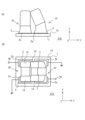
- FIG. 6(A) shows the positional relationship between the first multilayer ceramic capacitor 10 and the second multilayer ceramic capacitor 30 of the first embodiment.
- the distance S2 between the second external electrode 15 of the first multilayer ceramic capacitor 10 and the second external electrode 35 of the second multilayer ceramic capacitor 30 is greater than 0.5 ⁇ T[10].
- FIG. 6B is an explanatory diagram showing the positional relationship between the first multilayer ceramic capacitor 10 and the second multilayer ceramic capacitor 30 in the first modified example of the first embodiment.
- the left-right position of the second multilayer ceramic capacitor 30 in FIG. 6A is a position where the inner edge of the first external electrode 34 of the second multilayer ceramic capacitor 30 roughly coincides with the right edge of the region Ar.
- the second multilayer ceramic capacitor 30 may be disposed at a position where the first external electrode 34 of the second multilayer ceramic capacitor 30 is relatively moved within a range where the first external electrode 34 of the second multilayer ceramic capacitor 30 overlaps with the region Ar, as indicated by an arrow 6a in FIG. 6B.
- the distance between the second external electrode 15 of the first multilayer ceramic capacitor 10 and the second external electrode 35 of the second multilayer ceramic capacitor 30 is equal to or larger than the distance S2 shown in FIG. 6A, and contact between the two is avoided.
- FIG. 6C is an explanatory diagram showing the positional relationship between the first multilayer ceramic capacitor 10 and the second multilayer ceramic capacitor 40 in the second modified example of the first embodiment.
- the second multilayer ceramic capacitor 40 is adopted instead of the second multilayer ceramic capacitor 30.
- the second multilayer ceramic capacitor 40 includes a first external electrode 44 and a second external electrode 45, but is longer than the second multilayer ceramic capacitor 30.
- the first external electrode 44 in the second modified example is moved in the direction indicated by the arrow 6b compared to the first external electrode 34 shown in FIG. 6A, and is accommodated within the region Ar.
- the length of the second multilayer ceramic capacitor 40 is increased to ensure a space S between the second external electrode 15 and the second external electrode 45 of the first multilayer ceramic capacitor 10.
- FIG. 6D is an explanatory diagram showing the positional relationship between the first multilayer ceramic capacitor 10 and the second multilayer ceramic capacitor 40' in the third modified example of the first embodiment.
- a second multilayer ceramic capacitor 40' is used instead of the second multilayer ceramic capacitor 30.
- the second multilayer ceramic capacitor 40' includes a first external electrode 44' and a second external electrode 45', but is longer than the second multilayer ceramic capacitor 30.
- the second multilayer ceramic capacitor 40' is also longer than the second multilayer ceramic capacitor 40 of the second modified example. This prevents the occurrence of a short circuit.
- the first external electrode 44' of the third modified example has been moved further in the direction indicated by the arrow 6c compared to the first external electrode 44 shown in FIG. 6(C), and its outer edge is located to the left of the left edge of the region Ar.
- the length of the second multilayer ceramic capacitor 40' is increased to ensure a gap S between the second external electrode 15 of the first multilayer ceramic capacitor 10 and the second external electrode 45', thereby avoiding the occurrence of a short circuit.
- the spacing S2 is ensured by increasing the length of the second multilayer ceramic capacitor, but the spacing S2 may also be ensured by shortening the length of the external electrode.
- the height T[10] of the first multilayer ceramic capacitor 10 and the height T[30] of the second multilayer ceramic capacitor 30 can be set large.
- the heights of the second multilayer ceramic capacitor 40 of the third modified example and the second multilayer ceramic capacitor 40' of the fourth modified example can be set large.
- the first multilayer ceramic capacitor 10 and the second multilayer ceramic capacitor 30 are the same, but they do not necessarily have to be the same.
- a circuit board 120 of the second embodiment includes a first multilayer ceramic capacitor 10, a second multilayer ceramic capacitor 30, and an electronic component 70 that is flip-mounted.
- two second multilayer ceramic capacitors 30 are provided.
- the two second multilayer ceramic capacitors 30 are arranged in a line in the length direction.
- the electronic component 70 is disposed on the side of the first multilayer ceramic capacitor 10 in the width direction (Y-axis direction) and in a region along the width direction (X-axis direction) of the second multilayer ceramic capacitor 30.
- the electronic component 70 is disposed adjacent to the first multilayer ceramic capacitor 10 and the second multilayer ceramic capacitor 30.
- the electronic component 70 is covered with an insulating coating. Therefore, even if the first multilayer ceramic capacitor 10 or the second multilayer ceramic capacitor 30 is tilted toward the electronic component 70 located on its side, a short circuit will not occur between the first multilayer ceramic capacitor 10 or the second multilayer ceramic capacitor 30 and the electronic component 70.
- the distance S3 between the first multilayer ceramic capacitor 10 and the electronic component 70, and the distance S4 between the second multilayer ceramic capacitor 30 and the electronic component 70 can be narrowed.
- the height of the first multilayer ceramic capacitor 10 and the height of the second multilayer ceramic capacitor 30 can be set large. From the viewpoint of high-density mounting, it is preferable that the distances S3 and S4 are 0.3 mm or less, and more preferably 0.2 mm or less.
- the circuit board 130 of the third embodiment includes electronic components 71, 72, and 73, as well as the first multilayer ceramic capacitor 10 and the second multilayer ceramic capacitor 30.
- the circuit board 130 of the third embodiment is common to the second embodiment in that it includes two second multilayer ceramic capacitors 30 arranged in a line in the length direction.
- the electronic component 71 is provided instead of the electronic component 70 of the second embodiment.
- the electronic component 72 is disposed in a region separated from the first multilayer ceramic capacitor 10 and one second multilayer ceramic capacitor 30 with respect to the electronic component 71, that is, in a region on the upper left side of the electronic component 71 in FIG. 7C.
- the electronic component 73 is disposed in a region separated from the electronic component 71 by the first multilayer ceramic capacitor 10, that is, in a region on the left side of the first multilayer ceramic capacitor 10 in FIG. 7C.
- the electronic components 71, 72, and 73 are covered with an insulating coating, similar to the electronic component 70 of the embodiment. Therefore, even if the first multilayer ceramic capacitor 10 or the second multilayer ceramic capacitor 30 is tilted toward the electronic component 71, electronic component 72, and electronic component 73 located on its respective side, no short circuit will occur between the first multilayer ceramic capacitor 10 or the second multilayer ceramic capacitor 30 and the electronic components 71, 72, and 73.
- the distance S5 between the external electrode of the second multilayer ceramic capacitor 30 located on the left side and the electronic component 72, and the distance S6 between the two second multilayer ceramic capacitors 30 and the electronic component 71 can be narrowed.
- the distance S7 between the first multilayer ceramic capacitor 10 and the electronic component 71, the distance S8 between the first multilayer ceramic capacitor 10 and the electronic component 73, and the distance S9 between the first multilayer ceramic capacitor 10 and the electronic component 72 can be narrowed.
- the height of the first multilayer ceramic capacitor 10 and the height of the second multilayer ceramic capacitor 30 can be set large.
- the spacings S6 to S9 are 0.3 mm or less, and more preferably 0.2 mm or less, similar to the spacings S3 and S4 in the second embodiment.
- a fourth embodiment will be described with reference to Figures 8 and 9.
- a first multilayer ceramic capacitor 50 is provided instead of the first multilayer ceramic capacitor 10 of the first embodiment.
- the second multilayer ceramic capacitor 30 is also changed to a multilayer ceramic capacitor similar to the first multilayer ceramic capacitor 50.
- the first multilayer ceramic capacitor 50 will be mainly described.
- FIG. 8 is a cross-sectional view of the first multilayer ceramic capacitor 50 taken along a line corresponding to the A1-A1 line in FIG. 2. In other words, it is a cross-sectional view equivalent to the A1-A1 line cross-sectional view of the first multilayer ceramic capacitor 10 of the first embodiment.
- FIG. 9(A) is a cross-sectional view of the first multilayer ceramic capacitor 50 taken along a line corresponding to the A2-A2 line in FIG. 2. In other words, it is a cross-sectional view equivalent to the A2-A2 line cross-sectional view of the first multilayer ceramic capacitor 10 of the first embodiment.
- FIG. 9(A) is a cross-sectional view of the first multilayer ceramic capacitor 50 taken along a line corresponding to the A2-A2 line in FIG. 2. In other words, it is a cross-sectional view equivalent to the A2-A2 line cross-sectional view of the first multilayer ceramic capacitor 10 of the first embodiment.
- FIG. 9(B) is a cross-sectional view of the first multilayer ceramic capacitor 50 taken along a line corresponding to the A3-A3 line in FIG. 2. In other words, it is a cross-sectional view equivalent to the A3-A3 line cross-sectional view of the first multilayer ceramic capacitor 10 of the first embodiment. Note that the second external electrode 55 is omitted in FIG. 9(B).
- the external shape of the first multilayer ceramic capacitor 50 is generally the same as that of the first multilayer ceramic capacitor 10 of the first embodiment. That is, the first multilayer ceramic capacitor 50 includes a ceramic body 51, a first external electrode 54, and a second external electrode 55.
- the first external electrode 54 includes a first surface portion 54a, a second surface portion (not shown), a third surface portion (not shown), a fourth surface portion 54d, and a fifth surface portion 54e.
- the second external electrode 55 includes a first surface portion 55a, a second surface portion (not shown), a third surface portion (not shown), a fourth surface portion 55d, and a fifth surface portion 55e.
- the first multilayer ceramic capacitor 50 includes a first main surface M51, a first side surface S51, and the like. These components are common to the corresponding parts of the first multilayer ceramic capacitor 10 of the first embodiment, and therefore detailed description thereof will be omitted here.
- the length, width, and height of the first multilayer ceramic capacitor 50 are not shown, but are represented as length L[50], width W[50], and height T[50], respectively, similar to the first multilayer ceramic capacitor 10 of the first embodiment.
- the first multilayer ceramic capacitor 50 is a tall type in which the height T[50] is 1.3 times or more larger than the width W[50]. This is also similar to the first multilayer ceramic capacitor 10 of the first embodiment.
- the ceramic body 51 has a laminated portion 56 and a pair of cover portions 57.
- the laminated portion 56 has a capacitance forming portion 60 and a pair of margin portions 58.
- the capacitance forming portion 60 includes a plurality of first and second internal electrodes 52, 53 that are alternately laminated with a plurality of ceramic layers 59 along the Y-axis direction.
- the internal electrodes 52, 53 and the ceramic layers 59 are each configured in a sheet shape extending along the X-Z plane.
- the internal electrodes 52, 53 are laminated along the Y-axis direction and face each other in a direction parallel to the mounting surface 1a, so that the bonding area between each first internal electrode 52 and the first external electrode 54 and the bonding area between each second internal electrode 53 and the second external electrode 55 can be made large. This suppresses a decrease in capacitance due to poor contact, so-called capacitance loss. Note that the number of layers of the first and second internal electrodes 52, 53 in each figure does not represent the actual number of layers.
- the internal electrodes 52, 53 are alternately arranged along the Y-axis direction so as to face each other in the Y-axis direction.
- the internal electrodes 52, 53 face each other in the Y-axis direction in the central facing region in the X-axis direction and the Z-axis direction.
- the first internal electrode 52 corresponds to the first group, is drawn from the facing region to one end face E51, and is connected to the first external electrode 54.
- the second internal electrode 53 corresponds to the second group, is drawn from the facing region to the other end face E52, and is connected to the second external electrode 55.
- the internal electrodes 52, 53 contain a metal material as a main component.
- the metal material is typically nickel (Ni), but other examples include copper (Cu), palladium (Pd), platinum (Pt), silver (Ag), gold (Au), and alloys thereof.
- the internal electrodes 52, 53 can contain a low melting point metal, similar to the internal electrodes 12, 13 in the first embodiment.
- a dielectric ceramic having a high dielectric constant is used in order to increase the electrostatic capacitance of each ceramic layer 59 between the internal electrodes 52, 53.
- a dielectric ceramic having a high dielectric constant is a material having a perovskite structure containing barium (Ba) and titanium (Ti), such as barium titanate (BaTiO 3 ).
- the dielectric ceramic may be a composition system such as strontium titanate ( SrTiO3 ), calcium titanate ( CaTiO3 ), magnesium titanate ( MgTiO3 ), calcium zirconate (CaZrO3), calcium titanate zirconate (Ca(Zr,Ti) O3 ), barium calcium titanate zirconate ((Ba,Ca)(Zr,Ti) O3 ), barium zirconate ( BaZrO3 ), titanium oxide ( TiO2 ), etc.
- a low melting point metal can be added to the dielectric ceramic as in the first embodiment.
- the pair of cover parts 57 are formed along the Y-axis direction and cover the laminate part 56 from the Z-axis direction.
- the cover parts 57 are sometimes referred to as a protective layer in the height direction.
- the cover parts 57 are attached to the surface of the laminate part 56 perpendicular to the Z-axis.
- the cover parts 57 are composed of, for example, a laminate of ceramic sheets extending along the X-Y plane. From the viewpoint of suppressing internal stress, etc., it is preferable that the dielectric ceramics constituting the cover parts 57 have the same composition as the ceramic layer 59.
- the pair of margin portions 58 are formed along the Z-axis direction and cover the capacitance forming portion 60 from the Y-axis direction.
- the margin portions 58 are sometimes referred to as width-wise protective layers.
- the margin portions 58 are formed, for example, from a ceramic sheet and configured in a sheet shape extending along the X-Z plane. From the standpoint of suppressing internal stress, it is preferable that the dielectric ceramic that constitutes the margin portions 58 has the same composition as the ceramic layer 59.
- the second multilayer ceramic capacitor used in place of the second multilayer ceramic capacitor 30 is the same as the first multilayer ceramic capacitor 50, so a detailed description of it will be omitted.
- the first multilayer ceramic capacitor 50 and the second multilayer ceramic capacitor are mounted on the substrate 1 in the same manner as the first multilayer ceramic capacitor 10 and the second multilayer ceramic capacitor 30 of the first embodiment shown in Figures 1(A) and 1(B).
- electrostriction may occur in the first multilayer ceramic capacitor 50.
- the electrostriction is a cause of so-called acoustic noise.
- the lamination direction of the internal electrodes 52, 53 in the first multilayer ceramic capacitor 50 is the width direction, which is perpendicular to the mounting direction, i.e., the Z-axis direction. This suppresses acoustic noise in the first multilayer ceramic capacitor 50. Acoustic noise caused by electrostriction is similarly suppressed in the second multilayer ceramic capacitor.
- the first multilayer ceramic capacitor 50 and the second multilayer ceramic capacitor are identical, but one of them may be replaced with, for example, the first multilayer ceramic capacitor 10 of the first embodiment.
- the fifth embodiment differs from the first embodiment in the following points.
- FIG. 10 a partially disassembled state of a ceramic body included in the first multilayer ceramic capacitor 10 is shown.
- the fifth embodiment includes a first internal electrode 12 and a second internal electrode 13, as in the first embodiment, but the shapes of the electrodes are different. Since the other parts are the same as those of the first embodiment, the fifth embodiment will be described below with appropriate reference to the drawings for explaining the first embodiment. In addition, in the description, the same reference numbers will be used for components common to the first embodiment.
- the first internal electrode 12 included in the first group is connected to the first external electrode 14, and the second internal electrode 13 included in the second group is connected to the second external electrode 15.
- the first internal electrode 12 of this embodiment has a connection end 12a that is connected to the first external electrode 14, and an open end 12b located on the opposite side of the connection end 12a.
- a notch 12a2 is provided in the connection end 12a to form a narrow portion 12a1.
- the width of the narrow portion 12a1 is narrower than the width dimension on the side closer to the open end 12b than the connection end 12a.
- the dimension of the narrow portion 12a1 in the direction along the width direction of the first multilayer ceramic capacitor 10 is smaller than the dimension of the open end 12b in the direction along the width direction of the first multilayer ceramic capacitor 10. This is also true for the second multilayer ceramic capacitor 30.
- the second internal electrode 13 of this embodiment has a connection end 13a connected to the second external electrode 15, and an open end 13b located opposite the connection end 13a.
- a notch 13a2 is provided in the connection end 13a to form a narrow portion 13a1.
- the width of the narrow portion 13a1 is narrower than the width dimension on the side closer to the open end 13b than the connection end 13a.
- the dimension of the narrow portion 13a1 in the direction along the width direction of the first multilayer ceramic capacitor 10 is smaller than the dimension of the open end 13b in the direction along the width direction of the first multilayer ceramic capacitor 10. This is also true for the second multilayer ceramic capacitor 30.
- the external shapes of the first multilayer ceramic capacitor 10 and the second multilayer ceramic capacitor 30 in the first embodiment, as well as the dimensional relationship and positional relationship between them, are maintained. Therefore, in the fifth embodiment, as in the first embodiment, short circuits between the first multilayer ceramic capacitor 10 and the second multilayer ceramic capacitor 30 are suppressed.
- the first multilayer ceramic capacitor and the second multilayer ceramic capacitor are the same.
- the internal electrodes of both ceramic capacitors have a narrow portion.
- the fifth embodiment maintains the basic form of the first embodiment while changing the shapes of the internal electrodes 12, 13.
- this modified example maintains the basic form of the fourth embodiment while changing the shapes of the internal electrodes 52, 53.
- the first multilayer ceramic capacitor 80 corresponds to the first multilayer ceramic capacitor 50 in the fourth embodiment.
- a multilayer ceramic capacitor similar to the first multilayer ceramic capacitor 80 is used for the second multilayer ceramic capacitor.
- the modified embodiment has a first internal electrode 52 and a second internal electrode 53, similar to the fourth embodiment, but the shapes are different. Note that there are no other differences from the fourth embodiment, so in the following explanation, the modified embodiment of the fifth embodiment will be explained with appropriate reference to the drawings for explaining the fourth embodiment. In addition, in the explanation, the same reference numbers will be used for components that are common to the fourth embodiment.
- the first internal electrode 52 included in the first group is connected to the first external electrode 54. Also, as shown in FIG. 9(A), the second internal electrode 53 included in the second group is connected to the second external electrode 55.
- the first internal electrode 52 of this modified example has a connection end 52a connected to the first external electrode 54, and an open end 52b located on the opposite side of the connection end 52a.
- a notch 52a2 is provided in the connection end 52a to form a narrow portion 52a1.
- the width of the narrow portion 52a1 is narrower than the width dimension on the side closer to the open end 52b than the connection end 52a.
- the dimension of the narrow portion 52a1 in the height direction of the first multilayer ceramic capacitor 80 is smaller than the dimension of the open end 52b in the height direction of the first multilayer ceramic capacitor 80.
- the width dimension of the first internal electrode 52 is the dimension along the Z-axis direction.
- the second internal electrode 53 of this modified example has a connection end 53a connected to the second external electrode 55, and an open end 53b located opposite the connection end 53a.
- a notch 53a2 is provided in the connection end 53a to form a narrow portion 53a1.
- the width of the narrow portion 53a1 is narrower than the width dimension on the side closer to the open end 53b than the connection end 53a.
- the dimension of the narrow portion 53a1 in the height direction of the first multilayer ceramic capacitor 80 is smaller than the dimension of the open end 53b in the height direction of the first multilayer ceramic capacitor 80.
- the width dimension of the second internal electrode 53 is also a dimension along the Z-axis direction.
- the first multilayer ceramic capacitor and the second multilayer ceramic capacitor are the same.
- the internal electrodes of both ceramic capacitors have a narrow portion.
- This specification also discloses a variety of multilayer ceramic capacitors with different internal electrode lamination directions and shapes. These multilayer ceramic capacitors can be used in appropriate combinations.
- the comparative example has a configuration in which the first multilayer ceramic capacitor 10 and the second multilayer ceramic capacitor 30 are arranged along the Y-axis direction. At this time, the positions of the first multilayer ceramic capacitor 10 and the second multilayer ceramic capacitor 30 along the X-axis direction are the same. In other words, the first external electrode 14 of the first multilayer ceramic capacitor 10 and the first external electrode 34 of the second multilayer ceramic capacitor 30 are adjacent to each other along the Y-axis direction. The second external electrode 15 of the first multilayer ceramic capacitor 10 and the second external electrode 35 of the second multilayer ceramic capacitor 30 are adjacent to each other along the Y-axis direction. A space S is provided between the first external electrode 14 and the first external electrode 34, and between the second external electrode 15 and the second external electrode 35.
- First multilayer ceramic capacitor 10 Length L[10]: 0.6 mm, width W[10]: 0.3 mm, height T[10]: 0.4 mm
- Second multilayer ceramic capacitor 30 It is the same as the first laminated ceramic, and the dimensions are also the same.
- Spacing S2 0.3 mm
- T[10]/W[10] in pattern 1 is approximately 1.33, which satisfies the condition of the first multilayer ceramic capacitor 10 of the first embodiment that T[10] is 1.3 times or more W[10].
- the second multilayer ceramic capacitor 30 similarly satisfies the condition.
- First multilayer ceramic capacitor 10 Length L[10]: 0.4 mm, width W[10]: 0.2 mm, height T[10]: 0.3 mm
- Second multilayer ceramic capacitor 30 Same as pattern 1.
- Spacing S1 Same as pattern 1.
- Spacing S2 0.2 mm.
- T[10]/W[10] in pattern 2 is 1.5, which satisfies the condition of the first multilayer ceramic capacitor 10 that T[10] is 1.3 times or more, and even 1.5 times or more, of W[10].
- the second multilayer ceramic capacitor 30 satisfies the condition of the second multilayer ceramic capacitor 30 of the first embodiment that T[30] is 1.3 times or more, and even more, than W[30].
- First multilayer ceramic capacitor 10 Length L[10]: 0.6 mm, width W[10]: 0.3 mm, height T[10]: 0.5 mm
- Second multilayer ceramic capacitor 30 Same as pattern 1.
- Spacing S1 Same as pattern 1.
- Spacing S2 Same as pattern 1.
- T[10]/W[10] in pattern 3 is approximately 1.67, which satisfies the condition of the first multilayer ceramic capacitor 10 that T[10] is 1.3 times or more, and even 1.5 times or more, of W[10].
- the second multilayer ceramic capacitor 30 satisfies the condition of the second multilayer ceramic capacitor 30 of the first embodiment that T[30] is 1.3 times or more, and even more than W[30].
- First multilayer ceramic capacitor 10 Length L[10]: 1.0 mm, width W[10]: 0.5 mm, height T[10]: 0.7 mm
- Second multilayer ceramic capacitor 30 Same as pattern 1.
- Spacing S1 Same as pattern 1.
- Spacing S2 0.5mm
- T[10]/W[10] in pattern 4 is approximately 1.4, which satisfies the condition of the first multilayer ceramic capacitor 10 that T[10] is 1.3 times or more than W[10].
- the second multilayer ceramic capacitor 30 satisfies the condition of the second multilayer ceramic capacitor 30 of the first embodiment that T[30] is 1.3 times or more than W[30].
- First multilayer ceramic capacitor 10 Length L[10]: 1.0 mm, width W[10]: 0.5 mm, height T[10]: 0.8 mm
- Second multilayer ceramic capacitor 30 It is the same as the first laminated ceramic, and the dimensions are also the same.
- Spacing S1 Same as pattern 1.
- Spacing S2 0.5mm
- T[10]/W[10] in pattern 4 is 1.6, which satisfies the condition of the first multilayer ceramic capacitor 10 that T[10] is 1.3 times or more, and even 1.5 times or more, than W[10].
- the second multilayer ceramic capacitor 30 satisfies the condition of the second multilayer ceramic capacitor 30 of the first embodiment that T[30] is 1.3 times or more than W[30].
- T[10]/W[10] in the comparative example is approximately 1.33, which satisfies the condition of the first multilayer ceramic capacitor 10 of the first embodiment that T[10] is 1.3 times or more W[10].
- Test Method A predetermined number of samples were prepared for each of the patterns 1 to 5 of the embodiment and the comparative example. From these samples, samples in which the first multilayer ceramic capacitor 10 and the second multilayer ceramic capacitor 30 were determined to be tilted were extracted. A voltage was applied between the first terminal 4a and the second terminal 4b for testing of the extracted samples, and the presence or absence of a short circuit was confirmed.
- the occurrence of a short circuit can be suppressed even when T[10] is 1.3 times or more than W[10], and even when T[10] is 1.5 times or more than W[10].
- the external shape of the first multilayer ceramic capacitor 10 and the dimensional and positional relationships with the second multilayer ceramic capacitor 30 in the first embodiment are maintained in the second to fifth embodiments and their modified examples. Therefore, it is believed that the occurrence of short circuits can be similarly suppressed in all of the embodiments.
- a multilayer ceramic capacitor has been described as an example of a multilayer ceramic electronic component, but the present invention is not limited to this.
- the configuration of each of the above embodiments can also be applied to other multilayer ceramic electronic components, such as varistors and thermistors.
Landscapes
- Engineering & Computer Science (AREA)
- Power Engineering (AREA)
- Microelectronics & Electronic Packaging (AREA)
- Manufacturing & Machinery (AREA)
- Fixed Capacitors And Capacitor Manufacturing Machines (AREA)
- Ceramic Capacitors (AREA)
Priority Applications (2)
| Application Number | Priority Date | Filing Date | Title |
|---|---|---|---|
| JP2025505308A JPWO2024185702A1 (https=) | 2023-03-03 | 2024-03-01 | |
| CN202480016321.2A CN120917877A (zh) | 2023-03-03 | 2024-03-01 | 电路板 |
Applications Claiming Priority (2)
| Application Number | Priority Date | Filing Date | Title |
|---|---|---|---|
| JP2023-032770 | 2023-03-03 | ||
| JP2023032770 | 2023-03-03 |
Publications (1)
| Publication Number | Publication Date |
|---|---|
| WO2024185702A1 true WO2024185702A1 (ja) | 2024-09-12 |
Family
ID=92675069
Family Applications (1)
| Application Number | Title | Priority Date | Filing Date |
|---|---|---|---|
| PCT/JP2024/007847 Ceased WO2024185702A1 (ja) | 2023-03-03 | 2024-03-01 | 回路基板 |
Country Status (3)
| Country | Link |
|---|---|
| JP (1) | JPWO2024185702A1 (https=) |
| CN (1) | CN120917877A (https=) |
| WO (1) | WO2024185702A1 (https=) |
Citations (6)
| Publication number | Priority date | Publication date | Assignee | Title |
|---|---|---|---|---|
| JP2004179531A (ja) * | 2002-11-28 | 2004-06-24 | Murata Mfg Co Ltd | 積層セラミック電子部品及びその製造方法 |
| JP2005050962A (ja) * | 2003-07-31 | 2005-02-24 | Taiyo Yuden Co Ltd | コンデンサ実装構造,コンデンサ実装基板及びコンデンサ実装用配線基板 |
| JP2020031152A (ja) * | 2018-08-23 | 2020-02-27 | 太陽誘電株式会社 | 積層セラミック電子部品、積層セラミック電子部品実装基板及び積層セラミック電子部品包装体並びに積層セラミック電子部品の製造方法 |
| JP2021044533A (ja) * | 2019-09-10 | 2021-03-18 | サムソン エレクトロ−メカニックス カンパニーリミテッド. | 積層セラミックキャパシタ及びその製造方法 |
| JP2022008697A (ja) * | 2013-04-17 | 2022-01-14 | サムソン エレクトロ-メカニックス カンパニーリミテッド. | 積層セラミック電子部品及びその実装基板 |
| JP2022067608A (ja) * | 2020-10-20 | 2022-05-06 | サムソン エレクトロ-メカニックス カンパニーリミテッド. | 積層型電子部品 |
-
2024
- 2024-03-01 CN CN202480016321.2A patent/CN120917877A/zh active Pending
- 2024-03-01 JP JP2025505308A patent/JPWO2024185702A1/ja active Pending
- 2024-03-01 WO PCT/JP2024/007847 patent/WO2024185702A1/ja not_active Ceased
Patent Citations (6)
| Publication number | Priority date | Publication date | Assignee | Title |
|---|---|---|---|---|
| JP2004179531A (ja) * | 2002-11-28 | 2004-06-24 | Murata Mfg Co Ltd | 積層セラミック電子部品及びその製造方法 |
| JP2005050962A (ja) * | 2003-07-31 | 2005-02-24 | Taiyo Yuden Co Ltd | コンデンサ実装構造,コンデンサ実装基板及びコンデンサ実装用配線基板 |
| JP2022008697A (ja) * | 2013-04-17 | 2022-01-14 | サムソン エレクトロ-メカニックス カンパニーリミテッド. | 積層セラミック電子部品及びその実装基板 |
| JP2020031152A (ja) * | 2018-08-23 | 2020-02-27 | 太陽誘電株式会社 | 積層セラミック電子部品、積層セラミック電子部品実装基板及び積層セラミック電子部品包装体並びに積層セラミック電子部品の製造方法 |
| JP2021044533A (ja) * | 2019-09-10 | 2021-03-18 | サムソン エレクトロ−メカニックス カンパニーリミテッド. | 積層セラミックキャパシタ及びその製造方法 |
| JP2022067608A (ja) * | 2020-10-20 | 2022-05-06 | サムソン エレクトロ-メカニックス カンパニーリミテッド. | 積層型電子部品 |
Also Published As
| Publication number | Publication date |
|---|---|
| JPWO2024185702A1 (https=) | 2024-09-12 |
| CN120917877A (zh) | 2025-11-07 |
Similar Documents
| Publication | Publication Date | Title |
|---|---|---|
| JP5899699B2 (ja) | 積層型コンデンサ | |
| KR102938187B1 (ko) | 적층형 전자 부품 | |
| JP7494436B2 (ja) | 積層セラミック電子部品及びその製造方法 | |
| JP2023122205A (ja) | 積層セラミックコンデンサ及び回路基板 | |
| JP4513855B2 (ja) | 積層コンデンサ | |
| US11024461B2 (en) | Multi-layer ceramic electronic component having external electrode with base film and electrically conductive thin film | |
| JP5042892B2 (ja) | 貫通コンデンサ | |
| JP2023143584A (ja) | 積層型電子部品 | |
| WO2024185702A1 (ja) | 回路基板 | |
| TWI837232B (zh) | 積層陶瓷電子零件及電路基板 | |
| WO2024143220A1 (ja) | 回路基板 | |
| WO2024177077A1 (ja) | 回路基板 | |
| KR20170065444A (ko) | 적층 세라믹 전자부품 | |
| WO2024185766A1 (ja) | 回路基板 | |
| WO2024185777A1 (ja) | 回路基板 | |
| WO2024009997A1 (ja) | 積層セラミックコンデンサ、包装体、及び回路基板 | |
| JP7359595B2 (ja) | 積層セラミックコンデンサ、回路基板及び積層セラミックコンデンサの製造方法 | |
| US20250301574A1 (en) | Circuit board | |
| JP7696723B2 (ja) | 積層コンデンサ | |
| US11955287B2 (en) | Multilayer electronic component | |
| KR20240140622A (ko) | 전자 부품 | |
| JP2024101984A (ja) | コンデンサ、コンデンサ装置および通信装置 | |
| JP2018093165A (ja) | 積層セラミックコンデンサ | |
| WO2024071083A1 (ja) | 回路基板 | |
| JP2025088116A (ja) | 積層セラミック電子部品 |
Legal Events
| Date | Code | Title | Description |
|---|---|---|---|
| 121 | Ep: the epo has been informed by wipo that ep was designated in this application |
Ref document number: 24767070 Country of ref document: EP Kind code of ref document: A1 |
|
| ENP | Entry into the national phase |
Ref document number: 2025505308 Country of ref document: JP Kind code of ref document: A |
|
| WWE | Wipo information: entry into national phase |
Ref document number: 2025505308 Country of ref document: JP |
|
| WWE | Wipo information: entry into national phase |
Ref document number: 202480016321.2 Country of ref document: CN |
|
| NENP | Non-entry into the national phase |
Ref country code: DE |
|
| WWP | Wipo information: published in national office |
Ref document number: 202480016321.2 Country of ref document: CN |
|
| 122 | Ep: pct application non-entry in european phase |
Ref document number: 24767070 Country of ref document: EP Kind code of ref document: A1 |