WO2024185420A1 - 半導体装置、半導体装置アッセンブリ、および車両 - Google Patents
半導体装置、半導体装置アッセンブリ、および車両 Download PDFInfo
- Publication number
- WO2024185420A1 WO2024185420A1 PCT/JP2024/004975 JP2024004975W WO2024185420A1 WO 2024185420 A1 WO2024185420 A1 WO 2024185420A1 JP 2024004975 W JP2024004975 W JP 2024004975W WO 2024185420 A1 WO2024185420 A1 WO 2024185420A1
- Authority
- WO
- WIPO (PCT)
- Prior art keywords
- semiconductor element
- semiconductor
- center
- distance
- semiconductor elements
- Prior art date
- Legal status (The legal status is an assumption and is not a legal conclusion. Google has not performed a legal analysis and makes no representation as to the accuracy of the status listed.)
- Ceased
Links
Images










Classifications
-
- H—ELECTRICITY
- H10—SEMICONDUCTOR DEVICES; ELECTRIC SOLID-STATE DEVICES NOT OTHERWISE PROVIDED FOR
- H10W—GENERIC PACKAGES, INTERCONNECTIONS, CONNECTORS OR OTHER CONSTRUCTIONAL DETAILS OF DEVICES COVERED BY CLASS H10
- H10W90/00—Package configurations
- H10W90/10—Configurations of laterally-adjacent chips
-
- H—ELECTRICITY
- H10—SEMICONDUCTOR DEVICES; ELECTRIC SOLID-STATE DEVICES NOT OTHERWISE PROVIDED FOR
- H10W—GENERIC PACKAGES, INTERCONNECTIONS, CONNECTORS OR OTHER CONSTRUCTIONAL DETAILS OF DEVICES COVERED BY CLASS H10
- H10W40/00—Arrangements for thermal protection or thermal control
- H10W40/20—Arrangements for cooling
- H10W40/25—Arrangements for cooling characterised by their materials
- H10W40/255—Arrangements for cooling characterised by their materials having a laminate or multilayered structure, e.g. direct bond copper [DBC] ceramic substrates
-
- H—ELECTRICITY
- H10—SEMICONDUCTOR DEVICES; ELECTRIC SOLID-STATE DEVICES NOT OTHERWISE PROVIDED FOR
- H10W—GENERIC PACKAGES, INTERCONNECTIONS, CONNECTORS OR OTHER CONSTRUCTIONAL DETAILS OF DEVICES COVERED BY CLASS H10
- H10W74/00—Encapsulations, e.g. protective coatings
- H10W74/10—Encapsulations, e.g. protective coatings characterised by their shape or disposition
- H10W74/111—Encapsulations, e.g. protective coatings characterised by their shape or disposition the semiconductor body being completely enclosed
-
- H—ELECTRICITY
- H10—SEMICONDUCTOR DEVICES; ELECTRIC SOLID-STATE DEVICES NOT OTHERWISE PROVIDED FOR
- H10W—GENERIC PACKAGES, INTERCONNECTIONS, CONNECTORS OR OTHER CONSTRUCTIONAL DETAILS OF DEVICES COVERED BY CLASS H10
- H10W90/00—Package configurations
-
- H—ELECTRICITY
- H10—SEMICONDUCTOR DEVICES; ELECTRIC SOLID-STATE DEVICES NOT OTHERWISE PROVIDED FOR
- H10W—GENERIC PACKAGES, INTERCONNECTIONS, CONNECTORS OR OTHER CONSTRUCTIONAL DETAILS OF DEVICES COVERED BY CLASS H10
- H10W40/00—Arrangements for thermal protection or thermal control
-
- H—ELECTRICITY
- H10—SEMICONDUCTOR DEVICES; ELECTRIC SOLID-STATE DEVICES NOT OTHERWISE PROVIDED FOR
- H10W—GENERIC PACKAGES, INTERCONNECTIONS, CONNECTORS OR OTHER CONSTRUCTIONAL DETAILS OF DEVICES COVERED BY CLASS H10
- H10W40/00—Arrangements for thermal protection or thermal control
- H10W40/40—Arrangements for thermal protection or thermal control involving heat exchange by flowing fluids
- H10W40/47—Arrangements for thermal protection or thermal control involving heat exchange by flowing fluids by flowing liquids, e.g. forced water cooling
-
- H—ELECTRICITY
- H10—SEMICONDUCTOR DEVICES; ELECTRIC SOLID-STATE DEVICES NOT OTHERWISE PROVIDED FOR
- H10W—GENERIC PACKAGES, INTERCONNECTIONS, CONNECTORS OR OTHER CONSTRUCTIONAL DETAILS OF DEVICES COVERED BY CLASS H10
- H10W40/00—Arrangements for thermal protection or thermal control
- H10W40/70—Fillings or auxiliary members in containers or in encapsulations for thermal protection or control
- H10W40/77—Auxiliary members characterised by their shape
- H10W40/778—Auxiliary members characterised by their shape in encapsulations
-
- H—ELECTRICITY
- H10—SEMICONDUCTOR DEVICES; ELECTRIC SOLID-STATE DEVICES NOT OTHERWISE PROVIDED FOR
- H10W—GENERIC PACKAGES, INTERCONNECTIONS, CONNECTORS OR OTHER CONSTRUCTIONAL DETAILS OF DEVICES COVERED BY CLASS H10
- H10W70/00—Package substrates; Interposers; Redistribution layers [RDL]
- H10W70/40—Leadframes
- H10W70/411—Chip-supporting parts, e.g. die pads
-
- H—ELECTRICITY
- H10—SEMICONDUCTOR DEVICES; ELECTRIC SOLID-STATE DEVICES NOT OTHERWISE PROVIDED FOR
- H10W—GENERIC PACKAGES, INTERCONNECTIONS, CONNECTORS OR OTHER CONSTRUCTIONAL DETAILS OF DEVICES COVERED BY CLASS H10
- H10W70/00—Package substrates; Interposers; Redistribution layers [RDL]
- H10W70/40—Leadframes
- H10W70/421—Shapes or dispositions
- H10W70/442—Shapes or dispositions of multiple leadframes in a single chip
-
- H—ELECTRICITY
- H10—SEMICONDUCTOR DEVICES; ELECTRIC SOLID-STATE DEVICES NOT OTHERWISE PROVIDED FOR
- H10W—GENERIC PACKAGES, INTERCONNECTIONS, CONNECTORS OR OTHER CONSTRUCTIONAL DETAILS OF DEVICES COVERED BY CLASS H10
- H10W70/00—Package substrates; Interposers; Redistribution layers [RDL]
- H10W70/40—Leadframes
- H10W70/464—Additional interconnections in combination with leadframes
- H10W70/465—Bumps or wires
-
- H—ELECTRICITY
- H10—SEMICONDUCTOR DEVICES; ELECTRIC SOLID-STATE DEVICES NOT OTHERWISE PROVIDED FOR
- H10W—GENERIC PACKAGES, INTERCONNECTIONS, CONNECTORS OR OTHER CONSTRUCTIONAL DETAILS OF DEVICES COVERED BY CLASS H10
- H10W90/00—Package configurations
- H10W90/701—Package configurations characterised by the relative positions of pads or connectors relative to package parts
- H10W90/751—Package configurations characterised by the relative positions of pads or connectors relative to package parts of bond wires
- H10W90/754—Package configurations characterised by the relative positions of pads or connectors relative to package parts of bond wires between a chip and a stacked insulating package substrate, interposer or RDL
-
- H—ELECTRICITY
- H10—SEMICONDUCTOR DEVICES; ELECTRIC SOLID-STATE DEVICES NOT OTHERWISE PROVIDED FOR
- H10W—GENERIC PACKAGES, INTERCONNECTIONS, CONNECTORS OR OTHER CONSTRUCTIONAL DETAILS OF DEVICES COVERED BY CLASS H10
- H10W90/00—Package configurations
- H10W90/701—Package configurations characterised by the relative positions of pads or connectors relative to package parts
- H10W90/751—Package configurations characterised by the relative positions of pads or connectors relative to package parts of bond wires
- H10W90/756—Package configurations characterised by the relative positions of pads or connectors relative to package parts of bond wires between a chip and a stacked lead frame, conducting package substrate or heat sink
-
- H—ELECTRICITY
- H10—SEMICONDUCTOR DEVICES; ELECTRIC SOLID-STATE DEVICES NOT OTHERWISE PROVIDED FOR
- H10W—GENERIC PACKAGES, INTERCONNECTIONS, CONNECTORS OR OTHER CONSTRUCTIONAL DETAILS OF DEVICES COVERED BY CLASS H10
- H10W90/00—Package configurations
- H10W90/811—Multiple chips on leadframes
Definitions
- This disclosure relates to semiconductor devices, semiconductor device assemblies, and vehicles.
- Patent Document 1 discloses a conventional semiconductor device.
- MOSFETs Metal Oxide Semiconductor Field Effect Transistors
- IGBTs Insulated Gate Bipolar Transistors
- Such semiconductor devices are mounted in all kinds of electronic devices, from industrial equipment to home appliances, information terminals, and automotive equipment.
- Patent Document 1 discloses a conventional semiconductor device.
- multiple semiconductor chips semiconductor chips are arranged on a lead (conductive portion). The multiple semiconductor chips are aligned linearly at predetermined intervals along the x-direction, which is perpendicular to the thickness direction of the lead.
- One of the objectives of this disclosure is to provide a semiconductor device that is an improvement over conventional semiconductor devices.
- one of the objectives of this disclosure is to provide a semiconductor device that is suitable for suppressing interference between heat generated by multiple semiconductor elements and reducing thermal resistance.
- the semiconductor device provided by the first aspect of the present disclosure includes a conductive portion having a first main surface facing one side in a thickness direction and a first back surface facing the opposite side to the first main surface, four or more semiconductor elements arranged on the first main surface, and a sealing resin covering the semiconductor elements and at least a part of the conductive portion.
- the semiconductor elements are arranged side by side in a first direction perpendicular to the thickness direction.
- the semiconductor elements include a first semiconductor element and a second semiconductor element close to the center in the first direction, and a first distance that is the distance between the center of the first semiconductor element and the center of the second semiconductor element is greater than a second distance that is the distance between the center of either the first semiconductor element or the second semiconductor element and the center of another semiconductor element adjacent to either the first semiconductor element or the second semiconductor element in the first direction.
- the multiple semiconductor elements include a third semiconductor element close to the center in the first direction, a fourth semiconductor element adjacent to one side of the third semiconductor element in the first direction, and a fifth semiconductor element adjacent to the other side of the third semiconductor element in the first direction, and each of a third distance that is the distance between the center of the third semiconductor element and the center of the fourth semiconductor element and a fourth distance that is the distance between the center of the third semiconductor element and the center of the fifth semiconductor element is greater than a fifth distance that is the distance between the center of either the fourth semiconductor element or the fifth semiconductor element and the center of the other semiconductor element adjacent to either the fourth semiconductor element or the fifth semiconductor element in the first direction.
- the semiconductor device assembly provided by the second aspect of the present disclosure includes a semiconductor device according to the first aspect of the present disclosure, a cooler, and a cooling means for cooling the cooler.
- the second back surface of the support is exposed from the sealing resin, and the cooler has a portion that contacts the second back surface.
- the vehicle provided by the third aspect of the present disclosure is equipped with a power conversion device configured to include a semiconductor device according to the first aspect of the present disclosure.
- the above configuration makes it possible to suppress thermal interference caused by multiple semiconductor elements and reduce thermal resistance.
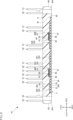
- FIG. 1 is a perspective view showing a semiconductor device according to a first embodiment of the present disclosure.
- FIG. 2 is a plan view showing the semiconductor device according to the first embodiment of the present disclosure.
- FIG. 3 is a plan view showing the semiconductor device according to the first embodiment of the present disclosure.
- FIG. 4 is a bottom view showing the semiconductor device according to the first embodiment of the present disclosure.
- FIG. 5 is a cross-sectional view taken along line VV in FIG.
- FIG. 6 is a cross-sectional view taken along line VI-VI in FIG.
- FIG. 7 is a cross-sectional view taken along line VII-VII in FIG.
- FIG. 8 is a cross-sectional view taken along line VIII-VIII in FIG.
- FIG. 5 is a cross-sectional view taken along line VV in FIG.
- FIG. 6 is a cross-sectional view taken along line VI-VI in FIG.
- FIG. 7 is a cross-sectional view taken along line VII-VII in FIG.
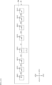
- FIG. 9 is a schematic plan view showing the arrangement of a plurality of semiconductor elements in the semiconductor device according to the first embodiment of the present disclosure.
- FIG. 10 is a schematic diagram of a vehicle including the semiconductor device according to the first embodiment of the present disclosure.
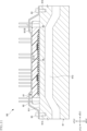
- FIG. 11 is a cross-sectional view showing a first example of a semiconductor device assembly including the semiconductor device according to the first embodiment of the present disclosure.
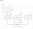
- FIG. 12 is a block diagram showing the configuration of the semiconductor device assembly shown in FIG.
- FIG. 13 is a cross-sectional view showing a second example of a semiconductor device assembly including the semiconductor device according to the first embodiment of the present disclosure.
- FIG. 14 is a schematic plan view showing a modified example of the arrangement of a plurality of semiconductor elements.
- FIG. 15 is a schematic plan view showing a modified example of the arrangement of a plurality of semiconductor elements.
- FIG. 16 is a schematic plan view showing a modified example of the arrangement of a plurality of semiconductor elements.
- FIG. 17 is a schematic plan view showing a modified example of the arrangement of a plurality of semiconductor elements.
- FIG. 18 is a plan view showing a semiconductor device according to the second embodiment of the present disclosure.
- FIG. 19 is a cross-sectional view taken along line XIX-XIX in FIG.
- FIG. 20 is a cross-sectional view taken along line XX-XX in FIG.
- FIG. 21 is a cross-sectional view taken along line XXI-XXI in FIG.
- FIG. 22 is a schematic plan view showing an arrangement of a plurality of semiconductor elements in a semiconductor device according to a second embodiment of the present disclosure.
- FIG. 23 is a plan view showing a semiconductor device according to a third embodiment of the present disclosure.
- FIG. 24 is a schematic plan view showing an arrangement of a plurality of semiconductor elements in a semiconductor device according to a third embodiment of the present disclosure.
- FIG. 25 is a schematic diagram of a vehicle including a semiconductor device according to a third embodiment of the present disclosure.
- FIG. 26 is a schematic plan view showing an arrangement of a plurality of semiconductor elements in a semiconductor device according to a first modification of the third embodiment.
- FIG. 27 is a schematic plan view showing an arrangement of a plurality of semiconductor elements in a semiconductor device according to a first modification of the third embodiment.
- FIG. 28 is a schematic plan view showing an arrangement of a plurality of semiconductor elements in a semiconductor device according to a first modification of the third embodiment.
- FIG. 29 is a schematic plan view showing an arrangement of a plurality of semiconductor elements in a semiconductor device according to a first modification of the third embodiment.
- an object A is formed on an object B" and “an object A is formed on an object B” include “an object A is formed directly on an object B” and “an object A is formed on an object B with another object interposed between the object A and the object B” unless otherwise specified.
- an object A is disposed on an object B” and “an object A is disposed on an object B” include “an object A is disposed directly on an object B” and “an object A is disposed on an object B with another object interposed between the object A and the object B" unless otherwise specified.
- an object A is located on an object B includes “an object A is located on an object B in contact with an object B” and “an object A is located on an object B with another object interposed between the object A and the object B” unless otherwise specified.
- an object A overlaps an object B when viewed in a certain direction includes “an object A overlaps the entire object B” and “an object A overlaps a part of an object B.”
- a surface A faces in direction B is not limited to the case where the angle of surface A with respect to direction B is 90 degrees, but also includes the case where surface A is tilted with respect to direction B.
- First embodiment: 1 to 8 show a semiconductor device according to a first embodiment of the present disclosure.
- a semiconductor device A1 of this embodiment includes a plurality of leads 1, a plurality of leads 2, a support 3, a support conductor 32, a plurality of semiconductor elements 4, a wiring portion 5, a thermistor 6, a plurality of wires 71, 72, 73, and 74, and a sealing resin 8.
- FIG. 1 is a perspective view of the semiconductor device A1.
- FIG. 2 is a plan view of the semiconductor device A1.
- FIG. 3 is a plan view of the semiconductor device A1, seen through the sealing resin 8.
- FIG. 4 is a bottom view of the semiconductor device A1.
- FIG. 5 is a cross-sectional view taken along line V-V in FIG. 3.
- FIG. 6 is a cross-sectional view taken along line VI-VI in FIG. 3.
- FIG. 7 is a cross-sectional view taken along line VII-VII in FIG. 3.
- FIG. 8 is a cross-sectional view taken along line VIII-VIII in FIG. 3.
- the outline of the sealing resin 8 is shown by an imaginary line (two-dot chain line). Wires 71 are omitted in FIGS. 5 to 8.
- the thickness direction (direction in plan view) of the support 3 is an example of the "thickness direction” of the present disclosure, and is referred to as the "thickness direction z".
- the direction perpendicular to the thickness direction z is an example of the "first direction” of the present disclosure, and is referred to as the "first direction x”.
- the direction perpendicular to both the thickness direction z and the first direction x is an example of the "second direction” of the present disclosure, and is referred to as the "second direction y".
- the left side of the figures is an example of the "one side of the first direction" of the present disclosure, and is referred to as the "x1 side of the first direction x”
- the right side of the figures is an example of the "other side of the first direction” of the present disclosure, and is referred to as the "x2 side of the first direction x”
- the upper side of the figures is an example of the "one side of the second direction” of the present disclosure, and is referred to as the "y1 side of the second direction y”
- the lower side of the figures is an example of the "other side of the second direction” of the present disclosure, and is referred to as the "y2 side of the second direction y".
- the upper side in the figure is an example of “one side in the thickness direction” in this disclosure and is called the “z1 side in the thickness direction z”
- the lower side in the figure is an example of "the other side in the thickness direction” in this disclosure and is called the “z2 side in the thickness direction z.”
- the support 3 and the support conductor 32 support a plurality of semiconductor elements 4.
- the specific configuration of the support 3 is not limited in any way, and is, for example, an AMB (Active Metal Brazing) substrate or a DBC (Direct Bonded Copper) substrate.
- the support 3 is defined as being composed of an insulating substrate 31 and a metal layer 33.
- the support 3 has a second main surface 3a and a second back surface 3b.
- the second main surface 3a faces the z1 side in the thickness direction z.
- the second back surface 3b faces the opposite side to the second main surface 3a (the z2 side in the thickness direction z).
- the AMB substrate or DBC substrate constituting the support 3 includes an insulating substrate 31, a support conductor 32, and a metal layer 33.
- the total thickness (dimension in the thickness direction z) of the insulating substrate 31, the support conductor 32, and the metal layer 33 including the support 3 is not particularly limited, and is, for example, about 0.4 mm to 3.0 mm.
- the insulating substrate 31 is, for example, a ceramic having excellent thermal conductivity. Examples of such ceramics include silicon nitride (SiN) and alumina (Al 2 O 3 ).
- the insulating substrate 31 is not limited to ceramics and may be an insulating resin sheet or the like.
- the shape of the insulating substrate 31 is not particularly limited, and is, for example, rectangular in a plan view. In this embodiment, the insulating substrate 31 is an elongated rectangular shape with the first direction x as the longitudinal direction when viewed in the thickness direction z.
- the insulating substrate 31 has a second main surface 3a.
- the second main surface 3a is a flat surface facing the z1 side in the thickness direction z.
- the thickness of the insulating substrate 31 is not particularly limited, and is, for example, about 0.05 mm to 1.0 mm.
- the support conductor 32 is formed on the second main surface 3a of the insulating substrate 31.
- the constituent material of the support conductor 32 includes, for example, copper (Cu).
- the constituent material may include, for example, aluminum (Al) other than copper.
- the first back surface 32b faces the opposite side to the first main surface 32a (the z2 side in the thickness direction z) and faces the second main surface 3a.
- the thickness of the support conductor 32 is not particularly limited, and is, for example, about 0.1 mm to 1.5 mm.
- the support conductor 32 includes a first conductor portion 321, a second conductor portion 322, a third conductor portion 323, a fourth conductor portion 324, a fifth conductor portion 325, a sixth conductor portion 326, a seventh conductor portion 327, and an eighth conductor portion 328.
- the surfaces of the first conductor portion 321 to the eighth conductor portion 328 may be plated with, for example, silver (Ag).
- the first conductor portion 321 is disposed near the center in the first direction x on the second main surface 3a of the insulating substrate 31.
- the first conductor portion 321 supports one of the multiple semiconductor elements 4.
- the second conductor portion 322 is disposed on the x2 side in the first direction x with respect to the first conductor portion 321, and is adjacent to the first conductor portion 321.
- the second conductor portion 322 supports one of the multiple semiconductor elements 4.
- the third conductor portion is disposed on the x1 side in the first direction x with respect to the first conductor portion 321, and is adjacent to the first conductor portion 321.
- the third conductor portion 323 supports one of the multiple semiconductor elements 4.
- the fourth conductor portion 324 is disposed on the x1 side in the first direction x with respect to the third conductor portion 323, and is adjacent to the third conductor portion 323.
- the fourth conductor portion 324 supports one of the multiple semiconductor elements 4.
- the fifth conductor portion 325 and the sixth conductor portion 326 are disposed near the corners of the insulating substrate 31 on the x2 side in the first direction x and on the y1 side in the second direction y.
- a wire 73 is bonded to the fifth conductor portion 325.
- a wire 72 is bonded to the sixth conductor portion 326.
- the seventh conductor portion 327 and the eighth conductor portion 328 are disposed near the corners of the insulating substrate 31 on the x1 side in the first direction x and on the y1 side in the second direction y.
- the seventh conductor portion 327 and the eighth conductor portion 328 are located on the x1 side in the first direction x with respect to the third conductor portion 323, and on the y1 side in the second direction y with respect to the fourth conductor portion 324.
- a wire 73 is bonded to the seventh conductor portion 327.
- a wire 72 is bonded to the eighth conductor portion 328.
- the support conductor 32 that supports the multiple semiconductor elements 4 corresponds to an example of a "conductive portion" in this disclosure.
- the metal layer 33 is bonded to the lower surface (surface facing the z2 side in the thickness direction z) of the insulating substrate 31.
- the constituent material of the metal layer 33 is the same as the constituent material of the support conductor 32.
- the metal layer 33 has a second back surface 3b.
- the second back surface 3b is a flat surface facing the z2 side in the thickness direction z. In this embodiment, the second back surface 3b is exposed from the sealing resin 8.
- a heat dissipation member for example, a heat sink not shown in the figure can be attached to the second back surface 3b.
- the heat capacity of the structure (for example, an AMB substrate or a DBC substrate) consisting of the support conductor 32 and the support 3 (the insulating substrate 31 and the metal layer 33) is, for example, 0.01 to 15 J/K.
- the thermal resistance of the structure (for example, an AMB substrate or a DBC substrate) consisting of the support conductor 32 and the support 3 is, for example, 0.0003 to 1.5 K/W.
- the wiring portion 5 is formed on the second main surface 3a of the insulating substrate 31.
- the wiring portion 5 is made of a conductive material.
- the conductive material constituting the wiring portion 5 is not particularly limited. Examples of the conductive material of the wiring portion 5 include those containing silver (Ag), copper (Cu), gold (Au), etc. In the following explanation, a case where the wiring portion 5 contains silver will be described as an example.
- the wiring portion 5 may contain copper instead of silver, or may contain gold instead of silver or copper. Alternatively, the wiring portion 5 may contain Ag-Pt or Ag-Pd.
- the method of forming the wiring portion 5 is not limited, and it is formed, for example, by firing a paste containing these metals.
- the thickness of the wiring portion 5 is not particularly limited, and is, for example, about 5 ⁇ m to 30 ⁇ m. The thickness of the wiring portion 5 is smaller than the thickness of the support conductor 32 described above.
- the shape of the wiring portion 5 is not particularly limited.
- the wiring portion 5 includes two wirings 501, for example as shown in FIG. 3.
- the two wirings 501 are arranged near a corner on the x1 side in the first direction x and on the y1 side in the second direction y of the insulating substrate 31.
- the two wirings 501 are spaced apart from each other and arranged side by side in the second direction y.
- Each wiring 501 has a pad portion 502.
- the pad portion 502 is located at the end of the wiring 501 on the x2 side in the first direction x.
- Each terminal of the thermistor 6 is joined to the two pad portions 502.
- the multiple leads 1 are made of a metal and have a higher thermal conductivity than the insulating substrate 31, for example.
- the metal constituting the leads 1 is not particularly limited, and may be, for example, copper, aluminum, iron (Fe), oxygen-free copper, or an alloy thereof (for example, a Cu-Sn alloy, a Cu-Zr alloy, a Cu-Fe alloy, etc.).
- the multiple leads 1 may also be plated with nickel (Ni).
- the multiple leads 1 may be formed, for example, by pressing a metal die against a metal plate, or by patterning a metal plate by etching.
- the method of forming the multiple leads 1 is not limited.
- the thickness of each lead 1 is not particularly limited, and may be, for example, about 0.4 mm to 0.8 mm.
- the leads 1 are spaced apart from each other.
- the multiple leads 1 include lead 11, lead 12, lead 13, lead 14, and lead 15.
- Lead 11, lead 12, lead 13, lead 14, and lead 15 form a conductive path to the semiconductor element 4, and protrude from a side surface (resin side surface 86 described later) of the sealing resin 8 facing the y2 side of the second direction y (the lower side in FIG. 2).
- the lead 11 is disposed on the support conductor 32, and in this embodiment, is disposed on the second conductor portion 322. As shown in FIG. 7, the lead 11 is joined to the second conductor portion 322 via a conductive bonding material 19.
- the conductive bonding material 19 may be any material that can bond the lead 11 to the second conductor portion 322 and electrically connect the lead 11 and the second conductor portion 322.
- the conductive bonding material 19 may be, for example, silver paste, copper paste, solder, or the like.
- the configuration of the lead 11 is not particularly limited. In this embodiment, as shown in Figures 3 and 7, the lead 11 is described by dividing it into a connection end 111, a protruding portion 112, an inclined portion 113, and a parallel portion 114.
- connection end 111 has a rectangular shape in a plan view and is a portion that is joined to the second conductor portion 322.
- the connection end 111 is conductively joined to the end of the second conductor portion 322 on the y2 side in the second direction y via a conductive bonding material 19. It is covered by the inclined portion 113, the parallel portion 114, and the sealing resin 8.
- the inclined portion 113 is connected to the connection end 111 and the parallel portion 114, and is inclined with respect to the connection end 111 and the parallel portion 114.
- the parallel portion 114 is connected to the inclined portion 113 and the protruding portion 112, and is parallel to the connection end 111.
- the protruding portion 112 is connected to the end of the parallel portion 114, and is a portion of the lead 11 that protrudes from the sealing resin 8.
- two protruding portions 112 are provided at an interval in the first direction x.
- Each protruding portion 112 protrudes on the opposite side to the connection end 111 in the second direction y.
- the protrusion 112 is used, for example, to electrically connect the semiconductor device A1 to an external circuit.
- the protrusion 112 is bent in the thickness direction z toward the side facing the second main surface 3a of the insulating substrate 31.
- the lead 12 is disposed on the support conductor 32, and in this embodiment, is disposed on the first conductor portion 321.
- the lead 12 is joined to the first conductor portion 321 via a conductive bonding material.
- the configuration of the lead 12 is not particularly limited. In this embodiment, as shown in FIG. 3, the lead 12 is described by dividing it into a connection end portion 121, a protruding portion 122, an inclined portion 123, and a parallel portion 124.
- connection end 121 has a rectangular shape in a plan view and is a portion that is joined to the first conductor portion 321.
- the connection end 121 is conductively joined to the end of the first conductor portion 321 on the y2 side in the second direction y via a conductive bonding material.
- the inclined portion 123 and the parallel portion 124 are covered with the sealing resin 8.
- the inclined portion 123 is connected to the connection end 121 and the parallel portion 124 and is inclined with respect to the connection end 121 and the parallel portion 124.
- the parallel portion 124 is connected to the inclined portion 123 and the protruding portion 122 and is parallel to the connection end 121.
- a wire 71 is joined to the parallel portion 124.
- the protruding portion 122 is connected to the end of the parallel portion 124 and is a portion of the lead 12 that protrudes from the sealing resin 8.
- the protruding portion 122 protrudes on the opposite side to the connection end 121 in the second direction y.
- the protruding portion 122 is used, for example, to electrically connect the semiconductor device A1 to an external circuit.
- the protrusion 122 is bent in the thickness direction z toward the side facing the second main surface 3a of the insulating substrate 31.
- the lead 13 is disposed on the support conductor 32, and in this embodiment, is disposed on the third conductor portion 323. As shown in FIG. 6, the lead 13 is joined to the third conductor portion 323 via a conductive bonding material 19.
- the configuration of the lead 13 is not particularly limited. In this embodiment, the lead 13 will be described by dividing it into a connection end portion 131, a protruding portion 132, an inclined portion 133, and a parallel portion 134, as shown in FIG. 3 and FIG. 6.
- connection end 131 has a rectangular shape in a plan view and is a portion that is joined to the third conductor portion 323.
- the connection end 131 is conductively joined to the end of the third conductor portion 323 on the y2 side in the second direction y via a conductive bonding material 19.
- the inclined portion 133 and the parallel portion 134 are covered with the sealing resin 8.
- the inclined portion 133 is connected to the connection end 131 and the parallel portion 134 and is inclined with respect to the connection end 131 and the parallel portion 134.
- the parallel portion 134 is connected to the inclined portion 133 and the protruding portion 132 and is parallel to the connection end 131.
- a wire 71 is joined to the parallel portion 134.
- the protruding portion 132 is connected to the end of the parallel portion 134 and is a portion of the lead 13 that protrudes from the sealing resin 8.
- the protruding portion 132 protrudes on the opposite side to the connection end 131 in the second direction y.
- the protruding portion 132 is used, for example, to electrically connect the semiconductor device A1 to an external circuit.
- the protrusion 132 is bent in the thickness direction z toward the side facing the second main surface 3a of the insulating substrate 31.
- the lead 14 is disposed on the support conductor 32, and in this embodiment, is disposed on the fourth conductor portion 324.
- the lead 14 is joined to the fourth conductor portion 324 via a conductive bonding material.
- the configuration of the lead 14 is not particularly limited. In this embodiment, as shown in FIG. 3, the lead 14 is described by dividing it into a connection end portion 141, a protruding portion 142, an inclined portion 143, and a parallel portion 144.
- connection end 141 has a rectangular shape in a plan view and is a portion that is joined to the fourth conductor portion 324.
- the connection end 141 is conductively joined to the end of the fourth conductor portion 324 on the y2 side in the second direction y via a conductive bonding material.
- the inclined portion 143 and the parallel portion 144 are covered with the sealing resin 8.
- the inclined portion 143 is connected to the connection end 141 and the parallel portion 144 and is inclined with respect to the connection end 141 and the parallel portion 144.
- the parallel portion 144 is connected to the inclined portion 143 and the protruding portion 142 and is parallel to the connection end 141.
- a wire 71 is joined to the parallel portion 144.
- the protruding portion 142 is connected to the end of the parallel portion 144 and is a portion of the lead 14 that protrudes from the sealing resin 8.
- the protruding portion 142 protrudes on the opposite side to the connection end 141 in the second direction y.
- the protruding portion 142 is used, for example, to electrically connect the semiconductor device A1 to an external circuit.
- the protrusion 142 is bent in the thickness direction z toward the side facing the second main surface 3a of the insulating substrate 31.
- the lead 15 is not disposed on the support conductor 32, but is supported by the sealing resin 8.
- the lead 15 does not include a portion corresponding to the connection end 131 and the inclined portion 133 of the lead 13. Note that the configuration of the lead 15 is not limited to this. In this embodiment, the lead 15 will be described by dividing it into a protruding portion 152 and a parallel portion 154, as shown in FIG. 3.
- the parallel portion 154 is covered with the sealing resin 8.
- the parallel portion 154 is parallel to the support conductor 32.
- a wire 71 is joined to the parallel portion 154.
- the protruding portion 152 is connected to an end of the parallel portion 154 and is a portion of the lead 15 that protrudes from the sealing resin 8.
- the protruding portion 152 protrudes from the sealing resin 8 on the y2 side in the second direction y.
- the protruding portion 152 is used, for example, to electrically connect the semiconductor device A1 to an external circuit.
- the protruding portion 152 is bent in the thickness direction z toward the side facing the second main surface 3a of the insulating substrate 31.
- the multiple leads 2 are made of a metal and have a higher thermal conductivity than the insulating substrate 31, for example.
- the metal constituting the leads 2 is not particularly limited, and may be, for example, copper, aluminum, iron (Fe), oxygen-free copper, or an alloy thereof (for example, a Cu-Sn alloy, a Cu-Zr alloy, a Cu-Fe alloy, etc.).
- the multiple leads 2 may be plated with nickel (Ni).
- the multiple leads 2 may be formed, for example, by pressing a metal die against a metal plate, or by patterning a metal plate by etching.
- the method of forming the multiple leads 2 is not limited.
- the thickness of each lead 2 is not particularly limited, and may be, for example, about 0.4 mm to 0.8 mm.
- the leads 2 are spaced apart from each other.
- the multiple leads 2 include multiple leads 21, multiple leads 22, and two leads 23.
- Leads 21 and 22 form a conductive path to a source electrode 43 and a gate electrode 44 of the semiconductor element 4, which will be described later, and protrude from a side surface (resin side surface 85, which will be described later) of the sealing resin 8 facing the y1 side of the second direction y (the upper side in FIG. 2).
- the two leads 23 form a conductive path to the thermistor 6, and protrude from a side surface of the sealing resin 8 facing the y1 side of the second direction y.
- the multiple leads 21 are not disposed on the support conductor 32, but are supported by the sealing resin 8.
- the multiple leads 21 are disposed at intervals in the first direction x.
- the configuration of the leads 21 is not particularly limited. In this embodiment, the leads 21 are described by dividing them into a protruding portion 212 and a parallel portion 214, as shown in Figures 3 and 6.
- the parallel portion 214 is covered with the sealing resin 8.
- the parallel portion 214 is parallel to the support conductor 32.
- a wire 73 is joined to the parallel portion 214.
- the protruding portion 212 is connected to an end of the parallel portion 214 and is a portion of the lead 21 that protrudes from the sealing resin 8.
- the protruding portion 212 protrudes from the sealing resin 8 on the y1 side in the second direction y.
- the protruding portion 212 is used, for example, to electrically connect the semiconductor device A1 to an external circuit.
- the protruding portion 212 is bent in the thickness direction z towards the side facing the second main surface 3a of the insulating substrate 31.
- the multiple leads 22 are not disposed on the support conductor 32, but are supported by the sealing resin 8.
- the multiple leads 22 are disposed at intervals in the first direction x.
- Each of the multiple leads 22 is disposed adjacent to one of the multiple leads 21 so as to form a pair.
- the configuration of the leads 22 is not particularly limited. In this embodiment, the leads 22 are described by dividing them into a protruding portion 222 and a parallel portion 224, as shown in Figures 3 and 7.
- the parallel portion 224 is covered with the sealing resin 8.
- the parallel portion 224 is parallel to the support conductor 32.
- a wire 72 is joined to the parallel portion 224.
- the protruding portion 222 is connected to an end of the parallel portion 224 and is a portion of the lead 22 that protrudes from the sealing resin 8.
- the protruding portion 222 protrudes from the sealing resin 8 on the y1 side in the second direction y.
- the protruding portion 222 is used, for example, to electrically connect the semiconductor device A1 to an external circuit.
- the protruding portion 222 is bent in the thickness direction z toward the side facing the second main surface 3a of the insulating substrate 31.
- the two leads 23 are not disposed on the support conductor 32, but are supported by the sealing resin 8.
- the two leads 23 are disposed side by side in the first direction x.
- the configuration of the leads 23 is not particularly limited. In this embodiment, the lead 23 is described by dividing it into a protruding portion 232 and a parallel portion 234, as shown in Figures 3 and 5.
- the parallel portion 234 is covered with the sealing resin 8.
- the parallel portion 234 is parallel to the support conductor 32.
- a wire 74 is joined to the parallel portion 234.
- the protruding portion 232 is connected to an end of the parallel portion 234 and is a portion of the lead 23 that protrudes from the sealing resin 8.
- the protruding portion 232 protrudes from the sealing resin 8 on the y1 side in the second direction y.
- the protruding portion 232 is used, for example, to electrically connect the semiconductor device A1 to an external circuit.
- the protruding portion 232 is bent in the thickness direction z toward the side toward which the second main surface 3a of the insulating substrate 31 faces.
- Each of the multiple semiconductor elements 4 is an electronic component that is the functional center of the semiconductor device A1, and in this embodiment, is a switching element.
- the multiple semiconductor elements 4 are arranged on the first main surface 32a of the support conductor 32. Specifically, four or more multiple semiconductor elements 4 are arranged at a distance from each other, and each of the multiple semiconductor elements 4 is supported by one of the first conductor portion 321 to the fourth conductor portion 324 of the support conductor 32.
- the multiple semiconductor elements 4 include semiconductor elements 40A to 40F. In the illustrated example, six semiconductor elements 40A to 40F are provided, but this is just one example, and the number of semiconductor elements 4 is not limited in any way as long as it is four or more.
- the semiconductor element 4 (each of the semiconductor elements 40A to 40F) is configured to include at least one of a wide band gap semiconductor and an ultra wide band gap semiconductor.
- wide band gap semiconductors include SiC (silicon carbide) and GaN (gallium nitride).
- ultra wide band gap semiconductors include Ga 2 O 3 (gallium oxide) and C (diamond).
- the semiconductor element 4 (each of the semiconductor elements 40A to 40F) is, for example, a MOSFET (SiC MOSFET (metal-oxide-semiconductor field-effect transistor)) made of a SiC (silicon carbide) substrate.
- the semiconductor element 4 may be a MOSFET made of a Si (silicon) substrate instead of a SiC substrate, and may include, for example, an IGBT element. It may also be a MOSFET containing GaN (gallium nitride). The semiconductor element 4 may also be a diode instead of the above-mentioned switching element.
- the semiconductor element 4 is a rectangular plate in plan view, and includes an element main surface 41, an element back surface 42, a source electrode 43, a gate electrode 44, and a drain electrode 45.
- the element main surface 41 and the element back surface 42 face opposite each other in the thickness direction z.
- the element main surface 41 faces the z1 side in the thickness direction z.
- the element back surface 42 faces the z2 side in the thickness direction z.
- the element main surface 41 is provided with a source electrode 43 and a gate electrode 44.
- the element back surface 42 is provided with a drain electrode 45.
- the shapes and arrangements of the source electrode 43, gate electrode 44, and drain electrode 45 are not limited.
- the source electrode 43 is larger than the gate electrode 44 in the thickness direction z.
- the source electrode 43 is composed of two separated regions in the thickness direction z.
- the heat capacity of each semiconductor element 4 is, for example, 0.0001 to 0.5 J/K.
- the thermal resistance of each semiconductor element 4 is, for example, 0.0003 to 1.5 K/W.
- the semiconductor elements 40A, 40B, and 40C are disposed on the second conductor portion 322. As shown in Figures 7 and 8, the semiconductor elements 40A, 40B, and 40C are joined to the second conductor portion 322 by the conductive bonding material 47 with the element back surface 42 facing the second conductor portion 322. As a result, the drain electrodes 45 of the semiconductor elements 40A, 40B, and 40C are conductively connected to the second conductor portion 322 by the conductive bonding material 47.
- the conductive bonding material 47 may be, for example, silver paste, copper paste, or solder.
- the source electrode 43 of the semiconductor element 40A is conductively connected to the lead 12 by the wire 71.
- the source electrode 43 of the semiconductor element 40B is conductively connected to the lead 13 by the wire 71.
- the source electrode 43 of the semiconductor element 40C is conductively connected to the lead 14 by the wire 71.
- the wire 71 is made of, for example, aluminum (Al) or copper (Cu). The material, diameter, and number of the wires 71 are not limited.
- the semiconductor element 40D is disposed on the first conductor portion 321.
- the semiconductor element 40D is joined to the second conductor portion 322 by a conductive bonding material (not shown) with the element back surface 42 facing the first conductor portion 321.
- the drain electrode 45 of the semiconductor element 40D is conductively connected to the first conductor portion 321 by the conductive bonding material.
- the source electrode 43 of the semiconductor element 40D is conductively connected to the lead 15 by the wire 71.
- the semiconductor element 40E is disposed on the third conductor portion 323. As shown in Figures 6 and 8, the semiconductor element 40E is joined to the third conductor portion 323 by a conductive bonding material 47 with the element back surface 42 facing the third conductor portion 323. As a result, the drain electrode 45 of the semiconductor element 40E is conductively connected to the third conductor portion 323 by the conductive bonding material 47. As shown in Figure 3, the source electrode 43 of the semiconductor element 40E is conductively connected to the lead 15 by a wire 71.
- the semiconductor element 40F is disposed on the fourth conductor portion 324. As shown in Figure 5, the semiconductor element 40F is joined to the fourth conductor portion 324 by a conductive bonding material 47 with the element back surface 42 facing the fourth conductor portion 324. As a result, the drain electrode 45 of the semiconductor element 40F is conductively connected to the fourth conductor portion 324 by the conductive bonding material 47. As shown in Figure 3, the source electrode 43 of the semiconductor element 40F is conductively connected to the lead 15 by a wire 71.
- the gate electrode 44 of the semiconductor element 40A is connected to the sixth conductor portion 326 by a wire 72, and the sixth conductor portion 326 is connected to the lead 22 by a wire 72.
- the gate electrode 44 of the semiconductor element 40A is conductively connected to the lead 22 by the wire 72 and the sixth conductor portion 326.
- the lead 22 conductively connected to the gate electrode 44 of the semiconductor element 40A is a terminal (gate terminal) for inputting a drive signal to the semiconductor element 40A.
- the source electrode 43 of the semiconductor element 40A is connected to the fifth conductor portion 325 by a wire 73, and the fifth conductor portion 325 is connected to the lead 21 by a wire 73.
- the source electrode 43 of the semiconductor element 40A is conductively connected to the lead 21 by the wire 73 and the fifth conductor portion 325.
- the lead 22 conductively connected to the source electrode 43 of the semiconductor element 40A is a terminal for detecting a source signal of the semiconductor element 40A (source sense terminal).
- the wires 72 and 73 are made of, for example, gold (Au), silver (Ag), copper (Cu), aluminum (Al), etc. The material, wire diameter, and number of the wires 72 and 73 are not limited.
- the gate electrode 44 of the semiconductor element 40B is conductively connected to the lead 22 by a wire 72.
- the lead 22 conductively connected to the gate electrode 44 of the semiconductor element 40B is the gate terminal of the semiconductor element 40B.
- the source electrode 43 of the semiconductor element 40B is conductively connected to the lead 21 by a wire 73.
- the lead 21 conductively connected to the source electrode 43 of the semiconductor element 40B is the source sense terminal of the semiconductor element 40B.
- the gate electrode 44 of the semiconductor element 40C is conductively connected to the lead 22 by a wire 72.
- the lead 22 conductively connected to the gate electrode 44 of the semiconductor element 40C is the gate terminal of the semiconductor element 40C.
- the source electrode 43 of the semiconductor element 40C is conductively connected to the lead 21 by a wire 73.
- the lead 21 conductively connected to the source electrode 43 of the semiconductor element 40C is the source sense terminal of the semiconductor element 40C.
- the gate electrode 44 of the semiconductor element 40D is conductively connected to the lead 22 by a wire 72.
- the lead 22 conductively connected to the gate electrode 44 of the semiconductor element 40D is the gate terminal of the semiconductor element 40D.
- the source electrode 43 of the semiconductor element 40D is conductively connected to the lead 21 by a wire 73.
- the lead 21 conductively connected to the source electrode 43 of the semiconductor element 40D is the source sense terminal of the semiconductor element 40D.
- the gate electrode 44 of the semiconductor element 40E is conductively connected to the lead 22 by a wire 72.
- the lead 22 conductively connected to the gate electrode 44 of the semiconductor element 40E is the gate terminal of the semiconductor element 40E.
- the source electrode 43 of the semiconductor element 40E is conductively connected to the lead 21 by a wire 73.
- the lead 21 conductively connected to the source electrode 43 of the semiconductor element 40E is the source sense terminal of the semiconductor element 40E.
- the gate electrode 44 of the semiconductor element 40F is conductively connected to the lead 22 by the wire 72.
- one end of the wire 72 is joined to the gate electrode 44 of the semiconductor element 40F, a middle portion is joined to the eighth conductor portion 328, and the other end is joined to the lead 22.
- the lead 22 conductively connected to the gate electrode 44 of the semiconductor element 40F is the gate terminal of the semiconductor element 40F.
- the source electrode 43 of the semiconductor element 40F is conductively connected to the lead 21 by the wire 73.
- one end of the wire 73 is joined to the source electrode 43 of the semiconductor element 40F, a middle portion is joined to the seventh conductor portion 327, and the other end is joined to the lead 21.
- the lead 21 conductively connected to the source electrode 43 of the semiconductor element 40F is the source sense terminal of the semiconductor element 40F.
- the semiconductor device A1 is configured, for example, as a half-bridge type switching circuit.
- lead 12, lead 13, and lead 14 are externally conductively connected, and the semiconductor elements 40A, 40B, and 40C configure the upper arm circuit of the semiconductor device A1, and the semiconductor elements 40D, 40E, and 40F configure the lower arm circuit.
- the semiconductor elements 40A, 40B, and 40C are connected in parallel with each other, and in the lower arm circuit, the semiconductor elements 40D, 40E, and 40F are connected in parallel with each other.
- Each of the semiconductor elements 40A, 40B, and 40C and each of the semiconductor elements 40D, 40E, and 40F are connected in series to configure a bridge layer.
- a DC voltage to be converted into power is input to lead 11 and lead 15.
- Lead 11 is the positive pole (P terminal)
- lead 15 is the negative pole (N terminal).
- AC voltage converted by semiconductor elements 40A-40F is output from leads 12, 13, and 14.
- semiconductor elements 4 are arranged side by side in the first direction x.
- semiconductor element 40A is located at the end on the x2 side of the first direction x
- semiconductor element 40F is located at the end on the x1 side of the first direction x
- semiconductor elements 40A to 40F are arranged in this order from the x2 side of the first direction x toward the x1 side of the first direction x.
- Semiconductor element 40C and semiconductor element 40D are disposed near the center in the first direction x.
- center in the first direction x refers to the center line CL in the first direction x for the multiple semiconductor elements 40A to 40F aligned in the first direction x, and this also applies to the various modified examples described below.
- the number of multiple semiconductor elements 4 semiconductor elements 40A to 40F
- the two semiconductor elements 40C and 40D are disposed near the center in the first direction x of the multiple semiconductor elements 4.
- the semiconductor elements 40A to 40F are not arranged along the first direction x, but include elements that are positioned differently in the second direction y.
- the semiconductor element 40B is located on the y1 side of the semiconductor element 40A adjacent to the x2 side of the first direction x in the second direction y.
- the semiconductor element 40C is located on the y1 side of the second direction y of the semiconductor element 40B adjacent to the x2 side of the first direction x in the second direction y.
- the semiconductor element 40C is also located on the y1 side of the second direction y of the semiconductor element 40D adjacent to the x1 side of the first direction x in the second direction y.
- the semiconductor element 40D is located on the y1 side of the second direction y of the semiconductor element 40E adjacent to the x1 side of the first direction x in the second direction y.
- the semiconductor element 40E is located on the y1 side of the second direction y of the semiconductor element 40F adjacent to the x1 side of the first direction x in the second direction y.
- the semiconductor element 40E is in the same (or approximately the same) position as the semiconductor element 40B in the second direction y.
- the semiconductor element 40F is in the same (or approximately the same) position as the semiconductor element 40A in the second direction y.
- the semiconductor element 40D corresponds to an example of the "first semiconductor element” in this disclosure
- the semiconductor element 40C corresponds to an example of the "second semiconductor element” in this disclosure
- the first conductor section 321 in which the semiconductor element 40D (first semiconductor element) is arranged corresponds to an example of the "first section” in this disclosure
- the second conductor section 322 in which the semiconductor element 40C (second semiconductor element) is arranged corresponds to an example of the "second section" in this disclosure.
- the distance between the centers of adjacent semiconductor elements 4 in the first direction x has the following relationship.
- a first distance D1 which is the distance between the center C1 of semiconductor element 40D closest to the center in the first direction x and the center C2 of semiconductor element 40C, is greater than a second distance D21, which is the distance between the center C1 of semiconductor element 40D and the center C3 of semiconductor element 40E adjacent to semiconductor element 40D in the first direction x.
- the distance (first distance D1) between the center C1 of semiconductor element 40D and the center C2 of semiconductor element 40C is greater than a second distance D22, which is the distance between the center C2 of semiconductor element 40C and the center C4 of semiconductor element 40B adjacent to semiconductor element 40C in the first direction x. Furthermore, in this embodiment, the distance (first distance D1) between the center C1 of semiconductor element 40D and the center C2 of semiconductor element 40C is at least twice the length (length L1) of the side of semiconductor element 4 along the first direction x.
- the distance (first distance D1) between the center C1 of semiconductor element 40D and the center C2 of semiconductor element 40C is greater than a sixth distance D61, which is the distance between the centers C3, C5 of other semiconductor elements 40E and 40F that are adjacent to each other in the first direction x among the multiple semiconductor elements 4.
- the first distance D1 is also greater than a sixth distance D62, which is the distance between the centers C4, C6 of other semiconductor elements 40B and 40A that are adjacent to each other in the first direction x among the multiple semiconductor elements 4.
- the distance (second distance D21) between the center C1 of semiconductor element 40D and the center C3 of semiconductor element 40E is greater than the distance (sixth distance D61) between the centers C3, C5 of other semiconductor elements 40E and 40F that are adjacent to each other in the first direction x.
- the distance (second distance D22) between the center C2 of semiconductor element 40C and the center C4 of semiconductor element 40B is greater than the distance (sixth distance D62) between the centers C4, C6 of other semiconductor elements 40B and 40A that are adjacent to each other in the first direction x.
- the thermistor 6 is a temperature detection element, and is mounted on the second main surface 3a of the insulating substrate 31.
- the thermistor 6 is a resistor whose electrical resistance changes greatly with temperature changes, and the resistance value changes according to the ambient temperature, causing the voltage between its terminals to change.
- the ambient temperature of the thermistor 6 is detected based on the voltage between its terminals.
- the characteristics of the thermistor 6 are not limited.
- the thermistor 6 may be an NTC (negative temperature coefficient) thermistor, a PTC (positive temperature coefficient) thermistor, or a thermistor with other characteristics.
- the thermistor 6 is for detecting the temperature of the semiconductor device A1. As shown in FIG. 3 and FIG. 5, the thermistor 6 is disposed across two pads 502 of the wiring section 5 (wiring 501). The thermistor 6 is bonded to the pads 502 via a conductive bonding material 63.
- the conductive bonding material 63 may be any material that can bond the thermistor 6 to the pads 502 and electrically connect the thermistor 6 and the pads 502.
- the conductive bonding material 63 may be, for example, silver paste, copper paste, solder, or the like.
- One terminal of the thermistor 6 is conductively bonded to one pad 502 via the conductive bonding material 63, and the other terminal of the thermistor 6 is conductively bonded to the other pad 502 via the conductive bonding material 63.
- Each of the two pads 502 is conductively connected to the leads 23 via wires 74.
- the pads 502 (wiring 501) and wires 74 form a conductive path that connects the thermistor 6 to the leads 23.
- the two leads 23 serve as terminals for detecting the temperature of the semiconductor device A1, and output the voltage between the terminals of the thermistor 6.
- the semiconductor device A1 includes an insulating member 62.
- the insulating member 62 is interposed between the second main surface 3a of the insulating substrate 31 and the thermistor 6, and has electrical insulation properties.
- the insulating member 62 is an underfill filled between the second main surface 3a and the thermistor 6 in the thickness direction z.
- the constituent material of the insulating member 62 is not particularly limited, and is, for example, a synthetic resin whose main component is a black epoxy resin.
- the thermistor 6 is disposed near a corner on the x1 side in the first direction x and on the y1 side in the second direction y of the insulating substrate 31.
- the semiconductor device A1 may be provided with another temperature detection element instead of the thermistor 6.
- the other temperature detection element may be a semiconductor temperature sensor.
- the semiconductor temperature sensor is a Si diode or the like that exhibits a large change in forward voltage relative to temperature changes, and detects the ambient temperature based on the voltage between its terminals when a predetermined current is passed through it.
- the semiconductor device A1 may be configured without a temperature detection element such as the thermistor 6.
- the sealing resin 8 covers at least the semiconductor elements 40A-40F, the wiring portion 5, thermistor 6, wires 71-74, a portion of each of the multiple leads 1 and multiple leads 2, and a portion of the support body 3.
- the material that makes up the sealing resin 8 is made of, for example, a black epoxy resin.
- the sealing resin 8 is formed, for example, by molding.
- the sealing resin 8 has a resin main surface 81, a resin back surface 82, and multiple resin side surfaces 83 to 86.
- the resin main surface 81 and the resin back surface 82 are surfaces facing opposite each other in the thickness direction z, and are both flat surfaces perpendicular to the thickness direction z.
- the resin main surface 81 faces the z1 side of the thickness direction z
- the resin back surface 82 faces the z2 side of the thickness direction z.
- the resin back surface 82 is a frame surrounding the second back surface 3b of the support 3 (metal layer 33) in a plan view.
- the second back surface 3b of the support 3 is exposed from the resin back surface 82 of the sealing resin 8, and is, for example, flush with the resin back surface 82.
- the second back surface 3b of the support 3 may protrude toward the z2 side of the thickness direction z beyond the resin back surface 82 of the sealing resin 8.
- Each of the multiple resin side surfaces 83 to 86 is connected to both the resin main surface 81 and the resin back surface 82, and is sandwiched between them in the thickness direction z.
- the resin side surface 83 and the resin side surface 84 are separated in the first direction x.
- the resin side surface 83 faces the x1 side of the first direction x
- the resin side surface 84 faces the x2 side of the first direction x.
- the resin side surface 85 and the resin side surface 86 are separated in the second direction y.
- the resin side surface 85 faces the y1 side of the second direction y
- the resin side surface 86 faces the y2 side of the second direction y.
- each of the multiple leads 2 protrudes from the resin side surface 85.
- a portion of each of the multiple leads 1 protrudes from the resin side surface 86.
- the resin side surface 83 has a recess 831 recessed in the first direction x.
- the resin side surface 84 has a recess 841 recessed in the first direction x.
- the recesses 831 and 841 are used, for example, for fixing the semiconductor device A1 when mounting it.
- each of the resin side surfaces 85 and 86 has multiple recesses recessed in the second direction y.
- FIG. 10 is a schematic diagram of a vehicle B1 equipped with the semiconductor device A1.
- the vehicle B1 is equipped with an AC-DC converter 871, a power receiving device 872, a storage battery 873, a drive system 874, and a DC-DC converter 875.
- the semiconductor device A1 constitutes a part (PFC circuit) of the AC-DC converter 871.
- the AC-DC converter 871 converts the AC power into high-voltage DC power.
- the AC-DC converter 871 supplies the high-voltage DC power to the storage battery 873.
- the power receiving device 872 supplies power to the storage battery 873 by a non-contact charging system, and is supplied with power by electromagnetic induction from a non-contact charger (not shown) installed in a parking lot or the like.
- the power stored in the storage battery 873 is supplied to a drive system 874 consisting of an inverter, an AC motor, and a transmission.
- the drive system 874 drives the vehicle B1.
- the DC-DC conversion device 875 supplies power to electrical components other than those driving the vehicle B1, and is, for example, a step-down DC-DC converter.
- the above AC-DC conversion device 871 is an example of a "power conversion device" of the present disclosure.
- the semiconductor device A1 includes a support conductor 32, four or more semiconductor elements 4 (semiconductor elements 40A to 40F), and a sealing resin 8.
- the semiconductor elements 40A to 40F include a semiconductor element 40D (first semiconductor element) and a semiconductor element 40C (second semiconductor element) that are close to the center in the first direction x.
- the distance (first distance D1) between the center C1 of the semiconductor element 40D and the center C2 of the semiconductor element 40C is greater than the distance (second distance D21) between the center C1 of the semiconductor element 40D and the center C3 of the semiconductor element 40E adjacent to the semiconductor element 40D in the first direction x, and is also greater than the distance (second distance D22) between the center C2 of the semiconductor element 40C and the center C4 of the semiconductor element 40B adjacent to the semiconductor element 40C in the first direction x.
- the center C1 of semiconductor element 40D and the center C2 of semiconductor element 40C are at different positions in the second direction y, which is perpendicular to the first direction x in which the multiple semiconductor elements 40A-40F are arranged.
- heat generated in semiconductor elements 40D and 40C, which are arranged near the center of the multiple semiconductor elements 40A-40F, can be efficiently dissipated to the surroundings, further suppressing thermal interference.
- the centers of the semiconductor elements 4 adjacent to each other in the first direction x are at different positions in the second direction y.
- heat generated in the multiple semiconductor elements 40A-40F can be dissipated to the surroundings more efficiently.
- the distance (first distance D1) between the center C1 of semiconductor element 40D and the center C2 of semiconductor element 40C is at least twice the length (length L1) of the side of semiconductor element 4 along the first direction x.
- the distance (second distance D21) between the center C1 of the semiconductor element 40D and the center C3 of the semiconductor element 40E is greater than the distance (sixth distance D61) between the center C3 of the semiconductor element 40E and the center C5 of the semiconductor element 40F.
- the distance (second distance D22) between the center C2 of the semiconductor element 40C and the center C4 of the semiconductor element 40B is greater than the distance (sixth distance D62) between the center C4 of the semiconductor element 40B and the center C6 of the semiconductor element 40A.
- the support conductor 32 includes a first conductor portion 321 (first portion) and a second conductor portion 322 (second portion) that are separated from each other.
- first semiconductor element first semiconductor element
- second semiconductor element second semiconductor element
- semiconductor element 40B adjacent to semiconductor element 40C
- the center C1 of semiconductor element 40D is located on the y1 side of the second direction y relative to the centers of all of the semiconductor elements 40A, 40B, 40E, and 40F in the second direction y.
- the center C2 of semiconductor element 40C (second semiconductor element) is located on the y1 side of the second direction y relative to the center C1 of semiconductor element 40D.
- Heat generated by the semiconductor elements 40C and 40B arranged on the common second conductor 322 tends to accumulate in the second conductor 322, and the interference between the heat generated by the semiconductor elements 40C and 40B tends to cause the temperature of the second conductor 322 to rise.
- the second conductor 322 on which the semiconductor element 40C is mounted can efficiently dissipate the heat generated by the semiconductor element 40C to the surroundings of the semiconductor element 40C. Therefore, the mutual thermal interference between the semiconductor elements 40D, 40C, and 40B is suppressed, and the thermal resistance of the semiconductor device A1 can be reduced.
- the semiconductor device A1 includes a support 3.
- the first back surface 32b of the support conductor 32 on which multiple semiconductor elements 4 (semiconductor elements 40A to 40F) are mounted is joined to the second main surface 3a of the support 3 (insulating substrate 31).
- the second back surface 3b of the support 3 (metal layer 33) is exposed from the sealing resin 8.
- FIG. 11 and 12 show a first example of a semiconductor device assembly including a semiconductor device A1.
- FIG. 11 is a cross-sectional view of a main part of a semiconductor device assembly B2 of this example.
- Fig. 12 is a block diagram showing the configuration of the semiconductor device assembly B2.
- the semiconductor device assembly B2 includes the semiconductor device A1, a cooler 91, an attachment member 92, a fastening member 93, a control means 94, a cooling means 95, and a heating means 96.
- the cooler 91 is a heat dissipation member for cooling the semiconductor device A1.
- the cooler 91 is made of a metal material with excellent thermal conductivity.
- the material of the cooler 91 is not particularly limited, and may be, for example, aluminum (Al), copper (Cu), or an alloy of these.
- the cooler 91 has an attachment surface 911 and a flow path 912.
- the attachment surface 911 is a flat surface facing the z1 side in the thickness direction z.
- the flow path 912 is a hollow portion formed inside the cooler 91. For example, cooling water as a refrigerant is passed through this flow path 912.
- the semiconductor device A1 is disposed on the attachment surface 911 of the cooler 91.
- the attachment surface 911 faces the second back surface 3b of the support 3 of the semiconductor device A1 and the resin back surface 82 of the sealing resin 8, and is in surface contact with the second back surface 3b and the resin back surface 82.
- the mounting member 92 is for holding the semiconductor device A1 to the cooler 91.
- the mounting member 92 is arranged across the semiconductor device A1 in the second direction y.
- the mounting member 92 is, for example, a leaf spring.
- the mounting member 92 is attached to the cooler 91 by inserting two fastening members 93 into two mounting holes 913 located on both sides of the semiconductor device A1 in the second direction y.
- the two fastening members 93 are, for example, bolts. In the state where the semiconductor device A1 is pressed against the cooler 91 by the spring elastic force of the mounting member 92, the mounting surface 911 of the cooler 91 and the second back surface 3b of the support 3 of the semiconductor device A1 are in close contact with each other.
- the cooler 91 may be configured to include a TIM (Thermal Interface Material) material (not shown).
- the TIM material is made of, for example, heat dissipation grease or a heat dissipation sheet, and is interposed between the mounting surface 911 and the second back surface 3b.
- the TIM material joins the mounting surface 911 and the second back surface 3b, and is sufficiently in contact with both the mounting surface 911 and the second back surface 3b.
- the cooling means 95 cools the cooler 91.
- the cooling means 95 is configured to include, for example, a cooling water supply source (not shown) and a valve that can be switched between open and closed. For example, when the cooling means 95 cools the cooler 91, the valve is opened and the cooling water sent from the cooling water supply source flows through the flow path 912. When cooling the cooler 91 is to be stopped, the valve is closed and the flow of cooling water through the flow path 912 is stopped. Note that the cooling means 95 only needs to be capable of cooling the cooler 91, and the specific configuration of the cooling means 95 is not limited in any way.
- the heating means 96 heats the cooler 91.
- the heating means 96 includes, for example, a heater (not shown) attached to the cooler 91. For example, when the cooler 91 is heated by the heating means 96, the heater is activated. Note that the heating means 96 only needs to be capable of heating the cooler 91, and the specific configuration of the heating means 96 is not limited in any way.
- the control means 94 controls the cooling means 95 and the heating means 96 based on the temperature detected by the thermistor 6 of the semiconductor device A1. For example, when the temperature detected by the thermistor 6 exceeds a predetermined first temperature, the control means 94 operates the cooling means 95 to cool the cooler 91. When the temperature detected by thermistor 6 falls below a predetermined second temperature (a temperature lower than the first temperature), the control means 94 operates the heating means 96 to heat the cooler 91. Note that the specific method of control of the cooling means 95 and the heating means 96 by the control means 94 is not limited in any way.
- the semiconductor device assembly B2 of this example includes the semiconductor device A1, a cooler 91, a cooling means 95 for cooling the cooler 91, and a control means 94.
- the second back surface 3b of the support 3 in the semiconductor device A1 is exposed from the sealing resin 8, and the cooler 91 has a portion (mounting surface 911 or TIM material) that contacts the second back surface 3b of the support 3. With this configuration, it is possible to suppress a temperature rise in the semiconductor device A1.
- the semiconductor device assembly B2 includes a control means 94.
- the control means 94 controls the cooling means 95 based on the temperature detected by the thermistor 6 of the semiconductor device A1. With this configuration, it is possible to prevent an excessive temperature rise of the semiconductor device A1 while monitoring the temperature of the semiconductor device A1, and it is possible to operate the semiconductor device A1 appropriately.
- the semiconductor device assembly B2 includes a heating means 96 for heating the cooler 91, and the control means 94 controls the heating means 96 based on the temperature detected by the thermistor 6.
- Fig. 13 shows a second example of a semiconductor device assembly including the semiconductor device A1.
- Fig. 13 is a cross-sectional view of a main part of a semiconductor device assembly B21 of this example.
- the configuration of the semiconductor device assembly B21 is similar to that of the first example of the semiconductor device assembly B2 shown in Fig. 12 above.
- the semiconductor device assembly B21 includes the semiconductor device A1, a cooler 91, a fastening member 93, a control means 94, a cooling means 95, and a heating means 96.
- the cooler 91, the control means 94, the cooling means 95, and the heating means 96 are similar to those of the semiconductor device assembly B2 described above, and detailed description thereof will be omitted.
- the semiconductor device A1 is disposed on the mounting surface 911 of the cooler 91.
- the mounting surface 911 faces the second back surface 3b of the support 3 of the semiconductor device A1 and the resin back surface 82 of the sealing resin 8, and is in surface contact with at least the second back surface 3b.
- the cooler 91 has two mounting holes 913.
- the two mounting holes 913 are formed at positions corresponding to the recesses 831 and 841 of the semiconductor device A1.
- the semiconductor device A1 is fixed to the cooler 91 by passing two fastening members 93 through the recesses 831 and 841 and through the two mounting holes 913.
- the two fastening members 93 are, for example, bolts.
- the cooler 91 may be configured to include a TIM material (not shown).
- the TIM material is the same as that described above with respect to the first example of the semiconductor device assembly B2, and therefore will not be described here.
- the semiconductor device assembly B2 of this example includes the semiconductor device A1, a cooler 91, cooling means 95 for cooling the cooler 91, and control means 94.
- the second back surface 3b of the support 3 in the semiconductor device A1 is exposed from the sealing resin 8, and the cooler 91 has a portion (mounting surface 911 or TIM material) that contacts the second back surface 3b of the support 3. With this configuration, it is possible to suppress a rise in temperature of the semiconductor device A1.
- the semiconductor device assembly B2 of this example includes the semiconductor device A1, a cooler 91, a cooling means 95 for cooling the cooler 91, and a control means 94.
- the second back surface 3b of the support 3 in the semiconductor device A1 is exposed from the sealing resin 8, and the cooler 91 has a portion (mounting surface 911 or TIM material) that contacts the second back surface 3b of the support 3. With this configuration, it is possible to suppress a rise in temperature of the semiconductor device A1.
- the semiconductor device assembly B21 has the same effects as the semiconductor device assembly B2 described above.
- FIGS. 14 to 17 show modified examples of the arrangement of the semiconductor elements 4.
- Each of FIGS. 14 to 17 is a schematic plan view showing the arrangement of the semiconductor elements 4.
- the configurations other than the semiconductor elements 4 and the supporting conductor 32 supporting them are the same as those of the semiconductor device A1 of the above embodiment, and the description thereof is omitted.
- elements that are the same as or similar to those of the semiconductor device A1 of the above embodiment are given the same reference numerals as those of the above embodiment, and the description is omitted as appropriate.
- the configurations of the respective parts in the modified examples from FIG. 14 onwards can be appropriately combined with each other as long as no technical contradiction occurs.
- the multiple semiconductor elements 4 include five semiconductor elements 40G to 4OK.
- the multiple semiconductor elements 4 (semiconductor elements 40G to 40K) are arranged side by side in the first direction x.
- Semiconductor element 40G is located at the end on the x2 side of the first direction x
- semiconductor element 40K is located at the end on the x1 side of the first direction x
- semiconductor elements 40G to 40K are arranged in this order from the x2 side of the first direction x to the x1 side of the first direction x.
- semiconductor element 40I is arranged near the center of the multiple semiconductor elements 4 in the first direction x.
- the semiconductor elements 40G to 40K are not arranged along the first direction x, but include elements that are positioned differently in the second direction y.
- the semiconductor element 40H is located on the y1 side of the semiconductor element 40G adjacent to it on the x2 side of the first direction x in the second direction y.
- the semiconductor element 40I is located on the y1 side of the semiconductor element 40H adjacent to it on the x2 side of the first direction x in the second direction y in the second direction y.
- the semiconductor element 40I is located on the y1 side of the semiconductor element 40J adjacent to it on the x1 side of the first direction x in the second direction y in the second direction y.
- the semiconductor element 40J is located on the y1 side of the second direction y in the second direction y in the semiconductor element 40K adjacent to it on the x1 side of the first direction x in the second direction y.
- the semiconductor element 40J is located in the same (or approximately the same) position as the semiconductor element 40H in the second direction y.
- Semiconductor element 40K is in the same (or approximately the same) position as semiconductor element 40G in the second direction y.
- semiconductor element 40I corresponds to an example of a "third semiconductor element” in the present disclosure
- semiconductor element 40J corresponds to an example of a "fourth semiconductor element” in the present disclosure
- semiconductor element 40H corresponds to an example of a "fifth semiconductor element” in the present disclosure.
- the distance between the centers of adjacent semiconductor elements 4 in the first direction x has the following relationship: A third distance D3, which is the distance between center C7 of semiconductor element 40I that is closest to the center in the first direction x and center C8 of semiconductor element 40J that is adjacent to semiconductor element 40I on the x1 side in the first direction x, and a fourth distance D4, which is the distance between center C7 of semiconductor element 40I and center C9 of semiconductor element 40H that is adjacent to semiconductor element 40I on the x2 side in the first direction x, are each greater than a fifth distance D51, which is the distance between center C8 of semiconductor element 40J and center C10 of semiconductor element 40K that is adjacent to semiconductor element 40J in the first direction x.
- each of the third distance D3 and the fourth distance D4 is greater than the fifth distance D52, which is the distance between the center C9 of the semiconductor element 40H and the center C11 of the semiconductor element 40G adjacent to the semiconductor element 40H in the first direction x.
- the distance between the center C7 of the semiconductor element 40I and the center C8 of the semiconductor element 40J (third distance D3), and the distance between the center C7 of the semiconductor element 40I and the center C9 of the semiconductor element 40H (fourth distance D4) are at least twice the length (length L1) of the side of the semiconductor element 4 along the first direction x.
- the 14 includes a semiconductor element 40I (third semiconductor element) close to the center in the first direction x, a semiconductor element 40J (fourth semiconductor element) adjacent to the semiconductor element 40I on the x1 side in the first direction x, and a semiconductor element 40H (fifth semiconductor element) adjacent to the semiconductor element 40I on the x2 side in the first direction x.
- the distance (third distance D3) between the center C7 of the semiconductor element 40I and the center C8 of the semiconductor element 40J, and the distance (fourth distance D4) between the center C7 of the semiconductor element 40I and the center C9 of the semiconductor element 40H are each greater than the distance (fifth distance D51) between the center C8 of the semiconductor element 40J and the center C10 of the semiconductor element 40K adjacent to the semiconductor element 40J in the first direction x, and are also greater than the distance (fifth distance D52) between the center C9 of the semiconductor element 40H and the center C11 of the semiconductor element 40G.
- This configuration suppresses thermal interference between semiconductor element 40I, which is located near the center of the multiple semiconductor elements 40G-40K, and the adjacent semiconductor elements 40J and 40H. This prevents the concentration of heat generated by the multiple semiconductor elements 40G-40K, and reduces thermal resistance. As a result, it is easy to accommodate larger currents in the semiconductor device, and the durability of the semiconductor device can be improved.
- the center C7 of the semiconductor element 40I, the center C8 of the semiconductor element 40J, and the center C9 of the semiconductor element 40H are at different positions in the second direction y perpendicular to the first direction x in which the semiconductor elements 40G-40K are arranged.
- the centers of the semiconductor elements 4 adjacent to each other in the first direction x are at different positions in the second direction y. With this configuration, heat generated in the multiple semiconductor elements 40G to 40K can be dissipated to the surroundings more efficiently.
- the distance (third distance D3) between the center C7 of semiconductor element 40I and the center C8 of semiconductor element 40J, and the distance (fourth distance D4) between the center C7 of semiconductor element 40I and the center C9 of semiconductor element 40H are at least twice the length (length L1) of the side of semiconductor element 4 along the first direction x.
- the multiple semiconductor elements 4 include eight semiconductor elements 40A to 4OF, 40L, and 40M.
- the multiple semiconductor elements 4 (semiconductor elements 40L, 40A to 4OF, and 40M) are arranged side by side in the first direction x.
- the semiconductor element 40L is located at the end on the x2 side of the first direction x
- the semiconductor element 40M is located at the end on the x1 side of the first direction x
- the semiconductor elements 40L, 40A to 4OF, and 40M are arranged in this order from the x2 side of the first direction x to the x1 side of the first direction x.
- semiconductor elements 40L, 40A to 4OF, and 40M when the number of multiple semiconductor elements 4 (semiconductor elements 40L, 40A to 4OF, and 40M) is an even number, two semiconductor elements 40D (first semiconductor element) and semiconductor element 40C (second semiconductor element) are arranged near the center in the first direction x.
- semiconductor elements 40L, 40A-4OF, and 40M are arranged along the first direction x and are aligned at the same (or approximately the same) position in the second direction y.
- the distance between the centers of adjacent semiconductor elements 4 in the first direction x has the following relationship.
- a first distance D1 between the center C1 of semiconductor element 40D closest to the center in the first direction x and the center C2 of semiconductor element 40C is greater than a second distance D21 between the center C1 of semiconductor element 40D and the center C3 of semiconductor element 40E adjacent to semiconductor element 40D in the first direction x.
- the distance (first distance D1) between the center C1 of semiconductor element 40D and the center C2 of semiconductor element 40C is greater than a second distance D22 between the center C2 of semiconductor element 40C and the center C4 of semiconductor element 40B adjacent to semiconductor element 40C in the first direction x.
- the distance (first distance D1) between the center C1 of semiconductor element 40D and the center C2 of semiconductor element 40C is at least twice the length (length L1) of the side of semiconductor element 4 along the first direction x.
- the distance (second distance D21) between the center C1 of semiconductor element 40D and the center C3 of semiconductor element 40E is greater than the distance (sixth distance D61) between the centers C3, C5 of other semiconductor elements 40E and 40F that are adjacent to each other in the first direction x.
- the distance (second distance D22) between the center C2 of semiconductor element 40C and the center C4 of semiconductor element 40B is greater than the distance (sixth distance D62) between the centers C4, C6 of other semiconductor elements 40B and 40A that are adjacent to each other in the first direction x.
- the distance (sixth distance D61) between the centers C3, C5 of the semiconductor elements 40E and 40F adjacent to each other in the first direction x is greater than the distance (sixth distance D63) between the centers C5, C12 of the semiconductor elements 40F and 40M adjacent to each other in the first direction x.
- the semiconductor element 40M is located farther from the center in the first direction x than the semiconductor element 40F.
- the distance (sixth distance D62) between the centers C4, C6 of the semiconductor elements 40B and 40A adjacent to each other in the first direction x is greater than the distance (sixth distance D64) between the centers C6, C13 of the semiconductor elements 40A and 40L adjacent to each other in the first direction x.
- the semiconductor element 40L is located farther from the center in the first direction x than the semiconductor element 40A.
- the 15 includes a semiconductor element 40D (first semiconductor element) and a semiconductor element 40C (second semiconductor element) that are close to the center in the first direction x.
- the distance (first distance D1) between the center C1 of the semiconductor element 40D and the center C2 of the semiconductor element 40C is greater than the distance (second distance D21) between the center C1 of the semiconductor element 40D and the center C3 of the semiconductor element 40E adjacent to the semiconductor element 40D in the first direction x, and is also greater than the distance (second distance D22) between the center C2 of the semiconductor element 40C and the center C4 of the semiconductor element 40B adjacent to the semiconductor element 40C in the first direction x.
- thermal interference between the semiconductor element 40D and the semiconductor element 40C located near the center of the semiconductor elements 40L, 40A-4OF, 40M is suppressed. This prevents concentration of heat generated in the semiconductor elements 40L, 40A-4OF, 40M, and reduces thermal resistance. As a result, it is easy to accommodate a large current in the semiconductor device, and the durability of the semiconductor device can be improved.
- the distance (first distance D1) between the center C1 of semiconductor element 40D and the center C2 of semiconductor element 40C is at least twice the length (length L1) of the side of semiconductor element 4 along the first direction x.
- the distance (second distance D21) between the center C1 of semiconductor element 40D and the center C3 of semiconductor element 40E is greater than the distance (sixth distance D61) between the center C3 of semiconductor element 40E and the center C5 of semiconductor element 40F.
- the distance (sixth distance D61) between the centers C3, C5 of semiconductor element 40E and semiconductor element 40F is greater than the distance (sixth distance D63) between the centers C5, C12 of semiconductor element 40F and semiconductor element 40M.
- the distance (second distance D22) between the center C2 of semiconductor element 40C and the center C4 of semiconductor element 40B is greater than the distance (sixth distance D62) between the center C4 of semiconductor element 40B and the center C6 of semiconductor element 40A.
- the distance between the centers C4, C6 of the semiconductor element 40B and the semiconductor element 40A is greater than the distance between the centers C6, C13 of the semiconductor element 40A and the semiconductor element 40L (sixth distance D64).
- the distance between adjacent semiconductor elements 4 (semiconductor elements 40L, 40A-4OF, 40M) in the first direction x decreases as the distance from the center of the first direction x increases. This makes it possible to suppress thermal interference between the multiple semiconductor elements 4 (semiconductor elements 40L, 40A-4OF, 40M) and reduce the dimension of the semiconductor device in the first direction x.
- the multiple semiconductor elements 4 include nine semiconductor elements 40G to 4OK, 40N, 40P, 40Q, and 40R.
- the multiple semiconductor elements 4 (semiconductor elements 40Q, 40N, 40G to 4OK, 40P, and 40R) are arranged side by side in the first direction x.
- the semiconductor element 40Q is located at the end on the x2 side of the first direction x
- the semiconductor element 40R is located at the end on the x1 side of the first direction x
- the semiconductor elements 40Q, 40N, 40G to 4OK, 40P, and 40R are arranged in this order from the x2 side of the first direction x to the x1 side of the first direction x.
- the semiconductor element 40I is arranged near the center in the first direction x.
- multiple semiconductor elements 40Q, 40N, 40G to 4OK, 40P, and 40R are arranged along the first direction x and are aligned at the same (or approximately the same) position in the second direction y.
- a third distance D3 which is the distance between the center C7 of semiconductor element 40I that is closest to the center in the first direction x and the center C8 of semiconductor element 40J that is adjacent to semiconductor element 40I on the x1 side in the first direction x
- a fourth distance D4 which is the distance between the center C7 of semiconductor element 40I and the center C9 of semiconductor element 40H that is adjacent to semiconductor element 40I on the x2 side in the first direction x
- a fifth distance D51 which is the distance between the center C8 of semiconductor element 40J and the center C10 of semiconductor element 40K that is adjacent to semiconductor element 40J in the first direction x.
- each of the third distance D3 and the fourth distance D4 is greater than the fifth distance D52, which is the distance between the center C9 of the semiconductor element 40H and the center C11 of the semiconductor element 40G adjacent to the semiconductor element 40H in the first direction x.
- the distance between the center C7 of the semiconductor element 40I and the center C8 of the semiconductor element 40J (third distance D3), and the distance between the center C7 of the semiconductor element 40I and the center C9 of the semiconductor element 40H (fourth distance D4) are at least twice the length (length L1) of the side of the semiconductor element 4 along the first direction x.
- the distance (fifth distance D51) between the center C8 of semiconductor element 40J and the center C10 of semiconductor element 40K is greater than the distance (seventh distance D71) between the centers C10, C14 of other semiconductor elements 40K and 40P that are adjacent to each other in the first direction x.
- the distance (fifth distance D52) between the center C9 of semiconductor element 40H and the center C11 of semiconductor element 40G is greater than the distance (seventh distance D72) between the centers C11, C15 of other semiconductor elements 40G and 40N that are adjacent to each other in the first direction x.
- the distance (seventh distance D71) between the centers C10, C14 of the semiconductor elements 40K and 40P adjacent to each other in the first direction x is greater than the distance (seventh distance D73) between the centers C14, C16 of the semiconductor elements 40P and 40R adjacent to each other in the first direction x.
- the semiconductor element 40R is located farther from the center in the first direction x than the semiconductor element 40P.
- the distance (seventh distance D72) between the centers C11, C15 of the semiconductor elements 40G and 40N adjacent to each other in the first direction x is greater than the distance (seventh distance D74) between the centers C15, C17 of the semiconductor elements 40N and 40Q adjacent to each other in the first direction x.
- the semiconductor element 40Q is located farther from the center in the first direction x than the semiconductor element 40N.
- the multiple semiconductor elements 40Q, 40N, 40G to 4OK, 40P, and 40R shown in Figure 16 include a semiconductor element 40I (third semiconductor element) close to the center in the first direction x, a semiconductor element 40J (fourth semiconductor element) adjacent to semiconductor element 40I on the x1 side in the first direction x, and a semiconductor element 40H (fifth semiconductor element) adjacent to semiconductor element 40I on the x2 side in the first direction x.
- the distance (third distance D3) between the center C7 of the semiconductor element 40I and the center C8 of the semiconductor element 40J, and the distance (fourth distance D4) between the center C7 of the semiconductor element 40I and the center C9 of the semiconductor element 40H are each greater than the distance (fifth distance D51) between the center C8 of the semiconductor element 40J and the center C10 of the semiconductor element 40K adjacent to the semiconductor element 40J in the first direction x, and are also greater than the distance (fifth distance D52) between the center C9 of the semiconductor element 40H and the center C11 of the semiconductor element 40G.
- the distance (third distance D3) between the center C7 of semiconductor element 40I and the center C8 of semiconductor element 40J, and the distance (fourth distance D4) between the center C7 of semiconductor element 40I and the center C9 of semiconductor element 40H are at least twice the length (length L1) of the side of semiconductor element 4 along the first direction x.
- the distance (fifth distance D51) between the center C8 of semiconductor element 40J and the center C10 of semiconductor element 40K is greater than the distance (seventh distance D71) between the center C10 of semiconductor element 40K and the center C14 of semiconductor element 40P.
- the distance (seventh distance D71) between the centers C10, C14 of semiconductor element 40K and semiconductor element 40P is greater than the distance (seventh distance D73) between the centers C14, C16 of semiconductor element 40P and semiconductor element 40R.
- the distance (fifth distance D52) between the center C9 of semiconductor element 40H and the center C11 of semiconductor element 40G is greater than the distance (seventh distance D72) between the center C11 of semiconductor element 40G and the center C15 of semiconductor element 40N.
- the distance between the centers C11, C15 of the semiconductor elements 40G and 40N is greater than the distance between the centers C15, C17 of the semiconductor elements 40N and 40Q (seventh distance D74).
- the distance between adjacent semiconductor elements 4 (semiconductor elements 40Q, 40N, 40G-4OK, 40P, 40R) in the first direction x decreases as the distance increases from the center of the first direction x. This makes it possible to suppress thermal interference between the semiconductor elements 4 (semiconductor elements 40Q, 40N, 40G-4OK, 40P, 40R) and reduce the dimension of the semiconductor device in the first direction x.
- the multiple semiconductor elements 4 include seven semiconductor elements 40G to 4OK, 40N, and 40P.
- the multiple semiconductor elements 4 (semiconductor elements 40N, 40G to 4OK, and 40P) are arranged side by side in the first direction x.
- the semiconductor element 40N is located at the end on the x2 side of the first direction x
- the semiconductor element 40P is located at the end on the x1 side of the first direction x
- the semiconductor elements 40N, 40G to 4OK, and 40P are arranged in this order from the x2 side of the first direction x to the x1 side of the first direction x.
- the semiconductor element 40I is arranged near the center in the first direction x.
- the semiconductor elements 40N, 40G to 4OK, and 40P are not arranged along the first direction x, and include elements that are positioned differently in the second direction y.
- the semiconductor element 40G is located on the y1 side of the second direction y with respect to the semiconductor element 40N adjacent to it on the x2 side of the first direction x in the second direction y.
- the semiconductor element 40H is located on the y2 side of the second direction y with respect to the semiconductor element 40G adjacent to it on the x2 side of the first direction x in the second direction y in the second direction y.
- the semiconductor element 40I is located on the y1 side of the second direction y with respect to the semiconductor element 40H adjacent to it on the x2 side of the first direction x in the second direction y.
- the semiconductor element 40J is located on the y2 side of the second direction y with respect to the semiconductor element 40I adjacent to it on the x2 side of the first direction x in the second direction y.
- the semiconductor element 40K is located on the y1 side of the second direction y with respect to the semiconductor element 40J adjacent to it on the x2 side of the first direction x in the second direction y in the second direction y.
- the semiconductor element 40P is located on the y2 side of the adjacent semiconductor element 40K on the x2 side in the first direction x. As shown in FIG. 17, the multiple semiconductor elements 40N, 40G to 4OK, and 40P are arranged in a zigzag pattern in the second direction y.
- the distance between the centers of adjacent semiconductor elements 4 in the first direction x has the following relationship: A third distance D3, which is the distance between the center C7 of semiconductor element 40I that is closest to the center in the first direction x and the center C8 of semiconductor element 40J that is adjacent to semiconductor element 40I on the x1 side in the first direction x, and a fourth distance D4, which is the distance between the center C7 of semiconductor element 40I and the center C9 of semiconductor element 40H that is adjacent to semiconductor element 40I on the x2 side in the first direction x, are each greater than a fifth distance D51, which is the distance between the center C8 of semiconductor element 40J and the center C10 of semiconductor element 40K that is adjacent to semiconductor element 40J in the first direction x.
- each of the third distance D3 and the fourth distance D4 is greater than the fifth distance D52, which is the distance between the center C9 of the semiconductor element 40H and the center C11 of the semiconductor element 40G adjacent to the semiconductor element 40H in the first direction x.
- the distance between the center C7 of the semiconductor element 40I and the center C8 of the semiconductor element 40J (third distance D3), and the distance between the center C7 of the semiconductor element 40I and the center C9 of the semiconductor element 40H (fourth distance D4) are at least twice the length (length L1) of the side of the semiconductor element 4 along the first direction x.
- the distance (fifth distance D51) between the center C8 of semiconductor element 40J and the center C10 of semiconductor element 40K is greater than the distance (seventh distance D71) between the centers C10, C14 of other semiconductor elements 40K and 40P that are adjacent to each other in the first direction x.
- the distance (fifth distance D52) between the center C9 of semiconductor element 40H and the center C11 of semiconductor element 40G is greater than the distance (seventh distance D72) between the centers C11, C15 of other semiconductor elements 40G and 40N that are adjacent to each other in the first direction x.
- the 17 includes a semiconductor element 40I (third semiconductor element) close to the center in the first direction x, a semiconductor element 40J (fourth semiconductor element) adjacent to the semiconductor element 40I on the x1 side in the first direction x, and a semiconductor element 40H (fifth semiconductor element) adjacent to the semiconductor element 40I on the x2 side in the first direction x.
- the distance (third distance D3) between the center C7 of the semiconductor element 40I and the center C8 of the semiconductor element 40J, and the distance (fourth distance D4) between the center C7 of the semiconductor element 40I and the center C9 of the semiconductor element 40H are each greater than the distance (fifth distance D51) between the center C8 of the semiconductor element 40J and the center C10 of the semiconductor element 40K adjacent to the semiconductor element 40J in the first direction x, and are also greater than the distance (fifth distance D52) between the center C9 of the semiconductor element 40H and the center C11 of the semiconductor element 40G.
- This configuration suppresses thermal interference between semiconductor element 40I, which is located near the center of the multiple semiconductor elements 40N, 40G-4OK, and 40P, and the adjacent semiconductor elements 40J and 40H. This prevents the concentration of heat generated by the multiple semiconductor elements 40G-40K, and reduces thermal resistance. As a result, it is easy to accommodate larger currents in the semiconductor device, and the durability of the semiconductor device can be improved.
- the distance (third distance D3) between the center C7 of semiconductor element 40I and the center C8 of semiconductor element 40J, and the distance (fourth distance D4) between the center C7 of semiconductor element 40I and the center C9 of semiconductor element 40H are at least twice the length (length L1) of the side of semiconductor element 4 along the first direction x.
- the center C7 of the semiconductor element 40I, the center C8 of the semiconductor element 40J, and the center C9 of the semiconductor element 40H are at different positions in the second direction y perpendicular to the first direction x in which the semiconductor elements 40N, 40G-4OK, and 40P are arranged.
- heat generated in the semiconductor element 40I arranged near the center of the semiconductor elements 40N, 40G-4OK, and 40P, and the adjacent semiconductor elements 40J and 40H can be efficiently dissipated to the surroundings, further suppressing thermal interference.
- the centers of the semiconductor elements 4 adjacent to each other in the first direction x are at different positions in the second direction y.
- heat generated in the multiple semiconductor elements 40N, 40G to 4OK, 40P can be dissipated to the surroundings more efficiently.
- the multiple semiconductor elements 40N, 40G to 4OK, 40P are arranged in a zigzag pattern in the second direction y.
- the distance (fifth distance D51) between the center C8 of semiconductor element 40J and the center C10 of semiconductor element 40K is greater than the distance (seventh distance D71) between the center C10 of semiconductor element 40K and the center C14 of semiconductor element 40P.
- the distance (fifth distance D52) between the center C9 of semiconductor element 40H, the center C11 of semiconductor element 40G, and the center C15 of semiconductor element 40N is greater than the distance (seventh distance D72) between the center C11 of semiconductor element 40G and the center C15 of semiconductor element 40N.
- the distance between adjacent semiconductor elements 4 decreases in the first direction x as they move away from the center of the first direction x. This makes it possible to suppress thermal interference between multiple semiconductor elements 4 (semiconductor elements 40N, 40G to 4OK, 40P) and reduce the dimension of the semiconductor device in the first direction x.
- the semiconductor device A2 of this embodiment includes a plurality of leads 1 (leads 11 to 15), a plurality of leads 2 (a plurality of leads 21, a plurality of leads 22, and two leads 23), an insulating substrate 30, a plurality of semiconductor elements 4 (semiconductor elements 40A to 40F), a wiring portion 5, a plurality of bonding portions 511 to 515, a bonding portion 521, a thermistor 6, a plurality of wires 71, 72, and 73, and a sealing resin 8.
- FIG. 18 is a plan view showing the semiconductor device A2, and is a view seen through the sealing resin 8.
- FIG. 19 is a cross-sectional view taken along line XIX-XIX in FIG. 18.
- FIG. 20 is a cross-sectional view taken along line XX-XX in FIG. 18.
- FIG. 21 is a cross-sectional view taken along line XXI-XXI in FIG. 18.
- the outer shape of the sealing resin 8 is shown by an imaginary line (two-dot chain line).
- the wire 71 is omitted.
- the wires 72 and 73 are omitted.
- the semiconductor device A2 of this embodiment differs from the above embodiment mainly in that it has an insulating substrate 30 instead of the support 3 of the above embodiment, in the configuration of each part of the multiple leads 1 (leads 11 to 15) and multiple leads 2 (multiple leads 21, multiple leads 22, and two leads 23), and in the configuration of the wiring part 5.
- the insulating substrate 30 supports a plurality of semiconductor elements 40A to 40F.
- the material of the insulating substrate 30 is not particularly limited. For example, a material having a higher thermal conductivity than the material of the sealing resin 8 is preferable.
- Examples of the material of the insulating substrate 30 include ceramics such as alumina (Al 2 O 3 ), silicon nitride (SiN), aluminum nitride (AlN), and alumina containing zirconia.
- the thickness of the insulating substrate 30 is not particularly limited, and is, for example, about 0.1 mm to 1.0 mm.
- the shape of the insulating substrate 30 is not particularly limited. As shown in Figs. 18 to 21, in this embodiment, the insulating substrate 30 has a second main surface 3a and a second back surface 3b.
- the second main surface 3a faces the z1 side in the thickness direction z.
- the second back surface 3b faces the opposite side to the second main surface 3a (the z2 side in the thickness direction z). In this embodiment, the second back surface 3b is exposed from the sealing resin 8.
- a heat dissipation member e.g., a heat sink
- the insulating substrate 30 is rectangular in plan view.
- the insulating substrate 30 is also elongated rectangular in the thickness direction z with the first direction x as the longitudinal direction.
- the insulating substrate 30 is an example of a "support" in this disclosure, and the support is made of the insulating substrate 30.
- the wiring portion 5 is formed on the insulating substrate 30. In this embodiment, the wiring portion 5 is formed on the second main surface 3a of the insulating substrate 30.
- the wiring portion 5 is made of a conductive material.
- the conductive material constituting the wiring portion 5 is not particularly limited. Examples of the conductive material of the wiring portion 5 include those containing silver (Ag), copper (Cu), gold (Au), etc. In the following explanation, a case where the wiring portion 5 contains silver will be described as an example. Note that the wiring portion 5 may contain copper instead of silver, or may contain gold instead of silver or copper. Alternatively, the wiring portion 5 may contain Ag-Pt or Ag-Pd.
- the method of forming the wiring portion 5 is not limited, and it is formed, for example, by firing a paste containing these metals.
- the thickness of the wiring portion 5 is not particularly limited, and is, for example, about 5 ⁇ m to 30 ⁇ m.
- the shape of the wiring portion 5 is not particularly limited.
- the wiring portion 5 includes two wirings 501, for example, as shown in Figures 18 and 19.
- the two wirings 501 are arranged near a corner on the x1 side in the first direction x and on the y1 side in the second direction y of the insulating substrate 30.
- the two wirings 501 are spaced apart from each other and arranged side by side in the second direction y.
- Each wiring 501 has a pad portion 502.
- the pad portion 502 is located at the end of the wiring 501 on the x2 side in the first direction x.
- Each terminal of the thermistor 6 is joined to the two pad portions 502.
- the multiple joints 511 to 515, 521 are formed on the insulating substrate 30.
- the multiple joints 511 to 515, 521 are formed on the second main surface 3a of the insulating substrate 30.
- the material of the joints 511 to 515, 521 is not particularly limited, and for example, they are composed of a material that can join the insulating substrate 30 and the lead 1.
- the joints 511 to 515, 521 are made of, for example, a conductive material.
- the conductive material that constitutes the joints 511 to 515, 521 is not particularly limited. Examples of the conductive material that constitutes the joints 511 to 515, 521 include silver (Ag), copper (Cu), gold (Au), etc.
- the joints 511 to 515, 521 contain silver.
- the joints 511 to 515, 521 in this example include the same conductive material that constitutes the wiring portion 5.
- the joints 511-515, 521 may contain copper instead of silver, or gold instead of silver or copper.
- the joints 511-515, 521 may contain Ag-Pt or Ag-Pd.
- the multiple leads 1 are made of a metal and have better heat dissipation characteristics than the insulating substrate 30, for example.
- the metal constituting the leads 1 is not particularly limited, and may be, for example, copper (Cu), aluminum, iron (Fe), oxygen-free copper, or an alloy thereof (for example, a Cu-Sn alloy, a Cu-Zr alloy, a Cu-Fe alloy, etc.).
- the multiple leads 1 may also be plated with nickel (Ni).
- the multiple leads 1 may be formed, for example, by pressing a metal die against a metal plate, or by patterning a metal plate by etching, but are not limited to this.
- the thickness of each lead 1 is not particularly limited, and may be, for example, about 0.4 mm to 0.8 mm.
- the leads 1 are spaced apart from each other.
- the multiple leads 1 include lead 11, lead 12, lead 13, lead 14, and lead 15.
- Lead 11, lead 12, lead 13, lead 14, and lead 15 form a conductive path to, for example, the semiconductor element 4.
- the lead 11 is disposed on the insulating substrate 30, and in this embodiment, is disposed on the second main surface 3a.
- the lead 11 is bonded to the joint 511 via the bonding material 18.
- the bonding material 18 may be any material capable of bonding the lead 11 to the joint 511. From the viewpoint of more efficiently transferring heat from the lead 11 to the insulating substrate 30, the bonding material 18 is preferably one having a higher thermal conductivity, and for example, silver paste, copper paste, solder, or the like is used. However, the bonding material 18 may be an insulating material such as an epoxy resin or a silicone resin. Furthermore, if the joint 511 is not formed on the insulating substrate 30, the lead 11 may be bonded to the insulating substrate 30.
- the configuration of the lead 11 is not particularly limited, and in this embodiment, the lead 11 is described as being divided into a mounting portion 110, a protruding portion 112, and an inclined portion 113, as shown in Figures 18, 20, and 21.
- the mounting portion 110 is disposed on the second main surface 3a of the insulating substrate 30 toward the x2 side in the first direction x.
- the semiconductor elements 40A, 40B, and 40C are disposed on the upper surface (first main surface facing the z1 side in the thickness direction z) of the mounting portion 110.
- the mounting portion 110 constitutes a part of the "conductive portion" of the present disclosure.
- the mounting portion 110 may have a configuration having multiple recesses recessed from the upper surface of the mounting portion 110 toward the z2 side in the thickness direction z.
- the lower surface of the mounting portion 110 (first back surface facing the z2 side in the thickness direction z) is bonded to the bonding portion 511 by the bonding material 18.
- the inclined portion 113 is connected to the mounting portion 110 and is inclined with respect to the mounting portion 110.
- the protruding portion 112 is connected to the inclined portion 113, and most of it protrudes from the sealing resin 8.
- two protrusions 112 are provided at a distance in the first direction x.
- Each protrusion 112 protrudes in the second direction y on the opposite side to the mounting portion 110.
- the protrusions 112 are used, for example, to electrically connect the semiconductor device A2 to an external circuit.
- the protrusions 112 are bent in the thickness direction z toward the side facing the second main surface 3a of the insulating substrate 30.
- the lead 12 is disposed on the insulating substrate 30, and in this embodiment, is disposed on the second main surface 3a.
- the lead 12 is bonded to the bonding portion 512 via the bonding material 18.
- the configuration of the lead 12 is not particularly limited, and in this embodiment, the lead 12 is described by dividing it into a mounting portion 120, a protruding portion 122, and an inclined portion 123, as shown in Figures 18 and 21.
- the mounting portion 120 is disposed on the x1 side of the mounting portion 110 in the first direction x and is adjacent to the mounting portion 110.
- a semiconductor element 40D is disposed on the upper surface (first main surface facing the z1 side in the thickness direction z) of the mounting portion 120.
- the mounting portion 120 constitutes a part of the "conductive portion" of the present disclosure. Unlike the example shown in the figure, the mounting portion 120 may have a configuration having multiple recesses recessed from the upper surface of the mounting portion 120 to the z2 side in the thickness direction z.
- the lower surface (first back surface facing the z2 side in the thickness direction z) of the mounting portion 120 is joined to the joint portion 512 by the joining material 18.
- the inclined portion 123 is connected to the mounting portion 120 and is inclined with respect to the mounting portion 120.
- the protruding portion 122 is connected to the inclined portion 123 and most of it protrudes from the sealing resin 8.
- the protruding portion 122 protrudes on the opposite side to the mounting portion 120 in the second direction y.
- the protrusion 122 is used, for example, to electrically connect the semiconductor device A2 to an external circuit.
- the protrusion 122 is bent in the thickness direction z toward the side facing the second main surface 3a of the insulating substrate 30.
- the lead 13 is disposed on the insulating substrate 30, and in this embodiment, is disposed on the second main surface 3a.
- the lead 13 is bonded to the bonding portion 513 via the bonding material 18.
- the configuration of the lead 13 is not particularly limited, and in this embodiment, the lead 13 is described by dividing it into a mounting portion 130, a protruding portion 132, and an inclined portion 133, as shown in Figures 18 and 21.
- the mounting portion 130 is disposed on the x1 side of the mounting portion 120 in the first direction x and is adjacent to the mounting portion 120.
- a semiconductor element 40E is disposed on the upper surface (first main surface facing the z1 side in the thickness direction z) of the mounting portion 130.
- the mounting portion 130 constitutes a part of the "conductive portion" of the present disclosure.
- the mounting portion 130 may have a configuration having multiple recesses recessed from the upper surface of the mounting portion 130 to the z2 side in the thickness direction z.
- the lower surface (first back surface facing the z2 side in the thickness direction z) of the mounting portion 130 is joined to the joint portion 513 by the joining material 18.
- the inclined portion 133 is connected to the mounting portion 130 and is inclined with respect to the mounting portion 130.
- the protruding portion 132 is connected to the inclined portion 133 and most of it protrudes from the sealing resin 8.
- the protruding portion 132 protrudes on the opposite side to the mounting portion 130 in the second direction y.
- the protrusion 132 is used, for example, to electrically connect the semiconductor device A2 to an external circuit.
- the protrusion 132 is bent in the thickness direction z toward the side facing the second main surface 3a of the insulating substrate 30.
- the leads 14 are disposed on the insulating substrate 30, and in this embodiment, are disposed on the second main surface 3a.
- the leads 14 are bonded to the bonding portion 512 via the bonding material 18.
- the configuration of the leads 12 is not particularly limited, and in this embodiment, the leads 14 are described by dividing them into a mounting portion 140, a protruding portion 142, and an inclined portion 143, as shown in Figures 18, 19, and 21.
- the mounting portion 140 is disposed on the x1 side of the mounting portion 130 in the first direction x and is adjacent to the mounting portion 130.
- a semiconductor element 40F is disposed on the upper surface (first main surface facing the z1 side in the thickness direction z) of the mounting portion 140.
- the mounting portion 140 constitutes a part of the "conductive portion" of the present disclosure. Unlike the example shown in the figure, the mounting portion 140 may have a configuration having multiple recesses recessed from the upper surface of the mounting portion 140 to the z2 side in the thickness direction z.
- the lower surface (first back surface facing the z2 side in the thickness direction z) of the mounting portion 140 is joined to the joint portion 514 by the joining material 18.
- the inclined portion 143 is connected to the mounting portion 140 and is inclined with respect to the mounting portion 140.
- the protruding portion 142 is connected to the inclined portion 143 and most of it protrudes from the sealing resin 8.
- the protruding portion 142 protrudes on the opposite side to the mounting portion 140 in the second direction y.
- the protrusion 142 is used, for example, to electrically connect the semiconductor device A2 to an external circuit.
- the protrusion 142 is bent in the thickness direction z toward the side facing the second main surface 3a of the insulating substrate 30.
- the leads 15 are disposed on the insulating substrate 30, and in this embodiment, are disposed on the second main surface 3a. As shown in Figures 18 and 19, the leads 15 are bonded to a bonding portion 515 via a bonding material 18.
- the configuration of the leads 15 is not particularly limited, and in this embodiment, the leads 15 are described by dividing them into a pad portion 151, a protruding portion 152, and an inclined portion 153, as shown in Figures 18 and 19.
- the pad portion 151 is covered with the sealing resin 8.
- the pad portion 151 is parallel to the insulating substrate 30.
- the wire 71 is bonded to the upper surface of the pad portion 151 (the surface facing the z1 side in the thickness direction z).
- the lower surface of the pad portion 151 (the surface facing the z2 side in the thickness direction z) is bonded to the bonding portion 515 by the bonding material 18.
- the inclined portion 153 is connected to the pad portion 151 and is inclined with respect to the pad portion 151.
- the protruding portion 152 is connected to the inclined portion 153, and most of it protrudes from the sealing resin 8.
- the protruding portion 152 is used, for example, to electrically connect the semiconductor device A2 to an external circuit. In the illustrated example, the protruding portion 152 is bent in the thickness direction z toward the side facing the second main surface 3a of the insulating substrate 30.
- the multiple leads 2 are made of a metal and have a higher thermal conductivity than the insulating substrate 31, for example.
- the metal constituting the leads 2 is not particularly limited, and may be, for example, copper, aluminum, iron (Fe), oxygen-free copper, or an alloy thereof (for example, a Cu-Sn alloy, a Cu-Zr alloy, a Cu-Fe alloy, etc.).
- the multiple leads 2 may be plated with nickel (Ni).
- the multiple leads 2 may be formed, for example, by pressing a metal die against a metal plate, or by patterning a metal plate by etching.
- the method of forming the multiple leads 2 is not limited.
- the thickness of each lead 2 is not particularly limited, and may be, for example, about 0.4 mm to 0.8 mm.
- the leads 2 are spaced apart from each other.
- the multiple leads 2 are made of a metal and have a higher thermal conductivity than the insulating substrate 30, for example.
- the metal constituting the leads 2 is not particularly limited, and may be, for example, copper, aluminum, iron (Fe), oxygen-free copper, or an alloy thereof (for example, a Cu-Sn alloy, a Cu-Zr alloy, a Cu-Fe alloy, etc.).
- the multiple leads 2 may be plated with nickel (Ni).
- the multiple leads 2 may be formed, for example, by pressing a metal die against a metal plate, or by patterning a metal plate by etching.
- the method of forming the multiple leads 2 is not limited.
- the thickness of each lead 2 is not particularly limited, and may be, for example, about 0.4 mm to 0.8 mm.
- the leads 2 are spaced apart from each other.
- the multiple leads 2 include multiple leads 21, multiple leads 22, and two leads 23.
- Leads 21 and 22 form a conductive path to a source electrode 43 and a gate electrode 44 of the semiconductor element 4 (semiconductor elements 40A to 40F).
- the two leads 23 form a conductive path to the thermistor 6.
- the multiple leads 21 are each arranged on the insulating substrate 30, and in this embodiment, are arranged on the second main surface 3a.
- the multiple leads 21 are arranged at intervals in the first direction x.
- the configuration of the leads 21 is not particularly limited. In this embodiment, as shown in Figures 18 and 20, the leads 21 will be described by dividing them into a protruding portion 212, an inclined portion 213, and a parallel portion 214.
- the parallel portion 214 is covered with the sealing resin 8.
- the parallel portion 214 is parallel to the insulating substrate 30.
- the lower surface of the parallel portion 214 (the surface facing the z2 side in the thickness direction z) is joined to the joint portion 521 by the conductive bonding material 28.
- the inclined portion 213 is connected to the end of the parallel portion 214 and is inclined with respect to the parallel portion 214.
- the protruding portion 212 is connected to the end of the inclined portion 213 and is a portion of the lead 21 that protrudes from the sealing resin 8.
- the protruding portion 212 protrudes from the sealing resin 8 to the y1 side in the second direction y.
- the protruding portion 212 is used, for example, to electrically connect the semiconductor device A2 to an external circuit.
- the protruding portion 212 is bent in the thickness direction z toward the side toward which the second main surface 3a of the insulating substrate 30 faces.
- the multiple leads 22 are each arranged on the insulating substrate 30, and in this embodiment, are arranged on the second main surface 3a.
- the multiple leads 22 are arranged at intervals in the first direction x.
- Each of the multiple leads 22 is arranged close to one of the multiple leads 21 so as to form a pair.
- the configuration of the leads 22 is not particularly limited. In this embodiment, the leads 22 will be described by dividing them into a protruding portion 222, an inclined portion 223, and a parallel portion 224, as shown in FIG. 18.
- the parallel portion 224 is covered with the sealing resin 8.
- the parallel portion 224 is parallel to the insulating substrate 30.
- the lower surface of the parallel portion 224 (the surface facing the z2 side in the thickness direction z) is joined to the joint portion 521 by the conductive bonding material 28.
- the inclined portion 223 is connected to the end of the parallel portion 224 and is inclined with respect to the parallel portion 224.
- the protruding portion 222 is connected to the end of the inclined portion 223 and is a portion of the lead 22 that protrudes from the sealing resin 8.
- the protruding portion 222 protrudes from the sealing resin 8 to the y1 side in the second direction y.
- the protruding portion 222 is used, for example, to electrically connect the semiconductor device A2 to an external circuit.
- the protruding portion 222 is bent in the thickness direction z toward the side toward which the second main surface 3a of the insulating substrate 30 faces.
- the two leads 23 are each disposed on the insulating substrate 30, and in this embodiment, are disposed on the second main surface 3a.
- the two leads 23 are disposed side by side in the first direction x.
- the configuration of the leads 23 is not particularly limited. In this embodiment, as shown in Figures 18 and 19, the leads 23 will be described by dividing them into a protruding portion 232, an inclined portion 233, and a parallel portion 234.
- the parallel portion 234 is covered with the sealing resin 8.
- the parallel portion 234 is parallel to the insulating substrate 30.
- the lower surface of the parallel portion 234 (the surface facing the z2 side in the thickness direction z) is joined to the wiring 501 by the conductive bonding material 28.
- the inclined portion 233 is connected to the end of the parallel portion 234 and is inclined with respect to the parallel portion 234.
- the protruding portion 232 is connected to the end of the inclined portion 233 and is a portion of the lead 23 that protrudes from the sealing resin 8.
- the protruding portion 232 protrudes from the sealing resin 8 to the y1 side in the second direction y.
- the protruding portion 232 is used, for example, to electrically connect the semiconductor device A2 to an external circuit.
- the protruding portion 232 is bent in the thickness direction z toward the side toward which the second main surface 3a of the insulating substrate 30 faces.
- the semiconductor elements 40A, 40B, and 40C are bonded to the mounting portion 110 by conductive bonding material 47 with the element back surface 42 facing the mounting portion 110.
- the drain electrodes 45 of the semiconductor elements 40A, 40B, and 40C are conductively connected to the mounting portion 110 by the conductive bonding material 47.
- the mounting portion 110 is an example of the "second part" of this disclosure.
- the semiconductor element 40D is bonded to the mounting portion 120 by the conductive bonding material 47 with the element back surface 42 facing the mounting portion 120.
- the drain electrode 45 of the semiconductor element 40D is conductively connected to the mounting portion 120 by the conductive bonding material 47.
- the mounting portion 120 is an example of the "first part" of the present disclosure.
- the semiconductor element 40E is bonded to the mounting portion 130 by the conductive bonding material 47 with the element back surface 42 facing the mounting portion 130.
- the drain electrode 45 of the semiconductor element 40E is conductively connected to the mounting portion 130 by the conductive bonding material 47. As shown in FIG.
- the semiconductor element 40F is bonded to the mounting portion 140 by the conductive bonding material 47 with the element back surface 42 facing the mounting portion 140.
- the drain electrode 45 of the semiconductor element 40F is conductively connected to the mounting portion 140 by the conductive bonding material 47.
- the gate electrode 44 of each semiconductor element 4 is conductively connected to one of multiple leads 21 by wire 72.
- Lead 21 is the gate terminal of each semiconductor element 4.
- the source electrode 43 of each semiconductor element 4 is conductively connected to one of multiple leads 22 by wire 73.
- Lead 22 is the source sense terminal of each semiconductor element 4.
- the multiple semiconductor elements 4 are arranged side by side in the first direction x.
- the arrangement of the multiple semiconductor elements 4 is the same (or approximately the same) as that of the semiconductor device A1 of the above embodiment.
- the relationship between the central positions of the multiple semiconductor elements 4 (semiconductor elements 40A to 40F) and the distance between the centers of adjacent elements are the same (or approximately the same) as those described with reference to Figure 9 in the above embodiment, so in Figure 22 the same reference numerals as those in Figure 9 of the above embodiment are used and a description thereof will be omitted.
- the thermistor 6 is disposed near a corner of the insulating substrate 30 on the x1 side in the first direction x and on the y1 side in the second direction y.
- the semiconductor device A2 includes a support conductor 32, four or more semiconductor elements 4 (semiconductor elements 40A to 40F), and a sealing resin 8.
- the semiconductor elements 40A to 40F include a semiconductor element 40D (first semiconductor element) and a semiconductor element 40C (second semiconductor element) that are close to the center in the first direction x.
- the distance (first distance D1) between the center C1 of the semiconductor element 40D and the center C2 of the semiconductor element 40C is greater than the distance (second distance D21) between the center C1 of the semiconductor element 40D and the center C3 of the semiconductor element 40E adjacent to the semiconductor element 40D in the first direction x, and is also greater than the distance (second distance D22) between the center C2 of the semiconductor element 40C and the center C4 of the semiconductor element 40B adjacent to the semiconductor element 40C in the first direction x.
- the center C1 of the semiconductor element 40D and the center C2 of the semiconductor element 40C are at different positions in the second direction y perpendicular to the first direction x in which the semiconductor elements 40A to 40F are arranged.
- heat generated in the semiconductor elements 40D and 40C arranged near the center of the semiconductor elements 40A to 40F can be efficiently dissipated to the surroundings, further suppressing thermal interference.
- the semiconductor device A2 has the same effects as the semiconductor device A1 of the above embodiment.
- a semiconductor device assembly configuration further including a cooler 91, an attachment member 92, a control means 94, a cooling means 95, a heating means 96, etc. can be adopted.
- the same effects as those described above for the semiconductor device assembly B2 can be achieved.
- Third embodiment 23 and 24 show a semiconductor device according to a third embodiment of the present disclosure.
- the semiconductor device A3 of this embodiment includes a plurality of leads 1 (leads 11 to 15), a plurality of leads 2 (a plurality of leads 21, a plurality of leads 22, and two leads 23), an insulating substrate 30, a plurality of semiconductor elements 4 (semiconductor elements 40B, 40C, 40D, and 40E), a wiring portion 5, a thermistor 6, a plurality of wires 71, 72, 73, and 74, and a sealing resin 8.
- FIG. 23 is a plan view showing the semiconductor device A3, and is a view seen through the sealing resin 8.
- FIG. 24 is a schematic plan view showing the arrangement of a plurality of semiconductor elements 4 in the semiconductor device A3.
- the outline of the sealing resin 8 is shown by an imaginary line (two-dot chain line).
- the semiconductor device A3 of this embodiment differs from the semiconductor device A1 of the above embodiment mainly in the arrangement of the multiple semiconductor elements 4.
- the semiconductor device A3 includes four semiconductor elements 4 (semiconductor elements 40B, 40C, 40D, and 40E).
- the arrangement of each of these semiconductor elements 40B to 40E is the same (or approximately the same) as the arrangement of the semiconductor elements 40B to 40E in the semiconductor device A1.
- the semiconductor device A3 is configured, for example, as a full-bridge switching circuit.
- semiconductor element 40C and semiconductor element 40D are arranged near the center in the first direction x.
- semiconductor elements 40B to 40E semiconductor elements 40B to 40E
- two semiconductor elements 40C and semiconductor element 40D are arranged near the center of the multiple semiconductor elements 4 in the first direction x.
- the semiconductor elements 40B to 40E are not arranged along the first direction x, and include elements that are positioned differently in the second direction y.
- the semiconductor element 40C is located on the y1 side of the second direction y with respect to the semiconductor element 40B adjacent to it on the x2 side of the first direction x in the second direction y.
- the semiconductor element 40C is located on the y1 side of the second direction y with respect to the semiconductor element 40D adjacent to it on the x1 side of the first direction x in the second direction y.
- the semiconductor element 40D is located on the y1 side of the second direction y with respect to the semiconductor element 40E adjacent to it on the x1 side of the first direction x in the second direction y.
- the semiconductor element 40E is located in the same (or approximately the same) position as the semiconductor element 40B in the second direction y.
- the semiconductor element 40D corresponds to an example of the "first semiconductor element” of the present disclosure
- the semiconductor element 40C corresponds to an example of the "second semiconductor element” of the present disclosure
- the first conductor part 321 in which the semiconductor element 40D (first semiconductor element) is arranged corresponds to an example of the "first part” in this disclosure
- the second conductor part 322 in which the semiconductor element 40C (second semiconductor element) is arranged corresponds to an example of the "second part" in this disclosure.
- the distance between the centers of adjacent semiconductor elements 4 in the first direction x has the following relationship.
- a first distance D1 which is the distance between the center C1 of semiconductor element 40D that is closest to the center in the first direction x and the center C2 of semiconductor element 40C, is greater than a second distance D21, which is the distance between the center C1 of semiconductor element 40D and the center C3 of semiconductor element 40E that is adjacent to semiconductor element 40D in the first direction x.
- the distance (first distance D1) between the center C1 of semiconductor element 40D and the center C2 of semiconductor element 40C is greater than a second distance D22, which is the distance between the center C2 of semiconductor element 40C and the center C4 of semiconductor element 40B that is adjacent to semiconductor element 40C in the first direction x.
- the distance (first distance D1) between the center C1 of semiconductor element 40D and the center C2 of semiconductor element 40C is at least twice the length (length L1) of the side of semiconductor element 4 along the first direction x.
- FIG. 25 is a schematic diagram of a vehicle B11 equipped with the semiconductor device A3.
- the vehicle B11 is equipped with an AC-DC converter 871, a power receiving device 872, a storage battery 873, a drive system 874, and a DC-DC converter 875.
- the AC-DC converter 871 converts the AC power into high-voltage DC power.
- the AC-DC converter 871 supplies the high-voltage DC power to the storage battery 873.
- the power receiving device 872 supplies power to the storage battery 873 by a non-contact charging system, and is supplied with power by electromagnetic induction from a non-contact charger (not shown) installed in a parking lot or the like.
- the power stored in the storage battery 873 is supplied to a drive system 874 consisting of an inverter, an AC motor, and a transmission.
- the drive system 874 drives the vehicle B11.
- the DC-DC converter 875 supplies power to electrical components other than those driving the vehicle B11, and is, for example, a step-down DC-DC converter.
- the semiconductor device A3 constitutes part of the DC-DC converter 875.
- the DC-DC converter 875 is an example of a "power converter" of the present disclosure.
- the semiconductor device A3 includes a support conductor 32, four or more semiconductor elements 4 (semiconductor elements 40B to 40E), and a sealing resin 8.
- the semiconductor elements 40B to 40E include a semiconductor element 40D (first semiconductor element) and a semiconductor element 40C (second semiconductor element) that are close to the center in the first direction x.
- the distance (first distance D1) between the center C1 of the semiconductor element 40D and the center C2 of the semiconductor element 40C is greater than the distance (second distance D21) between the center C1 of the semiconductor element 40D and the center C3 of the semiconductor element 40E adjacent to the semiconductor element 40D in the first direction x, and is also greater than the distance (second distance D22) between the center C2 of the semiconductor element 40C and the center C4 of the semiconductor element 40B adjacent to the semiconductor element 40C in the first direction x.
- the center C1 of semiconductor element 40D and the center C2 of semiconductor element 40C are at different positions in the second direction y, which is perpendicular to the first direction x in which the multiple semiconductor elements 40B to 40E are arranged.
- heat generated in semiconductor elements 40D and 40C, which are arranged near the center of the multiple semiconductor elements 40B to 40E, can be efficiently dissipated to the surroundings, further suppressing thermal interference.
- the centers of the semiconductor elements 4 adjacent to each other in the first direction x are at different positions in the second direction y. With this configuration, heat generated in the multiple semiconductor elements 40B to 40E can be dissipated to the surroundings more efficiently.
- the distance (first distance D1) between the center C1 of semiconductor element 40D and the center C2 of semiconductor element 40C is at least twice the length (length L1) of the side of semiconductor element 4 along the first direction x.
- the support conductor 32 includes a first conductor portion 321 (first portion) and a second conductor portion 322 (second portion) that are separated from each other.
- first semiconductor element first semiconductor element
- second semiconductor element second semiconductor element
- semiconductor element 40B adjacent to semiconductor element 40C are arranged in the second conductor portion 322.
- the center C1 of semiconductor element 40D is located on the y1 side of the second direction y relative to the centers of both semiconductor elements 40B and 40E.
- the center C2 of semiconductor element 40C (second semiconductor element) is located on the y1 side of the second direction y relative to the center C1 of semiconductor element 40D.
- Heat generated by the semiconductor elements 40C and 40B arranged on the common second conductor 322 tends to accumulate in the second conductor 322, and the interference between the heat generated by the semiconductor elements 40C and 40B tends to cause the temperature of the second conductor 322 to rise.
- the second conductor 322 on which the semiconductor element 40C is mounted can efficiently dissipate the heat generated by the semiconductor element 40C to the surroundings of the semiconductor element 40C. Therefore, the mutual thermal interference between the semiconductor elements 40D, 40C, and 40B is suppressed, and the thermal resistance of the semiconductor device A3 can be reduced.
- Fig. 26 shows a semiconductor device according to a first modification of the third embodiment.
- Fig. 26 is a schematic plan view showing the arrangement of a plurality of semiconductor elements 4 in a semiconductor device A31 according to this modification.
- the semiconductor device A31 of this modified example differs from the semiconductor devices A1 and A3 described above mainly in the arrangement of the multiple semiconductor elements 4.
- the semiconductor device A31 has four semiconductor elements 4 (semiconductor elements 40A, 40B, 40D, and 40E).
- the arrangement of these semiconductor elements 40A, 40B, 40D, and 40E is the same (or approximately the same) as the arrangement of the semiconductor elements 40A, 40B, 40D, and 40E in the semiconductor device A1.
- semiconductor elements 40B and 40D are arranged near the center in the first direction x.
- semiconductor elements 40A, 40B, 40D, 40E semiconductor elements 40A, 40B, 40D, 40E
- two semiconductor elements 40B and 40D are arranged near the center of the multiple semiconductor elements 4 in the first direction x.
- the semiconductor elements 40A, 40B, 40D, and 40E are not arranged along the first direction x, and include elements that are at different positions in the second direction y.
- the semiconductor element 40B is located on the y1 side in the second direction y of the semiconductor element 40A adjacent to it on the x2 side in the first direction x.
- the semiconductor element 40D is located on the y1 side in the second direction y of the semiconductor element 40C adjacent to it on the x2 side in the first direction x.
- the semiconductor element 40D is located on the y1 side in the second direction y of the semiconductor element 40E adjacent to it on the x1 side in the first direction x.
- the semiconductor element 40E is in the same (or approximately the same) position in the second direction y as the semiconductor element 40B.
- semiconductor element 40D corresponds to an example of a "first semiconductor element” in this disclosure
- semiconductor element 40B corresponds to an example of a "second semiconductor element" in this disclosure.
- the distance between the centers of adjacent semiconductor elements 4 in the first direction x has the following relationship.
- a first distance D12 which is the distance between the center C1 of semiconductor element 40D that is closest to the center in the first direction x and the center C4 of semiconductor element 40B, is greater than a second distance D21, which is the distance between the center C1 of semiconductor element 40D and the center C3 of semiconductor element 40E that is adjacent to semiconductor element 40D in the first direction x.
- the distance (first distance D12) between the center C1 of semiconductor element 40D and the center C4 of semiconductor element 40B is greater than a second distance D23, which is the distance between the center C4 of semiconductor element 40B and the center C6 of semiconductor element 40A that is adjacent to semiconductor element 40B in the first direction x.
- the distance (first distance D12) between the center C1 of the semiconductor element 40D and the center C4 of the semiconductor element 40B is at least twice the length (length L1) of the side of the semiconductor element 4 along the first direction x.
- the multiple semiconductor elements 40A, 40B, 40D, and 40E include a semiconductor element 40D (first semiconductor element) and a semiconductor element 40B (second semiconductor element) that are close to the center in the first direction x.
- the distance (first distance D12) between the center C1 of the semiconductor element 40D and the center C4 of the semiconductor element 40B is greater than the distance (second distance D21) between the center C1 of the semiconductor element 40D and the center C3 of the semiconductor element 40E adjacent to the semiconductor element 40D in the first direction x, and is also greater than the distance (second distance D23) between the center C4 of the semiconductor element 40B and the center C6 of the semiconductor element 40A adjacent to the semiconductor element 40B in the first direction x.
- thermal interference between the semiconductor elements 40D and 40B that are located near the center of the multiple semiconductor elements 40A, 40B, 40D, and 40E is suppressed. This prevents the concentration of heat generated by the multiple semiconductor elements 40A, 40B, 40D, and 40E, and reduces thermal resistance. As a result, the semiconductor device A31 can easily handle large currents and improve durability.
- the center C1 of semiconductor element 40D and the center C4 of semiconductor element 40B are at different positions in the second direction y perpendicular to the first direction x in which the multiple semiconductor elements 40A, 40B, 40D, and 40E are arranged.
- heat generated in semiconductor elements 40D and 40B arranged near the center of the multiple semiconductor elements 40A, 40B, 40D, and 40E can be efficiently dissipated to the surroundings, further suppressing thermal interference.
- the centers of the semiconductor elements 4 adjacent to each other in the first direction x are at different positions in the second direction y. With this configuration, heat generated in the multiple semiconductor elements 40A, 40B, 40D, 40E can be dissipated to the surroundings more efficiently.
- the distance (first distance D12) between the center C1 of semiconductor element 40D and the center C4 of semiconductor element 40B is at least twice the length (length L1) of the side of semiconductor element 4 along the first direction x.
- Fig. 27 shows a semiconductor device according to a second modification of the third embodiment.
- Fig. 27 is a schematic plan view showing the arrangement of a plurality of semiconductor elements 4 in a semiconductor device A32 of this modification.
- the semiconductor device A32 of this modified example differs from the semiconductor devices A1 and A3 described above mainly in the arrangement of the multiple semiconductor elements 4.
- the semiconductor device A32 has four semiconductor elements 4 (semiconductor elements 40B, 40C, 40E, and 40F).
- the arrangement of these semiconductor elements 40B, 40C, 40E, and 40F is the same (or approximately the same) as the arrangement of the semiconductor elements 40B, 40C, 40E, and 40F in the semiconductor device A1.
- semiconductor elements 40C and 40E are arranged near the center in the first direction x.
- semiconductor elements 40B, 40C, 40E, 40F semiconductor elements 40B, 40C, 40E, 40F
- two semiconductor elements 40C and 40E are arranged near the center of the multiple semiconductor elements 4 in the first direction x.
- the semiconductor elements 40B, 40C, 40E, and 40F are not arranged along the first direction x, and include elements that are at different positions in the second direction y.
- the semiconductor element 40C is located on the y1 side in the second direction y of the semiconductor element 40B adjacent to it on the x2 side in the first direction x.
- the semiconductor element 40C is located on the y1 side in the second direction y of the semiconductor element 40E adjacent to it on the x1 side in the first direction x in the second direction y.
- the semiconductor element 40E is located on the y1 side in the second direction y of the semiconductor element 40F adjacent to it on the x1 side in the first direction x in the second direction y.
- the semiconductor element 40E is located in the same (or approximately the same) position in the second direction y as the semiconductor element 40B.
- semiconductor element 40E corresponds to an example of a "first semiconductor element” in this disclosure
- semiconductor element 40C corresponds to an example of a "second semiconductor element” in this disclosure.
- the distance between the centers of adjacent semiconductor elements 4 in the first direction x has the following relationship.
- a first distance D13 which is the distance between the center C3 of semiconductor element 40E closest to the center in the first direction x and the center C2 of semiconductor element 40C, is greater than a second distance D24, which is the distance between the center C3 of semiconductor element 40E and the center C5 of semiconductor element 40F adjacent to semiconductor element 40E in the first direction x.
- the distance (first distance D13) between the center C3 of semiconductor element 40E and the center C2 of semiconductor element 40C is greater than a second distance D22, which is the distance between the center C2 of semiconductor element 40C and the center C4 of semiconductor element 40B adjacent to semiconductor element 40C in the first direction x.
- the distance (first distance D13) between the center C3 of the semiconductor element 40E and the center C2 of the semiconductor element 40C is at least twice the length (length L1) of the side of the semiconductor element 4 along the first direction x.
- the multiple semiconductor elements 40B, 40C, 40E, and 40F include a semiconductor element 40E (first semiconductor element) and a semiconductor element 40C (second semiconductor element) that are close to the center in the first direction x.
- the distance (first distance D13) between the center C3 of the semiconductor element 40E and the center C2 of the semiconductor element 40C is greater than the distance (second distance D24) between the center C3 of the semiconductor element 40E and the center C5 of the semiconductor element 40F adjacent to the semiconductor element 40E in the first direction x, and is also greater than the distance (second distance D22) between the center C2 of the semiconductor element 40C and the center C4 of the semiconductor element 40B adjacent to the semiconductor element 40C in the first direction x.
- thermal interference between the semiconductor elements 40E and 40C that are located near the center of the multiple semiconductor elements 40B, 40C, 40E, and 40F is suppressed. This prevents the concentration of heat generated by the multiple semiconductor elements 40B, 40C, 40E, and 40F, and reduces thermal resistance. As a result, the semiconductor device A32 can easily handle large currents and improve durability.
- the center C3 of semiconductor element 40E and the center C2 of semiconductor element 40C are at different positions in the second direction y perpendicular to the first direction x in which the multiple semiconductor elements 40B, 40C, 40E, and 40F are arranged.
- heat generated in semiconductor elements 40E and 40C arranged near the center of the multiple semiconductor elements 40B, 40C, 40E, and 40F can be efficiently dissipated to the surroundings, further suppressing thermal interference.
- the centers of the semiconductor elements 4 adjacent to each other in the first direction x are at different positions in the second direction y. With this configuration, heat generated in the multiple semiconductor elements 40B, 40C, 40E, 40F can be dissipated to the surroundings more efficiently.
- the distance (first distance D13) between the center C3 of semiconductor element 40E and the center C2 of semiconductor element 40C is at least twice the length (length L1) of the side of semiconductor element 4 along the first direction x.
- Fig. 28 shows a semiconductor device according to a third modification of the third embodiment.
- Fig. 28 is a schematic plan view showing the arrangement of a plurality of semiconductor elements 4 in a semiconductor device A33 of this modification.
- the semiconductor device A33 of this modified example differs from the semiconductor devices A1 and A3 described above mainly in the arrangement of the multiple semiconductor elements 4.
- the semiconductor device A33 has four semiconductor elements 4 (semiconductor elements 40A, 40C, 40E, and 40F).
- the arrangement of these semiconductor elements 40A, 40C, 40E, and 40F is the same (or approximately the same) as the arrangement of the semiconductor elements 40A, 40C, 40E, and 40F in the semiconductor device A1.
- semiconductor elements 40C and 40E are arranged near the center in the first direction x.
- semiconductor elements 40A, 40C, 40E, 40F semiconductor elements 40A, 40C, 40E, 40F
- two semiconductor elements 40C and 40E are arranged near the center of the multiple semiconductor elements 4 in the first direction x.
- the semiconductor elements 40A, 40C, 40E, and 40F are not arranged along the first direction x, and include elements that are at different positions in the second direction y.
- the semiconductor element 40C is located on the y1 side in the second direction y of the semiconductor element 40A adjacent to it on the x2 side in the first direction x.
- the semiconductor element 40C is also located on the y1 side in the second direction y of the semiconductor element 40E adjacent to it on the x1 side in the first direction x in the second direction y.
- the semiconductor element 40E is located on the y1 side in the second direction y of the semiconductor element 40F adjacent to it on the x1 side in the first direction x in the second direction y.
- the semiconductor element 40F is in the same (or approximately the same) position in the second direction y as the semiconductor element 40A.
- semiconductor element 40E corresponds to an example of a "first semiconductor element” in the present disclosure
- semiconductor element 40C corresponds to an example of a "second semiconductor element” in the present disclosure
- the third conductor section 323 in which semiconductor element 40E (first semiconductor element) is arranged corresponds to an example of a "first section” in the present disclosure
- the second conductor section 322 in which semiconductor element 40C (second semiconductor element) is arranged corresponds to an example of a "second section" in the present disclosure.
- the distance between the centers of adjacent semiconductor elements 4 in the first direction x has the following relationship.
- a first distance D13 which is the distance between the center C3 of semiconductor element 40E closest to the center in the first direction x and the center C2 of semiconductor element 40C, is greater than a second distance D24, which is the distance between the center C3 of semiconductor element 40E and the center C5 of semiconductor element 40F adjacent to semiconductor element 40E in the first direction x.
- the distance (first distance D13) between the center C3 of semiconductor element 40E and the center C2 of semiconductor element 40C is greater than a second distance D25, which is the distance between the center C2 of semiconductor element 40C and the center C6 of semiconductor element 40A adjacent to semiconductor element 40C in the first direction x.
- the distance (first distance D13) between the center C3 of the semiconductor element 40E and the center C2 of the semiconductor element 40C is at least twice the length (length L1) of the side of the semiconductor element 4 along the first direction x.
- the multiple semiconductor elements 40A, 40C, 40E, and 40F include a semiconductor element 40E (first semiconductor element) and a semiconductor element 40C (second semiconductor element) that are close to the center in the first direction x.
- the distance (first distance D13) between the center C3 of the semiconductor element 40E and the center C2 of the semiconductor element 40C is greater than the distance (second distance D24) between the center C3 of the semiconductor element 40E and the center C5 of the semiconductor element 40F adjacent to the semiconductor element 40E in the first direction x, and is also greater than the distance (second distance D25) between the center C2 of the semiconductor element 40C and the center C6 of the semiconductor element 40A adjacent to the semiconductor element 40C in the first direction x.
- thermal interference between the semiconductor elements 40E and 40C that are located near the center of the multiple semiconductor elements 40A, 40C, 40E, and 40F is suppressed. This prevents the concentration of heat generated by the multiple semiconductor elements 40A, 40C, 40E, and 40F, and reduces thermal resistance. As a result, the semiconductor device A33 can easily handle large currents and improve durability.
- the center C3 of semiconductor element 40E and the center C2 of semiconductor element 40C are at different positions in the second direction y perpendicular to the first direction x in which the multiple semiconductor elements 40A, 40C, 40E, and 40F are arranged.
- heat generated in semiconductor elements 40E and 40C arranged near the center of the multiple semiconductor elements 40A, 40C, 40E, and 40F can be efficiently dissipated to the surroundings, further suppressing thermal interference.
- the centers of the semiconductor elements 4 adjacent to each other in the first direction x are at different positions in the second direction y. With this configuration, heat generated in the multiple semiconductor elements 40A, 40C, 40E, 40F can be dissipated to the surroundings more efficiently.
- the distance (first distance D13) between the center C3 of semiconductor element 40E and the center C2 of semiconductor element 40C is at least twice the length (length L1) of the side of semiconductor element 4 along the first direction x.
- the support conductor 32 includes a third conductor portion 323 (first portion) and a second conductor portion 322 (second portion) that are separated from each other. Only the semiconductor element 40E (first semiconductor element) of the multiple semiconductor elements 40A, 40C, 40E, and 40F is arranged in the third conductor portion 323. Of the multiple semiconductor elements 40A, 40C, 40E, and 40F, the semiconductor element 40C (second semiconductor element) and the semiconductor element 40A adjacent to the semiconductor element 40C are arranged in the second conductor portion 322. The center C3 of the semiconductor element 40E (first semiconductor element) is located on the y1 side of the second direction y relative to the centers of both of the semiconductor elements 40A and 40F in the second direction y.
- the center C2 of the semiconductor element 40C (second semiconductor element) is located on the y1 side of the second direction y relative to the center C3 of the semiconductor element 40E.
- Heat generated by the semiconductor element 40C and the semiconductor element 40A arranged on the common second conductor 322 tends to remain in the second conductor 322, and the interference between the heat generated by the semiconductor element 40C and the semiconductor element 40A tends to cause the temperature of the second conductor 322 to rise.
- the second conductor 322 on which the semiconductor element 40C is mounted can efficiently release the heat generated by the semiconductor element 40C to the surroundings of the semiconductor element 40C. Therefore, the mutual thermal interference between the semiconductor elements 40E, 40C, and 40A is suppressed, and the thermal resistance of the semiconductor device A33 can be reduced.
- Fig. 29 shows a semiconductor device according to a fourth modification of the third embodiment.
- Fig. 29 is a schematic plan view showing the arrangement of a plurality of semiconductor elements 4 in a semiconductor device A34 of this modification.
- the semiconductor device A34 of this modified example differs from the semiconductor devices A1 and A3 described above mainly in the arrangement of the multiple semiconductor elements 4.
- the semiconductor device A33 has four semiconductor elements 4 (semiconductor elements 40A, 40B, 40E, and 40F).
- the arrangement of these semiconductor elements 40A, 40B, 40E, and 40F is the same (or approximately the same) as the arrangement of the semiconductor elements 40A, 40B, 40E, and 40F in the semiconductor device A1.
- semiconductor elements 40B and 40E are arranged near the center in the first direction x.
- semiconductor elements 40A, 40B, 40E, 40F semiconductor elements 40A, 40B, 40E, 40F
- two semiconductor elements 40B and 40E are arranged near the center of the multiple semiconductor elements 4 in the first direction x.
- the semiconductor elements 40A, 40B, 40E, and 40F are not arranged along the first direction x, and include elements that are at different positions in the second direction y.
- the semiconductor element 40B is located on the y1 side of the second direction y relative to the semiconductor element 40A adjacent to it on the x2 side of the first direction x.
- the semiconductor element 40B is located in the same (or approximately the same) position in the second direction y as the semiconductor element 40E adjacent to it on the x1 side of the first direction x.
- the semiconductor element 40E is located on the y1 side of the second direction y relative to the semiconductor element 40F adjacent to it on the x1 side of the first direction x.
- the semiconductor element 40F is located in the same (or approximately the same) position in the second direction y as the semiconductor element 40A.
- semiconductor element 40E corresponds to an example of a "first semiconductor element” in this disclosure
- semiconductor element 40B corresponds to an example of a "second semiconductor element” in this disclosure.
- the distance between the centers of adjacent semiconductor elements 4 in the first direction x has the following relationship.
- a first distance D14 which is the distance between the center C3 of semiconductor element 40E closest to the center in the first direction x and the center C4 of semiconductor element 40B, is greater than a second distance D24, which is the distance between the center C3 of semiconductor element 40E and the center C5 of semiconductor element 40F adjacent to semiconductor element 40E in the first direction x.
- the distance (first distance D14) between the center C3 of semiconductor element 40E and the center C4 of semiconductor element 40B is greater than a second distance D23, which is the distance between the center C4 of semiconductor element 40B and the center C6 of semiconductor element 40A adjacent to semiconductor element 40B in the first direction x.
- the distance (first distance D14) between the center C3 of the semiconductor element 40E and the center C4 of the semiconductor element 40B is at least twice the length (length L1) of the side of the semiconductor element 4 along the first direction x.
- the multiple semiconductor elements 40A, 40B, 40E, and 40F include a semiconductor element 40E (first semiconductor element) and a semiconductor element 40B (second semiconductor element) that are close to the center in the first direction x.
- the distance (first distance D14) between the center C3 of the semiconductor element 40E and the center C4 of the semiconductor element 40B is greater than the distance (second distance D24) between the center C3 of the semiconductor element 40E and the center C5 of the semiconductor element 40F adjacent to the semiconductor element 40E in the first direction x, and is also greater than the distance (second distance D23) between the center C4 of the semiconductor element 40B and the center C6 of the semiconductor element 40A adjacent to the semiconductor element 40B in the first direction x.
- thermal interference between the semiconductor elements 40E and 40B that are located near the center of the multiple semiconductor elements 40A, 40B, 40E, and 40F is suppressed. This prevents the concentration of heat generated by the multiple semiconductor elements 40A, 40B, 40E, and 40F, and reduces thermal resistance. As a result, the semiconductor device A34 can easily handle large currents and improve durability.
- the distance (first distance D14) between the center C3 of semiconductor element 40E and the center C4 of semiconductor element 40B is at least twice the length (length L1) of the side of semiconductor element 4 along the first direction x.
- the semiconductor device according to the present disclosure is not limited to the above-mentioned embodiment.
- the specific configuration of each part of the semiconductor device according to the present disclosure can be freely designed in various ways.
- the semiconductor device A1 and the like are described as a molded module in which the sealing resin 8 is formed by molding, but the semiconductor device of the present disclosure is not limited to this.
- the semiconductor device of the present disclosure may be configured, for example, as a case module, in which case the inner space of the case is filled with an insulating material such as silicone gel as the sealing resin.
- Appendix 1 a conductive portion having a first main surface facing one side in a thickness direction and a first back surface facing an opposite side to the first main surface; A plurality of semiconductor elements, four or more, disposed on the first main surface; a sealing resin that covers the semiconductor elements and at least a portion of the conductive portion, The plurality of semiconductor elements are arranged side by side in a first direction perpendicular to the thickness direction, When the number of the plurality of semiconductor elements is an even number, the plurality of semiconductor elements include a first semiconductor element and a second semiconductor element that are close to a center in the first direction; a first distance, which is a distance between a center of the first semiconductor element and a center of the second semiconductor element, is greater than a second distance, which is a distance between a center of either the first semiconductor element or the second semiconductor element and a center of another semiconductor element adjacent to either the first semiconductor element or the second semiconductor element in the first direction; When the number of the plurality of
- Appendix 2 When the number of the plurality of semiconductor elements is an even number, a center of the first semiconductor element and a center of the second semiconductor element are at different positions in the thickness direction and a second direction perpendicular to the first direction, When the number of the plurality of semiconductor elements is odd, 2.
- Appendix 3. 3.
- the semiconductor device according to claim 2 wherein centers of the semiconductor elements adjacent to each other in the first direction are at different positions in the second direction. Appendix 4.
- the first distance is greater than a sixth distance that is a distance between centers of other semiconductor elements that are adjacent to each other in the first direction among the plurality of semiconductor elements;
- each of the third distance and the fourth distance is greater than a seventh distance, which is the distance between the centers of other semiconductor elements among the plurality of semiconductor elements that are adjacent to each other in the first direction.
- Appendix 5 When the number of the plurality of semiconductor elements is an even number, the second distance is greater than the sixth distance; When the number of the plurality of semiconductor elements is odd, 5.
- the sixth distance decreases as the other semiconductor elements adjacent to each other in the first direction move away from the center in the first direction
- the number of the plurality of semiconductor elements is odd
- the seventh distance decreases as the other semiconductor elements adjacent to each other in the first direction move away from the center in the first direction.
- Appendix 7 When the number of the plurality of semiconductor elements is an even number, the first distance is equal to or greater than twice the length of a side of the semiconductor element along the first direction, When the number of the plurality of semiconductor elements is odd, 7.
- each of the third distance and the fourth distance is greater than or equal to twice the length of a side of the semiconductor element along the first direction.
- the conductive portion includes a first portion and a second portion separated from each other; Only the first semiconductor element of the plurality of semiconductor elements is disposed in the first portion, the second semiconductor element and another semiconductor element adjacent to the second semiconductor element are disposed in the second portion, a center of the first semiconductor element is located on one side in the second direction relative to a center of any other semiconductor element among the plurality of semiconductor elements, 3.
- Appendix 9. A support having a second main surface facing one side in the thickness direction and a second back surface facing the opposite side to the second main surface, 9.
- Appendix 10. 10. The semiconductor device described in claim 9, wherein the support comprises an insulating substrate having the second main surface, and a metal layer joined to a surface of the insulating substrate opposite the second main surface and having the second back surface. Appendix 11. 11. The semiconductor device according to claim 10, wherein the insulating substrate is made of ceramics. Appendix 12. The conductive portion is constituted by a lead, 10. The semiconductor device according to claim 9, wherein the support is made of an insulating substrate. Appendix 13. 13. The semiconductor device according to claim 9, wherein each of the plurality of semiconductor elements is a switching element. Appendix 14. 14.
- each of the plurality of semiconductor elements has a main surface facing one side in the thickness direction, a back surface facing the other side in the thickness direction, a source electrode and a gate electrode arranged on the main surface, and a drain electrode arranged on the back surface.
- Appendix 15. a heat capacity of the structure including the conductive portion and the support is 0.01 to 15 J/K; 12.
- Appendix 16 the thermal resistance of the structure consisting of the conductive portion and the support is 0.0003 to 1.5 K/W; 12.
- each of the plurality of semiconductor elements has a thermal resistance of 0.0003 to 1.5 K/W.
- each of the plurality of semiconductor elements includes at least one of a wide band gap semiconductor and an ultra-wide band gap semiconductor.
- Appendix 18. A semiconductor device according to any one of appendixes 9 to 17; A cooler; A cooling means for cooling the cooler, the second rear surface of the support body is exposed from the sealing resin, The cooler has a portion in contact with the second back surface, the semiconductor device assembly.
- Appendix 19 Further comprising a control means, the semiconductor device includes a temperature detection element disposed on the second main surface of the support; 19.
- the cooling device further includes a heating means for heating the cooling device.
- Appendix 21. A vehicle comprising a power conversion device configured to include the semiconductor device according to claim 13 or 14.
Landscapes
- Cooling Or The Like Of Semiconductors Or Solid State Devices (AREA)
- Chemical & Material Sciences (AREA)
- Engineering & Computer Science (AREA)
- Ceramic Engineering (AREA)
- Structures Or Materials For Encapsulating Or Coating Semiconductor Devices Or Solid State Devices (AREA)
Priority Applications (4)
| Application Number | Priority Date | Filing Date | Title |
|---|---|---|---|
| JP2025505167A JPWO2024185420A1 (https=) | 2023-03-06 | 2024-02-14 | |
| DE112024000751.1T DE112024000751T5 (de) | 2023-03-06 | 2024-02-14 | Halbleitervorrichtung, halbleiterbaugruppe und fahrzeug |
| CN202480015642.0A CN120826784A (zh) | 2023-03-06 | 2024-02-14 | 半导体装置、半导体装置组件以及车辆 |
| US19/314,308 US20250391750A1 (en) | 2023-03-06 | 2025-08-29 | Semiconductor device, semiconductor assembly, and vehicle |
Applications Claiming Priority (2)
| Application Number | Priority Date | Filing Date | Title |
|---|---|---|---|
| JP2023-033629 | 2023-03-06 | ||
| JP2023033629 | 2023-03-06 |
Related Child Applications (1)
| Application Number | Title | Priority Date | Filing Date |
|---|---|---|---|
| US19/314,308 Continuation US20250391750A1 (en) | 2023-03-06 | 2025-08-29 | Semiconductor device, semiconductor assembly, and vehicle |
Publications (1)
| Publication Number | Publication Date |
|---|---|
| WO2024185420A1 true WO2024185420A1 (ja) | 2024-09-12 |
Family
ID=92674557
Family Applications (1)
| Application Number | Title | Priority Date | Filing Date |
|---|---|---|---|
| PCT/JP2024/004975 Ceased WO2024185420A1 (ja) | 2023-03-06 | 2024-02-14 | 半導体装置、半導体装置アッセンブリ、および車両 |
Country Status (5)
| Country | Link |
|---|---|
| US (1) | US20250391750A1 (https=) |
| JP (1) | JPWO2024185420A1 (https=) |
| CN (1) | CN120826784A (https=) |
| DE (1) | DE112024000751T5 (https=) |
| WO (1) | WO2024185420A1 (https=) |
Citations (4)
| Publication number | Priority date | Publication date | Assignee | Title |
|---|---|---|---|---|
| JP2013201325A (ja) * | 2012-03-26 | 2013-10-03 | Semiconductor Components Industries Llc | 回路装置 |
| JP2014187790A (ja) * | 2013-03-22 | 2014-10-02 | Hitachi Ltd | インバータ装置 |
| JP2020087966A (ja) * | 2018-11-15 | 2020-06-04 | 富士電機株式会社 | 半導体モジュールおよびそれを用いた半導体装置 |
| JP2022162190A (ja) * | 2021-04-12 | 2022-10-24 | 三菱電機株式会社 | 半導体装置 |
-
2024
- 2024-02-14 DE DE112024000751.1T patent/DE112024000751T5/de active Pending
- 2024-02-14 JP JP2025505167A patent/JPWO2024185420A1/ja active Pending
- 2024-02-14 CN CN202480015642.0A patent/CN120826784A/zh active Pending
- 2024-02-14 WO PCT/JP2024/004975 patent/WO2024185420A1/ja not_active Ceased
-
2025
- 2025-08-29 US US19/314,308 patent/US20250391750A1/en active Pending
Patent Citations (4)
| Publication number | Priority date | Publication date | Assignee | Title |
|---|---|---|---|---|
| JP2013201325A (ja) * | 2012-03-26 | 2013-10-03 | Semiconductor Components Industries Llc | 回路装置 |
| JP2014187790A (ja) * | 2013-03-22 | 2014-10-02 | Hitachi Ltd | インバータ装置 |
| JP2020087966A (ja) * | 2018-11-15 | 2020-06-04 | 富士電機株式会社 | 半導体モジュールおよびそれを用いた半導体装置 |
| JP2022162190A (ja) * | 2021-04-12 | 2022-10-24 | 三菱電機株式会社 | 半導体装置 |
Also Published As
| Publication number | Publication date |
|---|---|
| CN120826784A (zh) | 2025-10-21 |
| DE112024000751T5 (de) | 2025-12-11 |
| JPWO2024185420A1 (https=) | 2024-09-12 |
| US20250391750A1 (en) | 2025-12-25 |
Similar Documents
| Publication | Publication Date | Title |
|---|---|---|
| JP7519498B2 (ja) | 半導体装置および車両 | |
| US20070236883A1 (en) | Electronics assembly having heat sink substrate disposed in cooling vessel | |
| US8836103B2 (en) | Semiconductor unit | |
| US10665398B1 (en) | Direct current solid-state switch | |
| US11127662B2 (en) | Semiconductor device | |
| CN104821282A (zh) | 功率半导体组件 | |
| JP5217884B2 (ja) | 半導体装置 | |
| US20190067251A1 (en) | Electronic device | |
| JP7183594B2 (ja) | 半導体装置 | |
| CN109727960A (zh) | 半导体模块、其制造方法以及电力变换装置 | |
| JP3646665B2 (ja) | インバータ装置 | |
| JP2011243839A (ja) | 電力用半導体装置 | |
| CN113557603B (zh) | 半导体装置 | |
| JP2009124082A (ja) | 電力用半導体装置 | |
| JP4146888B2 (ja) | 半導体モジュールと半導体モジュールの製造方法 | |
| JP3673776B2 (ja) | 半導体モジュール及び電力変換装置 | |
| WO2024116873A1 (ja) | 半導体モジュール | |
| JP2009170645A (ja) | 電力変換装置及びその製造方法 | |
| JP2002164485A (ja) | 半導体モジュール | |
| WO2024185420A1 (ja) | 半導体装置、半導体装置アッセンブリ、および車両 | |
| JP7670703B2 (ja) | 半導体モジュールの実装構造 | |
| JP7196761B2 (ja) | 半導体装置 | |
| CN221928061U (zh) | 功率模块和包括该功率模块的电子产品 | |
| US20250226281A1 (en) | Semiconductor device | |
| US20250246510A1 (en) | Cooling structure for a semiconductor device |
Legal Events
| Date | Code | Title | Description |
|---|---|---|---|
| 121 | Ep: the epo has been informed by wipo that ep was designated in this application |
Ref document number: 24766792 Country of ref document: EP Kind code of ref document: A1 |
|
| ENP | Entry into the national phase |
Ref document number: 2025505167 Country of ref document: JP Kind code of ref document: A |
|
| WWE | Wipo information: entry into national phase |
Ref document number: 2025505167 Country of ref document: JP Ref document number: 202480015642.0 Country of ref document: CN |
|
| WWE | Wipo information: entry into national phase |
Ref document number: 112024000751 Country of ref document: DE |
|
| WWP | Wipo information: published in national office |
Ref document number: 202480015642.0 Country of ref document: CN |
|
| WWP | Wipo information: published in national office |
Ref document number: 112024000751 Country of ref document: DE |
|
| 122 | Ep: pct application non-entry in european phase |
Ref document number: 24766792 Country of ref document: EP Kind code of ref document: A1 |