WO2024181571A1 - 光学素子 - Google Patents
光学素子 Download PDFInfo
- Publication number
- WO2024181571A1 WO2024181571A1 PCT/JP2024/007883 JP2024007883W WO2024181571A1 WO 2024181571 A1 WO2024181571 A1 WO 2024181571A1 JP 2024007883 W JP2024007883 W JP 2024007883W WO 2024181571 A1 WO2024181571 A1 WO 2024181571A1
- Authority
- WO
- WIPO (PCT)
- Prior art keywords
- laser
- electrode
- substrate
- optical element
- optical waveguide
- Prior art date
- Legal status (The legal status is an assumption and is not a legal conclusion. Google has not performed a legal analysis and makes no representation as to the accuracy of the status listed.)
- Ceased
Links
Images


Classifications
-
- H—ELECTRICITY
- H01—ELECTRIC ELEMENTS
- H01S—DEVICES USING THE PROCESS OF LIGHT AMPLIFICATION BY STIMULATED EMISSION OF RADIATION [LASER] TO AMPLIFY OR GENERATE LIGHT; DEVICES USING STIMULATED EMISSION OF ELECTROMAGNETIC RADIATION IN WAVE RANGES OTHER THAN OPTICAL
- H01S5/00—Semiconductor lasers
- H01S5/02—Structural details or components not essential to laser action
- H01S5/022—Mountings; Housings
- H01S5/0225—Out-coupling of light
- H01S5/02251—Out-coupling of light using optical fibres
-
- H—ELECTRICITY
- H01—ELECTRIC ELEMENTS
- H01S—DEVICES USING THE PROCESS OF LIGHT AMPLIFICATION BY STIMULATED EMISSION OF RADIATION [LASER] TO AMPLIFY OR GENERATE LIGHT; DEVICES USING STIMULATED EMISSION OF ELECTROMAGNETIC RADIATION IN WAVE RANGES OTHER THAN OPTICAL
- H01S5/00—Semiconductor lasers
- H01S5/02—Structural details or components not essential to laser action
- H01S5/022—Mountings; Housings
- H01S5/023—Mount members, e.g. sub-mount members
- H01S5/02325—Mechanically integrated components on mount members or optical micro-benches
-
- H—ELECTRICITY
- H01—ELECTRIC ELEMENTS
- H01S—DEVICES USING THE PROCESS OF LIGHT AMPLIFICATION BY STIMULATED EMISSION OF RADIATION [LASER] TO AMPLIFY OR GENERATE LIGHT; DEVICES USING STIMULATED EMISSION OF ELECTROMAGNETIC RADIATION IN WAVE RANGES OTHER THAN OPTICAL
- H01S5/00—Semiconductor lasers
- H01S5/02—Structural details or components not essential to laser action
- H01S5/024—Arrangements for thermal management
-
- H—ELECTRICITY
- H01—ELECTRIC ELEMENTS
- H01S—DEVICES USING THE PROCESS OF LIGHT AMPLIFICATION BY STIMULATED EMISSION OF RADIATION [LASER] TO AMPLIFY OR GENERATE LIGHT; DEVICES USING STIMULATED EMISSION OF ELECTROMAGNETIC RADIATION IN WAVE RANGES OTHER THAN OPTICAL
- H01S5/00—Semiconductor lasers
- H01S5/04—Processes or apparatus for excitation, e.g. pumping, e.g. by electron beams
- H01S5/042—Electrical excitation ; Circuits therefor
Definitions
- This disclosure relates to optical elements.
- optical elements that have a laser and an optical waveguide on a substrate and have an optical coupling structure in which laser light emitted from the laser is incident on the optical waveguide.
- Patent Document 1 discloses an optical element in which a heat sink is directly in contact with the upper surface of a semiconductor laser for the purpose of dissipating heat from the semiconductor laser.
- An optical element includes a substrate, a laser, an optical waveguide, and an electrode.
- the laser is located on the substrate.
- the optical waveguide is located on the substrate and has a core at a position facing the light projecting portion of the laser.
- the electrode is located on the substrate and connected to the laser. The electrode is shaped to extend further away from the optical waveguide the further away it is from the laser.
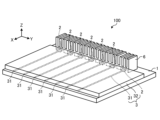
- FIG. 1 is a schematic perspective view showing the configuration of an optical element according to a first embodiment.
- FIG. 2 is an enlarged cross-sectional view taken along line II-II shown in FIG.
- FIG. 3 is an enlarged cross-sectional view taken along line III-III shown in FIG.
- FIG. 4 is an enlarged cross-sectional view taken along line IV-IV shown in FIG.
- FIG. 5 is a schematic cross-sectional view showing the configuration of the optical element according to the second embodiment.
- FIG. 6 is a schematic cross-sectional view showing the configuration of an optical element according to the third embodiment.
- FIG. 7 is a schematic cross-sectional view showing the configuration of an optical element according to the fourth embodiment.
- FIG. 8 is an enlarged cross-sectional view taken along line VIII-VIII shown in FIG.
- FIG. 9 is a schematic perspective view showing the configuration of an optical element according to the fifth embodiment.
- FIG. 10 is a schematic cross-sectional view showing the configuration of the optical element according to the sixth embodiment.
- drawings referred to below may show an orthogonal coordinate system in which the X-axis, Y-axis, and Z-axis directions are defined as being perpendicular to each other, and the positive direction of the Z-axis is the vertically upward direction. Also, the direction of rotation about the vertical axis may be referred to as the ⁇ direction.
- Patent Document 1 discloses an optical element in which a heat sink is directly contacted with the upper surface of a semiconductor laser for the purpose of dissipating heat from the semiconductor laser.
- organic substrate a substrate made of organic resin (hereinafter, referred to as an "organic substrate") as a substrate for an optical element.
- the organic substrate has a lower thermal conductivity than a semiconductor substrate such as a Si substrate or a LiNbO3 substrate, and there is a risk that it will be difficult to ensure heat dissipation using the technology described in Patent Document 1.
- the substrate does not have sufficient heat dissipation properties, the heat generated in the laser will be transmitted to the optical waveguide, causing the refractive index of light in the optical waveguide to change with temperature, which may result in changes in transmission characteristics. For this reason, there is a need for technology that can reduce the heat transfer from the laser to the optical waveguide. Note that this issue can also arise when substrates other than organic substrates are used.
- FIG. 1 is a schematic perspective view showing the configuration of the optical element 100 according to the first embodiment.
- Fig. 2 is an enlarged cross-sectional view taken along line II-II shown in Fig. 1.
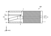
- Fig. 3 is an enlarged cross-sectional view taken along line III-III shown in Fig. 2.
- Fig. 4 is an enlarged cross-sectional view taken along line IV-IV shown in Fig. 3.
- the adhesive 5 is omitted from Fig. 3.
- the optical element 100 shown in Figures 1 to 4 has a substrate 1, a laser 2, an optical waveguide 3, an electrode 4, and a heat sink 6.
- the substrate 1 has, for example, a rectangular plate shape in a plan view.
- the substrate 1 has an upper surface (an example of a first surface) on which the laser 2, the optical waveguide 3, and the electrode 4 are mounted, and a lower surface (an example of a second surface) located opposite the upper surface.
- a solder resist may be located on the upper surface of the substrate 1.
- the substrate 1 may be an organic substrate.
- the substrate 1 may also be a semiconductor substrate.
- the laser 2 is located on the substrate 1. Specifically, the laser 2 is bonded to the upper surface of the substrate 1 using a conductive bonding material 11 such as solder.
- the laser 2 may be, for example, a semiconductor laser.
- the laser 2 has a light-projecting portion (not shown) that projects (irradiates) light toward the optical waveguide 3, which will be described later.
- the optical waveguide 3 is an optical transmission path constructed using a material with optical properties.
- the optical waveguide 3 is located on the substrate 1.
- the optical waveguide 3 has a core 31 that serves as an optical path, and a cladding 32 that surrounds the core 31.
- the core 31 faces the light projecting portion of the laser 2, and extends away from the laser 2 in the positive direction of the X-axis (an example of the first direction).
- the electrode 4 is located on the substrate 1 and connected to the laser 2.
- the electrode 4 includes a first electrode 4a and a second electrode 4b.
- the first electrode 4a is connected to the bottom surface of the laser 2 that faces the substrate 1.
- the second electrode 4b is connected via a wire 7 to the top surface of the laser 2 that is located opposite the bottom surface.
- the electrode 4 is made of metal.
- the electrode 4 has a higher thermal conductivity than the substrate 1.
- the electrode 4 has an elongated shape such that the further it is from the laser 2, the further it is from the optical waveguide 3.
- the electrode 4 has an elongated shape such that it is further away from the laser 2 in the negative direction of the X-axis (an example of the second direction).
- the term "elongated shape" for the electrode 4 does not refer to a state in which the electrode 4 dynamically extends, but rather, for example, refers to the electrode 4 having a band-like shape and the electrode 4 having such a shape being disposed so as to crawl on the substrate 1.
- the electrode 4 which has a higher thermal conductivity than the substrate 1, functions as a heat dissipation path for heat generated in the laser 2.
- the electrode 4 has a shape that extends away from the optical waveguide 3 the farther it is from the laser 2, so that the heat generated in the laser 2 can be dissipated in a direction away from the optical waveguide 3. Therefore, the heat transfer from the laser 2 to the optical waveguide 3 can be reduced.
- the electrodes 4, the first electrode 4a and the second electrode 4b may both be shaped to extend away from the laser 2 in the negative X-axis direction.
- the heat generated in the laser 2 can be dissipated in a direction away from the optical waveguide 3 in both the first electrode 4a and the second electrode 4b. Therefore, the heat transfer from the laser 2 to the optical waveguide 3 can be further reduced.
- the heat sink 6 has a main body 61 and a base 62 that supports the main body 61.
- the main body 61 is located above the laser 2 and the electrode 4.
- One end of the base 62 is located on the substrate 1, and the other end supports the main body 61.
- the one end is the lower end of the base 62, and the other end is the upper end of the base 62.
- the main body 61 is supported by the base 62 at a position higher than the wire 7. In other words, the main body 61 is positioned higher than the wire 7. This configuration makes it possible to reduce interference between the wire 7 and the heat sink 6.
- the optical element 100 may have an adhesive 5 that fixes the heat sink 6 to the substrate 1. As shown in FIG. 4, at least a portion of the adhesive 5 is located in the space surrounded by the body 61, the base 62, and the substrate 1 of the heat sink 6, and covers the laser 2, the first electrode 4a, the second electrode 4b, and the wire 7.
- the adhesive 5 may be, for example, a resin. Hereinafter, it may be referred to as resin 5.
- the adhesive 5 may contain a filler.
- the filler may be contained in greater amounts on the lower side (substrate 1 side) of the adhesive 5 than on the upper side (heat sink 6 side).
- the upper side of the adhesive 5 is the area that contacts the lower surface of the main body 61 of the heat sink 6.
- the heat sink 6 is not located above the optical waveguide 3. In other words, in a plan view, the heat sink 6 does not overlap with the optical waveguide 3. Specifically, when the optical element 100 is viewed in a plan view, the heat sink 6 is located adjacent to the optical waveguide 3. When the optical element 100 is viewed in a plan view, if the heat sink 6 is located along the extension direction of the optical waveguide 3, the side of the heat sink 6 and the end face of the optical waveguide 3 may be disposed at a predetermined distance.
- the thermal effect from the heat sink 6 to the optical waveguide 3 can be reduced compared to a configuration in which the heat sink 6 overlaps with the optical waveguide 3.
- the laser 2, adhesive 5, and heat sink 6 may be arranged in a stepped manner. Specifically, the end of the adhesive 5 on the positive side of the X-axis may be shifted in the negative direction of the X-axis from the end of the laser 2 on the positive side of the X-axis, and the end of the heat sink 6 on the positive side of the X-axis may be shifted in the negative direction of the X-axis from the end of the adhesive 5 on the positive side of the X-axis.
- the thermal effect on the optical waveguide 3 can be further reduced. That is, the heat generated in the laser 2 is transferred to the heat sink 6 via the adhesive 5. Therefore, the temperature of not only the laser 2 but also the adhesive 5 and the heat sink 6 rise.
- the heat sink 6 is farther away from the optical waveguide 3 than when the end of the heat sink 6 on the positive side of the X-axis is aligned with the end of the adhesive 5 on the positive side of the X-axis, so that the effect of the heat generated by the heat sink 6 on the optical waveguide 3 can be made less likely to occur. It is also possible to prevent the adhesive 5 from dripping between the laser 2 and the optical waveguide 3.
- Second Embodiment Fig. 5 is a schematic cross-sectional view showing the configuration of an optical element 100 according to the second embodiment.
- the adhesive 5 is omitted in Fig. 5.
- the electrode 4 may have a width in a portion farther from the laser 2 than in a portion closer to the laser 2.
- the first electrode 4a and the second electrode 4b each have a first portion 41 closer to the laser 2 and a second portion 42 farther from the laser 2 than the first portion 41.
- the width W1 of the second portion 42 may be wider than the width W2 of the first portion 41.
- the width W3 of the second portion 42 may be wider than the width W4 of the first portion 41.
- the widths (W1, W2, W3, and W4) refer to the length in the direction (Y-axis direction) along the top surface (first surface) of the substrate 1, as shown in FIG. 5.
- the surface area of the electrode 4 is increased, and the heat dissipation effect of the electrode 4 can be further improved.
- the electrode 4 may have a tapered shape that becomes wider as it moves away from the laser 2.
- FIG. 6 is a schematic cross-sectional view showing the configuration of an optical element 100 according to the third embodiment.
- the body 61 of the heat sink 6 may have a portion located below the upper surface of the laser 2. Specifically, the body 61 has a first portion 611 located above the laser 2 and a second portion 612 located above the first electrode 4a. In this case, the lower surface of the second portion 612 may be located below the upper surface of the laser 2.
- This configuration allows the heat sink 6 to be closer to the electrode 4. This makes it harder for heat to escape from the heat transfer path from the laser 2 and electrode 4 to the heat sink 6, further improving heat dissipation.
- Fig. 7 is a schematic cross-sectional view showing the configuration of an optical element 100 according to a fourth embodiment.
- Fig. 8 is an enlarged cross-sectional view taken along line VIII-VIII shown in Fig. 7.
- the adhesive 5 is omitted in Fig. 7.
- the substrate 1 may have a solder resist 12.
- the solder resist 12 is located on a portion of the upper surface of the substrate 1.
- the electrode 4 has copper foil 43 located on the upper surface of the substrate 1 and gold 44 located on the copper foil 43.
- the solder resist 12 is located in the mounting area of the laser 2. Specifically, in a plan view, the solder resist 12 is located in an area slightly larger than the area where the substrate 1 and the laser 2 overlap. In this case, as shown in FIG. 8, at least a portion of the side of the copper foil 43 located outside the mounting area of the laser 2 may be exposed from the solder resist 12.
- the optical element 100 may have a plurality of lasers 2, a plurality of cores 31, and a plurality of electrodes 4 (not shown).
- the plurality of lasers 2 are arranged in a direction perpendicular to the first direction (an example of the third direction, here the Y-axis direction).
- the plurality of cores 31 and the plurality of electrodes 4 are also arranged in a direction perpendicular to the first direction (an example of the third direction, here the Y-axis direction).
- FIG. 10 is a schematic cross-sectional view showing the configuration of an optical element 100 according to a sixth embodiment.
- the adhesive 5 is omitted in Fig. 10.
- the shape of the electrode 4 is not limited to the shape shown in Fig. 3.
- the electrode 4 may have a shape that extends obliquely away from the laser 2.
- the first electrode 4a may extend obliquely with respect to the negative X-axis direction.
- the electrode 4 has a shape that extends away from the optical waveguide 3 the farther it is from the laser 2, so heat generated in the laser 2 can be dissipated in a direction away from the optical waveguide 3. This reduces heat transfer from the laser 2 to the optical waveguide 3.
- the second electrode 4b may also extend obliquely away from the laser 2, similar to the first electrode 4a.
- an optical element for example, optical element 100
- a substrate for example, substrate 1
- a laser for example, laser 2
- an optical waveguide for example, optical waveguide 3
- electrodes for example, first electrode 4a and second electrode 4b
- the laser is located on the substrate.
- the optical waveguide is located on the substrate and has a core (for example, core 31) at a position facing the light-emitting portion of the laser.
- the electrodes are located on the substrate and connected to the laser. The electrodes are shaped to extend further away from the optical waveguide the further away they are from the laser.
- the core may be shaped to extend away from the laser in a first direction
- the electrodes may be shaped to extend away from the laser in a second direction that is opposite to the first direction
- the electrodes may be covered with a resin (for example, adhesive 5).
- the electrodes include a first electrode (for example, first electrode 4a) connected to a first surface of the laser facing the substrate, and a second electrode (for example, second electrode 4b) connected via a wire (for example, wire 7) to a second surface of the laser located opposite the first surface, and both the first electrode and the second electrode may be shaped to extend away from the laser in the second direction.
- the optical element of (4) above has a heat sink (for example, heat sink 6) having a body portion (for example, body portion 61) located above the laser and electrode, and a base portion (base portion 62) located to the side of the laser and electrode, one end of which is located on the substrate, and the other end of which supports the body portion, and the body portion may be located above the wire.
- a heat sink for example, heat sink 6
- body portion for example, body portion 61
- base portion 62 located to the side of the laser and electrode, one end of which is located on the substrate, and the other end of which supports the body portion, and the body portion may be located above the wire.
- the optical element of (5) above has an adhesive (for example, adhesive 5) that fixes the heat sink to the substrate, and at least a portion of the adhesive is located in the space surrounded by the main body, the base, and the substrate, and may cover the laser, the first electrode, the second electrode, and the wire.
- adhesive for example, adhesive 5
- the body of the heat sink has a first portion (for example, first portion 611) located above the laser and a second portion (for example, second portion 612) located above the electrode, and the bottom surface of the second portion may be located below the top surface of the laser.
- the heat sink may not overlap the optical waveguide in a plan view.
- the end of the adhesive on the first direction side may be offset in the second direction from the end of the laser on the first direction side, and the end of the heat sink on the first direction side may be offset in the second direction from the end of the adhesive on the first direction side.
- the electrode has a first portion (for example, first portion 41) close to the laser and a second portion (for example, second portion 42) farther from the laser than the first portion, and the width of the second portion may be wider than the width of the first portion.
- the substrate has a first surface on which the laser, optical waveguide, and electrodes are mounted, a second surface opposite the first surface, and solder resist (for example, solder resist 12) located on a portion of the first surface, the electrodes have copper foil (for example, copper foil 43) located on the first surface, the solder resist is located in the mounting area of the laser, and at least a portion of the side of the copper foil located outside the mounting area may be exposed from the solder resist.
- solder resist for example, solder resist 12
Landscapes
- Physics & Mathematics (AREA)
- Condensed Matter Physics & Semiconductors (AREA)
- General Physics & Mathematics (AREA)
- Electromagnetism (AREA)
- Optics & Photonics (AREA)
- Semiconductor Lasers (AREA)
Priority Applications (1)
| Application Number | Priority Date | Filing Date | Title |
|---|---|---|---|
| JP2025504015A JPWO2024181571A1 (https=) | 2023-03-02 | 2024-03-01 |
Applications Claiming Priority (2)
| Application Number | Priority Date | Filing Date | Title |
|---|---|---|---|
| JP2023032073 | 2023-03-02 | ||
| JP2023-032073 | 2023-03-02 |
Publications (1)
| Publication Number | Publication Date |
|---|---|
| WO2024181571A1 true WO2024181571A1 (ja) | 2024-09-06 |
Family
ID=92590677
Family Applications (1)
| Application Number | Title | Priority Date | Filing Date |
|---|---|---|---|
| PCT/JP2024/007883 Ceased WO2024181571A1 (ja) | 2023-03-02 | 2024-03-01 | 光学素子 |
Country Status (2)
| Country | Link |
|---|---|
| JP (1) | JPWO2024181571A1 (https=) |
| WO (1) | WO2024181571A1 (https=) |
Citations (7)
| Publication number | Priority date | Publication date | Assignee | Title |
|---|---|---|---|---|
| JPH0961676A (ja) * | 1995-08-30 | 1997-03-07 | Hitachi Ltd | 光アセンブリ |
| JPH11211924A (ja) * | 1998-01-21 | 1999-08-06 | Nippon Telegr & Teleph Corp <Ntt> | 波長多重通信用光回路 |
| JP2004006749A (ja) * | 2002-03-29 | 2004-01-08 | Matsushita Electric Ind Co Ltd | 光デバイス、その製造方法、光モジュール、光伝送システム |
| JP2006053472A (ja) * | 2004-08-16 | 2006-02-23 | Sony Corp | 光導波モジュール及び光情報処理装置 |
| JP2007328201A (ja) * | 2006-06-08 | 2007-12-20 | Nippon Telegr & Teleph Corp <Ntt> | 光集積回路 |
| CN212304182U (zh) * | 2020-04-15 | 2021-01-05 | 天津市光纳电子科技有限公司 | 一种低噪高散热的激光器保护壳 |
| WO2022176992A1 (ja) * | 2021-02-19 | 2022-08-25 | 京セラ株式会社 | 発光装置 |
-
2024
- 2024-03-01 JP JP2025504015A patent/JPWO2024181571A1/ja active Pending
- 2024-03-01 WO PCT/JP2024/007883 patent/WO2024181571A1/ja not_active Ceased
Patent Citations (7)
| Publication number | Priority date | Publication date | Assignee | Title |
|---|---|---|---|---|
| JPH0961676A (ja) * | 1995-08-30 | 1997-03-07 | Hitachi Ltd | 光アセンブリ |
| JPH11211924A (ja) * | 1998-01-21 | 1999-08-06 | Nippon Telegr & Teleph Corp <Ntt> | 波長多重通信用光回路 |
| JP2004006749A (ja) * | 2002-03-29 | 2004-01-08 | Matsushita Electric Ind Co Ltd | 光デバイス、その製造方法、光モジュール、光伝送システム |
| JP2006053472A (ja) * | 2004-08-16 | 2006-02-23 | Sony Corp | 光導波モジュール及び光情報処理装置 |
| JP2007328201A (ja) * | 2006-06-08 | 2007-12-20 | Nippon Telegr & Teleph Corp <Ntt> | 光集積回路 |
| CN212304182U (zh) * | 2020-04-15 | 2021-01-05 | 天津市光纳电子科技有限公司 | 一种低噪高散热的激光器保护壳 |
| WO2022176992A1 (ja) * | 2021-02-19 | 2022-08-25 | 京セラ株式会社 | 発光装置 |
Also Published As
| Publication number | Publication date |
|---|---|
| JPWO2024181571A1 (https=) | 2024-09-06 |
Similar Documents
| Publication | Publication Date | Title |
|---|---|---|
| US7198412B2 (en) | Holder of optical transmission lines and multi-core optical wave-guide | |
| CN103370644B (zh) | 光学电路板 | |
| JP2009105173A (ja) | 光源モジュール | |
| JP7032942B2 (ja) | 光導波路および光回路基板 | |
| JP7337167B2 (ja) | 光回路基板およびそれを用いた電子部品実装構造体 | |
| CN106373975A (zh) | 半导体器件 | |
| US8168940B2 (en) | Optical transmission module, electronic device and method for manufacturing optical transmission module | |
| TWI693437B (zh) | 光波導及光電路基板 | |
| JP4306011B2 (ja) | 光配線層及びその製造方法並びに光・電気配線基板及びその製造方法並びに実装基板 | |
| CN114077016B (zh) | 具有光子集成电路的封装结构 | |
| WO2024181571A1 (ja) | 光学素子 | |
| JP5349192B2 (ja) | 光配線構造およびそれを具備する光モジュール | |
| CN113009647B (zh) | 一种光模块 | |
| JP4674692B2 (ja) | 面状照明装置 | |
| JP7645857B2 (ja) | 半導体光デバイスおよび半導体光デバイスの製造方法 | |
| JP6204177B2 (ja) | 光装置用基板およびそれを備えた光装置 | |
| JP2007178950A (ja) | 光配線基板および光配線モジュール | |
| TWI915128B (zh) | 具光子晶片的封裝結構及其製造方法 | |
| CN113711097B (zh) | 波导部件和波导层叠体 | |
| WO2018180785A1 (ja) | 光電気配線基板 | |
| TWI802812B (zh) | 具有光子集成電路的封裝結構 | |
| JP7027091B2 (ja) | 光導波路および光回路基板 | |
| WO2024204657A1 (ja) | 光導波路パッケージ及び光源モジュール | |
| JP2024131646A (ja) | 光モジュール | |
| WO2025234295A1 (ja) | 光学部品および光モジュール |
Legal Events
| Date | Code | Title | Description |
|---|---|---|---|
| 121 | Ep: the epo has been informed by wipo that ep was designated in this application |
Ref document number: 24764048 Country of ref document: EP Kind code of ref document: A1 |
|
| ENP | Entry into the national phase |
Ref document number: 2025504015 Country of ref document: JP Kind code of ref document: A |
|
| WWE | Wipo information: entry into national phase |
Ref document number: 2025504015 Country of ref document: JP |
|
| NENP | Non-entry into the national phase |
Ref country code: DE |
|
| 122 | Ep: pct application non-entry in european phase |
Ref document number: 24764048 Country of ref document: EP Kind code of ref document: A1 |