WO2024180611A1 - ウエハ載置台 - Google Patents
ウエハ載置台 Download PDFInfo
- Publication number
- WO2024180611A1 WO2024180611A1 PCT/JP2023/007066 JP2023007066W WO2024180611A1 WO 2024180611 A1 WO2024180611 A1 WO 2024180611A1 JP 2023007066 W JP2023007066 W JP 2023007066W WO 2024180611 A1 WO2024180611 A1 WO 2024180611A1
- Authority
- WO
- WIPO (PCT)
- Prior art keywords
- plug
- hole
- wafer mounting
- outer edge
- mounting table
- Prior art date
- Legal status (The legal status is an assumption and is not a legal conclusion. Google has not performed a legal analysis and makes no representation as to the accuracy of the status listed.)
- Ceased
Links
Images






Classifications
-
- H—ELECTRICITY
- H01—ELECTRIC ELEMENTS
- H01J—ELECTRIC DISCHARGE TUBES OR DISCHARGE LAMPS
- H01J37/00—Discharge tubes with provision for introducing objects or material to be exposed to the discharge, e.g. for the purpose of examination or processing thereof
- H01J37/32—Gas-filled discharge tubes
- H01J37/32431—Constructional details of the reactor
- H01J37/32715—Workpiece holder
-
- B—PERFORMING OPERATIONS; TRANSPORTING
- B23—MACHINE TOOLS; METAL-WORKING NOT OTHERWISE PROVIDED FOR
- B23K—SOLDERING OR UNSOLDERING; WELDING; CLADDING OR PLATING BY SOLDERING OR WELDING; CUTTING BY APPLYING HEAT LOCALLY, e.g. FLAME CUTTING; WORKING BY LASER BEAM
- B23K26/00—Working by laser beam, e.g. welding, cutting or boring
- B23K26/20—Bonding
- B23K26/21—Bonding by welding
-
- H—ELECTRICITY
- H10—SEMICONDUCTOR DEVICES; ELECTRIC SOLID-STATE DEVICES NOT OTHERWISE PROVIDED FOR
- H10P—GENERIC PROCESSES OR APPARATUS FOR THE MANUFACTURE OR TREATMENT OF DEVICES COVERED BY CLASS H10
- H10P72/00—Handling or holding of wafers, substrates or devices during manufacture or treatment thereof
- H10P72/04—Apparatus for manufacture or treatment
- H10P72/0431—Apparatus for thermal treatment
- H10P72/0434—Apparatus for thermal treatment mainly by convection
-
- H—ELECTRICITY
- H10—SEMICONDUCTOR DEVICES; ELECTRIC SOLID-STATE DEVICES NOT OTHERWISE PROVIDED FOR
- H10P—GENERIC PROCESSES OR APPARATUS FOR THE MANUFACTURE OR TREATMENT OF DEVICES COVERED BY CLASS H10
- H10P72/00—Handling or holding of wafers, substrates or devices during manufacture or treatment thereof
- H10P72/70—Handling or holding of wafers, substrates or devices during manufacture or treatment thereof for supporting or gripping
- H10P72/72—Handling or holding of wafers, substrates or devices during manufacture or treatment thereof for supporting or gripping using electrostatic chucks
-
- H—ELECTRICITY
- H10—SEMICONDUCTOR DEVICES; ELECTRIC SOLID-STATE DEVICES NOT OTHERWISE PROVIDED FOR
- H10P—GENERIC PROCESSES OR APPARATUS FOR THE MANUFACTURE OR TREATMENT OF DEVICES COVERED BY CLASS H10
- H10P72/00—Handling or holding of wafers, substrates or devices during manufacture or treatment thereof
- H10P72/70—Handling or holding of wafers, substrates or devices during manufacture or treatment thereof for supporting or gripping
- H10P72/72—Handling or holding of wafers, substrates or devices during manufacture or treatment thereof for supporting or gripping using electrostatic chucks
- H10P72/722—Details of electrostatic chucks
-
- H—ELECTRICITY
- H01—ELECTRIC ELEMENTS
- H01J—ELECTRIC DISCHARGE TUBES OR DISCHARGE LAMPS
- H01J2237/00—Discharge tubes exposing object to beam, e.g. for analysis treatment, etching, imaging
- H01J2237/20—Positioning, supporting, modifying or maintaining the physical state of objects being observed or treated
- H01J2237/2007—Holding mechanisms
Definitions
- the present invention relates to a wafer mounting table.
- the wafer mounting table of Patent Document 1 includes a ceramic plate having a wafer mounting surface and a built-in heater, a ventilation path provided in the ceramic plate, and a breathable member arranged in the ventilation path.
- the breathable member include a member made of a porous body and a member provided with one or more through holes.
- Methods of fixing the breathable member to the ventilation path include a method of pressing the breathable member into the ventilation path and a method of adhering the breathable member to the ventilation path using an adhesive. It is also described that it is preferable to form a protrusion or the like on the inner wall of the ventilation path to lock the breathable member so that the breathable member does not move due to vacuum suction.
- the present invention was made to solve the above-mentioned problems, and its main objective is to provide a simple structure that allows the plug to be removed from the plug placement hole.
- the wafer mounting table of the present invention comprises: a ceramic plate having a wafer mounting surface on an upper surface thereof and incorporating an electrode; a plug placement hole extending from the lower surface to the upper surface of the ceramic plate; a plug disposed in the plug placement hole and allowing gas to pass therethrough; a plug joint portion that joins an upper surface outer edge of the plug and an upper opening edge of the plug placement hole and is provided so as to cover the upper surface outer edge of the plug from above; It is equipped with the following:
- a plug through which gas can pass is placed in the plug placement hole.
- the outer edge of the top surface of the plug and the upper opening edge of the plug placement hole are joined by a plug joint.
- the plug joint is provided so as to cover the outer edge of the top surface of the plug from above.
- the plug joint is provided so as to hook onto the upper outer edge of the plug, thereby preventing the plug from slipping upward out of the plug placement hole. In this way, with a simple structure in which the outer edge of the top surface of the plug is covered from above by the plug joint, it is possible to prevent the plug from slipping upward out of the plug placement hole.
- the plug bonding portion may be provided around the entire outer edge of the upper surface of the plug. In this way, the plug bonding portion is provided around the entire circumference of the plug, thereby increasing the bonding strength of the plug bonding portion.
- the plug joint may be partially present at two or more locations along the circumferential direction of the outer edge of the upper surface of the plug. In this way, since the plug joint is provided so as to be partially present at two or more locations along the circumferential direction, rather than along the entire circumference of the outer edge of the upper surface of the plug, it is easy to remove the plug joint later. For example, if the need arises to replace the plug, the plug replacement work will be facilitated.
- the plug may have an inclined plug surface on the outer edge of the upper surface
- the plug mounting hole may have an inclined hole surface on the upper opening edge
- the plug joint may be a sprayed portion provided so as to fill the groove formed by the plug inclined surface and the inclined hole surface.
- the inclined surface may be flat or curved (concave or convex).
- the plug joint may be a laser welded portion formed by laser welding the outer edge of the upper surface of the plug and the upper opening edge of the plug placement hole.
- the plug joint can be formed relatively easily by laser welding.
- the plug joint which is a laser welded portion
- the plug joint is provided so as to be partially present in two or more places along the circumferential direction, the number of welded places is reduced, thereby reducing the risk of cracks occurring due to laser welding.
- the work of removing the old plug is made easier because there are fewer laser welds to be removed.
- the laser weld may have an inverted triangular shape when viewed in vertical cross section, with the bottom of the laser weld located on the plug side. In this way, the laser irradiation position in the process of forming the laser weld is on the plug side. Therefore, even if laser irradiation is performed, cracks are unlikely to occur in the ceramic plate. If a crack occurs in the ceramic plate, the crack may cause communication between the plug placement hole and the electrode, but this can be prevented.
- the wafer mounting table of the present invention may further include a conductive plate bonded to the lower surface of the ceramic plate and provided with a gas supply passage communicating with the plug placement hole.
- the conductive plate may be used as a cooling plate for cooling the ceramic plate, or as a high-frequency electrode for generating plasma above the wafer mounting surface.
- FIG. FIG. FIG. 2 is a partially enlarged view of FIG. 5A to 5C are diagrams showing the manufacturing process of the wafer mounting table 10.
- FIG. 2 is an enlarged vertical cross-sectional view of a wafer mounting table 110 having a plug bonding portion 160.
- FIG. 5A to 5C are diagrams showing a manufacturing process of the wafer mounting table 110.
- FIG. 2 is a vertical cross-sectional view of the wafer mounting table 210.
- FIG. 2 is an enlarged vertical cross-sectional view of a wafer mounting table having a plug bonding portion 260.
- FIG. 13 is an enlarged vertical cross-sectional view of a wafer mounting table having a plug bonding portion 360.
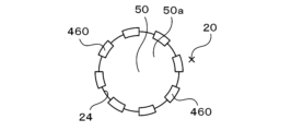
- FIG. 4 is a plan view of the periphery of the plug joint 460.
- FIG. 4 is a plan view of the periphery of the plug joint 466.
- FIG. 13 is an enlarged vertical cross-sectional view of a wafer mounting table having a plug bonding portion
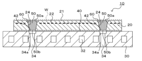
- Fig. 1 is a vertical cross-sectional view of a wafer mounting table 10
- Fig. 2 is a plan view of a ceramic plate 20
- Fig. 3 is an enlarged view of a portion of Fig. 1.
- the wafer mounting table 10 includes a ceramic plate 20, a plug placement hole 24, a base plate (conductive plate) 30, a metal bonding layer 40, a plug 50, and a plug bonding portion 60.
- the ceramic plate 20 is a ceramic circular plate (e.g., 300 mm in diameter, 5 mm in thickness) made of alumina sintered body or aluminum nitride sintered body.
- the upper surface of the ceramic plate 20 is the wafer mounting surface 21.
- the ceramic plate 20 has an electrode 22 built in.
- the wafer mounting surface 21 of the ceramic plate 20 has a seal band 21a formed along the outer edge, and a plurality of circular small protrusions 21b formed on the entire surface.
- the seal band 21a and the circular small protrusions 21b have the same height, for example, several ⁇ m to several tens of ⁇ m.
- the electrode 22 is a flat mesh electrode used as an electrostatic electrode, and a DC voltage can be applied to it.
- the wafer W When a DC voltage is applied to the electrode 22, the wafer W is attracted and fixed to the wafer mounting surface 21 (specifically, the upper surface of the seal band 21a and the upper surface of the circular small protrusions 21b) by electrostatic attraction force, and when the application of the DC voltage is released, the wafer W is released from the wafer mounting surface 21.
- the portion of the wafer mounting surface 21 on which the seal band 21a and small circular protrusions 21b are not provided is referred to as the reference surface 21c.
- the plug arrangement hole 24 is a hole that extends from the lower surface to the upper surface of the ceramic plate 20, and in this case is a through hole that penetrates the ceramic plate 20 in the vertical direction.
- the plug arrangement hole 24 faces the gas hole 34 of the base plate 30.
- the plug arrangement hole 24 penetrates the electrode 22 in the vertical direction, but the electrode 22 is not exposed on the inner surface of the plug arrangement hole 24.
- the plug arrangement hole 24 is a tapered hole having a truncated cone space in which the area of the upper opening is larger than the area of the lower opening.
- the upper opening edge of the plug arrangement hole 24 is chamfered all around to form an arrangement hole inclined surface 24c.
- the arrangement hole inclined surface 24c is a flat surface rather than a curved surface.
- the plug arrangement hole 24 is provided in multiple locations on the ceramic plate 20 (for example, multiple locations that are equally spaced along the circumferential direction).
- the base plate 30 is a conductive disk (a disk with the same diameter as or larger than the ceramic plate 20) with good thermal conductivity.
- a refrigerant e.g., an electrically insulating liquid such as a fluorine-based inert liquid
- the gas hole 34 is provided to penetrate the base plate 30 in the vertical direction and has a large diameter portion 34a at the top.
- the large diameter portion 34a includes the lower opening of the plug arrangement hole 24 in a plan view.
- the refrigerant flow path 32 is formed in a single stroke from the inlet to the outlet over the entire surface of the base plate 30 in a plan view.
- Examples of materials for the base plate 30 include metals and composite materials. Examples of metals include Mo. Examples of composite materials include composite materials of metal and ceramic. Examples of composite materials of metal and ceramic include metal matrix composite materials (metal matrix composites (MMC)) and ceramic matrix composite materials (ceramic matrix composites (CMC)). Specific examples of such composite materials include materials containing Si, SiC, and Ti, and materials in which a porous SiC body is impregnated with Al and/or Si. A material containing Si, SiC, and Ti is called SiSiCTi, a material in which a porous SiC body is impregnated with Al is called AlSiC, and a material in which a porous SiC body is impregnated with Si is called SiSiC.
- the base plate 30 is also used as an RF electrode. Specifically, an upper electrode (not shown) is disposed above the wafer mounting surface 21, and when high-frequency power is applied between the parallel plate electrodes consisting of the upper electrode and the base plate 30, plasma is generated.
- the metal bonding layer 40 bonds the lower surface of the ceramic plate 20 and the upper surface of the base plate 30.
- the metal bonding layer 40 is formed, for example, by TCB (thermal compression bonding).
- TCB refers to a known method in which a metal bonding material is sandwiched between two members to be bonded, and the two members are pressure-bonded while being heated to a temperature below the solidus temperature of the metal bonding material.
- the metal bonding layer 40 may be a layer formed of solder or metal brazing material.
- the metal bonding layer 40 has a through hole 42. The through hole 42 is provided at a position facing the large diameter portion 34a of the gas hole 34.
- the through hole 42 is provided coaxially with the large diameter portion 34a, and the diameter of the through hole 42 is the same as the diameter of the large diameter portion 34a.
- “matching” includes not only a case of perfect matching, but also a case of substantial matching (for example, a case within the tolerance range) (the same applies below).
- the plug 50 is placed in the plug placement hole 24.
- the plug 50 is an electrically insulating member that allows gas to flow in the vertical direction.
- the plug 50 is a ceramic porous body, and for example, a porous body of the same material as the ceramic plate 20 can be used.
- the porosity of the plug 50 is preferably 30% or more, and the average pore diameter is preferably 20 ⁇ m or more.
- the upper outer edge of the plug 50 is chamfered all around to form a plug inclined surface 50c.
- the plug inclined surface 50c is flat, not curved.
- the plug 50 is a truncated cone-shaped member whose upper surface area is larger than the lower surface area. Therefore, the plug 50 does not slip out downward from the plug placement hole 24.
- the upper surface 50a of the plug 50 is exposed to the upper opening of the plug placement hole 24 and is flush with the reference surface 21c.
- “same” includes not only completely identical, but also substantially identical (for example, within the range of tolerance) (the same applies below).
- the plug 50 and the plug placement hole 24 are designed in advance so that when the plug 50 is inserted into the plug placement hole 24 and the outer peripheral surface of the plug 50 is aligned with the inner peripheral surface of the plug placement hole 24, the height of the upper surface 50a of the plug 50 is aligned with the height of the reference surface 21c of the ceramic plate 20. Therefore, the upper surface 50a of the plug 50 and the reference surface 21c of the ceramic plate 20 can be easily aligned on the same plane.
- the height of the lower surface 50b of the plug 50 may be the same as the height of the lower surface of the ceramic plate 20, or it may be higher or lower.
- the plug joint 60 joins the outer edge of the upper surface of the plug 50 to the upper opening edge of the plug arrangement hole 24, and is provided so as to cover the outer edge of the upper surface of the plug 50 and the upper opening edge of the plug arrangement hole 24 from above.
- the plug joint 60 is formed by filling a groove formed by the plug inclined surface 50c provided around the entire circumference of the outer edge of the upper surface of the plug 50 and the arrangement hole inclined surface 24c provided around the entire circumference of the upper opening edge of the plug arrangement hole 24 with a ceramic material by a thermal spraying method.
- the inclined surfaces 24c, 50c are flat surfaces rather than curved surfaces.
- This groove is ring-shaped in a plan view and has a V-shaped cross section.
- Both the plug inclined surface 50c and the arrangement hole inclined surface 24c are covered from above by the plug joint 60.
- the upper surface of the plug joint 60 is flush with the upper surface 50a of the plug 50 and the reference surface 21c of the wafer mounting surface 21.
- the height of the upper surface of the plug joint 60 may protrude from the reference surface 21c within a range that does not exceed the height of the upper surface of the small circular protrusion 21b, or may be slightly recessed from the reference surface 21c.
- the wafer W is placed on the wafer mounting surface 21 with the wafer mounting table 10 installed in a chamber (not shown).
- the chamber is then depressurized by a vacuum pump to adjust the pressure inside the chamber to a predetermined degree of vacuum, and a direct current voltage is applied to the electrode 22 of the ceramic plate 20 to generate an electrostatic adsorption force, and the wafer W is adsorbed and fixed to the wafer mounting surface 21 (specifically, the upper surface of the seal band 21a or the upper surface of the circular small protrusion 21b).
- a reaction gas atmosphere of a predetermined pressure (for example, several tens to several hundreds of Pa) is created inside the chamber, and in this state, a high-frequency voltage is applied between an upper electrode (not shown) provided on the ceiling part of the chamber and the base plate 30 of the wafer mounting table 10 to generate plasma.
- the surface of the wafer W is treated by the generated plasma.
- a coolant is circulated through the coolant flow path 32 of the base plate 30.
- a backside gas is introduced into the gas hole 34 from a gas cylinder (not shown).
- a thermally conductive gas (for example, helium) is used as the backside gas.
- the backside gas is supplied and sealed in the space between the back surface of the wafer W and the reference surface 21c of the wafer mounting surface 21 through the gas hole 34, the through hole 42, and the plug 50.
- This backside gas ensures efficient thermal conduction between the wafer W and the ceramic plate 20.
- FIG. 4 is a manufacturing process diagram of the wafer mounting table 10.
- the ceramic plate 20 incorporates an electrode 22 and has a plug arrangement hole 24.
- the upper opening edge of the plug arrangement hole 24 is chamfered to form an arrangement hole inclined surface 24c.
- the base plate 30 has a refrigerant flow path 32 and a gas hole 34.
- the gas hole 34 has a large diameter portion 34a at the top.
- the metal bonding material 90 has a through hole 92 at a position opposite the large diameter portion 34a of the gas hole 34.
- a metal bonding material 90 is sandwiched between the lower surface of the ceramic plate 20 and the upper surface of the base plate 30 to form a laminate.
- the plug placement hole 24 of the ceramic plate 20, the through hole 92 of the metal bonding material 90, and the gas hole 34 of the base plate 30 are stacked so that they are coaxial.
- the laminate is pressed and bonded at a temperature below the solidus temperature of the metal bonding material 90 (for example, a temperature equal to or higher than the solidus temperature minus 20°C and lower than the solidus temperature), and then returned to room temperature (TCB).
- the metal bonding material 90 and the through hole 92 become the metal bonding layer 40 and the through hole 42, respectively, and a bonded body 94 in which the ceramic plate 20 and the base plate 30 are bonded by the metal bonding layer 40 is obtained ( Figure 4B).
- an Al-Mg-based bonding material or an Al-Si-Mg-based bonding material can be used as the metal bonding material 90. It is preferable to use a metal bonding material 90 with a thickness of about 100 ⁇ m.
- a plug 50 having a truncated cone shape is prepared (Fig. 4B).
- the outer edge of the upper surface of the plug 50 is chamfered to form a plug inclined surface 50c.
- the plug 50 is inserted into the plug arrangement hole 24 (Fig. 4C).
- the plug inclined surface 50c of the plug 50 and the arrangement hole inclined surface 24c of the plug arrangement hole 24 form a groove 70 that is ring-shaped in plan view and has a V-shaped cross section.
- the groove 70 is filled with a ceramic material by thermal spraying.
- the groove 70 is filled with the plug joint 60.
- the plug inclined surface 50c and the arrangement hole inclined surface 24c are covered from above by the plug joint 60.
- the raised portion of the plug joint 60 is made flat by grinding.
- the wafer mounting table 10 is obtained by providing a seal band 21a and small circular protrusions 21b on the upper surface of the ceramic plate 20 ( Figure 4D).
- the plug joint 60 may be formed by thermal spraying after providing the seal band 21a and small circular protrusions 21b on the upper surface of the ceramic plate 20.
- a plug 50 through which gas can pass is placed in the plug placement hole 24.
- the upper outer edge of the plug 50 and the upper opening edge of the plug placement hole 24 are joined by a plug joint 60.
- the plug joint 60 is provided so as to cover the upper outer edge of the plug 50 from above, thereby preventing the plug 50 from slipping out upward from the plug placement hole 24. In this way, with a simple structure in which the upper outer edge of the plug 50 is covered from above with the plug joint 60, it is possible to prevent the plug 50 from slipping out upward from the plug placement hole 24.
- the plug joint 60 is provided around the entire circumference of the plug 50, the joint strength of the plug joint 60 is increased.
- the plug joint 60 is a sprayed portion that is provided to fill the groove 70 formed by the plug inclined surface 50c and the placement hole inclined surface 24c. Therefore, the plug joint 60 can be formed relatively easily by spraying.
- Fig. 5 is an enlarged vertical cross-sectional view of the wafer mounting table 110 equipped with a plug bonding portion 160
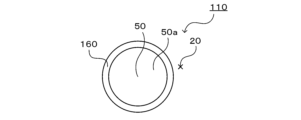
- Fig. 6 is a plan view of the periphery of the plug 160
- Fig. 7 is a manufacturing process diagram (part) of the wafer mounting table 110. Note that in Figs. 5 to 7, the same components of the wafer mounting table 110 as those of the wafer mounting table 10 are denoted by the same reference numerals, and description thereof will be omitted.
- the wafer mounting table 110 includes a ceramic plate 20, a plug placement hole 24, a base plate (conductive plate) 30, a metal bonding layer 40, a plug 50, and a plug bonding portion 160.
- the plug joint 160 is a laser welded portion formed by laser welding the outer edge of the top surface of the plug 50 to the upper opening edge of the plug arrangement hole 24.
- the plug joint 160 has an inverted triangular shape, with the bottom of the plug joint 160 located at the boundary between the plug 50 and the plug arrangement hole 24.
- This plug joint 160 joins the outer edge of the top surface of the plug 50 to the upper opening edge of the plug arrangement hole 24, and is provided so as to cover the outer edge of the top surface of the plug 50 and the upper opening edge of the plug arrangement hole 24 from above.
- the plug joint 160 is provided around the entire circumference of the outer edge of the top surface of the plug 50.
- the use of the wafer mounting table 110 is similar to that of the wafer mounting table 10, so a detailed explanation is omitted.
- a manufacturing example of the wafer mounting table 110 that is different from the manufacturing example of the wafer mounting table 10 will be described.
- the upper opening edge of the plug arrangement hole 24 was chamfered to form the arrangement hole inclined surface 24c
- the upper surface outer edge of the plug 50 was chamfered to form the plug inclined surface 50c.
- such chamfering is not performed. Therefore, when the plug 50 is inserted into the plug arrangement hole 24, the upper opening edge of the plug arrangement hole 24 and the upper surface outer edge of the plug 50 are in contact with each other (FIG. 7A).
- a laser e.g., a nanosecond laser, a picosecond laser, a femtosecond laser, etc.
- a laser is irradiated to the boundary between the upper opening edge of the plug arrangement hole 24 and the upper surface outer edge of the plug 50 to locally heat it up.
- the upper opening edge of the plug arrangement hole 24 and the upper surface outer edge of the plug 50 are welded to form a laser welded portion. Due to the nature of laser welding, the cross section of the laser weld gets smaller in width (diameter) from top to bottom. Any raised parts of the laser weld that rise above the surface are ground flat. This forms the plug joint 160 ( Figure 7B).
- the plug joint 160 is provided so as to cover the outer edge of the upper surface of the plug 50 from above.
- the plug joint 160 is provided so as to hook onto the upper outer edge of the plug 50, thereby preventing the plug 50 from slipping out upward from the plug placement hole 24. In this way, with a simple structure in which the outer edge of the upper surface of the plug 50 is covered from above with the plug joint 160, it is possible to prevent the plug 50 from slipping out upward from the plug placement hole 24.
- the plug joint 160 is provided around the entire outer edge of the upper surface of the plug 50, the joint strength of the plug joint 160 is increased.
- the plug joint 160 is a laser welded portion formed by laser welding the boundary between the outer edge of the top surface of the plug 50 and the upper opening edge of the plug placement hole 24. Therefore, the plug joint 160 can be formed relatively easily by laser welding. When the plug joint 160 is formed by laser welding, there is no need to chamfer the outer edge of the top surface of the plug 50 or the upper opening edge of the plug placement hole 24 as in the first embodiment.
- the plug 50 made of a porous material is exemplified as a plug that allows gas to flow in the vertical direction, but this is not particularly limited.
- a dense plug having a flow path (e.g., a straight flow path or a spiral flow path) inside that allows gas to flow in the vertical direction may be used as such a plug.
- a plug 50 having a truncated cone shape is illustrated, but this is not particularly limited.
- a plug having a cylindrical shape may also be used.
- a stepped hole having a large diameter portion 34a above the gas hole 34 is used, but this is not particularly limited.
- a straight hole may be used as the gas hole 34.
- an electrostatic electrode is exemplified as the electrode 22 built into the ceramic plate 20, but this is not particularly limited.
- a heater electrode resistive heating element
- an RF electrode may be built into the ceramic plate 20.
- the ceramic plate 20 and the base plate 30 are joined by a metal joining layer 40, but a resin adhesive layer may be used instead of the metal joining layer 40.
- the base plate 30 is provided with gas holes 34 that form a gas supply path, but the present invention is not limited to this.
- the base plate 30 may be provided with a ring portion 64a that is concentric with the base plate 30 in a plan view, an inlet portion 64b that introduces gas from the back surface of the base plate 30 to the ring portion 64a, and a distributor portion 64c that distributes gas from the ring portion 64a to each plug 50.
- the same components as those in the first embodiment described above are given the same reference numerals.
- the number of inlet portions 64b may be less than the number of distributor portions 64c, and may be, for example, one. In this way, the number of external gas pipes connected to the underside of the base plate 30 can be less than the number of plugs 50.
- Such a configuration may be adopted in the second embodiment.
- the outer edge of the upper surface of the plug 50 and the upper opening edge of the plug arrangement hole 24 are chamfered with C-shapes, but this is not limited to C-shapes.
- C-shapes For example, R-shapes may be applied.
- each inclined surface 24c, 50c will be a curved surface (convex surface).
- the outer edge of the upper surface of the plug 50 and the upper opening edge of the plug arrangement hole 24 form a groove 70 with a V-shaped cross section, but this is not limited to this.
- the outer edge of the upper surface of the plug 50 and the upper opening edge of the plug arrangement hole 24 may be processed so that the outer edge of the upper surface of the plug 50 and the upper opening edge of the plug arrangement hole 24 form a groove with a U-shaped cross section.
- the cross section of the plug joint 60 will be approximately rectangular.
- the upper opening edge of the plug arrangement hole 24 is chamfered all around to form the arrangement hole inclined surface 24c, but the arrangement hole inclined surface 24c may not be formed.
- FIG. 9 An example of this is shown in FIG. 9.
- the plug joint 260 in FIG. 9 is a sprayed part that joins the plug inclined surface 50c provided on the outer edge of the upper surface of the plug 50 to the upper opening edge of the plug arrangement hole 24 that does not have the arrangement hole inclined surface 24.
- the plug joint 260 is also formed by spraying so as to cover the outer edge of the upper surface of the plug inclined surface 50c from above. Even in this way, it is possible to prevent the plug 50 from slipping out upward from the plug arrangement hole 24 with a simple structure.
- the plug inclined surface 50c is formed by chamfering the entire circumference of the outer edge of the upper surface of the plug 50, but the plug inclined surface 50c may not be formed.
- FIG. 10 the same components as in the first embodiment are given the same reference numerals.
- the plug joint 360 in FIG. 10 is a sprayed part that joins the outer edge of the upper surface of the plug 50, which does not have the plug inclined surface 50c, to the arrangement hole inclined surface 24c provided on the upper opening edge of the plug arrangement hole 24.
- the plug joint 360 is also formed by spraying so as to cover the outer edge of the upper surface of the plug 50 and the arrangement hole inclined surface 24c of the plug arrangement hole 24 from above. Even in this way, it is possible to prevent the plug 50 from slipping out upward from the plug arrangement hole 24 with a simple structure.
- the plug joint 60 is formed by thermal spraying, but the method is not limited to thermal spraying.
- the plug joint 60 may be formed by aerosol deposition.
- the plug joint 60 may be formed by filling the V-shaped groove 70 in FIG. 4C with ceramic powder and then locally heating it with a laser or the like to sinter the ceramic powder.
- the plug joint 160 is provided around the entire circumference of the upper outer edge of the plug 50, but is not limited thereto.
- the plug joint 460 may be provided so as to be partially present at two or more locations (here, eight locations) along the circumferential direction of the upper outer edge of the plug 50.
- the same components as in the second embodiment are given the same reference numerals. In this way, although the joint strength is lower than that of the second embodiment, a strength that is acceptable at a practical level can be obtained.
- cracks are less likely to occur in the plug 50 and the ceramic plate 20.
- the plug joint 460 is easier to remove because the length of the plug joint 460 is shorter than that of the second embodiment.
- a location 464 different from the previously laser-welded location 462 is laser-welded to form a new plug joint 466. This is because the previously laser welded area 462 cannot be laser welded again. If you want to change the plug more than twice, you can leave areas that can be laser welded according to the number of times you want to change the plug.
- the plug joint 60 of the first embodiment described above may be provided partially at two or more locations, similar to the plug joint 460 of FIG. 11. In this way, although the joint strength is lower than that of the first embodiment, a strength that is acceptable at a practical level can be obtained. In addition, since there are fewer locations to be sprayed compared to the first embodiment, cracks are less likely to occur in the plug 50 and the ceramic plate 20, and when the plug 50 needs to be replaced, the length of the sprayed portion is short, making it easy to remove the sprayed portion. However, in the case of spraying, it is possible to spray again even at locations that have been sprayed in the past.
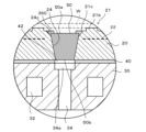
- the bottom 160a of the plug joint 160 which is a laser welded portion and has an inverted triangular cross section, is located at the boundary between the plug 50 and the plug arrangement hole 24, but this is not particularly limited.
- the bottom 560a of the plug joint 560 may be located on the plug 50 side.
- the same symbols are used for the same configuration as in the second embodiment.
- the laser irradiation position in the process of forming the plug joint 560 is on the plug side. Therefore, even if laser irradiation is performed, cracks are unlikely to occur in the ceramic plate 20. If a crack occurs in the ceramic plate 20, the plug arrangement hole 24 and the electrode 22 may be connected by the crack, which is likely to cause a malfunction, but by adopting the configuration of FIG. 13, such malfunctions can be prevented.
- the outer peripheral surface of the plug 50 and the inner peripheral surface of the plug placement hole 24 may be brought into close contact with each other. This has the effect of suppressing discharge between the outer peripheral surface of the plug 50 and the inner peripheral surface of the plug placement hole 24 when plasma is generated.
- the present invention can be used for wafer placement stages used in semiconductor manufacturing equipment, such as ceramic heaters, electrostatic chuck heaters, and electrostatic chucks.
- 10 wafer mounting table 20 ceramic plate, 21 wafer mounting surface, 21a seal band, 21b small circular protrusion, 21c reference surface, 22 electrode, 24 plug placement hole, 24c placement hole inclined surface, 30 base plate, 32 coolant flow path, 34 gas hole, 34a large diameter portion, 40 metal bonding layer, 42 through hole, 50 plug, 50a upper surface, 50b lower surface, 50c plug inclined surface, 64a ring portion, 64b introduction portion, 64c distribution portion, 90 metal bonding material, 92 through hole, 94 bonding body, 110, 210 wafer mounting table, 60, 160, 260, 360, 460, 466, 560 plug bonding portion, 160a, 560a bottom, W wafer.
Landscapes
- Physics & Mathematics (AREA)
- Engineering & Computer Science (AREA)
- Plasma & Fusion (AREA)
- Optics & Photonics (AREA)
- Chemical & Material Sciences (AREA)
- Analytical Chemistry (AREA)
- Mechanical Engineering (AREA)
- Container, Conveyance, Adherence, Positioning, Of Wafer (AREA)
Priority Applications (6)
| Application Number | Priority Date | Filing Date | Title |
|---|---|---|---|
| KR1020237032591A KR102721433B1 (ko) | 2023-02-27 | 2023-02-27 | 웨이퍼 적재대 |
| JP2023553025A JP7657310B2 (ja) | 2023-02-27 | 2023-02-27 | ウエハ載置台 |
| PCT/JP2023/007066 WO2024180611A1 (ja) | 2023-02-27 | 2023-02-27 | ウエハ載置台 |
| CN202380010192.1A CN120677559A (zh) | 2023-02-27 | 2023-02-27 | 晶片载放台 |
| US18/461,611 US12451385B2 (en) | 2023-02-27 | 2023-09-06 | Wafer placement table |
| TW112151302A TW202435355A (zh) | 2023-02-27 | 2023-12-28 | 晶圓載置台 |
Applications Claiming Priority (1)
| Application Number | Priority Date | Filing Date | Title |
|---|---|---|---|
| PCT/JP2023/007066 WO2024180611A1 (ja) | 2023-02-27 | 2023-02-27 | ウエハ載置台 |
Related Child Applications (1)
| Application Number | Title | Priority Date | Filing Date |
|---|---|---|---|
| US18/461,611 Continuation US12451385B2 (en) | 2023-02-27 | 2023-09-06 | Wafer placement table |
Publications (1)
| Publication Number | Publication Date |
|---|---|
| WO2024180611A1 true WO2024180611A1 (ja) | 2024-09-06 |
Family
ID=92461088
Family Applications (1)
| Application Number | Title | Priority Date | Filing Date |
|---|---|---|---|
| PCT/JP2023/007066 Ceased WO2024180611A1 (ja) | 2023-02-27 | 2023-02-27 | ウエハ載置台 |
Country Status (6)
| Country | Link |
|---|---|
| US (1) | US12451385B2 (https=) |
| JP (1) | JP7657310B2 (https=) |
| KR (1) | KR102721433B1 (https=) |
| CN (1) | CN120677559A (https=) |
| TW (1) | TW202435355A (https=) |
| WO (1) | WO2024180611A1 (https=) |
Families Citing this family (1)
| Publication number | Priority date | Publication date | Assignee | Title |
|---|---|---|---|---|
| WO2025134287A1 (ja) * | 2023-12-20 | 2025-06-26 | 日本碍子株式会社 | 半導体製造装置用部材 |
Citations (8)
| Publication number | Priority date | Publication date | Assignee | Title |
|---|---|---|---|---|
| US20020135969A1 (en) * | 1996-04-26 | 2002-09-26 | Applied Materials, Inc. | Electrostatic chuck having composite dielectric layer and method of manufacture |
| US6581275B2 (en) * | 2001-01-22 | 2003-06-24 | Applied Materials Inc. | Fabricating an electrostatic chuck having plasma resistant gas conduits |
| JP2006344766A (ja) * | 2005-06-09 | 2006-12-21 | Matsushita Electric Ind Co Ltd | プラズマ処理装置 |
| JP2010123712A (ja) * | 2008-11-19 | 2010-06-03 | Nihon Ceratec Co Ltd | 静電チャックおよびその製造方法 |
| WO2020004478A1 (ja) * | 2018-06-29 | 2020-01-02 | 北陸成型工業株式会社 | 静電チャック |
| WO2020121898A1 (ja) * | 2018-12-14 | 2020-06-18 | 日本発條株式会社 | 流路付きプレート |
| JP2020145280A (ja) * | 2019-03-05 | 2020-09-10 | Toto株式会社 | 静電チャック |
| JP2023003957A (ja) * | 2021-06-25 | 2023-01-17 | 東京エレクトロン株式会社 | プラズマ処理装置及び基板支持部 |
Family Cites Families (10)
| Publication number | Priority date | Publication date | Assignee | Title |
|---|---|---|---|---|
| US5539609A (en) * | 1992-12-02 | 1996-07-23 | Applied Materials, Inc. | Electrostatic chuck usable in high density plasma |
| US11227749B2 (en) * | 2016-02-18 | 2022-01-18 | Lam Research Corporation | 3D printed plasma arrestor for an electrostatic chuck |
| JP6767829B2 (ja) | 2016-09-27 | 2020-10-14 | 日本特殊陶業株式会社 | 対象物載置用部材 |
| JP6865145B2 (ja) * | 2016-12-16 | 2021-04-28 | 日本特殊陶業株式会社 | 保持装置 |
| JP6994981B2 (ja) | 2018-02-26 | 2022-01-14 | 東京エレクトロン株式会社 | プラズマ処理装置及び載置台の製造方法 |
| US20200411355A1 (en) | 2019-06-28 | 2020-12-31 | Applied Materials, Inc. | Apparatus for reduction or prevention of arcing in a substrate support |
| JP7299805B2 (ja) * | 2019-09-09 | 2023-06-28 | 日本特殊陶業株式会社 | 保持装置 |
| JP7600025B2 (ja) * | 2021-04-23 | 2024-12-16 | 新光電気工業株式会社 | 静電吸着部材及び基板固定装置 |
| JP7255659B1 (ja) * | 2021-11-25 | 2023-04-11 | 住友大阪セメント株式会社 | 静電チャック装置 |
| JP7560675B1 (ja) * | 2022-12-05 | 2024-10-02 | 日本碍子株式会社 | 半導体製造装置用部材 |
-
2023
- 2023-02-27 WO PCT/JP2023/007066 patent/WO2024180611A1/ja not_active Ceased
- 2023-02-27 CN CN202380010192.1A patent/CN120677559A/zh active Pending
- 2023-02-27 KR KR1020237032591A patent/KR102721433B1/ko active Active
- 2023-02-27 JP JP2023553025A patent/JP7657310B2/ja active Active
- 2023-09-06 US US18/461,611 patent/US12451385B2/en active Active
- 2023-12-28 TW TW112151302A patent/TW202435355A/zh unknown
Patent Citations (8)
| Publication number | Priority date | Publication date | Assignee | Title |
|---|---|---|---|---|
| US20020135969A1 (en) * | 1996-04-26 | 2002-09-26 | Applied Materials, Inc. | Electrostatic chuck having composite dielectric layer and method of manufacture |
| US6581275B2 (en) * | 2001-01-22 | 2003-06-24 | Applied Materials Inc. | Fabricating an electrostatic chuck having plasma resistant gas conduits |
| JP2006344766A (ja) * | 2005-06-09 | 2006-12-21 | Matsushita Electric Ind Co Ltd | プラズマ処理装置 |
| JP2010123712A (ja) * | 2008-11-19 | 2010-06-03 | Nihon Ceratec Co Ltd | 静電チャックおよびその製造方法 |
| WO2020004478A1 (ja) * | 2018-06-29 | 2020-01-02 | 北陸成型工業株式会社 | 静電チャック |
| WO2020121898A1 (ja) * | 2018-12-14 | 2020-06-18 | 日本発條株式会社 | 流路付きプレート |
| JP2020145280A (ja) * | 2019-03-05 | 2020-09-10 | Toto株式会社 | 静電チャック |
| JP2023003957A (ja) * | 2021-06-25 | 2023-01-17 | 東京エレクトロン株式会社 | プラズマ処理装置及び基板支持部 |
Also Published As
| Publication number | Publication date |
|---|---|
| US12451385B2 (en) | 2025-10-21 |
| CN120677559A (zh) | 2025-09-19 |
| KR20240134715A (ko) | 2024-09-10 |
| TW202435355A (zh) | 2024-09-01 |
| US20240290646A1 (en) | 2024-08-29 |
| KR102721433B1 (ko) | 2024-10-25 |
| JPWO2024180611A1 (https=) | 2024-09-06 |
| JP7657310B2 (ja) | 2025-04-04 |
Similar Documents
| Publication | Publication Date | Title |
|---|---|---|
| KR102755205B1 (ko) | 반도체 제조 장치용 부재 | |
| JP7620578B2 (ja) | 半導体製造装置用部材 | |
| JP7569343B2 (ja) | 半導体製造装置用部材 | |
| US12211729B2 (en) | Member for semiconductor manufacturing apparatus | |
| JP7483121B2 (ja) | 半導体製造装置用部材 | |
| KR20230053499A (ko) | 웨이퍼 배치대 | |
| TWI849797B (zh) | 晶圓載置台 | |
| KR20230095821A (ko) | 반도체 제조 장치용 부재 | |
| JP7657310B2 (ja) | ウエハ載置台 | |
| KR102690180B1 (ko) | 웨이퍼 배치대 | |
| TWI875257B (zh) | 晶圓載置台 | |
| JP7751079B2 (ja) | 半導体製造装置用部材 | |
| JP7503708B1 (ja) | 半導体製造装置用部材 | |
| JP7780062B1 (ja) | ウエハ載置台 | |
| CN119968700A (zh) | 晶片载放台 | |
| JP7691578B1 (ja) | 半導体製造装置用部材 | |
| US20250079229A1 (en) | Wafer placement table |
Legal Events
| Date | Code | Title | Description |
|---|---|---|---|
| WWE | Wipo information: entry into national phase |
Ref document number: 202380010192.1 Country of ref document: CN |
|
| WWE | Wipo information: entry into national phase |
Ref document number: 2023553025 Country of ref document: JP |
|
| 121 | Ep: the epo has been informed by wipo that ep was designated in this application |
Ref document number: 23925169 Country of ref document: EP Kind code of ref document: A1 |
|
| WWP | Wipo information: published in national office |
Ref document number: 202380010192.1 Country of ref document: CN |
|
| NENP | Non-entry into the national phase |
Ref country code: DE |
|
| 122 | Ep: pct application non-entry in european phase |
Ref document number: 23925169 Country of ref document: EP Kind code of ref document: A1 |