WO2024176856A1 - 2回回転水晶振動板 - Google Patents
2回回転水晶振動板 Download PDFInfo
- Publication number
- WO2024176856A1 WO2024176856A1 PCT/JP2024/004275 JP2024004275W WO2024176856A1 WO 2024176856 A1 WO2024176856 A1 WO 2024176856A1 JP 2024004275 W JP2024004275 W JP 2024004275W WO 2024176856 A1 WO2024176856 A1 WO 2024176856A1
- Authority
- WO
- WIPO (PCT)
- Prior art keywords
- vibration
- quartz crystal
- axis
- axis direction
- plate
- Prior art date
- Legal status (The legal status is an assumption and is not a legal conclusion. Google has not performed a legal analysis and makes no representation as to the accuracy of the status listed.)
- Ceased
Links
Images







Classifications
-
- H—ELECTRICITY
- H03—ELECTRONIC CIRCUITRY
- H03H—IMPEDANCE NETWORKS, e.g. RESONANT CIRCUITS; RESONATORS
- H03H9/00—Networks comprising electromechanical or electro-acoustic elements; Electromechanical resonators
- H03H9/15—Constructional features of resonators consisting of piezoelectric or electrostrictive material
- H03H9/17—Constructional features of resonators consisting of piezoelectric or electrostrictive material having a single resonator
- H03H9/19—Constructional features of resonators consisting of piezoelectric or electrostrictive material having a single resonator consisting of quartz
Definitions
- the present invention relates to a two-rotation quartz crystal plate.
- a twice-rotated quartz crystal vibration plate for example an SC-cut quartz crystal vibration plate
- a twice-rotated quartz crystal vibration plate has an X-axis and a Z-axis along a plane perpendicular to the Y-axis, which is the crystal axis of the quartz crystal, and is formed by cutting out from a plane along the Z'-axis and X'-axis, with the Z'-axis being the axis obtained by rotating the Z-axis around the X-axis, and the X'-axis being the axis obtained by rotating the X-axis around the Z-axis.
- the main vibration fundamental wave
- C-mode vibration thinness-shear vibration
- B-mode vibration thinness-twist vibration
- the present invention was made in consideration of the above-mentioned circumstances, and aims to provide a two-rotation quartz crystal plate that can efficiently suppress B-mode vibration with a simple structure.
- the present invention provides a means for solving the above-mentioned problems as follows. That is, the present invention provides a twice-rotated quartz crystal plate cut from a plane along the Z' and X' axes, with an X-axis and Z-axis along a plane perpendicular to the Y-axis, which is the crystal axis of the quartz crystal, the Z'-axis being the axis obtained by rotating the Z-axis around the X-axis, and the X'-axis being the axis obtained by rotating the X-axis around the Z-axis, and the plate includes a vibration part having excitation electrodes formed on the front and back surfaces, and an outer frame part provided on the outer periphery of the vibration part, a through-hole is provided between the vibration part and the outer frame part in the thickness direction, the vibration part and the outer frame part are connected at the end of the vibration part in the X'-axis direction perpendicular to the Z'-axis by a holding part extending in
- the above configuration allows for efficient suppression of B-mode vibrations with a simple structure in which end electrodes are provided at the ends of the vibration section in the Z'-axis direction.
- the ends of both main surfaces of the vibration section in the Z'-axis direction which are at the same potential due to the end electrodes, act to cancel out the potential difference caused by the thickness torsion vibration of B-mode, thereby weakening the vibration strength of B-mode.
- the holding section extending in the Z'-axis direction can suppress B-mode vibrations. This allows for accurate detection of C-mode vibrations, which have a high vibration component in the X'-axis direction, and allows for oscillation at the frequency of only the main vibration of C-mode.
- the end electrode is adjacent to the holding portion.
- the holding portion and the end electrode are adjacent to each other along the X'-axis direction, so that the vibration of B mode can be efficiently suppressed without unnecessarily expanding the vibration portion.
- the end electrodes are provided on both of the opposing sides in the X'-axis direction of the vibration part.
- the end electrodes increase the electric field-free solution area at the same potential, making it possible to efficiently suppress B-mode vibration.
- the excitation electrode reaches the area of the holding part in the X'-axis direction.
- This configuration is desirable for suppressing B-mode vibration, and ensures the area of the excitation electrode within the limited size of the vibration part, thereby improving electrical characteristics such as the CI value of C-mode.
- the length of the end electrode in the X'-axis direction is equal to or greater than the length of the excitation electrode in the X'-axis direction, and that the end electrode and the excitation electrode overlap in the Z'-axis direction.
- the vibration part is shaped so that the thickness at both ends in the Z'-axis direction becomes thinner toward the ends. This configuration makes it difficult for secondary vibrations (such as contour or flexural vibrations) generated in the vibration part to couple with C-mode vibrations caused by thickness-slip vibrations.
- the inner ends of the end electrodes are provided at positions that are approximately aligned on the front and back surfaces of the vibration section.
- the holding portion does not extend in the X'-axis direction relative to the excitation electrode.
- the end of the vibration portion in the X'-axis direction is a free end, so that the vibration portion can be made compact without adversely affecting the C-mode vibration.
- a protrusion protruding in the thickness direction of the vibration part is formed at the end of the vibration part, and the end electrode is formed so as to cover the protrusion.
- the end electrode can form an electric field-free area at the end of the vibration part, making it possible to cancel B-mode vibration.
- by providing a protrusion at the end of the vibration part and forming an inclined surface on the protrusion it is possible to suppress B-mode vibration. Therefore, with this configuration, a synergistic effect can be obtained in terms of suppressing B-mode vibration.
- B-mode vibration can be efficiently suppressed by a simple structure in which an end electrode is provided at the end of the vibrating part in the Z'-axis direction.
- FIG. 1 is a schematic diagram showing a crystal unit including a crystal plate according to the present embodiment.
- FIG. 2 is a schematic plan view of a first main surface side of a first sealing member provided in the quartz crystal unit.
- FIG. 3 is a schematic plan view of the second main surface side of the first sealing member provided in the quartz crystal unit.
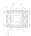
- FIG. 4 is a schematic plan view of the first main surface side of the quartz crystal plate according to this embodiment.
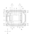
- FIG. 5 is a schematic plan view of the second main surface side of the quartz crystal plate according to this embodiment.
- FIG. 6 is a schematic plan view of the first main surface side of the second sealing member provided in the quartz crystal unit.
- FIG. 7 is a schematic plan view of the second main surface side of the second sealing member provided in the quartz crystal unit.
- FIG. 1 is a schematic diagram showing a crystal unit including a crystal plate according to the present embodiment.
- FIG. 2 is a schematic plan view of a first main surface side of a first sealing member provided in the quartz crystal unit.
- FIG. 8 is a cross-sectional view taken along line A1-A1 in FIG.
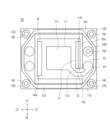
- FIG. 9 is a view equivalent to FIG. 4 of a quartz crystal plate according to another embodiment 1.
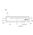
- FIG. 10 is a view corresponding to FIG. 8 of a quartz crystal plate according to another embodiment 2.
- FIG. 11 is a schematic diagram showing a first modified example of a quartz crystal resonator.
- FIG. 12 is a cross-sectional view taken along line A2-A2 in FIG.
- FIG. 13 is a view corresponding to FIG. 12 and showing a second modified example of the quartz crystal resonator.
- the quartz crystal vibrator 100 is configured to include the quartz crystal vibration plate 10, a first sealing member 20, and a second sealing member 30.
- the quartz crystal vibration plate 10 and the first sealing member 20 are bonded together, and the quartz crystal vibration plate 10 and the second sealing member 30 are bonded together to form a package having a substantially rectangular sandwich structure.
- the first sealing member 20 and the second sealing member 30 are bonded to each of the two main surfaces of the quartz crystal vibration plate 10 to form an internal space (cavity) of the package, and the vibration part 11 (see FIG. 4 and FIG. 5) is hermetically sealed in this internal space.
- the crystal unit 100 has a package size of, for example, 1.0 x 0.8 mm, and is designed to be compact and low-profile.
- the crystal unit 100 is electrically connected via solder to an external circuit board (not shown) that is provided externally.
- Figs. 1 to 7 merely show one configuration example of the quartz crystal plate 10, the first sealing member 20, and the second sealing member 30, respectively, and do not limit the present invention.
- the quartz vibration plate 10 is a piezoelectric substrate made of quartz, and both of its main surfaces (first main surface 101, second main surface 102) are formed as flat and smooth surfaces (mirror finish).
- a twice-rotated quartz vibration plate is used as the quartz vibration plate 10, and more specifically, an SC-cut quartz plate is used.
- both main surfaces 101, 102 of the quartz vibration plate 10 are in the X'Z' plane.
- the direction parallel to the short side direction (short side direction) of the quartz vibration plate 10 is the X' axis direction
- the direction parallel to the long side direction (long side direction) of the quartz vibration plate 10 is the Z' axis direction.
- SC cut is a processing technique in which, for example, a plane perpendicular to the Y axis of the three crystal axes of quartz, the electric axis (X axis), the mechanical axis (Y axis), and the optical axis (Z axis), is rotated around the X axis by a predetermined angle (e.g., 33.5° or 34.0°), and then cut out from a plane rotated a predetermined angle (e.g., 21° or 22°) around the Z axis from this rotated position.
- a predetermined angle e.g., 33.5° or 34.0°
- the X'-axis and Z'-axis directions shown in Figures 4 and 5 are the cutting directions when cutting out the SC-cut quartz plate (the directions of the crystal axes after the above two rotations) (the same applies to the Y axis direction).
- the above-mentioned cutting angle is an example, and other angles may be used within the range of typical SC cut cutting angles.
- the angle at which the plane perpendicular to the Y axis is rotated around the X axis can be about 33° to 35°
- the angle at which it is rotated around the Z axis from this rotated position can be about 22° to 24°.
- a pair of excitation electrodes (first excitation electrode 111, second excitation electrode 112) are formed on both main surfaces 101, 102 of the quartz vibration plate 10.
- the quartz vibration plate 10 has a vibration part 11 formed in a substantially rectangular shape, an outer frame part 12 surrounding the outer periphery of the vibration part 11, and a holding part 13 that holds the vibration part 11 by connecting the vibration part 11 and the outer frame part 12.
- the quartz vibration plate 10 is configured such that the vibration part 11, the outer frame part 12, and the holding part 13 are integrally provided.
- the holding part 13 extends (protrudes) from only one corner of the vibration part 11 located in the +X' direction and the -Z' direction to the outer frame part 12 in the -Z direction.
- a through part (slit) 10a is formed between the vibration part 11 and the outer frame part 12.
- the quartz crystal vibration plate 10 is provided with only one holding portion 13 that connects the vibration portion 11 and the outer frame portion 12, and the through portion 10a is formed continuously so as to surround the outer periphery of the vibration portion 11.
- the first excitation electrode 111 is provided on the first main surface 101 side of the vibration part 11, and the second excitation electrode 112 is provided on the second main surface 102 side of the vibration part 11.
- the first excitation electrode 111 and the second excitation electrode 112 are connected to lead-out wiring (first lead-out wiring 113, second lead-out wiring 114) for connecting these excitation electrodes to external electrode terminals.
- the first lead-out wiring 113 is led out from the first excitation electrode 111 and connected to the connection bonding pattern 14 formed on the outer frame part 12 via the holding part 13.
- the second lead-out wiring 114 is led out from the second excitation electrode 112 and connected to the connection bonding pattern 15 formed on the outer frame part 12 via the holding part 13.
- End electrodes 16 and 17 are formed on both ends of the vibration part 11 in the Z'-axis direction.
- the end electrodes 16 and 17 are disposed at a predetermined distance from the first excitation electrode 111 and the second excitation electrode 112, and are provided at positions sandwiching the first excitation electrode 111 and the second excitation electrode 112. Details of the end electrodes 16 and 17 will be described later.
- a diaphragm-side sealing portion is provided on each of the two main surfaces (first main surface 101, second main surface 102) of the quartz crystal vibration plate 10 for bonding the quartz crystal vibration plate 10 to the first sealing member 20 and the second sealing member 30.
- a diaphragm-side first bonding pattern 121 is formed as the diaphragm-side sealing portion on the first main surface 101
- a diaphragm-side second bonding pattern 122 is formed as the diaphragm-side sealing portion on the second main surface 102.
- the diaphragm-side first bonding pattern 121 and the diaphragm-side second bonding pattern 122 are provided on the outer frame portion 12 and are formed in a ring shape in a plan view.
- five through holes are formed in the quartz crystal vibration plate 10, penetrating between the first main surface 101 and the second main surface 102.
- the four first through holes 161 are provided in the four corner regions of the outer frame portion 12.
- the second through hole 162 is provided in the outer frame portion 12, on one side in the Z'-axis direction of the vibration portion 11 (the -Z' direction side in Figs. 4 and 5).
- a connection bonding pattern 123 is formed around each of the first through holes 161.
- a connection bonding pattern 124 is formed on the first main surface 101 side around the second through hole 162, and a connection bonding pattern 15 is formed on the second main surface 102 side around the second through hole 162.
- first through-hole 161 and the second through-hole 162 a through electrode for establishing electrical continuity between the electrodes formed on the first main surface 101 and the second main surface 102 is formed along the inner wall surface of each through-hole.
- the central portion of each of the first through-hole 161 and the second through-hole 162 is a hollow through portion penetrating between the first main surface 101 and the second main surface 102.
- the outer peripheral edge of the vibration plate side first bonding pattern 121 is provided close to the outer peripheral edge of the first main surface 101 of the quartz vibration plate 10 (outer frame portion 12).
- the outer peripheral edge of the vibration plate side second bonding pattern 122 is provided close to the outer peripheral edge of the second main surface 102 of the quartz vibration plate 10 (outer frame portion 12).
- the first sealing member 20 is a rectangular parallelepiped substrate formed from a single quartz plate, and the second main surface 202 (the surface that is bonded to the quartz plate 10) of the first sealing member 20 is formed as a flat and smooth surface (mirror finish).
- the first sealing member 20 does not have a vibrating part, by using an SC-cut quartz plate like the quartz plate 10, the thermal expansion coefficients of the quartz plate 10 and the first sealing member 20 can be made the same, and thermal deformation in the quartz unit 100 can be suppressed.
- the directions of the X'-axis, Y-axis, and Z'-axis in the first sealing member 20 are also the same as those of the quartz plate 10.
- the first sealing member 20 may be made of a quartz plate or glass with a cut angle other than SC cut (for example, AT cut) (the same applies to the second sealing member 30).
- the first main surface 201 (the outer main surface not facing the quartz crystal vibration plate 10) of the first sealing member 20 has first and second terminals 22, 23 for wiring and a metal film 28 for shielding (earth connection).
- the first and second terminals 22, 23 for wiring are provided as wiring for electrically connecting the first and second excitation electrodes 111, 112 of the quartz crystal vibration plate 10 to the external electrode terminal 32 of the second sealing member 30.
- the first and second terminals 22, 23 are provided at both ends in the Z'-axis direction, with the first terminal 22 provided on the +Z'-direction side and the second terminal 23 provided on the -Z'-direction side.
- the first and second terminals 22, 23 are formed to extend in the X'-axis direction.
- the first terminal 22 and the second terminal 23 are formed in an approximately rectangular shape.
- the metal film 28 is provided between the first and second terminals 22, 23, and is disposed at a predetermined distance from the first and second terminals 22, 23.
- the metal film 28 is provided in almost all areas of the first main surface 201 of the first sealing member 20 where the first and second terminals 22, 23 are not formed.
- the metal film 28 is provided from the end in the +X' direction to the end in the -X' direction of the first main surface 201 of the first sealing member 20.
- the first sealing member 20 has six through holes formed between the first main surface 201 and the second main surface 202. Specifically, four third through holes 211 are provided in the four corner (corner) areas of the first sealing member 20. The fourth and fifth through holes 212, 213 are provided in the +Z' and -Z' directions in Figures 2 and 3, respectively.
- a through electrode for establishing electrical continuity between the electrodes formed on the first main surface 201 and the second main surface 202 is formed along the inner wall surface of each through hole.
- the central portion of each of the third through hole 211 and the fourth and fifth through holes 212, 213 is a hollow through portion penetrating between the first main surface 201 and the second main surface 202.
- the through electrodes of the two third through holes 211, 211 diagonally positioned on the first main surface 201 of the first sealing member 20 are electrically connected to each other by the metal film 28.
- the through electrode of the third through hole 211 located at the corner in the -X' direction and the +Z' direction and the through electrode of the fourth through hole 212 are electrically connected by the first terminal 22.
- the through electrode of the third through hole 211 located at the corner in the +X' direction and the -Z' direction and the through electrode of the fifth through hole 213 are electrically connected by the second terminal 23.
- the second main surface 202 of the first sealing member 20 is formed with a sealing member side first bonding pattern 24 as a sealing member side first sealing part for bonding to the quartz crystal vibration plate 10.
- the sealing member side first bonding pattern 24 is formed in a ring shape in a plan view.
- a connection bonding pattern 25 is formed around each of the third through holes 211.
- a connection bonding pattern 261 is formed around the fourth through hole 212, and a connection bonding pattern 262 is formed around the fifth through hole 213.
- connection bonding pattern 263 is formed on the opposite side (-Z' direction side) of the long axis direction of the first sealing member 20 from the connection bonding pattern 261, and the connection bonding pattern 261 and the connection bonding pattern 263 are connected by a wiring pattern 27.
- the outer periphery of the sealing member side first bonding pattern 24 is provided close to the outer periphery of the second main surface 202 of the first sealing member 20.
- the second sealing member 30 is a rectangular parallelepiped substrate formed from a single quartz plate, and the first main surface 301 (the surface that is bonded to the quartz vibration plate 10) of this second sealing member 30 is formed as a flat and smooth surface (mirror finish). Note that, like the quartz vibration plate 10, the second sealing member 30 also uses an SC cut quartz plate, and it is desirable that the orientation of the X' axis, Y axis, and Z' axis is the same as that of the quartz vibration plate 10.
- a sealing member-side second bonding pattern 31 is formed on the first main surface 301 of the second sealing member 30 as a sealing member-side second sealing portion for bonding to the quartz crystal vibration plate 10.
- the sealing member-side second bonding pattern 31 is formed in a ring shape in a plan view.
- the outer peripheral edge of the sealing member-side second bonding pattern 31 is provided close to the outer peripheral edge of the first main surface 301 of the second sealing member 30.
- External electrode terminals 32 are provided on the second main surface 302 (the outer main surface that does not face the quartz crystal plate 10) of the second sealing member 30, which are electrically connected to an external circuit board provided outside the quartz crystal unit 100.
- the external electrode terminals 32 are located at the four corners (corner portions) of the second main surface 302 of the second sealing member 30.
- the second sealing member 30 has four through holes that penetrate between the first main surface 301 and the second main surface 302.
- the four sixth through holes 33 are provided in the four corner (corner) regions of the second sealing member 30.
- a through electrode for achieving electrical continuity between the electrodes formed on the first main surface 301 and the second main surface 302 is formed along the inner wall surface of each sixth through hole 33.
- the through electrode formed on the inner wall surface of the sixth through hole 33 provides electrical continuity between the electrode formed on the first main surface 301 and the external electrode terminal 32 formed on the second main surface 302.
- the center portion of each sixth through hole 33 is a hollow through portion that penetrates between the first main surface 301 and the second main surface 302.
- a connection bonding pattern 34 is formed around each of the sixth through holes 33.
- the quartz crystal vibration plate 10 and the first sealing member 20 are diffusion bonded with the diaphragm-side first bonding pattern 121 and the sealing member-side first bonding pattern 24 overlapping each other, and the quartz crystal vibration plate 10 and the second sealing member 30 are diffusion bonded with the diaphragm-side second bonding pattern 122 and the sealing member-side second bonding pattern 31 overlapping each other, to produce a sandwich-structured package as shown in FIG. 1.
- connection bonding patterns are also diffusion bonded in a state of being superimposed.
- electrical conduction is obtained between the first excitation electrode 111, the second excitation electrode 112, and the external electrode terminal 32 in the quartz crystal resonator 100.
- the first excitation electrode 111 is connected to the external electrode terminal 32 via the first lead-out wiring 113, the wiring pattern 27, the fourth through hole 212, the first terminal 22, the third through hole 211, the first through hole 161, and the sixth through hole 33 in this order.
- the second excitation electrode 112 is connected to the external electrode terminal 32 via the second lead-out wiring 114, the second through hole 162, the fifth through hole 213, the second terminal 23, the third through hole 211, the first through hole 161, and the sixth through hole 33 in this order.
- the metal film 28 is connected to earth (ground connection, using part of the external electrode terminal 32) via the third through hole 211, the first through hole 161, and the sixth through hole 33 in that order.
- the various bonding patterns are preferably formed by stacking multiple layers on the quartz crystal plate, with a Ti (titanium) layer and an Au (gold) layer formed from the bottom layer onwards by deposition or sputtering.
- the bonding patterns, wiring and electrodes can be patterned simultaneously, which is preferable.
- the sealing portions (seal paths) 115, 116 that hermetically seal the vibration portion 11 of the quartz crystal vibrating plate 10 are formed in an annular shape in a plan view.
- the seal path 115 is formed by diffusion bonding (Au-Au bonding) of the above-mentioned vibration plate side first bonding pattern 121 and the sealing member side first bonding pattern 24, and the outer and inner edge shapes of the seal path 115 are formed in a substantially octagonal shape.
- the seal path 116 is formed by diffusion bonding (Au-Au bonding) of the above-mentioned vibration plate side second bonding pattern 122 and the sealing member side second bonding pattern 31, and the outer and inner edge shapes of the seal path 116 are formed in a substantially octagonal shape.
- the first sealing member 20 and the quartz crystal plate 10 have a gap of 1.00 ⁇ m or less
- the second sealing member 30 and the quartz crystal plate 10 have a gap of 1.00 ⁇ m or less.
- the thickness of the seal path 115 between the first sealing member 20 and the quartz crystal plate 10 is 1.00 ⁇ m or less
- the thickness of the seal path 116 between the second sealing member 30 and the quartz crystal plate 10 is 1.00 ⁇ m or less (specifically, 0.15 ⁇ m to 1.00 ⁇ m for the Au-Au bonding of this embodiment).
- the thickness of a conventional metal paste sealing material using Sn is 5 ⁇ m to 20 ⁇ m.
- a through-hole 10a is provided between the vibration part 11 and the outer frame part 12, penetrating the quartz crystal vibration plate 10 in the thickness direction, the vibration part 11 and the outer frame part 12 are connected at the end of the vibration part 11 in the X'-axis direction perpendicular to the Z'-axis by a holding part 13 extending in the Z'-axis direction, and the vibration part 11 has end electrodes 16, 17 formed along opposing sides extending in the X'-axis direction of the vibration part 11, which make the ends of both main surfaces 101, 102 of the vibration part 11 at the same potential.
- the vibration part 11 has inclined surfaces 11a and 11b formed at both ends in the Z'-axis direction, which are inclined with respect to the vibration plane of the vibration part 11.
- the inclined surfaces 11a and 11b are formed during wet etching of the quartz crystal vibration plate 10 due to the anisotropy of quartz crystal.
- the cross-sectional shape of the vibration part 11 cut in the Z'Y plane is a parallelogram.
- the side surface on the +Z' direction side of the vibration part 11 is the inclined surface 11a that is inclined at a predetermined angle with respect to the vibration plane of the vibration part 11, and the side surface on the -Z' direction side of the vibration part 11 is the inclined surface 11b that is inclined at approximately the same angle as the inclined surface 11a.
- the inclined surfaces 11a and 11b may be inclined at different angles.
- the inclined surfaces 11a and 11b may also be inclined surfaces that have a curved slope, stepped slopes, or slopes that have a minute bend.
- an end electrode 16 is formed on the end of the vibration part 11 on the +Z' direction side, and an end electrode 17 is formed on the end of the vibration part 11 on the -Z' direction side.
- the end electrode 16 is configured such that an approximately rectangular first portion 16a is formed on the surface (first main surface 101) of the end of the vibration part 11 on the +Z' direction side, an approximately rectangular second portion 16b is formed on the back surface (second main surface 102) of the end, and an approximately rectangular third portion 16c is formed on the side surface (inclined surface 11a).
- the end electrode 17 is configured such that an approximately rectangular first portion 17a is formed on the surface (first main surface 101) of the end of the vibration part 11 on the -Z' direction side, an approximately rectangular second portion 17b is formed on the back surface (second main surface 102), and an approximately rectangular third portion 17c is formed on the side surface (inclined surface 11b).
- the end electrodes 16, 17 are formed to the same thickness as the first and second excitation electrodes 111, 112.
- the end electrodes 16, 17 are preferably formed from a metal material that is a conductor and has low electrical resistance. In this case, the end electrodes 16, 17 are formed from the same material as the first and second excitation electrodes 111, 112.
- the end electrodes 16, 17 are formed together with the first and second excitation electrodes 111, 112, the first and second lead wirings 113, 114, etc., by performing sputtering and photolithography on the quartz crystal vibration plate 10 in which the vibration portion 11, the outer frame portion 12, the through portion 10a, etc. are formed by wet etching.
- the end electrodes 16, 17 are not electrically connected to the first and second excitation electrodes 111, 112, and are provided electrically independent of the first and second excitation electrodes 111, 112.
- the end electrodes 16 and 17 may be formed from a material different from that of the first and second excitation electrodes 111 and 112.
- the thickness of the end electrodes 16 and 17 may be made larger than the thickness of the first and second excitation electrodes 111 and 112 to reduce the electrical resistance of the end electrodes 16 and 17.
- the first portion 16a of the end electrode 16 and the end (inner end) of the second portion 16b on the -Z' direction side are provided at approximately the same position.
- the first portion 17a of the end electrode 17 and the end (inner end) of the second portion 17b on the +Z' direction side are provided at approximately the same position.
- the first portion 16a of the end electrode 16 and the first excitation electrode 111 are arranged at a predetermined distance L1
- the second portion 16b of the end electrode 16 and the second excitation electrode 112 are arranged at the same distance L1.
- the first portion 17a of the end electrode 17 and the first excitation electrode 111 are arranged at a predetermined distance L2, and the second portion 17b of the end electrode 17 and the second excitation electrode 112 are arranged at the same distance L2.
- the distances L1 and L2 are set to approximately the same size.
- the distances L1 and L2 are set based on the size of the vibration part 11, the size of the first and second excitation electrodes 111 and 112, etc.
- the end electrodes 16, 17 are provided at positions sandwiching the first and second excitation electrodes 111, 112 in a plan view.
- the end electrodes 16, 17 are provided along opposing sides extending in the X'-axis direction of the vibration part 11.
- the first part 16a of the end electrode 16 and the first part 17a of the end electrode 17 have approximately the same length in the X'-axis direction.
- the second part 16b of the end electrode 16 and the second part 17b of the end electrode 17 have approximately the same length in the X'-axis direction.
- the end electrode 17 is provided adjacent to the holding part 13, and the end of the end electrode 17 on the +X' direction side reaches the holding part 13.
- the quartz crystal vibration plate 10 can efficiently suppress the vibration of the B mode with a simple structure in which the end electrodes 16, 17 are provided at the ends of the vibration part 11 in the Z' axis direction.
- the ends of the main surfaces 101, 102 of the vibration part 11 in the Z' axis direction which are made to have the same potential by the end electrodes 16, 17, act to cancel the potential difference caused by the thickness torsion vibration of the B mode, and the vibration intensity of the B mode can be weakened.
- the vibration of the B mode can be mechanically suppressed by the holding part 13 extending in the Z' axis direction. This makes it possible to accurately detect the vibration of the C mode, which has a high vibration component in the X' axis direction, and to oscillate at the frequency of only the C mode of the main vibration.
- the vibration of the B-mode can be efficiently suppressed without unnecessarily expanding the vibration portion 11. Furthermore, since the end electrodes 16, 17 are provided on both of the opposing sides of the vibration portion 11 in the X'-axis direction, the electric field-free region that is at the same potential due to the end electrodes 16, 17 becomes larger, and the vibration of the B-mode can be efficiently suppressed.
- the first and second excitation electrodes 111, 112 reach (protrude) into the area of the holding portion 13 in the X'-axis direction, and the ends of the first and second excitation electrodes 111, 112 on the X'-axis side overlap with a part of the holding portion 13 in the Z'-axis direction.
- This is desirable for suppressing B-mode vibration, and it is possible to ensure the area of the first and second excitation electrodes 111, 112 within the limited size of the vibration portion 11, and improve electrical characteristics such as the CI value of C-mode.
- only one holding portion 13 is provided, it is possible to achieve a configuration that suppresses B-mode vibration and does not adversely affect C-mode vibration.
- the vibration of B mode can be effectively suppressed by setting the above-mentioned intervals L1, L2 to, for example, 20 ⁇ m to 30 ⁇ m.
- the intervals L1, L2 are made large, there is a problem that the effect of suppressing B mode is reduced. Also, if the intervals L1, L2 are made small, there is a problem that it also has an adverse effect on C mode.
- the cross-sectional shape of the vibration part 11 is a parallelogram, and the thickness of both ends of the vibration part 11 in the Z'-axis direction is thinner toward the ends. This makes it difficult for secondary vibrations (such as vibrations of a contour system or a bending system) generated in the vibration part 11 to be coupled with the C-mode vibration due to thickness-slip vibration.
- the inner ends of the end electrodes 16 and 17 are provided at positions that are approximately aligned on both main surfaces (the first main surface 101 and the second main surface 102) of the vibration part 11, it is possible to reliably form a field-free region without unnecessarily expanding the end electrodes 16 and 17, and to efficiently suppress the B-mode vibration.
- the holding part 13 is configured not to extend in the X'-axis direction relative to the first and second excitation electrodes 111 and 112, and the ends of the vibration part 11 in the X'-axis direction are free ends, it is possible to miniaturize the vibration part 11 while not adversely affecting the C-mode vibration.
- the first and second outgoing wirings 113 and 114 are configured not to extend in the X'-axis direction relative to the first and second excitation electrodes 111 and 112, so that the weighting of the first and second outgoing wirings 113 and 114 does not adversely affect the vibration in C mode.
- the length in the X'-axis direction of the end electrodes 16, 17 is smaller than the length in the X'-axis direction of the first and second excitation electrodes 111, 112, but this is not limited thereto, and the length in the X'-axis direction of the end electrodes 16, 17 may be equal to or greater than the length in the X'-axis direction of the first and second excitation electrodes 111, 112, as shown in FIG. 9, for example.
- the lengths in the X'-axis direction of the end electrodes 16, 17 may be the same or different.
- the length of the end electrode 16 in the X'-axis direction is equal to or greater than the length of the first and second excitation electrodes 111, 112 in the X'-axis direction, and that the end electrode 16 and the first and second excitation electrodes 111, 112 overlap in the Z'-axis direction.
- the end electrode 16 may be formed on the entirety of the opposing sides in the X'-axis direction of the vibration part 11 on the side on which the holding part 13 is not provided.
- the holding portion 13 and the end electrode 17 on the -Z' direction side of the vibration portion 11 are provided adjacent to each other (continuously), but this is not limited thereto, and a predetermined distance may be provided between the holding portion 13 and the end electrode 17.
- the end electrodes 16, 17 may be formed to reach the corners of the vibration portion 11.
- the noise can be reduced by connecting the end electrodes 16 and 17 to ground, but this is not limited thereto.
- the end electrodes 16 and 17 may be floating electrodes that are not connected to any electrode or wiring, or may be electrodes charged to a fixed positive or negative potential, as long as the ends in the Z'-axis direction of both main surfaces 101 and 102 of the vibration part 11 can be at the same potential.
- the end electrodes 16 and 17 are configured such that the first parts 16a and 17a and the second parts 16b and 17b are electrically connected via the third parts 16c and 17c, but the third parts 16c and 17c may be omitted, and the first parts 16a and 17a and the second parts 16b and 17b may be electrically connected by means of wires or the like.
- the end electrodes 16 and 17 may have different potentials, or may have the same potential.
- these end electrodes 16 and 17 may be used to adjust the electrical characteristics of the quartz crystal plate 10, such as the frequency, by increasing or decreasing the film thickness of the electrodes (for example, by ion milling or partial milling).
- end electrodes 16, 17 are provided on both opposing sides of the vibrating part 11 extending in the X'-axis direction, but an end electrode may be provided on only one side.
- an end electrode is provided on only one side, it is preferable to provide the end electrode on the opposing side of the vibrating part 11 in the X'-axis direction on the side on which the holding part 13 is not provided.
- the end electrode 16 may be formed continuously from one end to the other end of the side of the vibrating part 11 on which the holding part 13 is not provided.
- the cross-sectional shape of the vibration part 11 is a parallelogram, but the cross-sectional shape of the vibration part 11 is not particularly limited as long as the ends in the Z'-axis direction of both main surfaces 101, 102 of the vibration part 11 can be at the same potential.
- the cross-sectional shape of the vibration part 11 may be rectangular, or may have a protrusion 11c as shown in FIG. 10.
- a protrusion 11c that protrudes in the thickness direction of the vibration part 11 is formed at the end of the vibration part 11, and an end electrode 17 is formed to cover the protrusion 11c.
- the cross-sectional shape of the vibration part 11 shown in FIG. 10 is substantially the same as the shape shown in FIG. 8 of the above-mentioned Patent Document 1.
- a protrusion 11c is provided at the end of the vibration part 11 in the -Z' direction, and an inclined surface 11d is formed on the protrusion 11c, thereby suppressing B-mode vibration.
- the quartz vibration plate 10 shown in FIG. 10 is a modified example in which the end electrode of the above-mentioned embodiment is applied to the quartz vibration plate described in Patent Document 1.
- the end electrode 16 on the +Z' direction side of the vibrating part 11 has the same configuration as in the above embodiment, but the end electrode 17 on the -Z' direction side of the vibrating part 11 is provided so as to entirely cover the protrusion 11c.
- the end electrode 17 forms a portion at the end on the -Z' direction side of the vibrating part 11 where both main surfaces 101, 102 of the vibrating part 11 have the same potential.
- the inclined surface 11d of the protrusion 11c also has the effect of suppressing the B-mode vibration. In this way, a synergistic effect is obtained in terms of suppressing the B-mode vibration.
- the quartz vibration plate 10 has only one holding portion 13 connecting the vibration portion 11 and the outer frame portion 12, and the through portion 10a is formed continuously to surround the outer periphery of the vibration portion 11.
- the quartz vibration plate 10 may have two or more holding portions 13 connecting the vibration portion 11 and the outer frame portion 12.
- a holding portion extending from one corner located in the +X' direction and the +Z' direction of the vibration portion 11 toward the +Z direction may be provided, and the vibration portion 11 may be held by two holding portions.
- holding portions extending along the Z-axis direction from each of the four corners of the vibration portion 11 may be provided, and the vibration portion 11 may be held by four holding portions.
- the number of external electrode terminals 32 on the second main surface 302 of the second sealing member 30 is four, but this is not limited to this, and the number of external electrode terminals 32 may be, for example, two, six, or eight.
- the present invention has been described as being applied to a quartz crystal resonator 100, but this is not limited to this, and the present invention may also be applied to, for example, a quartz crystal oscillator, etc.
- the electrodes of the crystal unit 100 are mainly connected via through holes, but the electrodes may be connected via castellations provided on the inner or outer walls of the package of the crystal unit 100, or on the side walls.
- first sealing member 20 and the second sealing member 30 are formed from a quartz plate, but this is not limited thereto, and the first sealing member 20 and the second sealing member 30 may be formed from, for example, glass or resin.
- the quartz crystal unit 200 has a structure in which the quartz crystal plate 10 is placed inside a substantially rectangular parallelepiped base (housing) 210 made of ceramic or the like, and is hermetically sealed by a lid (cover) 220. Specifically, an open recess 210a is formed, and the quartz crystal plate 10 is hermetically sealed inside the recess 210a.
- the lid 220 is fixed to the upper surface of the peripheral wall portion 210b surrounding the recess 210a via a sealing material (not shown).
- a sealing material for example, a metal-based sealing material such as an Au-Su alloy or solder is preferably used, but a sealing material such as low-melting glass may also be used.
- the inside of the base 210 is preferably a vacuum or an atmosphere with low thermal conductivity such as low-pressure nitrogen or argon.
- Step portions 210c, 210d are formed on the bottom surface of the base 210.
- the step portions 210c, 210d are provided at two of the four corners of the bottom surface of the base 210.
- the lead wiring 113, 114 formed on the underside of the quartz vibration plate 10 is connected to the connection terminals 210e, 210f formed on the step surfaces of the step portions 210c, 210d via conductive adhesives 230, 230.
- the quartz vibration plate 10 is mounted in a cantilevered state inside the base 210.
- the conductive adhesive 230 for example, a silicone-based adhesive, a polyimide-based adhesive, an epoxy-based adhesive, a brazing material, a solder, or the like is used.
- the quartz crystal vibration plate 10 is an SC-cut quartz crystal vibration plate having a structure substantially similar to that of the quartz crystal vibration plate 10 of the above embodiment (see FIG. 9), with end electrodes 16, 17 provided at both ends of the vibration portion 11 in the Z'-axis direction.
- the example of FIG. 11 to FIG. 13 differs from the above embodiment in the shapes of the first and second lead-out wirings 113, 114, the fact that no through-holes are provided in the outer frame portion 12, and the fact that no annular sealing portion is provided.
- step portions 210c and 210d are provided at two corners on the -Z' direction side of the bottom surface of the base 210, and connection terminals 210e and 210f are formed on the step surfaces of the step portions 210c and 210d.
- the first excitation electrode 111 on the first main surface 101 of the vibration portion 11 is connected to the connection terminal 210e provided at the corner on the +X' direction side and the -Z' direction side of the bottom surface of the base 210 via the first outgoing wiring 113.
- the first outgoing wiring 113 is routed to the back side (second main surface 102 side) via wiring (not shown) formed on the side surface at the corner on the +X' direction side and the -Z' direction side of the outer frame portion 12, and is connected to the connection terminal 210e on the step surface of the step portion 210c by the conductive adhesive 230.
- the second excitation electrode 112 on the first main surface 102 of the vibration section 11 is connected to a connection terminal 210f provided at a corner on the -X' direction side and the -Z' direction side of the bottom surface of the base 210 via a second outgoing wiring 114.
- the second outgoing wiring 114 is connected to a connection terminal 210f on the step surface of the step portion 210d by a conductive adhesive 230 at a corner on the -X' direction side and the -Z' direction side of the outer frame portion 12.
- step portions 210c and 210d are provided at two corners on the +Z' direction side of the bottom surface of the base 210, and connection terminals 210e and 210f are formed on the step surfaces of the step portions 210c and 210d.
- the first excitation electrode 111 on the first main surface 101 of the vibration portion 11 is connected to the connection terminal 210e provided at the corners on the +X' direction side and the +Z' direction side of the bottom surface of the base 210 via the first outgoing wiring 113.
- the first outgoing wiring 113 is routed to the back side (second main surface 102 side) via wiring (not shown) formed on the side surface at the corners on the +X' direction side and the +Z' direction side of the outer frame portion 12, and is connected to the connection terminal 210e on the step surface of the step portion 210c by the conductive adhesive 230.
- the second excitation electrode 112 on the first main surface 102 of the vibration part 11 is connected to a connection terminal 210f provided at a corner on the -X' direction side and +Z' direction side of the bottom surface of the base 210 via a second lead-out wiring 114.
- the second lead-out wiring 114 is connected to a connection terminal 210f on the step surface of the step part 210d by a conductive adhesive 230 at a corner on the -X' direction side and +Z' direction side of the outer frame part 12.
- a conductive adhesive 230 at a corner on the -X' direction side and +Z' direction side of the outer frame part 12.
- the quartz crystal vibration plate 10 is supported at the end on the +Z' direction side farther from the holding part 13 than in the examples of FIG. 11 and FIG. 12, so that the influence of the stress of the conductive adhesive 230 is less likely to affect the vibration of the C mode.
Landscapes
- Physics & Mathematics (AREA)
- Acoustics & Sound (AREA)
- Piezo-Electric Or Mechanical Vibrators, Or Delay Or Filter Circuits (AREA)
Priority Applications (1)
| Application Number | Priority Date | Filing Date | Title |
|---|---|---|---|
| JP2025502269A JPWO2024176856A1 (https=) | 2023-02-22 | 2024-02-08 |
Applications Claiming Priority (2)
| Application Number | Priority Date | Filing Date | Title |
|---|---|---|---|
| JP2023-026396 | 2023-02-22 | ||
| JP2023026396 | 2023-02-22 |
Publications (1)
| Publication Number | Publication Date |
|---|---|
| WO2024176856A1 true WO2024176856A1 (ja) | 2024-08-29 |
Family
ID=92500738
Family Applications (1)
| Application Number | Title | Priority Date | Filing Date |
|---|---|---|---|
| PCT/JP2024/004275 Ceased WO2024176856A1 (ja) | 2023-02-22 | 2024-02-08 | 2回回転水晶振動板 |
Country Status (2)
| Country | Link |
|---|---|
| JP (1) | JPWO2024176856A1 (https=) |
| WO (1) | WO2024176856A1 (https=) |
Citations (4)
| Publication number | Priority date | Publication date | Assignee | Title |
|---|---|---|---|---|
| JP2016174265A (ja) * | 2015-03-17 | 2016-09-29 | セイコーエプソン株式会社 | 振動子、発振器、電子機器、および移動体 |
| JP2018006939A (ja) * | 2016-06-30 | 2018-01-11 | 日本電波工業株式会社 | 水晶振動子 |
| JP2020155808A (ja) * | 2019-03-18 | 2020-09-24 | 日本電波工業株式会社 | 圧電デバイス及び周波数ディップ発生温度調整方法 |
| JP2022143433A (ja) * | 2021-03-17 | 2022-10-03 | 株式会社大真空 | 水晶振動子およびその製造方法 |
-
2024
- 2024-02-08 JP JP2025502269A patent/JPWO2024176856A1/ja active Pending
- 2024-02-08 WO PCT/JP2024/004275 patent/WO2024176856A1/ja not_active Ceased
Patent Citations (4)
| Publication number | Priority date | Publication date | Assignee | Title |
|---|---|---|---|---|
| JP2016174265A (ja) * | 2015-03-17 | 2016-09-29 | セイコーエプソン株式会社 | 振動子、発振器、電子機器、および移動体 |
| JP2018006939A (ja) * | 2016-06-30 | 2018-01-11 | 日本電波工業株式会社 | 水晶振動子 |
| JP2020155808A (ja) * | 2019-03-18 | 2020-09-24 | 日本電波工業株式会社 | 圧電デバイス及び周波数ディップ発生温度調整方法 |
| JP2022143433A (ja) * | 2021-03-17 | 2022-10-03 | 株式会社大真空 | 水晶振動子およびその製造方法 |
Also Published As
| Publication number | Publication date |
|---|---|
| JPWO2024176856A1 (https=) | 2024-08-29 |
Similar Documents
| Publication | Publication Date | Title |
|---|---|---|
| US11165390B2 (en) | Piezoelectric resonator device | |
| TWI668960B (zh) | 壓電振動元件以及具備其的系統整合封裝(sip)模組 | |
| CN108352820B (zh) | 压电振动器件 | |
| TWI729621B (zh) | 壓電振動器件 | |
| JP7517135B2 (ja) | 圧電振動デバイス | |
| JP2018110292A (ja) | 圧電振動子 | |
| TWI899861B (zh) | 壓電振動片及壓電振動裝置 | |
| JP7543899B2 (ja) | 圧電振動デバイス | |
| WO2024176856A1 (ja) | 2回回転水晶振動板 | |
| JP7605025B2 (ja) | 圧電振動デバイス | |
| JP7302618B2 (ja) | 水晶振動子およびその製造方法 | |
| JP7626216B2 (ja) | 圧電振動板および圧電振動デバイス | |
| JP7196726B2 (ja) | 水晶ウエハ | |
| JP7537516B2 (ja) | 圧電振動デバイス | |
| CN110463037B (zh) | 晶体振动片及晶体振动器件 | |
| WO2020241790A1 (ja) | 圧電振動板および圧電振動デバイス | |
| TWI916226B (zh) | 壓電振動片及壓電振動裝置 | |
| JP7568099B2 (ja) | 圧電振動板および圧電振動デバイス | |
| EP4654476A1 (en) | Tuning-fork-type piezoelectric vibrating piece, tuning-fork-type piezoelectric vibrating element, and tuning-fork-type piezoelectric oscillator | |
| TW202541685A (zh) | 壓電振動片及壓電振動裝置 | |
| TW202543235A (zh) | 壓電振動片及壓電振動裝置 | |
| WO2024024614A1 (ja) | 水晶振動板および水晶振動デバイス | |
| WO2025088962A1 (ja) | 圧電振動板および圧電振動デバイス | |
| JP2025180897A (ja) | 圧電振動デバイスおよび圧電振動デバイス製造方法 | |
| TW202549266A (zh) | 壓電振動片及壓電振動裝置 |
Legal Events
| Date | Code | Title | Description |
|---|---|---|---|
| 121 | Ep: the epo has been informed by wipo that ep was designated in this application |
Ref document number: 24760158 Country of ref document: EP Kind code of ref document: A1 |
|
| ENP | Entry into the national phase |
Ref document number: 2025502269 Country of ref document: JP Kind code of ref document: A |
|
| WWE | Wipo information: entry into national phase |
Ref document number: 2025502269 Country of ref document: JP |
|
| NENP | Non-entry into the national phase |
Ref country code: DE |
|
| 122 | Ep: pct application non-entry in european phase |
Ref document number: 24760158 Country of ref document: EP Kind code of ref document: A1 |