WO2024176458A1 - 光モジュール - Google Patents
光モジュール Download PDFInfo
- Publication number
- WO2024176458A1 WO2024176458A1 PCT/JP2023/006834 JP2023006834W WO2024176458A1 WO 2024176458 A1 WO2024176458 A1 WO 2024176458A1 JP 2023006834 W JP2023006834 W JP 2023006834W WO 2024176458 A1 WO2024176458 A1 WO 2024176458A1
- Authority
- WO
- WIPO (PCT)
- Prior art keywords
- fpc
- signal line
- connection pad
- optical module
- package
- Prior art date
- Legal status (The legal status is an assumption and is not a legal conclusion. Google has not performed a legal analysis and makes no representation as to the accuracy of the status listed.)
- Ceased
Links
Images



Classifications
-
- G—PHYSICS
- G02—OPTICS
- G02F—OPTICAL DEVICES OR ARRANGEMENTS FOR THE CONTROL OF LIGHT BY MODIFICATION OF THE OPTICAL PROPERTIES OF THE MEDIA OF THE ELEMENTS INVOLVED THEREIN; NON-LINEAR OPTICS; FREQUENCY-CHANGING OF LIGHT; OPTICAL LOGIC ELEMENTS; OPTICAL ANALOGUE/DIGITAL CONVERTERS
- G02F1/00—Devices or arrangements for the control of the intensity, colour, phase, polarisation or direction of light arriving from an independent light source, e.g. switching, gating or modulating; Non-linear optics
- G02F1/01—Devices or arrangements for the control of the intensity, colour, phase, polarisation or direction of light arriving from an independent light source, e.g. switching, gating or modulating; Non-linear optics for the control of the intensity, phase, polarisation or colour
Definitions
- the present invention relates to an optical module used in optical communications. More specifically, it relates to an implementation form of the optical module.
- each of the components was packaged and mounted on a printed circuit board (PCB).
- PCB printed circuit board
- the driver IC and optical modulator chip were each individually packaged, and the packaged IC and chip were mounted on the PCB.
- the transimpedance amplifier (TIA) and optical receiver chip were each individually packaged and mounted as separate components on the PCB.
- optical modulators and optical receivers are required to have a wide bandwidth that can handle signal bands of 40GHz or more. To achieve such wide bandwidth, it is necessary to reduce high-frequency loss and miniaturize optical modulators and optical receivers.
- the driver IC and optical modulator chip are now integrated into one package as an optical module.
- the TIA and optical receiver chip are now integrated into a single optical module.
- the signal format for inputting and outputting baseband signals has generally been changed from a single-ended format to a differential format-based design.
- device development is underway to achieve 800Gbps and 1Tbps (128GBd operation).
- optical module has been standardized by the Optical Internetworking Forum (OIF) under the name High-Bandwidth Coherent Driver Modulator (HB-CDM) as an optical transmitter in which a driver IC and optical modulator are implemented in an integrated package.
- Non-patent document 1 specifies the physical configuration and interface specifications of various types of modules.
- a TIA and optical receiver are also implemented in an integrated package, and is also called an ICR (Intradyne Coherent Receiver).
- Optical modules used in digital coherent communication systems generally use surface mount (SMT) type packages, which offer excellent mounting properties.
- SMT surface mount
- VIA via
- a via structure is required to pass high-frequency electrical signals inside the ceramic package of the optical module.
- VIA via
- the lead pin shape of an SMT type package causes electromagnetic field mode mismatch and impedance mismatch at the connection between the lead pin and the ceramic package.
- Non-Patent Document 1 Non-Patent Document 2
- FPCs flexible printed circuits
- the present invention provides a novel implementation form for optical modules.
- One aspect of the present invention is an optical module comprising a flexible printed circuit (FPC) having multiple pairs of differential signal lines, a connection pad at both ends of each signal line, and a package having a connection pad solder-joined to the connection pad at one end of the signal lines and having optical and electrical elements mounted therein, the FPC being formed from a base material having a thickness of 100 ⁇ m or less and at least two or more metal layers including a layer including the signal lines and a ground layer (GND layer), the gap between the connection pad and the adjacent GND surface in the direction along the signal lines is 200 ⁇ m or less, the width of the connection pad of the package is narrower than the width of the connection pad of the FPC, and the GND layer is electrically connected to the GND surface of the layer including the signal lines by embedded vias or through-holes at intervals of 1/4 or less of the wavelength in the transmission path of the electrical signal.
- FPC flexible printed circuit
- the present invention provides an FPC with low RF loss and a joint configuration between the FPC and the package, improving the high frequency characteristics of the optical module and achieving a wider bandwidth.
- FIG. 1 is a cross-sectional view showing a configuration and mounting form of an optical module according to the present disclosure.
- 11A and 11B are cross-sectional views showing another configuration and mounting form of the optical module of the present disclosure.
- FIG. 2 is a diagram showing a cross-sectional shape of an FPC including a solder resist.
- 1A and 1B are diagrams showing the configuration of the upper and lower surfaces of an FPC of an optical module according to the present disclosure.
- 1A and 1B are diagrams showing the configuration of the upper and lower surfaces of an FPC including a solder resist.
- 1 is a diagram showing a configuration in which an optical module according to the present disclosure is mounted on a PCB.
- FIG. 13 is a diagram showing the configuration of an impedance adjusting groove provided on the signal line surface side of an FPC.
- the optical module disclosed herein provides a novel configuration with improved connection strength and impedance matching.
- the term "package” refers to a base structure on which optical and electrical components in an optical module are mounted, which fixes and holds external interface components such as optical connectors and electrical connectors, and defines the external shape of the optical module.
- This disclosure relates to the mounting structure of a "package" of an optical module, including an FPC.
- the package refers to the structure of the main body of an optical module, but it should be noted that optical modules having a specified optical signal processing function, such as the above-mentioned HB-CDM and HB-ICR, are sometimes conventionally called packages.
- the package has an interface structure that inputs or outputs high-frequency electrical signals inside and outside the optical module, and the optical module is a package to which an FPC is fixed.
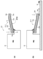
- FIG. 1 is a cross-sectional view showing the configuration and mounting form of the optical module of the present disclosure.
- FIG. 1(a) shows a schematic configuration of the optical module 100 of the present disclosure in a side cross-sectional view (x-z plane), and may be an HB-CDM optical module as an example.
- the optical module 100 includes a package 20 in which optical components and electrical components are mounted, and an FPC 10-1.
- FIG. 1(a) shows the optical module 100 in a state in which the FPC 10-1 is mounted on the package 20.
- the optical module also includes an optical fiber interface mechanism for inputting and outputting optical signals, but the optical module 100 of the present disclosure has a characteristic configuration in the connection part of the electrical signal, which is omitted in FIG. 1.
- FIG. 1(a) shows a schematic configuration of the optical module 100 of the present disclosure in a side cross-sectional view (x-z plane), and may be an HB-CDM optical module as an example.
- the optical module 100 includes a package 20 in
- FIG. 1(b) shows a side view of the optical module 100 of FIG. 1(a) mounted on a PCB 30 after being inverted 180° about the z axis on the drawing. Details of this mounting form will be described later. Please note that in each diagram in Figure 1, the relative sizes and shapes of the package 20 and FPC 10-1 are not depicted precisely, but are depicted diagrammatically.
- the optical module 100 shown in FIG. 1 is not limited to HB-CDM, but may be an HB-ICR or other optical module that inputs or outputs high-frequency electrical signals between the outside of the optical module and the outside via FPC 10-1.
- a driver IC In the case of HB-CDM, a driver IC, an optical modulator chip, a Peltier element, optical components, etc. are mounted inside the package 20.
- the Peltier element is required in the case of an InP modulator that requires a temperature adjustment mechanism. If the optical modulator element in the package is an LN modulator or a Si photonics modulator, the Peltier element is not required.
- the package 20 of the optical module 100 may be made of, for example, metal and ceramic.
- the package may be made of a material other than metal and ceramic.
- the Peltier element is generally located on the side of the package farther from the PCB 30 in FIG. 1B (the upper side of FIG. 1B), and is configured to dissipate heat from the top. It is possible to mount the Peltier element on the side closer to the PCB 30 and use a bottom-side heat dissipation configuration, but this is not a desirable configuration from the standpoint of compatibility with other components and ease of heat dissipation.
- the FPC 10-1 shown in FIG. 1(a) shows a cross section taken along the signal line of the FPC. Because it is not possible to show the structure of the FPC on an actual scale, the FPC 10-1 is shown significantly enlarged in the thickness direction.
- the FPC 10-1 is composed of a base material 11 with a thickness of 100 ⁇ m or less, and a signal line 12a and a ground (GND) layer 12b made of metal formed on the top and bottom surfaces of the base material 11.
- GND ground
- the solder resist is omitted in FIG. 1.
- the detailed structure of the top and bottom surfaces of the FPC will be described later with reference to FIG. 4 and FIG. 5.
- the FPC will be described as having two metal layers, including a layer containing the signal line 12a and a GND layer 12b, above and below the base material 11, but it may also have three or more metal layers.
- the width of the signal line 12a can be secured, and high frequency propagation loss can be reduced.
- the thickness of the base material 11 is 100 ⁇ m and 50 ⁇ m, although this depends on the characteristics of the base material 11, a signal line width of several tens of ⁇ m can be secured, so 100 ⁇ m is more suitable for broadband.
- FPC 10-1 is mounted on PCB 30 not in a flat state, but in a state curved to a certain degree.
- a thin base material with a thickness of about 50 ⁇ m is desirable.
- the thickness of base material 11 must be determined while considering whether to prioritize high-frequency transmission characteristics or bendability.
- a thickness of about 50 ⁇ m is desirable for base material 11, considering both bendability and high-frequency characteristics.
- the FPC 10-1 appears to be preformed into the shape shown in FIG. 1(a), it does not necessarily have to be formed in the state of the optical module connected to the package 20.
- the FPC 10-1 may be in an unformed flat state until mounting on the package 20 is complete, and then post-formed after mounting on the package 20. Next, a method for mounting the FPC 10-1 on the package 20 will be described.
- the FPC 10-1 is solder mounted onto an electrode pad for connection on, for example, a terrace-shaped portion of the package. Although it is possible to connect using a conductive adhesive other than solder, the wiring electrodes of the FPC are very fine patterns, and the risk of short circuits must be taken into consideration. In the optical module disclosed herein, connection using solder is optimal, as it can be protected with resist and is limited to spreading onto the metal surface.
- PADs include a connection PAD used to connect to another opposing PAD by soldering, and a heating PAD used for heating.
- a hot bar (not shown) or the like is used from above the terrace to heat and pressurize the heating PAD 13a at the top of the FPC drawing, and solder mounting is performed with the connection PAD 21 of the package 20.
- the thickness of the solder 22 between PAD 13b and PAD 21 is as thin as possible from the viewpoint of impedance matching.
- the thickness of the solder 22 needs to be 50 ⁇ m or less. If the solder 22 between the PADs is made thicker than this, the connection part including the solder 22 will have a low impedance, leading to deterioration of the high-frequency transmission characteristics. On the other hand, generally speaking, when considering the strength and long-term reliability of the solder connection, it is not desirable to give excessive priority to high-frequency characteristics and simply thin the solder 22 to 10 ⁇ m or less. Furthermore, if the FPC 10-1 and the package 20 are fixed only by solder connection, there is a risk that the solder layer will crack if an unexpected force is applied when bending and straightening the FPC, such as when mounting the package on the PCB.
- the optical module 100 adopts a configuration in which the connection between the package and the FPC is reinforced with adhesive 17 so that the solder thickness can be further reduced to 50 ⁇ m or less while ensuring the connection strength of the FPC 10-1, taking into consideration both impedance matching and connection strength.
- the adhesive 17 is applied between the end of the surface on the GND layer 12b side of the FPC 10-1 and the side surface adjacent to the terrace of the package 20. Since the adhesive 17 is a dielectric, it has a certain dielectric constant and dielectric tangent. If the adhesive 17 is applied to the surface side of the signal line 12a of the FPC 10-1, it will change the characteristic impedance of the signal line 12a and deteriorate the high-frequency transmission characteristics.
- the impact on the high-frequency transmission characteristics is suppressed by using an adhesive to fix the GND surface side of the FPC 10-1 and the side surface of the package 20.
- the impact of the adhesive is minimized by using a resin with a low dielectric constant for the adhesive 17 and limiting the application location.
- a metal signal line 12a is formed on the top surface of the base material 11 of the FPC, and a GND layer 12b for the signal line 12a is formed on the bottom surface of the base material 11. If the signal line and GND layer are configured upside down, the adhesive 17 will adhere directly to the signal line side, which may degrade the high-frequency transmission characteristics as described above. Also, in a configuration in which adhesive is used to fix the periphery of the connection between the FPC and the package, such as on the heating pad 13a or in the gap between the connection and the side of the package, rather than at the location of adhesive 17 shown in FIG. 1(a), the impedance will be further reduced by the adhesive.
- FIG. 1 shows a configuration in which the optical module 100 of (a) of FIG. 1 is mounted on a PCB 30.
- the signal line 12a may approach the metal pattern, which may degrade the high-frequency transmission characteristics.
- the electrical signal propagating through the signal line 12a is also affected by the dielectric constant of the PCB material, which also changes the characteristic impedance.
- the optical module of the present disclosure may have a different configuration.
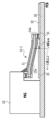
- FIG. 2 is a cross-sectional view showing another configuration and mounting form of the optical module of the present disclosure.
- FIG. 2(a) shows a schematic configuration of the optical module 101 of the present disclosure in a side cross-sectional view, which may be an HB-CDM optical module as an example.
- FIG. 2(a) shows the state after the FPC 10-2 is mounted on the package 20.
- FIG. 2(b) shows a side view of the optical module 101 of FIG. 2(a) in a state where it is inverted upside down on the drawing and mounted on the PCB 30.
- the difference from the optical module 100 of FIG. 1 is that the component surfaces of the signal line 12a and the GND layer 12b of the FPC 10-2 are upside down compared to the FPC 10-1 of FIG. 1.
- the signal line 12a is on the lower surface side of the base material 11
- the GND layer 12b is on the upper surface side of the base material 11.
- the signal line 12a of the FPC is located on the opposite side of the PCB 30, so there is no degradation of the high-frequency characteristics due to the proximity of the metal pattern of the PCB 30 and the FPC.
- the dielectric constant of the adhesive at 1 kHz must be 7.0 or less and the dielectric dissipation factor must be 0.15 or less in order to suppress the influence of the adhesive's dielectric.
- the smaller the values of the dielectric constant and dielectric dissipation factor of the adhesive the more desirable it is.
- the allowable size of adhesive applied to the signal line 12a is 800 ⁇ m or less in the signal transmission direction (x direction) along the signal line 12a.
- This allowable length in the signal transmission direction is the same as the maximum length of the connection PAD 13a on the signal line 12a side, which will be described later, and is 1/4 or less of the wavelength within the transmission line of the electrical signal propagating through the signal line.
- the wavelength within the transmission line is a wavelength that takes into account the effective dielectric constant of each material in the transmission line, etc.
- the length of the adhesive 17 in the direction along the signal line is shortened to about 100 ⁇ m, sufficient adhesive strength cannot be ensured, so a length of at least 300 ⁇ m is necessary.
- an adhesive length of 300 ⁇ m or more is also required in the height direction (z direction) along the side of the package 20 to which the adhesive 17 is applied.
- the application of the adhesive may change the high-frequency characteristics of the signal line 12a. In order to ensure connection strength and achieve a wide bandwidth for the optical module, it is desirable to meet the size of the adhesive applied to the connection portion described above.
- the adhesive 17 be fixed at a curing temperature of at least 85°C or less. This is because the FPC is mounted in the package 20 with elements and the like mounted inside, and excessively high heating may damage the internal elements and the like. 85°C is within the range generally required as an operating temperature for optical communication modules, so there is no risk of destroying the optical module. If the curing temperature is set to 85°C or higher, there is a possibility that it may have an adverse effect on the internal elements, fiber, optical connectors, and the like. However, this adverse effect can occur because it is difficult to locally heat and fix only the adhesive part, and it is assumed that the adhesive part will be heated all at once in an oven or the like. If the adhesive 17 can be fixed by local heating, it is possible to set the temperature at 85°C or higher.
- the PAD 13a of the signal line 12a and the PAD 13b of the GND layer are thermally connected to the upper and lower metals by the embedded vias or through-holes 15.
- the metals of the PADs on the upper and lower surfaces are integrated by the vias or through-holes 15, so that the heat from the metal of the heating PAD 13a on the upper surface with a hot bar can also supply heat to the solder on the connection surface side of the connection PAD 13b on the lower surface.
- embedded vias or through-holes are required along the propagation direction of the electrical signal.
- the embedded vias or through-holes for conducting between the GNDs on both sides must be arranged in at least one row along the transmission line at a pitch of 1/4 or less of the wavelength in the transmission line of the electrical signal propagating through the signal line.
- the vias or through-holes are omitted in FIG. 1.
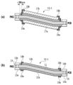
- FIG. 4 is a diagram showing the configuration of the upper and lower surfaces of the FPC of the optical module of the present disclosure.
- FIG. 4(a) is the same as the side cross-sectional view (x-z plane) of the optical module 100 of FIG. 1(b), and only the coordinate axes are newly shown.
- FIG. 4(b) is a diagram showing the upper surface (x-y plane) of the FPC 10-1 in FIG. 4(a), showing the pattern on the GDN surface side of the FPC 10-1.
- FIG. 4(c) is a diagram showing the lower surface (x-y plane) of the FPC 10-1 in FIG. 4(a), showing the pattern on the signal line side of the FPC 10-1.
- the solder resist is omitted as in FIG.
- FIG. 4(c) shows two pairs of signal lines 46-1, 46-2 in a differential signal format, and the two pairs can be, for example, the I channel and Q channel of one polarization.
- One pair of signal lines may be an I+ signal line 41-1 and an I- signal line 41-2 in the I channel of one polarization.
- the GND surface 42 in FIG. 4(b) is connected on both sides by multiple embedded vias or through-holes 44 in the direction along the signal line.
- the GND layer of the GND surface is electrically connected to the GND surface 43 of the layer containing the signal line by embedded vias or through-holes spaced at intervals of 1/4 or less of the wavelength within the transmission path of the electrical signal propagating through the signal line.
- Figs. 1 and 4 only one heating via or through hole 15 is shown for PADs 13b and 13a of FPC 10-1, but the number can be increased to two or three in the x-axis direction depending on the PAD size and the amount of heat required for solder connection.
- half through holes are provided at the longitudinal ends of the FPC to strengthen the connection strength. Since the heating of the solder is performed by the above-mentioned heating via or through hole 15, the half through holes in PADs 13a and 13b can be omitted to suppress low impedance.
- connection pads refers to PAD 13b, which is soldered to PAD 21 of package 20, and PAD 14a, which is soldered to PAD 31 of PCB 30.
- a rectangular pad overlaps with a circular land containing a via or through hole, and the diameter of the land extends beyond the rectangular area.
- the size of the connection pads described below refers to the size of the rectangular area, and it should be noted that the circular land portion outside the rectangular area is not included in the "connection pads.” As will be described later with reference to Figure 5, the circular land portion outside the rectangular area will be covered with solder resist.
- the length of the connection PADs 13b and 14a of the FPC 10-1 in the signal propagation direction (x-axis direction), which is the longitudinal direction, and the width in the short direction (y-axis direction) are both as small as possible.
- the width of the connection PAD (y-axis direction) taking into consideration the positional deviation tolerance of the FPC and the package, etc., the width of the PAD is preferably in the range of 50 ⁇ m or more and 200 ⁇ m or less. A width of 200 ⁇ m is a size that can be manufactured with sufficient stability, even considering the tolerance during mounting.
- the width of the PADs 13b and 14a is narrowed to 50 ⁇ m or less, taking into consideration the positional deviation tolerance during mounting of the FPC, the PAD 21 of the package and the connection PAD 13b of the FPC may be misaligned and may not be electrically connected, resulting in a decrease in manufacturing yield.
- the length of the connection pad of the FPC 10-1 if one or more vias or through holes 15 with a diameter of about 100 to 150 ⁇ m are placed in the pad for heating during solder connection, the length of the pad must be at least 200 ⁇ m.
- the length of the pad referred to here is the length in the x-axis direction of a rectangular area starting from the end of the FPC.
- the length of the connection pad is 800 ⁇ m or more, the capacitance added in parallel to the signal line due to the pad increases, resulting in low impedance. Therefore, from the viewpoint of widening the bandwidth of the optical module, it is desirable to set the length of the connection pad to 800 ⁇ m or less.
- connection between the FPC and the package is only by solder connection, it is not acceptable to reduce the length or width of the connection pad because it leads to a decrease in connection strength.
- connection strength can be guaranteed by fixing with the adhesive 17. It is possible to reduce the size of the connection pad that connects the package and the FPC and achieve widening the bandwidth.
- buried vias are more desirable in terms of impedance matching.
- the inside is already filled with metal, so the solder 17 between PAD 13b and PAD 21 of the package does not spill over onto PAD 13a on the top surface.
- the solder on PAD 21 of the package flows to fill the through-hole, and the solder spills over onto PAD 13a on the heated surface side.
- the thickness of PAD 13a increases equivalently, resulting in a low impedance signal line.
- the size of the through-hole or via 15 formed in the PAD must take into consideration the connection process between the FPC and the package.
- solder When a through-hole is formed in the PAD, solder must flow inside the through-hole, so it is desirable for the diameter to be 100 ⁇ m or more. Also, taking into consideration that capacitive impedance is added to the signal line, it is important to keep the diameter to 150 ⁇ m or less.
- capacitive impedance is added to the signal line, it is important to keep the diameter to 150 ⁇ m or less.
- an embedded via is formed in the PAD, there is no need to consider the flow of solder, so it is possible to reduce the size to a diameter of 150 ⁇ m or less.
- the optical module 100 in which the FPC 10-1 having the above-mentioned configuration is mounted on the package 20 is flipped 180 degrees upside down and the FPC is mounted on the PCB 30.
- the connection PAD 14a of the FPC 10-1 of the inverted optical module 100 is soldered to PAD 31 of the PCB.
- the connection between the two PADs 14a and 31 is achieved by heating and pressurizing the heating PAD 14b of the FPC 10-1 and using solder 32 via the through-hole or via 16.
- the configuration of the PADs 14a and 14b of the FPC that connect to the PAD 31 of the PCB 30 is the same as the PADs 13a and 13b that connect to the PAD 21 of the package 20 described above.
- the ceramic packaging material has a higher dielectric constant than the base material of the FPC, so there is a risk that additional capacitive impedance will be added when the FPC is connected to the package.
- the width of the PAD21 on the package side narrower than that on the FPC side. In this case, taking into account positional misalignment accuracy, etc., it is acceptable to set the width of the FPC connection pad13b wider than the PAD on the package side rather than making it the same width as the PAD21 on the package side to ensure mountability.
- the length of the connection pad in the direction along the signal line if the lengths of PAD21 of the package and PAD13a of the FPC are different, the non-overlapping portion of the longer PAD may become an open stub, which may lead to degradation of high-frequency transmission characteristics. Also, if the length of the connection pad is excessively long, there is a risk that capacitive impedance will be added to the signal line, resulting in a low impedance transmission line. For this reason, it is desirable for the lengths of PAD21 of the package and PAD13b of the FPC to be as similar as possible.
- the heating pad 13a is used for the purpose of applying heat and does not affect the mountability of the FPC 10-1, so making it narrower than the connection pad is effective in terms of reducing capacitance.
- Figure 3 shows the cross-sectional shape of an FPC including solder resist. It shows a configuration including the coverlay of Figure 3(b), which is the same as FPC 10-1 shown in Figure 1.
- a dielectric such as a coverlay
- the solder resist is omitted in Figure 1 for simplification, the solder resists 18a and 18b shown in Figure 3(a) are essential to reduce the risk of short circuits during solder mounting.
- solder resists 18a and 18b In order to reduce the risk of solder short circuits, a configuration in which the entire surface of the signal lines and GND are covered with resist can be considered, but from the perspective of high-frequency loss, it is preferable to form the solder resists 18a and 18b in a narrower area.
- FIG. 3 shows the cross-sectional configuration of FPC 10-1 including a coverlay.
- coverlays 17a and 17b By providing coverlays 17a and 17b, the signal line 12a is not exposed, so the signal line is protected and the risk of disconnection can be reduced.
- the signal line 12a is covered by coverlay 17a, which is a dielectric different from the base material 11, not air, as in (b) of FIG. 3.
- coverlay 17a which is a dielectric different from the base material 11, not air
- solder resists 18a and 18b When using a coverlay, it is desirable to place solder resists 18a and 18b so as to protect the gap between coverlay 17b and metal GND layer 12b and cover the ends of the coverlay. This makes it possible to prevent solder from flowing into the interface between the coverlay and the metal, and to prevent the adhesive layer that bonds the coverlay to the FPC surface from melting due to heat.
- gaps 47 in the GND area 42 on the GND surface of each channel. Vias or through holes 42 are densely arranged in the GND area 42. If the gaps 47 are not formed, when a thick base material is used and an FPC with a large number of signal lines and a wide width is produced, problems such as the FPC 10-1 being hard and difficult to bend may occur. By providing multiple gaps 47 along and beside the pairs of signal lines, it is possible to improve the flexibility of the FPC. It is desirable for the gaps 47 to be at least 1/3 of the total length of the FPC 10-1 in the longitudinal direction (x direction). It is also desirable for the gaps 47 to have a width of at least 100 ⁇ m in the width direction (y direction) of the FPC 10-1, taking into account processing accuracy.
- a gap 49 is required between the connecting PAD 13b and the adjacent GND region 42 (x-axis direction) for electrical isolation.
- the gap 49 is viewed from the side of the signal lines 41-1 and 41-2 in FIG. 4C, which are located behind the gap 49, there is a portion where there is no GND on the underside. Since the GND disappears in the middle of the high-frequency signal line, a discontinuity in the characteristic impedance occurs, which causes deterioration of the high-frequency transmission characteristics.
- the gap 49 between the connecting PAD 13b and the GND region 42 needs to be 200 ⁇ m or less in order to achieve a frequency band of about 100 GHz, for example.
- the higher the operating frequency the greater the effect of impedance mismatch caused by the gap 49, so it needs to be narrower.
- the gap between the above-mentioned PAD and GND should be 50 ⁇ m or more. If the connection pad 13b and the GND region 42 are too close, there is a risk of a short circuit during solder mounting due to resist tolerances, etc. Therefore, it is preferable that the gap 49 between the connection pad 13b and the GND region 42 be in the range of 50 ⁇ m or more and 200 ⁇ m or less.
- a half through hole 45 is formed at the end of the FPC 10-1 that contacts the pad.
- the half through hole 45 allows a solder fillet to be formed well when connecting to the package, and increases the solder strength.
- the connection strength of the adhesive can be sufficiently ensured, it is possible to omit the half through hole 45.
- the heating pads 13a and 14b have a narrower pad width of the rectangular portion than the connection pads 13b and 14b, as shown in (b) and (c) of FIG. 4.
- the heating pads 13a and 14b are used for heating, and may be as narrow as possible for heating, and there is no problem even if the pad width is zero (only circular lands, no rectangular area).
- the optical module disclosed herein is an optical module 100 including a flexible printed circuit (FPC) 100-1 having multiple pairs of differential signal lines, connection pads on both ends of each signal line 12a, and a package 20 having a connection pad 21 solder-joined to the connection pad 13b at one end of the signal line, and having optical elements and electrical elements mounted therein, and the FPC includes a base material 11 having a thickness of 100 ⁇ m or less, a layer including the signal lines 12a, and a ground layer (GND layer) 12b.
- FPC flexible printed circuit
- the optical module is formed from at least two or more metal layers, including the signal line, the gap 49 between the connection PAD 13b and the adjacent GND surface 42 in the direction along the signal line is 200 ⁇ m or less, the width of the connection PAD 21 of the package is narrower than the width of the connection PAD 13b of the FPC, and the GND layer is electrically connected to the GND surface of the layer including the signal line by embedded vias or through-holes 44 at intervals of 1/4 or less of the wavelength in the transmission path of the electrical signal.
- FIG. 5 shows the top and bottom surfaces of the FPC, including the solder resist.
- (a), (b), and (c) of FIG. 5 correspond to (a), (b), and (c) of FIG. 4, respectively.
- (b) of FIG. 5 shows solder resist 18a on the top side (GND side)
- (b) of FIG. 5 shows solder resist 18b on the bottom side (signal line side). It is effective to place solder resists 18a and 18b between signal lines or between signal lines and GND to prevent solder shorts, but solder resist is not essential in the optical module disclosed herein.
- FIG. 6 shows a cross-sectional configuration of the optical module of the present disclosure mounted on a PCB.
- the optical module 100 shown in FIG. 1, to which the FPC 10-1 is connected, is mounted on a PCB 30.
- the signal line 12a faces the PCB side. Therefore, if the GND surface 33 on the PCB 30 side and the signal line 12a of the FPC 10-1 are brought too close to each other, it may cause a short circuit or cause deterioration of high frequency characteristics.
- the distance between the signal line 12a of the FPC 10-1 and the GND surface 33 of the PCB 30 must be greater than the thickness of the base material 11 of the FPC. If they are closer than the thickness of the base material, the GND surface of the PCB will be closer than the GND layer 12b on the back side of the signal line 12a of the FPC, which will affect the characteristic impedance.
- the FPC 10-1 also comes close to the PCB 30 near the connection between the PAD 14a of the FPC 10-1 and the PAD 31 of the PCB. For this reason, as shown in FIG. 6, it is necessary to remove the GND surface in the part of the PCB 30 directly below the FPC 10-1. It is effective to remove the GND on the PCB 30 by at least 500 ⁇ m in the direction along the signal lines of the FPC 10-1. It is most desirable that there be no PCB GND at all below the FPC 10-1. In the mounting configuration of FIG. 6, the signal lines of the FPC are installed on the PCB surface side, and there are no signal lines on the top surface of the FPC, which is completely open to air, so it is less susceptible to the effects of radiation fields flying through space and crosstalk between channels.
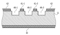
- Figure 7 is a cross-sectional view showing an impedance adjustment groove provided on the surface of the signal line of an FPC.
- Figure 7 shows a groove on the FPC side as an example, and shows a schematic cross section (y-z surface in Figure 4) of a pair of signal lines 41-1 and 41-2 in a differential signal format in the top view of FPC 10-1 shown in Figure 4(c).
- the base material 11 is engraved to form, for example, a groove 48-2 between the PAD of a signal line and the PAD between another adjacent signal line, and grooves 48-1 and 48-3 between the GND surface 43 and the PAD of the signal line.
- a groove 48-2 between the PAD of a signal line and the PAD between another adjacent signal line
- grooves 48-1 and 48-3 between the GND surface 43 and the PAD of the signal line.
- a pair of differential signal lines where the signal line is indicated as S and the ground as G, is configured as GSSG as shown in FIG. 6.
- a GND region may be further provided between the two signal lines in FIG. 6, so that it is configured as GSGSG.
- the low RF loss FPC of the optical module disclosed herein and the joint configuration between the FPC and the package improve the high frequency characteristics of the optical module and achieve a wider bandwidth.
- This invention can be used in optical communications.
Landscapes
- Physics & Mathematics (AREA)
- Nonlinear Science (AREA)
- General Physics & Mathematics (AREA)
- Optics & Photonics (AREA)
- Semiconductor Lasers (AREA)
Abstract
Description
Claims (8)
- 差動形式の信号線の複数の対と、各々の信号線の両端に接続用PADを有するフレキシブル配線基板(FPC)と、
前記信号線の一端の前記接続用PADとはんだ接合される接続用PADを有し、光素子および電気素子が内部に搭載されたパッケージと
を備えた光モジュールであって、
前記FPCは、厚さが100μm以下のベース材および信号線を含む層とグランド層(GND層)を含む少なくとも2層以上の金属層から形成されており、
前記信号線に沿った方向における、前記接続用PADと隣接するGND面との間のギャップは、200μm以下であり、
前記パッケージの前記接続用PADの幅が、前記FPCの前記接続用PADの幅よりも狭く、
前記GND層は、前記信号線を含む層のGND面と、電気信号の伝送路内波長の1/4以下の間隔で埋め込みビアまたは貫通スルーホールにて導通されていることを特徴とする光モジュール。 - 前記パッケージの前記接続用PADと前記FPCの前記接続用PADは、厚さ50μm以下のはんだで接続されており、
前記FPCの前記接続用PADは、少なくとも1つ以上の直径150μm以下の埋め込みビアで加熱用PADと接続され、前記接続用PADの前記信号線に沿った長さが800μm以下、および、前記幅が200μm以下であるか、または、
前記FPCの前記接続用PADは、少なくとも1つ以上の直径150μm以下の貫通スルーホールで加熱用PADと接続され、前記接続用PADの前記信号線に沿った長さが800μm以下、および、前記幅が200μm以下であることを特徴とする請求項1に記載の光モジュール。 - 前記FPCの前記接続用PADは、前記FPCの前記GND層の側にあり、接着剤によって、前記FPCの前記GND面および前記パッケージの側面が固定されていることを特徴とする請求項2に記載の光モジュール。
- 前記FPCの前記接続用PADは、前記FPCの前記信号線がある面の側にあり、誘電率が7.0以下、かつ、誘電正接が0.15以下の接着剤によって、前記信号線に沿った方向に800μm以下の長さに渡って、前記信号線がある面および前記パッケージの側面が固定されていることを特徴とする請求項2に記載の光モジュール。
- 前記FPCの隣接する前記複数の対の間であって、前記信号線に沿った方向における前記FPCの全長の1/3以上の長さの範囲に、100μm以上の幅の空隙が設けられていることを特徴とする請求項3または4に記載の光モジュール。
- 前記接続用PADおよび前記加熱用PADの部位を除いた、前記FPCの両面上に、カバーレイフィルムが形成されており、前記カバーレイフィルムの端および前記接続用PADの周囲がソルダーレジストで覆われていることを特徴とする請求項5に記載の光モジュール。
- 前記FPCの前記ベース材および前記パッケージの前記接続用PADの形成された面の少なくともいずれか一方において、1つの対内の前記信号線の間、または、前記信号線および隣接するGND領域の間に、前記信号線に沿って溝が形成されていることを特徴とする請求項6に記載の光モジュール。
- 前記光モジュールは、プリント回路基板(PCB)に搭載され、
前記信号線の他端の前記接続用PADと前記PCBの接続用PADとが、はんだ接続され、
前記PCBの前記接続用PADは、前記PCBのGND領域から500μm以上離れており、
前記FPCの前記信号線を含む面は、前記FPCの厚さ方向について、前記PCBの前記GND領域から前記ベース材の厚さ以上離れていることを特徴とする請求項3に記載の光モジュール。
Priority Applications (2)
| Application Number | Priority Date | Filing Date | Title |
|---|---|---|---|
| PCT/JP2023/006834 WO2024176458A1 (ja) | 2023-02-24 | 2023-02-24 | 光モジュール |
| JP2025502075A JPWO2024176458A1 (ja) | 2023-02-24 | 2023-02-24 |
Applications Claiming Priority (1)
| Application Number | Priority Date | Filing Date | Title |
|---|---|---|---|
| PCT/JP2023/006834 WO2024176458A1 (ja) | 2023-02-24 | 2023-02-24 | 光モジュール |
Publications (1)
| Publication Number | Publication Date |
|---|---|
| WO2024176458A1 true WO2024176458A1 (ja) | 2024-08-29 |
Family
ID=92500509
Family Applications (1)
| Application Number | Title | Priority Date | Filing Date |
|---|---|---|---|
| PCT/JP2023/006834 Ceased WO2024176458A1 (ja) | 2023-02-24 | 2023-02-24 | 光モジュール |
Country Status (2)
| Country | Link |
|---|---|
| JP (1) | JPWO2024176458A1 (ja) |
| WO (1) | WO2024176458A1 (ja) |
Citations (9)
| Publication number | Priority date | Publication date | Assignee | Title |
|---|---|---|---|---|
| JP2003133814A (ja) * | 2001-10-24 | 2003-05-09 | Kyocera Corp | 高周波用配線基板 |
| JP2003224408A (ja) * | 2002-01-30 | 2003-08-08 | Kyocera Corp | 高周波用配線基板 |
| JP2011095333A (ja) * | 2009-10-27 | 2011-05-12 | Toshiba Corp | 実装構造体 |
| JP2016194600A (ja) * | 2015-03-31 | 2016-11-17 | 住友大阪セメント株式会社 | 光変調器モジュール |
| JP2017072813A (ja) * | 2015-10-09 | 2017-04-13 | 富士通オプティカルコンポーネンツ株式会社 | 光モジュール及び光伝送装置 |
| US20180082929A1 (en) * | 2017-08-01 | 2018-03-22 | Xiamen Tianma Micro-Electronics Co., Ltd. | Display panel and display device |
| WO2019050046A1 (ja) * | 2017-09-11 | 2019-03-14 | Ngkエレクトロデバイス株式会社 | 配線基板とフレキシブル基板の接続構造および電子部品収納用パッケージ |
| JP2020020876A (ja) * | 2018-07-30 | 2020-02-06 | 住友大阪セメント株式会社 | 光変調器および光送信装置 |
| WO2020049723A1 (ja) * | 2018-09-07 | 2020-03-12 | 三菱電機株式会社 | 光モジュール |
-
2023
- 2023-02-24 JP JP2025502075A patent/JPWO2024176458A1/ja active Pending
- 2023-02-24 WO PCT/JP2023/006834 patent/WO2024176458A1/ja not_active Ceased
Patent Citations (9)
| Publication number | Priority date | Publication date | Assignee | Title |
|---|---|---|---|---|
| JP2003133814A (ja) * | 2001-10-24 | 2003-05-09 | Kyocera Corp | 高周波用配線基板 |
| JP2003224408A (ja) * | 2002-01-30 | 2003-08-08 | Kyocera Corp | 高周波用配線基板 |
| JP2011095333A (ja) * | 2009-10-27 | 2011-05-12 | Toshiba Corp | 実装構造体 |
| JP2016194600A (ja) * | 2015-03-31 | 2016-11-17 | 住友大阪セメント株式会社 | 光変調器モジュール |
| JP2017072813A (ja) * | 2015-10-09 | 2017-04-13 | 富士通オプティカルコンポーネンツ株式会社 | 光モジュール及び光伝送装置 |
| US20180082929A1 (en) * | 2017-08-01 | 2018-03-22 | Xiamen Tianma Micro-Electronics Co., Ltd. | Display panel and display device |
| WO2019050046A1 (ja) * | 2017-09-11 | 2019-03-14 | Ngkエレクトロデバイス株式会社 | 配線基板とフレキシブル基板の接続構造および電子部品収納用パッケージ |
| JP2020020876A (ja) * | 2018-07-30 | 2020-02-06 | 住友大阪セメント株式会社 | 光変調器および光送信装置 |
| WO2020049723A1 (ja) * | 2018-09-07 | 2020-03-12 | 三菱電機株式会社 | 光モジュール |
Also Published As
| Publication number | Publication date |
|---|---|
| JPWO2024176458A1 (ja) | 2024-08-29 |
Similar Documents
| Publication | Publication Date | Title |
|---|---|---|
| US6879032B2 (en) | Folded flex circuit interconnect having a grid array interface | |
| US9244230B2 (en) | Optical transmitter and interconnecting circuit board | |
| JP5310239B2 (ja) | 接続端子および伝送線路 | |
| CN104220909B9 (zh) | 使用介电波导的芯片间通信 | |
| CN101971414B (zh) | 连接装置以及光器件 | |
| US8044746B2 (en) | Flexible interconnect cable with first and second signal traces disposed between first and second ground traces so as to provide different line width and line spacing configurations | |
| JP5580994B2 (ja) | 光モジュール | |
| US10231327B1 (en) | Optical module and optical transmission equipment | |
| CN104914517B (zh) | 光模块 | |
| US10042133B2 (en) | Optical module | |
| CN107656384B (zh) | 带有fpc的光调制器及使用该光调制器的光发送装置 | |
| JP5609451B2 (ja) | コネクタ、光伝送装置およびコネクタ接続方法 | |
| CN111679457B (zh) | 光调制器及使用了该光调制器的光发送装置 | |
| US8585432B2 (en) | Connector and optical transmission apparatus | |
| JP6128859B2 (ja) | 光モジュール | |
| US11744008B2 (en) | Printed board and printed board assembly | |
| JP2004093606A (ja) | 光モジュール及び光伝送装置 | |
| WO2010061582A1 (ja) | 回路モジュールの基板及びその製造方法 | |
| JP7769265B2 (ja) | 光モジュール | |
| EP4738729A1 (en) | Optical transceiver, and method and apparatus for manufacturing same | |
| WO2017163459A1 (ja) | Fpc付き光変調器、及びそれを用いた光送信装置 | |
| EP4723515A1 (en) | Optical transceiver | |
| JP7187871B2 (ja) | 光変調器および光送信装置 | |
| WO2025004226A1 (ja) | 光トランシーバ | |
| CA3296177A1 (en) | Optical transceiver, and manufacturing method, and manufacturing equipment thereof |
Legal Events
| Date | Code | Title | Description |
|---|---|---|---|
| 121 | Ep: the epo has been informed by wipo that ep was designated in this application |
Ref document number: 23924106 Country of ref document: EP Kind code of ref document: A1 |
|
| ENP | Entry into the national phase |
Ref document number: 2025502075 Country of ref document: JP Kind code of ref document: A |
|
| WWE | Wipo information: entry into national phase |
Ref document number: 2025502075 Country of ref document: JP |
|
| NENP | Non-entry into the national phase |
Ref country code: DE |
|
| 122 | Ep: pct application non-entry in european phase |
Ref document number: 23924106 Country of ref document: EP Kind code of ref document: A1 |