WO2024171659A1 - 多層基板、電子機器及び多層基板の製造方法 - Google Patents
多層基板、電子機器及び多層基板の製造方法 Download PDFInfo
- Publication number
- WO2024171659A1 WO2024171659A1 PCT/JP2024/000392 JP2024000392W WO2024171659A1 WO 2024171659 A1 WO2024171659 A1 WO 2024171659A1 JP 2024000392 W JP2024000392 W JP 2024000392W WO 2024171659 A1 WO2024171659 A1 WO 2024171659A1
- Authority
- WO
- WIPO (PCT)
- Prior art keywords
- axis
- hole
- layer
- interlayer connection
- insulator layer
- Prior art date
- Legal status (The legal status is an assumption and is not a legal conclusion. Google has not performed a legal analysis and makes no representation as to the accuracy of the status listed.)
- Ceased
Links
Images


Classifications
-
- H—ELECTRICITY
- H05—ELECTRIC TECHNIQUES NOT OTHERWISE PROVIDED FOR
- H05K—PRINTED CIRCUITS; CASINGS OR CONSTRUCTIONAL DETAILS OF ELECTRIC APPARATUS; MANUFACTURE OF ASSEMBLAGES OF ELECTRICAL COMPONENTS
- H05K3/00—Apparatus or processes for manufacturing printed circuits
- H05K3/46—Manufacturing multilayer circuits
- H05K3/4611—Manufacturing multilayer circuits by laminating two or more circuit boards
- H05K3/4614—Manufacturing multilayer circuits by laminating two or more circuit boards the electrical connections between the circuit boards being made during lamination
- H05K3/4617—Manufacturing multilayer circuits by laminating two or more circuit boards the electrical connections between the circuit boards being made during lamination characterized by laminating only or mainly similar single-sided circuit boards
-
- H—ELECTRICITY
- H01—ELECTRIC ELEMENTS
- H01P—WAVEGUIDES; RESONATORS, LINES, OR OTHER DEVICES OF THE WAVEGUIDE TYPE
- H01P3/00—Waveguides; Transmission lines of the waveguide type
- H01P3/12—Hollow waveguides
-
- H—ELECTRICITY
- H05—ELECTRIC TECHNIQUES NOT OTHERWISE PROVIDED FOR
- H05K—PRINTED CIRCUITS; CASINGS OR CONSTRUCTIONAL DETAILS OF ELECTRIC APPARATUS; MANUFACTURE OF ASSEMBLAGES OF ELECTRICAL COMPONENTS
- H05K1/00—Printed circuits
- H05K1/02—Details
- H05K1/0213—Electrical arrangements not otherwise provided for
- H05K1/0216—Reduction of cross-talk, noise or electromagnetic interference
- H05K1/0218—Reduction of cross-talk, noise or electromagnetic interference by printed shielding conductors, ground planes or power plane
- H05K1/0219—Printed shielding conductors for shielding around or between signal conductors, e.g. coplanar or coaxial printed shielding conductors
-
- H—ELECTRICITY
- H05—ELECTRIC TECHNIQUES NOT OTHERWISE PROVIDED FOR
- H05K—PRINTED CIRCUITS; CASINGS OR CONSTRUCTIONAL DETAILS OF ELECTRIC APPARATUS; MANUFACTURE OF ASSEMBLAGES OF ELECTRICAL COMPONENTS
- H05K1/00—Printed circuits
- H05K1/02—Details
- H05K1/0213—Electrical arrangements not otherwise provided for
- H05K1/0237—High frequency adaptations
- H05K1/024—Dielectric details, e.g. changing the dielectric material around a transmission line
-
- H—ELECTRICITY
- H05—ELECTRIC TECHNIQUES NOT OTHERWISE PROVIDED FOR
- H05K—PRINTED CIRCUITS; CASINGS OR CONSTRUCTIONAL DETAILS OF ELECTRIC APPARATUS; MANUFACTURE OF ASSEMBLAGES OF ELECTRICAL COMPONENTS
- H05K1/00—Printed circuits
- H05K1/02—Details
- H05K1/0296—Conductive pattern lay-out details not covered by sub groups H05K1/02 - H05K1/0295
- H05K1/0298—Multilayer circuits
-
- H—ELECTRICITY
- H05—ELECTRIC TECHNIQUES NOT OTHERWISE PROVIDED FOR
- H05K—PRINTED CIRCUITS; CASINGS OR CONSTRUCTIONAL DETAILS OF ELECTRIC APPARATUS; MANUFACTURE OF ASSEMBLAGES OF ELECTRICAL COMPONENTS
- H05K1/00—Printed circuits
- H05K1/02—Details
- H05K1/03—Use of materials for the substrate
-
- H—ELECTRICITY
- H05—ELECTRIC TECHNIQUES NOT OTHERWISE PROVIDED FOR
- H05K—PRINTED CIRCUITS; CASINGS OR CONSTRUCTIONAL DETAILS OF ELECTRIC APPARATUS; MANUFACTURE OF ASSEMBLAGES OF ELECTRICAL COMPONENTS
- H05K1/00—Printed circuits
- H05K1/02—Details
- H05K1/11—Printed elements for providing electric connections to or between printed circuits
- H05K1/115—Via connections; Lands around holes or via connections
- H05K1/116—Lands, clearance holes or other lay-out details concerning the surrounding of a via
-
- H—ELECTRICITY
- H05—ELECTRIC TECHNIQUES NOT OTHERWISE PROVIDED FOR
- H05K—PRINTED CIRCUITS; CASINGS OR CONSTRUCTIONAL DETAILS OF ELECTRIC APPARATUS; MANUFACTURE OF ASSEMBLAGES OF ELECTRICAL COMPONENTS
- H05K3/00—Apparatus or processes for manufacturing printed circuits
- H05K3/40—Forming printed elements for providing electric connections to or between printed circuits
- H05K3/4038—Through-connections; Vertical interconnect access [VIA] connections
-
- H—ELECTRICITY
- H05—ELECTRIC TECHNIQUES NOT OTHERWISE PROVIDED FOR
- H05K—PRINTED CIRCUITS; CASINGS OR CONSTRUCTIONAL DETAILS OF ELECTRIC APPARATUS; MANUFACTURE OF ASSEMBLAGES OF ELECTRICAL COMPONENTS
- H05K3/00—Apparatus or processes for manufacturing printed circuits
- H05K3/46—Manufacturing multilayer circuits
- H05K3/4611—Manufacturing multilayer circuits by laminating two or more circuit boards
- H05K3/4626—Manufacturing multilayer circuits by laminating two or more circuit boards characterised by the insulating layers or materials
- H05K3/4632—Manufacturing multilayer circuits by laminating two or more circuit boards characterised by the insulating layers or materials laminating thermoplastic or uncured resin sheets comprising printed circuits without added adhesive materials between the sheets
-
- H—ELECTRICITY
- H05—ELECTRIC TECHNIQUES NOT OTHERWISE PROVIDED FOR
- H05K—PRINTED CIRCUITS; CASINGS OR CONSTRUCTIONAL DETAILS OF ELECTRIC APPARATUS; MANUFACTURE OF ASSEMBLAGES OF ELECTRICAL COMPONENTS
- H05K3/00—Apparatus or processes for manufacturing printed circuits
- H05K3/46—Manufacturing multilayer circuits
- H05K3/4611—Manufacturing multilayer circuits by laminating two or more circuit boards
- H05K3/4626—Manufacturing multilayer circuits by laminating two or more circuit boards characterised by the insulating layers or materials
- H05K3/4635—Manufacturing multilayer circuits by laminating two or more circuit boards characterised by the insulating layers or materials laminating flexible circuit boards using additional insulating adhesive materials between the boards
-
- H—ELECTRICITY
- H05—ELECTRIC TECHNIQUES NOT OTHERWISE PROVIDED FOR
- H05K—PRINTED CIRCUITS; CASINGS OR CONSTRUCTIONAL DETAILS OF ELECTRIC APPARATUS; MANUFACTURE OF ASSEMBLAGES OF ELECTRICAL COMPONENTS
- H05K2201/00—Indexing scheme relating to printed circuits covered by H05K1/00
- H05K2201/01—Dielectrics
- H05K2201/0137—Materials
- H05K2201/0141—Liquid crystal polymer [LCP]
-
- H—ELECTRICITY
- H05—ELECTRIC TECHNIQUES NOT OTHERWISE PROVIDED FOR
- H05K—PRINTED CIRCUITS; CASINGS OR CONSTRUCTIONAL DETAILS OF ELECTRIC APPARATUS; MANUFACTURE OF ASSEMBLAGES OF ELECTRICAL COMPONENTS
- H05K2201/00—Indexing scheme relating to printed circuits covered by H05K1/00
- H05K2201/01—Dielectrics
- H05K2201/0137—Materials
- H05K2201/015—Fluoropolymer, e.g. polytetrafluoroethylene [PTFE]
-
- H—ELECTRICITY
- H05—ELECTRIC TECHNIQUES NOT OTHERWISE PROVIDED FOR
- H05K—PRINTED CIRCUITS; CASINGS OR CONSTRUCTIONAL DETAILS OF ELECTRIC APPARATUS; MANUFACTURE OF ASSEMBLAGES OF ELECTRICAL COMPONENTS
- H05K2201/00—Indexing scheme relating to printed circuits covered by H05K1/00
- H05K2201/01—Dielectrics
- H05K2201/0137—Materials
- H05K2201/0154—Polyimide
-
- H—ELECTRICITY
- H05—ELECTRIC TECHNIQUES NOT OTHERWISE PROVIDED FOR
- H05K—PRINTED CIRCUITS; CASINGS OR CONSTRUCTIONAL DETAILS OF ELECTRIC APPARATUS; MANUFACTURE OF ASSEMBLAGES OF ELECTRICAL COMPONENTS
- H05K2201/00—Indexing scheme relating to printed circuits covered by H05K1/00
- H05K2201/09—Shape and layout
- H05K2201/09818—Shape or layout details not covered by a single group of H05K2201/09009 - H05K2201/09809
- H05K2201/09827—Tapered, e.g. tapered hole, via or groove
Definitions
- the present invention relates to a multilayer substrate having a structure in which multiple insulating layers are stacked.
- a known example of a conventional invention related to a multilayer board is the signal transmission line described in Patent Document 1.
- This signal transmission line includes an interlayer connection conductor.
- the object of the present invention is to provide a multilayer board, an electronic device, and a method for manufacturing a multilayer board that can suppress damage to interlayer connection conductors.
- a multilayer substrate comprises:
- the multilayer substrate includes a laminate, a first conductor layer, a second conductor layer, and a first interlayer connection conductor,
- the laminate has a structure in which a plurality of insulator layers including a first insulator layer and a second insulator layer are laminated along a Z axis, Each of the first and second insulator layers has a positive and a negative principal surface, a positive principal surface of the second insulator layer in contact with a negative principal surface of the first insulator layer;
- the first conductor layer is located on the positive side of the Z-axis relative to the first insulator layer, the second conductor layer is located on the negative side of the Z axis relative to the second insulator layer,
- the first insulating layer is provided with a first through hole penetrating the first insulating layer along the Z-axis,
- the second insulating layer is provided with a second through hole penetrating the second insulating layer along the Z-axi
- a method for manufacturing a multilayer substrate includes the steps of: providing a first insulator layer and a second insulator layer having positive and negative major surfaces aligned along a Z-axis; a first through hole forming step of forming a first through hole penetrating the first insulator layer along the Z-axis; a second through hole forming step of forming a second through hole penetrating the second insulator layer along the Z-axis; a first interlayer connection conductor forming step of stacking the first insulator layer and the second insulator layer so that a negative principal surface of the first insulator layer and a positive principal surface of the second insulator layer are in contact with each other, and forming a first interlayer connection conductor extending along the Z-axis within the first through hole and the second through hole; Equipped with When viewed in a positive direction of the Z axis, an area of an end of the second through hole on the positive side of the Z axis is larger than an area
- the multilayer board and the method for manufacturing the multilayer board according to the present invention can prevent damage to the first interlayer connection conductor.
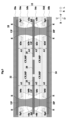
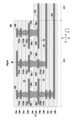
- FIG. 1 is an exploded perspective view of a multilayer substrate 10.
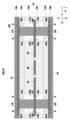
- FIG. FIG. 2 is a cross-sectional view of the multilayer substrate 10.
- FIG. 3 is a cross-sectional view of the multilayer substrate 10.
- FIG. 4 is a cross-sectional view of the multilayer substrate 10 during its manufacture.
- FIG. 5 is a cross-sectional view of the multilayer substrate 10a.
- FIG. 6 is a cross-sectional view of the multilayer substrate 10b.
- FIG. 7 is a cross-sectional view of the multilayer substrate 10c.
- FIG. 8 is a cross-sectional view of the multilayer substrate 10d.
- FIG. 9 is a cross-sectional view of the multilayer substrate 10e.
- FIG. 10 is a cross-sectional view of the multilayer substrate 10f.
- FIG. 11 is a cross-sectional view of a multilayer substrate 10g.
- FIG. 12 is a cross-sectional view of a multilayer substrate 10h.
- FIG. 13 is a cross-sectional view of the multilayer substrate 10i.
- FIG. 14 is a cross-sectional view of the multilayer substrate 10j.
- FIG. 15 is a cross-sectional view of the vicinity of the first interlayer connection conductor v3 of the multilayer substrate 10k.
- FIG. 16 is a cross-sectional view of the vicinity of the first interlayer connection conductor v3 of the multilayer substrate 10l.
- FIG. 17 is a cross-sectional view of the vicinity of the first interlayer connection conductor v3 of the multilayer substrate 10m.
- FIG. 18 is a cross-sectional view of the vicinity of the first interlayer connection conductor v3a of the multilayer substrate 10n.
- FIG. 19 is a cross-sectional view of the multilayer substrate 10o.
- FIG. 20 is a cross-sectional view of the multilayer substrate 10p.
- FIG. 21 is a cross-sectional view of an electronic device 1 including a multilayer substrate 10.
- FIG. 1 is an exploded perspective view of the multilayer substrate 10.
- Figs. 2 and 3 are cross-sectional views of the multilayer substrate 10.
- Fig. 2 shows a cross-section taken along line A-A in Fig. 1.
- Fig. 3 shows a cross-section taken along line B-B in Fig. 1. Note that in Fig. 1, reference symbols are given only to representative first interlayer connection conductors v3, v4 among the multiple first interlayer connection conductors v3, v4.
- the stacking direction of the laminate 12 of the multilayer substrate 10 is parallel to the up-down axis.
- the up-down axis coincides with the Z axis.
- the upward direction is the positive direction of the Z axis.
- the downward direction is the negative direction of the Z axis.
- the extension direction of the signal conductor layer 20 of the multilayer substrate 10 is parallel to the left-right axis.
- the line width direction of the signal conductor layer 20 when viewed from below is parallel to the front-rear axis.
- the up-down axis, front-rear axis, and left-right axis are mutually orthogonal.
- up-down axis, left-right axis, and front-rear axis do not have to coincide with the up-down axis, left-right axis, and front-rear axis when the multilayer substrate 10 is in use.
- X is a part or member of the multilayer substrate 10.
- each part of X is defined as follows:
- the front part of X means the front half of X.
- the rear part of X means the rear half of X.
- the left part of X means the left half of X.
- the right part of X means the right half of X.
- the upper part of X means the upper half of X.
- the lower part of X means the lower half of X.
- the front end of X means the front end of X.
- the rear end of X means the rear end of X.
- the left end of X means the left end of X.
- the right end of X means the right end of X.
- the upper end of X means the upper end of X.
- the lower end of X means the lower end of X.
- the front end of X means the front end of X and its vicinity.
- the rear end of X means the rear end of X and its vicinity.
- the left end of X means the left end of X and its vicinity.
- the right end of X means the right end of X and its vicinity.
- the upper end of X means the upper end of X and its vicinity.
- the lower end of X means the lower end of X and its vicinity.
- the multilayer board 10 transmits high-frequency signals.
- the multilayer board 10 is used to electrically connect two circuits in electronic devices such as smartphones.
- the multilayer board 10 includes a laminate 12, protective layers 18a and 18b, a signal conductor layer 20, a first ground conductor layer 22 (first conductor layer), a second ground conductor layer 24, a third ground conductor layer 25 (second conductor layer), mounting electrodes 26a and 26b, first interlayer connection conductors v1 and v2, a plurality of first interlayer connection conductors v3, and a plurality of first interlayer connection conductors v4.
- the laminate 12 has a plate shape.
- the laminate 12 has an upper main surface and a lower main surface located below the upper main surface.
- the upper and lower main surfaces of the laminate 12 have a rectangular shape with long sides extending along the left-right axis.
- the length of the laminate 12 on the left-right axis is longer than the length of the laminate 12 on the front-back axis.
- the laminate 12 is flexible.
- the laminate 12 has a structure in which a plurality of insulator layers 16a to 16d, including insulator layer 16a (first insulator layer) and insulator layer 16b (second insulator layer), are stacked along the vertical axis (Z-axis).
- Each of the insulator layers 16a to 16d has an upper main surface (positive main surface) and a lower main surface (negative main surface).
- the insulator layers 16a to 16d are arranged in this order from top to bottom.
- the upper main surface (positive main surface) of the insulator layer 16b (second insulator layer) is in contact with the negative main surface of the insulator layer 16a (first insulator layer).
- the lower main surface of the insulator layer 16c is in contact with the upper main surface of the insulator layer 16d.
- the material of the insulator layers 16a to 16d is, for example, a thermoplastic resin.
- the thermoplastic resin is, for example, a liquid crystal polymer.
- the material of the insulator layers 16a to 16d (the material of the first insulator layer and the material of the second insulator layer) is a flexible resin.
- the insulator layers 16a to 16d are fused together with adjacent layers vertically. That is, the insulator layer 16a (first insulator layer) and the insulator layer 16b (second insulator layer) are fused together.
- the insulator layer 16c and the insulator layer 16d are fused together.
- a high-frequency signal is transmitted to the signal conductor layer 20.
- the signal conductor layer 20 is provided in the laminate 12.
- the signal conductor layer 20 is located on the lower main surface of the insulator layer 16b.
- the signal conductor layer 20 has a linear shape extending along the left-right axis.
- the first ground conductor layer 22 is provided in the laminate 12 as shown in FIG. 1.
- the first ground conductor layer 22 is located above the signal conductor layer 20 and overlaps with the signal conductor layer 20 when viewed in the downward direction.
- the first ground conductor layer 22 is located on the upper main surface of the insulator layer 16a.
- the first ground conductor layer 22 (first conductor layer) is located above (on the positive side of the Z axis) the insulator layer 16a (first insulator layer).
- the first ground conductor layer 22 also covers substantially the entire upper main surface of the insulator layer 16a. A ground potential is connected to the first ground conductor layer 22.
- the second ground conductor layer 24 is provided in the laminate 12 as shown in FIG. 1.
- the second ground conductor layer 24 is located below the signal conductor layer 20 and overlaps with the signal conductor layer 20 when viewed in the downward direction.
- the second ground conductor layer 24 is located on the lower main surface of the insulator layer 16d.
- the second ground conductor layer 24 is located below the insulator layer 16d.
- the second ground conductor layer 24 also covers substantially the entire lower main surface of the insulator layer 16d.
- a ground potential is connected to the second ground conductor layer 24.
- the signal conductor layer 20, the first ground conductor layer 22, and the second ground conductor layer 24 as described above have a stripline structure.
- the third ground conductor layer 25 is provided in the laminate 12 as shown in FIG. 1.
- the third ground conductor layer 25 is located below the first ground conductor layer 22 and above the second ground conductor layer 24.
- the third ground conductor layer 25 is located on the lower main surface of the insulator layer 16b.
- the third ground conductor layer 25 (second conductor layer) is located below (on the negative side of the Z axis) the insulator layer 16b (second insulator layer).
- the third ground conductor layer 25 covers substantially the entire lower main surface of the insulator layer 16b.
- the third ground conductor layer 25 is not in contact with the signal conductor layer 20. Therefore, an opening is provided in the third ground conductor layer 25.
- the signal conductor layer 20 is located inside the opening.
- a ground potential is connected to the third ground conductor layer 25.
- the mounting electrode 26a is provided on the laminate 12 as shown in FIG. 1.
- the mounting electrode 26a is located on the upper main surface of the laminate 12. More specifically, the mounting electrode 26a is located at the left end of the upper main surface of the insulator layer 16a. When viewed from below, the mounting electrode 26a overlaps with the left end of the signal conductor layer 20. When viewed from below, the mounting electrode 26a has a rectangular shape.
- the mounting electrode 26a is an external terminal through which high-frequency signals are input and output.
- the mounting electrode 26a is not in contact with the first ground conductor layer 22.
- the structure of the mounting electrode 26b is symmetrical to the structure of the mounting electrode 26a, so a description thereof will be omitted.
- the first interlayer connection conductor v1 is provided in the laminate 12 as shown in FIG. 1.
- the first interlayer connection conductor v1 electrically connects the mounting electrode 26a and the left end of the signal conductor layer 20 as shown in FIG. 1 and FIG. 2.
- the insulator layer 16a (first insulator layer) is provided with a first through hole h1a that penetrates the insulator layer 16a (first insulator layer) along the up-down axis (Z-axis).
- the first through hole h1a has a tapered shape that becomes thinner as it goes upward (positive direction of the Z-axis). Therefore, the upper end of the first through hole h1a is thinner than the lower end of the first through hole h1a.
- the insulator layer 16b (second insulator layer) is provided with a plurality of second through holes h1b that penetrate the insulator layer 16b (second insulator layer) along the up-down axis (Z-axis).
- the second through holes h1b have a tapered shape that becomes thinner as it goes downward (negative/positive direction of the Z-axis). Therefore, the lower end of the second through holes h1b is thinner than the upper end of the second through holes h1b.
- the second through hole h1b overlaps with the first through hole h1a when viewed in the downward direction.
- the area of the upper end (end on the positive side of the Z axis) of the second through hole h1b is larger than the area of the lower end (end on the negative side of the Z axis) of the first through hole h1a.
- the lower end (end on the negative side of the Z axis) of the first through hole h1a is contained within the upper end (end on the positive side of the Z axis) of the second through hole h1b.
- the lower end of the first through hole h1a does not protrude from the upper end of the second through hole h1b.
- the second through hole h1b is connected to the first through hole h1a.
- the first interlayer connection conductor v1 extends along the vertical axis (Z axis) within the first through hole h1a and the second through hole h1b.
- the upper end UP of the first interlayer connection conductor v1 is in contact with the mounting electrode 26a.
- the lower end DP of the first interlayer connection conductor v1 is in contact with the left end of the signal conductor layer 20.
- the first interlayer connection conductor v1 has an intermediate portion MP located between the upper end UP (the end on the positive side of the Z axis) of the first interlayer connection conductor v1 and the lower end DP (the end on the negative side of the Z axis) of the first interlayer connection conductor v1.
- the intermediate portion MP is located at the same position as the center CP of the first interlayer connection conductor v1 on the vertical axis (Z axis). However, the intermediate portion MP does not have to coincide with the center CP.
- the first interlayer connection conductor v1 has a first section A1 that has a tapered shape that becomes thinner as it approaches the middle section MP from the upper end UP (the end on the positive side of the Z axis), and a second section A2 that has a tapered shape that becomes thinner as it approaches the middle section MP from the lower end DP (the end on the negative side of the Z axis).
- a space Sp0 exists between the boundary between the insulator layer 16a (first insulator layer) and the insulator layer 16b (second insulator layer) and the first interlayer connection conductor v1. Furthermore, the space Sp0 exists between the inner surface of the second through hole h1b and the center CP of the first interlayer connection conductor v1 in the vertical axis (Z axis).
- the space Sp0 faces at least a portion of the inner surface of the first through hole h1a and also faces at least a portion of the inner surface of the second through hole h1b. In this embodiment, the space Sp0 faces the entire inner surface of the first through hole h1a and also faces the entire inner surface of the second through hole h1b.
- the first interlayer connection conductor v1 is in contact only with the upper end of the inner circumferential surface of the first through hole h1a and the lower end of the inner circumferential surface of the second through hole h1b, and is not in contact with any part of the inner circumferential surface of the first through hole h1a other than the upper end and any part of the inner circumferential surface of the second through hole h1b other than the lower end. Therefore, due to the existence of the space Sp0, the first interlayer connection conductor v1 is not in contact with the boundary between the insulator layer 16a (first insulator layer) and the insulator layer 16b (second insulator layer).
- First interlayer connection conductor First interlayer connection conductor First interlayer connection conductor First interlayer connection conductor First interlayer connection conductor First interlayer connection conductor First interlayer connection conductor First interlayer connection conductor
- a high-frequency signal having a frequency of 1 GHz or more and 1 THz or less is transmitted to the mounting electrodes 26a, 26b (first conductor layer), the signal conductor layer 20 (second conductor layer), and the first interlayer connection conductors v1, v2 as described above.
- each of the first interlayer connection conductors v3 includes first interlayer connection conductors v3a and v3b.
- Each of the first interlayer connection conductors v3a electrically connects the first ground conductor layer 22 (first conductor layer) and the third ground conductor layer 25 (second conductor layer).
- the insulator layer 16a (first insulator layer) is provided with a plurality of first through holes h3a that penetrate the insulator layer 16a (first insulator layer) along the vertical axis (Z axis).
- Each of the first through holes h3a has a tapered shape that becomes thinner as it goes upward (positive direction of the Z axis).
- the first through holes h3a are located in front of the signal conductor layer 20 when viewed in the downward direction.
- the first through holes h3a are arranged in a row along the horizontal axis.
- the insulator layer 16b (second insulator layer) is provided with a plurality of second through holes h3b that penetrate the insulator layer 16b (second insulator layer) along the up-down axis (Z axis).
- Each of the plurality of second through holes h3b has a tapered shape that becomes thinner in the downward direction (negative-positive direction of the Z axis). Therefore, the lower end of the second through hole h3b is thinner than the upper end of the second through hole h3b.
- the plurality of second through holes h3b are located in front of the signal conductor layer 20 when viewed in the downward direction.
- the plurality of second through holes h3b are aligned in a line along the left-right axis. In other words, the plurality of second through holes h3b are aligned along the signal line.
- the second through holes h3b overlap with the first through holes h3a when viewed downward.
- the area of the upper end (end on the positive side of the Z axis) of the second through hole h3b is larger than the area of the lower end (end on the negative side of the Z axis) of the first through hole h3a.
- the lower end (end on the negative side of the Z axis) of the first through hole h3a is contained in the upper end (end on the positive side of the Z axis) of the second through hole h3b.
- the lower end of the first through hole h3a does not protrude from the upper end of the second through hole h3b.
- the second through holes h3b are connected to the first through holes h3a.
- the first interlayer connection conductor v3a extends along the vertical axis (Z axis) within the first through hole h3a and the second through hole h3b.
- the upper end UP of the first interlayer connection conductor v3a is in contact with the first ground conductor layer 22.
- the lower end DP of the first interlayer connection conductor v3a is in contact with the third ground conductor layer 25.
- the first interlayer connection conductor v3a has an intermediate portion MP located between the upper end UP (the end on the positive side of the Z axis) of the first interlayer connection conductor v3a and the lower end DP (the end on the negative side of the Z axis) of the first interlayer connection conductor v3a.
- the intermediate portion MP is located at the same position as the center CP of the first interlayer connection conductor v3a on the vertical axis (Z axis). However, the intermediate portion MP does not have to coincide with the center CP.
- the first interlayer connection conductor v3a has a first section A1 that has a tapered shape that narrows from the upper end UP (the end on the positive side of the Z axis) toward the middle section MP, and a second section A2 that has a tapered shape that narrows from the lower end DP (the end on the negative side of the Z axis) toward the middle section MP.
- a space Sp1 exists between the boundary between the insulator layer 16a (first insulator layer) and the insulator layer 16b (second insulator layer) and the first interlayer connection conductor v3a. Furthermore, the space Sp1 exists between the inner surface of the second through hole h3b and the center CP of the first interlayer connection conductor v3a in the vertical axis (Z axis).
- the space Sp1 faces at least a portion of the inner surface of the first through hole h3a and also faces at least a portion of the inner surface of the second through hole h3b. In this embodiment, the space Sp1 faces the entire inner surface of the first through hole h3a and also faces the entire inner surface of the second through hole h3b.
- the first interlayer connection conductor v3a is in contact only with the upper end of the inner circumferential surface of the first through hole h3a and the upper end of the inner circumferential surface of the second through hole h3b, and is not in contact with any part of the inner circumferential surface of the first through hole h3a other than the upper end and any part of the inner circumferential surface of the second through hole h3b other than the upper end. Therefore, due to the existence of the space Sp1, the first interlayer connection conductor v3a is not in contact with the boundary between the insulator layer 16a (first insulator layer) and the insulator layer 16b (second insulator layer).
- Each of the multiple first interlayer connection conductors v3b electrically connects the second ground conductor layer 24 and the third ground conductor layer 25.
- the insulator layer 16d is provided with multiple first through holes h3d that penetrate the insulator layer 16d along the up-down axis.
- Each of the multiple first through holes h3d has a tapered shape that becomes thinner in the downward direction. Therefore, the lower end of the first through hole h3d is thinner than the upper end of the first through hole h3d.
- the multiple first through holes h3d are located in front of the signal conductor layer 20 when viewed in the downward direction.
- the multiple first through holes h3d are aligned in a row along the left-right axis.
- the insulator layer 16c has a plurality of second through holes h3c that penetrate the insulator layer 16c along the up-down axis.
- Each of the plurality of second through holes h3c has a tapered shape that narrows in the upward direction. Therefore, the upper end of the second through hole h3c is narrower than the lower end of the second through hole h3c.
- the plurality of second through holes h3c are located in front of the signal conductor layer 20 when viewed in the downward direction.
- the plurality of second through holes h3c are aligned in a line along the left-right axis.
- the plurality of second through holes h3c are aligned along the signal line.
- the multiple second through holes h3c overlap with the multiple first through holes h3d when viewed in a downward direction.
- the area of the lower end of the second through hole h3c is larger than the area of the upper end of the first through hole h3d.
- the lower end of the first through hole h3d is contained within the upper end of the second through hole h3c.
- the lower end of the first through hole h3d does not protrude from the upper end of the second through hole h3c.
- the multiple second through holes h3c are connected to the multiple first through holes h3d.
- the first interlayer connection conductor v3b extends along the vertical axis in the first through hole h3d and the second through hole h3c.
- the upper end UP of the first interlayer connection conductor v3b is in contact with the third ground conductor layer 25.
- the lower end DP of the first interlayer connection conductor v3b is in contact with the second ground conductor layer 24.
- the first interlayer connection conductor v3b has an intermediate portion MP located between the upper end UP of the first interlayer connection conductor v3b and the lower end DP of the first interlayer connection conductor v3b.
- the intermediate portion MP is located at the same position as the center CP of the first interlayer connection conductor v3b on the vertical axis (Z axis).
- the intermediate portion MP does not have to coincide with the center CP.
- the first interlayer connection conductor v3b has a first section A1 having a tapered shape that becomes thinner from the upper end UP to the intermediate portion MP, and a second section A2 having a tapered shape that becomes thinner from the lower end DP to the intermediate portion MP.
- a space Sp2 exists between the boundary between the insulator layers 16d and 16c and the first interlayer connection conductor v3b.
- the space Sp2 faces at least a part of the inner circumferential surface of the first through hole h3d and at least a part of the inner circumferential surface of the second through hole h3c.
- the space Sp2 faces the entire inner circumferential surface of the first through hole h3d and faces the entire inner circumferential surface of the second through hole h3c.
- the first interlayer connection conductor v3b is in contact only with the lower end of the inner circumferential surface of the first through hole h3d and only with the upper end of the inner circumferential surface of the second through hole h3c, and is not in contact with any part of the inner circumferential surface of the first through hole h3d other than the lower end and any part of the inner circumferential surface of the second through hole h3c other than the upper end. Therefore, due to the existence of the space Sp2, the first interlayer connection conductor v3b is not in contact with the boundary between the insulator layers 16d and 16c.
- the multiple first interlayer connection conductors v4 have a structure symmetrical from the front to the back to the multiple first interlayer connection conductors v3, so a description thereof will be omitted.
- a ground potential is connected to the first ground conductor layer 22 (first conductor layer), the third ground conductor layer 25 (second conductor layer), and the first interlayer connection conductors v3a, v3b, v4a, and v4b as described above.
- the protective layer 18a covers a portion of the upper main surface of the laminate 12. As a result, the protective layer 18a protects the first ground conductor layer 22.
- the protective layer 18a has rectangular openings H1 to h6. When viewed from below, the opening H1 overlaps with the mounting electrode 26a. As a result, the mounting electrode 26a is exposed to the outside from the multilayer substrate 10.
- the opening H2 is located in front of the opening H1. A portion of the first ground conductor layer 22 is exposed to the outside from the multilayer substrate 10 through the opening H2.
- the opening H3 is located behind the opening H1. A portion of the first ground conductor layer 22 is exposed to the outside from the multilayer substrate 10 through the opening H3. As a result, the portion of the first ground conductor layer 22 functions as a ground terminal.
- the structure of the openings H4 to h6 is symmetrical to the structure of the openings H1 to h3, so a description thereof will be omitted.
- the protective layer 18b covers the lower main surface of the laminate 12. In this way, the protective layer 18b protects the second ground conductor layer 24.
- the material of the protective layers 18a, 18b is different from the material of the insulator layers 16a to 16d.
- the protective layers 18a, 18b are what is known as solder resist.
- the material of the solder resist is a composition that contains an alkali-soluble resin, a photopolymerization initiator, an epoxy resin to improve heat resistance, and inorganic powder.
- the signal conductor layer 20, the first ground conductor layer 22, the second ground conductor layer 24, the third ground conductor layer 25, and the mounting electrodes 26a, 26b as described above are formed, for example, by etching metal foil provided on the upper or lower principal surfaces of the insulator layers 16a to 16d.
- the metal foil is, for example, copper foil.
- the signal conductor layer 20, the first ground conductor layer 22, the second ground conductor layer 24, the third ground conductor layer 25, and the mounting electrodes 26a, 26b are metal foils provided on the principal surfaces of the insulator layers 16a to 16d.
- the first interlayer connection conductors v1 to v4 are, for example, via hole conductors.
- the material of the first interlayer connection conductors v1 to v4 is an alloy containing Sn.
- the material of the first interlayer connection conductors v1 to v4 is, for example, solder.
- the melting point of the material of the first interlayer connection conductors v1 to v4 may be lower than the melting point of the solder used to mount the electronic components. In this way, if the first interlayer connection conductors v1 to v4 melt when the electronic components are mounted, the stress applied to the first interlayer connection conductors v1 to v4 is suppressed. As a result, damage to the first interlayer connection conductors v1 to v4 is suppressed.
- Fig. 4 is a cross-sectional view of the multilayer substrate 10 during manufacturing.
- the insulator layer 16a (first insulator layer) and insulator layer 16b (second insulator layer) having an upper main surface (positive main surface) and a lower main surface (negative main surface) aligned along the vertical axis (Z-axis) (preparation process).
- the insulator layers 16a, 16b, and 16d with metal foil attached to the upper or lower main surface.
- pattern the metal foil to form the signal conductor layer 20, the first ground conductor layer 22, the second ground conductor layer 24, the third ground conductor layer 25, and the mounting electrodes 26a and 26b. Note that no metal foil is attached to the upper or lower main surface of the insulator layer 16c.
- a first through hole h1a, a plurality of first through holes h3a, and a plurality of first through holes h4a are formed through the insulator layer 16a (first insulator layer) along the vertical axis (Z axis) (first through hole forming process), and a second through hole h1b, a plurality of second through holes h3b, and a plurality of second through holes h4b are formed through the insulator layer 16b (second insulator layer) along the vertical axis (Z axis) (second through hole forming process).
- first through holes h3d and a plurality of first through holes h4d are formed through the insulator layer 16d along the vertical axis
- second through holes h3c and a plurality of second through holes h4c are formed through the insulator layer 16c along the vertical axis.
- the insulator layers 16a to 16d are arranged in this order from top to bottom. Then, solder is filled into the first through hole h1a, the multiple first through holes h3a, the multiple first through holes h4a, the second through hole h1b, the multiple second through holes h3b, and the multiple second through holes h4b. After that, the laminate in which the insulator layers 16a to 16d are stacked is crimped (crimping process). In the crimping process, an isotropic press is used. In addition, a heat treatment is also performed in the crimping process.
- the insulator layer 16a (first insulator layer) and the insulator layer 16b (second insulator layer) are laminated so that the lower main surface (negative main surface) of the insulator layer 16a (first insulator layer) and the upper main surface (positive main surface) of the insulator layer 16b (second insulator layer) are in contact with each other, and the first interlayer connection conductors v1, v2, v3, and v4 are formed that extend along the vertical axis (Z-axis) in the first through holes h1a, h3a, and h4a and the second through holes h1b, h3b, and h4b (first interlayer connection conductor formation process).
- protective layers 18a and 18b are formed on the laminate 12.
- the multilayer substrate 10 when viewed from above, the area of the upper end of the second through hole h3b is larger than the area of the lower end of the first through hole h3a. This makes it easier for a space Sp1 to be formed between the boundary between the insulator layers 16a and 16b and the first interlayer connection conductor v3a. This prevents a large force from being applied to the first interlayer connection conductor v3a at the boundary between the insulator layers 16a and 16b. As a result, the multilayer substrate 10 can prevent damage to the first interlayer connection conductor v3a.
- the first interlayer connection conductor v3a As an example.
- the first interlayer connection conductor faces the surrounding conductor via an insulating layer.
- capacitance is formed between the first interlayer connection conductor and the surrounding conductor.
- Such capacitance causes the electrical characteristics of the electric circuit inside the multilayer board to change from the desired value. For example, when a high-frequency signal is transmitted to the first interlayer connection conductor and the surrounding conductor, the isolation between the first interlayer connection conductor and the surrounding conductor decreases. Also, when the first interlayer connection conductor is connected to ground potential and a high-frequency signal is transmitted to the surrounding conductor, the characteristic impedance of the surrounding conductor decreases.
- a space Sp1 exists between the boundary between the insulator layers 16a and 16b and the first interlayer connection conductor v3a. This reduces the amount of insulator layer that exists between the first interlayer connection conductor v3a and other conductors. Therefore, the dielectric constant between the first interlayer connection conductor v3a and other conductors is reduced. As a result, with the multilayer substrate 10, capacitance is unlikely to form between the first interlayer connection conductor v3a and the surrounding conductors.
- the area of the upper end of the second through hole h3b is larger than the area of the lower end of the first through hole h3a.
- the lower end of the first through hole h3a fits within the upper end of the second through hole h3b.
- the area of the upper end of the second through hole h3b is larger than the area of the lower end of the first through hole h3a.
- the thickness of the first interlayer connection conductor v3a is determined by the thickness of the first through hole h3a. In other words, a thin first interlayer connection conductor v3a is easily formed.
- the position of the first interlayer connection conductor v3a is determined by the lower end of the first through hole h3a, which has a small area. Therefore, the first interlayer connection conductor v3a is less likely to be biased in the front, rear, left, or right directions within the first through hole h3a and the second through hole h3b. As a result, a space Sp1 is easily formed.
- the multilayer substrate 10 can also suppress damage to the first interlayer connection conductors v1 to v4 for the following reasons.
- the first interlayer connection conductor v3a will be described as an example. More specifically, the center CP of the vertical axis of the first interlayer connection conductor v3a is thin and therefore prone to damage.
- the space Sp1 exists between the inner circumferential surface of the second through hole h3b and the center CP of the vertical axis of the first interlayer connection conductor v3a. This makes it difficult for a large force to be applied to the center CP of the vertical axis of the first interlayer connection conductor v3a.
- the multilayer substrate 10 can suppress damage to the first interlayer connection conductor v3a.
- the multilayer substrate 10 can also suppress damage to the first interlayer connection conductors v1 to v4 for the following reasons.
- the following description will be given using the first interlayer connection conductor v3a as an example. More specifically, the first interlayer connection conductor v3a has a first section A1 having a tapered shape that narrows from the upper end UP toward the middle section MP, and a second section A2 having a tapered shape that narrows from the lower end DP toward the middle section MP. As a result, the first interlayer connection conductor v3a has a narrowed shape near the middle section MP.
- the multilayer substrate 10 can suppress damage to the first interlayer connection conductor v3a.
- the first interlayer connection conductor v3a has a first section A1 having a tapered shape that becomes narrower from the upper end UP to the middle section MP, and a second section A2 having a tapered shape that becomes narrower from the lower end DP to the middle section MP.
- This increases the area of the joint between the first interlayer connection conductor v3a and the first ground conductor layer 22, and the area of the joint between the first interlayer connection conductor v3a and the third ground conductor layer 25.
- the joint strength between the first interlayer connection conductor v3a and the first ground conductor layer 22, and the joint strength between the first interlayer connection conductor v3a and the third ground conductor layer 25 are improved.
- the first through hole h3a has a tapered shape that narrows in the upward direction.
- the second through hole h3b has a tapered shape that narrows in the downward direction. This reduces the area of the portion where the first ground conductor layer 22 is exposed in the first through hole h3a, and reduces the area of the portion where the third ground conductor layer 25 is exposed in the second through hole h3b.
- the first through hole h3a has a tapered shape that narrows in the upward direction.
- the second through hole h3b has a tapered shape that narrows in the downward direction. This makes it easier for a space Sp1 to be formed between the boundary between the insulator layers 16a and 16b and the first interlayer connection conductor v3a.
- the multilayer substrate 10 when viewed from below, at least a portion of the side surface of the first interlayer connection conductor v1 in the first section A1, at least a portion of the side surface of the first interlayer connection conductor v1 in the second section A2, and at least a portion of the space Sp0 overlap with each other.
- a portion of the space Sp0 exists between the side surface of the first interlayer connection conductor v1 in the first section A1 and the side surface of the first interlayer connection conductor v1 in the second section A2. Therefore, capacitance is unlikely to be formed between the side surface of the first interlayer connection conductor v1 in the first section A1 and the side surface of the first interlayer connection conductor v1 in the second section A2.
- FIG. 5 is a cross-sectional view of the multilayer substrate 10a.
- Multilayer substrate 10a differs from multilayer substrate 10 in the shape of the first through hole h3a and the shape of the second through hole h3b. More specifically, the inner circumferential surface of the first through hole h3a and the inner circumferential surface of the second through hole h3b have a dome shape. In a cross section parallel to the vertical axis, the inner circumferential surface of the first through hole h3a and the inner circumferential surface of the second through hole h3b have a curved shape. This increases the space Sp1.
- the rest of the structure of multilayer substrate 10a is the same as that of multilayer substrate 10, so a description will be omitted. Multilayer substrate 10a provides the same effects as multilayer substrate 10.
- Fig. 6 is a cross-sectional view of the multilayer substrate 10b.
- Multilayer substrate 10b differs from multilayer substrate 10 in the shape of the first through hole h3a and the shape of the second through hole h3b. More specifically, the shape of the first through hole h3a and the shape of the second through hole h3b are cylindrical. This makes it easy to form the first through hole h3a and the second through hole h3b. The rest of the structure of multilayer substrate 10b is the same as that of multilayer substrate 10, so a description is omitted. Multilayer substrate 10b provides the same effects as multilayer substrate 10.
- Fig. 7 is a cross-sectional view of the multilayer substrate 10c.
- Multilayer board 10c differs from multilayer board 10 in the shape of the first interlayer connection conductor v3a. More specifically, in multilayer board 10c, the upper end of the first interlayer connection conductor v3a does not contact the outer edge E of the upper end of the first through hole h3a. This increases the space Sp1. The rest of the structure of multilayer board 10c is the same as that of multilayer board 10, so a description will be omitted. Multilayer board 10c provides the same effects as multilayer board 10.
- FIG. 8 is a cross-sectional view of the multilayer substrate 10d.
- Multilayer board 10d differs from multilayer board 10 in the shape of the first interlayer connection conductor v3a. More specifically, the upper part of the first interlayer connection conductor v3a is in contact with the upper part of the inner surface of the first through hole h3a. The rest of the structure of multilayer board 10d is the same as that of multilayer board 10, so a description thereof will be omitted. Multilayer board 10d provides the same effects as multilayer board 10.
- FIG. 9 is a cross-sectional view of the multilayer substrate 10e.
- the multilayer substrate 10e differs from the multilayer substrate 10 in the shape of the first interlayer connection conductor v3a. More specifically, the upper end of the first interlayer connection conductor v3a penetrates between the lower main surface of the first ground conductor layer 22 and the upper main surface of the insulator layer 16a. This improves the bonding strength between the first interlayer connection conductor v3a and the first ground conductor layer 22.
- FIG. 10 is a cross-sectional view of the multilayer substrate 10f.
- Multilayer board 10f differs from multilayer board 10 in the shape of the first interlayer connection conductor v3a.
- the first interlayer connection conductor v3a has a cylindrical shape. As a result, when a leftward or rightward shear stress is applied to the first interlayer connection conductor v3a, the force is applied uniformly to the entire first interlayer connection conductor v3a. As a result, the first interlayer connection conductor v3a is less likely to be damaged.
- the rest of the structure of multilayer board 10f is the same as that of multilayer board 10, so a description is omitted. Multilayer board 10f provides the same effects as multilayer board 10.
- FIG. 11 is a cross-sectional view of the multilayer substrate 10g.
- the multilayer substrate 10g differs from the multilayer substrate 10 in the material of the insulator layers 16a and 16d.
- the material of the insulator layer 16a (first insulator layer) is different from the material of the insulator layer 16b (second insulator layer).
- the material of the insulator layer 16d is different from the material of the insulator layer 16c.
- the insulator layers 16a and 16d function as adhesive layers. It is difficult to make the thickness of the insulator layers 16a and 16d on the vertical axis match the target value.
- the thickness of the insulator layers 16a and 16d on the vertical axis thinner, lower the dielectric constant of the insulator layers 16b and 16c, and make the thickness of the insulator layers 16b and 16c on the vertical axis thicker.
- the insulator layers 16a and 16d may contain air bubbles.
- the rest of the structure of multilayer substrate 10g is the same as that of multilayer substrate 10, so a description thereof will be omitted.
- Multilayer substrate 10g provides the same effects as multilayer substrate 10.
- FIG. 12 is a cross-sectional view of the multilayer substrate 10h.
- the multilayer substrate 10h differs from the multilayer substrate 10 in the material of the insulator layers 16a and 16d, and in that the laminate 12 further includes insulator layers 16e and 16f (third insulator layer).
- the insulator layers 16e and 16f (third insulator layer) have an upper main surface (positive main surface) and a lower main surface (negative main surface).
- the insulator layer 16e is located on the insulator layer 16a. Therefore, the lower main surface (negative main surface) of the insulator layer 16e (third insulator layer) is in contact with the upper main surface (positive main surface) of the insulator layer 16a (first insulator layer).
- the insulator layer 16f is located below the insulator layer 16d.
- the upper main surface of the insulator layer 16f is in contact with the lower main surface of the insulator layer 16d.
- the material of the insulator layers 16e and 16f is the same as the material of the insulator layers 16b and 16c.
- Insulator layer 16b (second insulator layer) is an adhesive layer that bonds insulator layer 16a (first insulator layer) and insulator layer 16b (second insulator layer).
- Insulator layer 16d is an adhesive layer that bonds insulator layer 16f and insulator layer 16c. This firmly bonds insulator layer 16a and insulator layer 16b. Insulator layer 16c and insulator layer 16d are firmly bonded.
- the first ground conductor layer 22 is located on the upper main surface of the insulator layer 16e.
- the second ground conductor layer 24 is located on the lower main surface of the insulator layer 16f.
- the insulator layer 16e is provided with a third through hole h3e.
- the insulator layer 16f is provided with a third through hole h3f.
- the first interlayer connection conductor v3a extends along the vertical axis within the third through hole h3e.
- the first interlayer connection conductor v3b extends along the vertical axis within the third through hole h3f.
- the other structure of the multilayer board 10h is the same as that of the multilayer board 10, so a description thereof will be omitted.
- the multilayer board 10h has the same effect as the multilayer board 10.
- Fig. 13 is a cross-sectional view of the multilayer substrate 10i.
- the multilayer substrate 10i differs from the multilayer substrate 10 in the material of the insulator layers 16a and 16d, and in that the laminate 12 further includes insulator layers 16e and 16f (third insulator layer).
- the insulator layers 16e and 16f (third insulator layer) have an upper main surface (positive main surface) and a lower main surface (negative main surface).
- the insulator layer 16e is located on the insulator layer 16a. Therefore, the lower main surface (negative main surface) of the insulator layer 16e (third insulator layer) is in contact with the upper main surface (positive main surface) of the insulator layer 16a (first insulator layer).
- the insulator layer 16f is located below the insulator layer 16d.
- the upper main surface of the insulator layer 16f is in contact with the lower main surface of the insulator layer 16d.
- the material of the insulator layers 16e and 16f is the same as the material of the insulator layers 16b and 16c.
- Insulator layer 16b (second insulator layer) is an adhesive layer that bonds insulator layer 16a (first insulator layer) and insulator layer 16b (second insulator layer).
- Insulator layer 16d is an adhesive layer that bonds insulator layer 16f and insulator layer 16c. This firmly bonds insulator layer 16a and insulator layer 16b. Insulator layer 16c and insulator layer 16d are firmly bonded.
- the first ground conductor layer 22 is located on the lower main surface of the insulator layer 16e.
- the second ground conductor layer 24 is located on the upper main surface of the insulator layer 16f.
- the upper end of the first interlayer connection conductor v3a is in contact with the first ground conductor layer 22.
- the lower end of the first interlayer connection conductor v3b is in contact with the second ground conductor layer 24.
- the rest of the structure of the multilayer board 10i is the same as that of the multilayer board 10, so a description thereof will be omitted.
- the multilayer board 10i provides the same effects as the multilayer board 10.
- Fig. 14 is a cross-sectional view of the multilayer substrate 10j.
- the multilayer board 10j differs from the multilayer board 10 in that a through hole h0 is provided in the insulator layer 16d.
- the through hole h0 penetrates the insulator layer 16d along the vertical axis. When viewed in the downward direction, the through hole h0 overlaps with the signal conductor layer 20.
- the through hole h0 can reduce the capacitance between the signal conductor layer 20 and the second ground conductor layer 24. This makes it possible to keep the characteristic impedance constant.
- the rest of the structure of the multilayer board 10j is the same as that of the multilayer board 10, so a description thereof will be omitted.
- the multilayer board 10j has the same effects as the multilayer board 10.
- Fig. 15 is a cross-sectional view of the multilayer substrate 10k near a first interlayer connection conductor v3a.
- the multilayer board 10k differs from the multilayer board 10 in that the first conductor layer 22a corresponding to the first ground conductor layer 22 and the second conductor layer 25a corresponding to the third ground conductor layer 25 are small. More specifically, when viewed in the downward direction (negative direction of the Z axis), the area of the first conductor layer 22a is smaller than the area of the upper end (positive end of the Z axis) of the first through hole h3a. Also, when viewed in the downward direction (negative direction of the Z axis), the area of the second conductor layer 25a is smaller than the area of the lower end (negative end of the Z axis) of the second through hole h3b.
- the first interlayer connection conductor v3a becomes thinner, and the space around the first interlayer connection conductor v3a becomes larger. Also, by making the first conductor layer 22a and the second conductor layer 25a smaller, the capacitance with the surrounding conductors can be reduced.
- the other structure of the multilayer board 10k is the same as that of the multilayer board 10, so a description thereof will be omitted. Multilayer board 10k has the same effects as multilayer board 10.
- FIG. 16 is a cross-sectional view of the multilayer substrate 101 near a first interlayer connection conductor v3a.
- the multilayer board 10l differs from the multilayer board 10 in the shape of the first interlayer connection conductor v3a. More specifically, the first interlayer connection conductor v3a has a tapered shape that becomes thinner as it goes downward. With this structure, the narrowed portion is at the position where the second conductor layer 25a is in contact with the first interlayer connection conductor v3a, so the rigidity of the first interlayer connection conductor v3a is improved (because the thickness of the first interlayer connection conductor v3a as a whole is thicker than the thickness of the first interlayer connection conductor v3a at the point where it is in contact with the second conductor layer 25a). Therefore, the first interlayer connection conductor v3a is less likely to be damaged.
- the other structures of the multilayer board 10l are the same as those of the multilayer board 10, so the explanation will be omitted.
- the multilayer board 10l has the same effect as the multilayer board 10.
- the solder is in contact only with the surface of the second conductor layer 25a, but it may also be in contact with the side surface. This structure can increase the bonding strength between the first interlayer connection conductor v3a and the second conductor layer 25a.
- Fig. 17 is a cross-sectional view of the multilayer substrate 10m near a first interlayer connection conductor v3a.
- Multilayer substrate 10m differs from multilayer substrate 10 in the shape of the second through hole h3b. More specifically, the second through hole h3b reaches insulator layer 16d. This makes it difficult for capacitance to form between first interlayer connection conductor v3a and the surrounding conductors.
- the rest of the structure of multilayer substrate 10m is the same as that of multilayer substrate 10, so a description thereof will be omitted.
- Multilayer substrate 10m provides the same effects as multilayer substrate 10.
- Fig. 18 is a cross-sectional view of the multilayer substrate 10n near a first interlayer connection conductor v3a.
- the multilayer board 10n differs from the multilayer board 10 in the shape of the first interlayer connection conductor v3a. More specifically, in the multilayer board 10n, the lower end of the first interlayer connection conductor v3a contacts the outer edge E of the lower end of the second through hole h3b. This allows the first interlayer connection conductor v3a to be firmly connected to the second conductor layer 25a.
- the rest of the structure of the multilayer board 10n is the same as that of the multilayer board 10, so a description thereof will be omitted.
- the multilayer board 10n provides the same effects as the multilayer board 10.
- FIG. 19 is a cross-sectional view of the multilayer substrate 10o.
- the multilayer board 10o differs from the multilayer board 10 in that it further includes a signal conductor layer 20a and second interlayer connection conductors V1, V3a-V3c, V4a-V4c, and in that the laminate 12 further includes insulator layers 16e-16g (third insulator layers). More specifically, the insulator layers 16e-16g are stacked from top to bottom between the insulator layers 16b and 16c.
- the second interlayer connection conductors V1, V3a, V4a penetrate the insulator layer 16e (third insulator layer) along the vertical axis (Z axis).
- the second interlayer connection conductors V3b, V4b penetrate the insulator layer 16f (third insulator layer) along the vertical axis (Z axis).
- the second interlayer connection conductors V3c, V4c penetrate the insulator layer 16g (third insulator layer) along the vertical axis (Z axis). There is no space between the second interlayer connection conductors V1, V3a-V3c, V4a-V4c and the insulator layers 16f-16g (third insulator layer).
- the second interlayer connection conductors V3a to V3c electrically connect the first interlayer connection conductor v3a and the first interlayer connection conductor v3b.
- the second interlayer connection conductors V4a to V4c electrically connect the first interlayer connection conductor v4a and the first interlayer connection conductor v4b.
- the second interlayer connection conductor V1 electrically connects the signal conductor layer 20 and the signal conductor layer 20a.
- the laminate 12 has an upper main surface (positive main surface) and a lower main surface (negative main surface).
- the distance from the insulator layer 16a (first insulator layer) to the upper main surface (positive main surface) of the laminate 12 is shorter than the distance from the insulator layers 16e-16c (third insulator layer) to the upper main surface (positive main surface) of the laminate 12.
- the rest of the structure of the multilayer board 10o is the same as that of the multilayer board 10, so a description will be omitted.
- the multilayer board 10o provides the same effects as the multilayer board 10.
- Fig. 20 is a cross-sectional view of the multilayer substrate 10p.
- Multilayer substrate 10p differs from multilayer substrate 10 in the following respects.
- the laminate 12 further includes insulator layers 16e to 16k.
- the multilayer substrate 10p further includes a radiation conductor layer 50, ground conductor layers 120, 122, and 124, and second interlayer connection conductors V11a to V11e, V13a to V13c, and V14a to V14g.
- the insulator layers 16a to 16k are stacked in this order from top to bottom.
- the second interlayer connection conductors V11a to V11e penetrate the insulator layers 16b to 16d, 16g, and 16h along the up-down axis.
- the second interlayer connection conductors V13a to V13c penetrate the insulator layers 16b to 16d along the up-down axis.
- the second interlayer connection conductors V14a to V13e penetrate the insulator layers 16b to 16d, 16g, and 16h along the up-down axis. There is no space between the second interlayer connection conductors V11a to V11e, V13a to V13c, and V14a to V14g and the insulator layers 16b to 16d, 16g, and 16h (third insulator layers).
- the second interlayer connection conductors V11a to V11c electrically connect the radiation conductor layer 50 and the first interlayer connection conductor v1b.
- the second interlayer connection conductors V11d and V11e electrically connect the first interlayer connection conductor v1b and the signal conductor layer 20.
- the second interlayer connection conductors V11d, V11e electrically connect the first interlayer connection conductor v1b and the signal conductor layer 20.
- the second interlayer connection conductors V11a to V11c electrically connect the radiation conductor layer 50 and the first interlayer connection conductor v1b.
- the second interlayer connection conductors V13a to V13c electrically connect the ground conductor layer 120 and the first interlayer connection conductor v3b.
- the second interlayer connection conductors V14a to V14c electrically connect the ground conductor layer 120 and the first interlayer connection conductor v4b.
- the second interlayer connection conductors V14d, V14e electrically connect the first interlayer connection conductor v4b and the ground conductor layer 124.
- the multilayer substrate 10p has a first line section A11 and a second line section A12 aligned along a left-right axis (X-axis) perpendicular to a top-bottom axis (Z-axis).
- the insulator layer 16f first insulator layer
- the insulator layer 16a and the insulator layers 16b-16d third insulator layers
- the thickness of the first line section A11 on the top-bottom axis (Z-axis) is greater than the thickness of the second line section A12 on the top-bottom axis (Z-axis).
- the multilayer board 10p can improve the strength of the multilayer board 10p while ensuring the thickness of the multilayer board 10o in the vertical axis.
- the rest of the structure of the multilayer board 10p is the same as that of the multilayer board 10, so a description will be omitted.
- the multilayer board 10p achieves the same effects as the multilayer board 10.
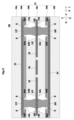
- Fig. 21 is a cross-sectional view of the electronic device 1 including the multilayer substrate 10.
- the electronic device 1 includes a multi-layer substrate 10 and a housing 100.
- the housing 100 houses the multi-layer substrate 10.
- the electronic device 1 is a wireless communication terminal such as a smartphone.
- the multi-layer substrate 10 is bent.
- the multilayer board according to the present invention is not limited to the multilayer boards 10, 10a to 10p, and may be modified within the scope of the invention.
- the structures of the multilayer boards 10, 10a to 10p may be combined in any manner.
- At least one of the materials of the insulator layer 16a (first insulator layer) and the insulator layer 16b (second insulator layer) may be liquid crystal polymer, polyimide, perfluoroalkoxyalkane, or polytetrafluoroethylene.
- the area of the first conductor layer 22a is smaller than the area of the upper end (the end on the positive side of the Z axis) of the first through hole h3a when viewed downward (the negative direction of the Z axis), or the area of the second conductor layer 25a is smaller than the area of the lower end (the end on the negative side of the Z axis) of the second through hole h3b when viewed downward (the negative direction of the Z axis).
- the first ground conductor layer 22 may be located on the upper main surface of the insulator layer 16a, or may be located above the upper main surface of the insulator layer 16a. In other words, the first ground conductor layer 22 does not have to be in contact with the upper main surface of the insulator layer 16a.
- the third ground conductor layer 25 may be located on the lower main surface of the insulator layer 16b, or may be located below the lower main surface of the insulator layer 16b. In other words, the third ground conductor layer 25 does not have to be in contact with the lower main surface of the insulator layer 16b.
- the space Sp1 may exist between the inner surface of the second through hole h3b and the center CP of the first interlayer connection conductor v3a on the vertical axis (Z axis).
- the melting point of the material of the first interlayer connection conductors v1 to v4 may be higher than the melting point of the solder used to mount the electronic components. This prevents the first interlayer connection conductors v1 to v4 from melting when the electronic components are mounted. This prevents deformation of the first interlayer connection conductors v1 to v4. As a result, fluctuations in the electrical characteristics of the multilayer substrate 10 are suppressed.
- the insulator layers 16a to 16d may be crimped after the insulator layers 16b and 16c are crimped.
- the thickness of the insulator layer 16a in the vertical axis is smaller than the thickness of the insulator layer 16b in the vertical axis.
- the thickness of the insulator layer 16a in the vertical axis may be equal to the thickness of the insulator layer 16b in the vertical axis, or may be greater than the thickness of the insulator layer 16b in the vertical axis.
- the thickness of the insulator layer 16d along the vertical axis is smaller than the thickness of the insulator layer 16c along the vertical axis.
- the thickness of the insulator layer 16d along the vertical axis may be equal to the thickness of the insulator layer 16c along the vertical axis, or may be greater than the thickness of the insulator layer 16c along the vertical axis.
- the size relationship of the through holes formed in the insulator layers 16a and 16b may be reversed.
- an adhesive layer may be provided between the insulator layer 16b and the insulator layer 16c.
- first interlayer connection conductor v3a and a portion of the first interlayer connection conductor v4a may overlap when viewed in a downward direction.
- the first interlayer connection conductor v3a and the first interlayer connection conductor v4a do not have to overlap when viewed in a downward direction.
- the material of the protective layers 18a and 18b may be the same as the material of the insulating layers 16a to 16f.
- the present invention has the following structure:
- the multilayer substrate includes a laminate, a first conductor layer, a second conductor layer, and a first interlayer connection conductor
- the laminate has a structure in which a plurality of insulator layers including a first insulator layer and a second insulator layer are laminated along a Z axis, Each of the first and second insulator layers has a positive and a negative principal surface, a positive principal surface of the second insulator layer in contact with a negative principal surface of the first insulator layer; the first conductor layer is located on the positive side of the Z-axis relative to the first insulator layer, the second conductor layer is located on the negative side of the Z axis relative to the second insulator layer,
- the first insulating layer is provided with a first through hole penetrating the first insulating layer along the Z-axis,
- the second insulating layer is provided with a second through hole penetrating the second insulating layer along the Z-axis, The second through hole overlaps with the first
- the space faces at least a part of an inner circumferential surface of the first through hole and faces at least a part of an inner circumferential surface of the second through hole.
- a multilayer substrate according to any one of (1) to (3).
- the first through hole has a tapered shape that narrows in the positive direction of the Z axis
- the second through hole has a tapered shape that narrows in the negative direction of the Z axis.
- the first interlayer connection conductor has an intermediate portion located between an end portion of the first interlayer connection conductor on a positive side of the Z-axis and an end portion of the first interlayer connection conductor on a negative side of the Z-axis, the first interlayer connection conductor has a first section having a tapered shape that becomes thinner from an end portion on the positive side of the Z axis toward the intermediate portion, and a second section having a tapered shape that becomes thinner from an end portion on the negative side of the Z axis toward the intermediate portion.
- a multilayer substrate according to any one of (1) to (5).
- an area of the first conductor layer is smaller than an area of an end of the first through hole on the positive side of the Z axis, or when viewed in the negative direction of the Z axis, an area of the second conductor layer is smaller than an area of an end of the second through hole on the negative side of the Z axis.
- a multilayer substrate according to any one of (1) to (7).
- the material of the first interlayer connection conductor is an alloy containing Sn.
- the melting point of the material of the first interlayer connection conductor is equal to or lower than the melting point of the solder used for mounting electronic components.
- the material of the first insulating layer and the material of the second insulating layer are flexible resins.
- the material of the first insulator layer is different from the material of the second insulator layer;
- At least one of the material of the first insulating layer and the material of the second insulating layer is a liquid crystal polymer, a polyimide, a perfluoroalkoxyalkane, or a polytetrafluoroethylene.
- a multilayer substrate according to any one of (1) to (13).
- the stack further includes a third insulator layer; the third insulator layer has a positive principal surface and a negative principal surface; a negative major surface of the third insulator layer in contact with a positive major surface of the first insulator layer;
- the second insulator layer is an adhesive layer that bonds the first insulator layer and the third insulator layer.
- a high-frequency signal having a frequency of 1 GHz or more and 1 THz or less is transmitted to the first conductor layer, the second conductor layer, and the first interlayer connection conductor, or a ground potential is connected to the first conductor layer, the second conductor layer, and the first interlayer connection conductor.
- the multilayer substrate further includes a second interlayer connection conductor,
- the plurality of insulator layers further includes a third insulator layer; the second interlayer connection conductor penetrates the third insulating layer along the Z-axis; There is no space between the second interlayer connection conductor and the third insulating layer.
- the laminate has a positive principal surface and a negative principal surface, a distance from the first insulator layer to a positive principal surface of the laminate is shorter than a distance from the third insulator layer to a positive principal surface of the laminate;
- the multilayer substrate has a first line section and a second line section aligned along an X-axis perpendicular to the Z-axis, the first insulating layer and the second insulating layer are located in the first line section and the second line section, the third insulating layer is located in the first line section and is not located in the second line section; A thickness of the first line section in the Z-axis direction is greater than a thickness of the second line section in the Z-axis direction.
- a multilayer substrate according to any one of (1) to (19) is provided. Electronic devices.
- (21) providing a first insulator layer and a second insulator layer having positive and negative major surfaces aligned along a Z-axis; a first through hole forming step of forming a first through hole penetrating the first insulator layer along the Z-axis; a second through hole forming step of forming a second through hole penetrating the second insulator layer along the Z-axis; a first interlayer connection conductor forming step of stacking the first insulator layer and the second insulator layer so that a negative principal surface of the first insulator layer and a positive principal surface of the second insulator layer are in contact with each other, and forming a first interlayer connection conductor extending along the Z-axis within the first through hole and the second through hole; Equipped with When viewed in a positive direction of the Z axis, an area of an end of the second through hole on the positive side of the Z axis is larger than an area of an end of the first through hole on the negative side of the Z axis,
- Multilayer board 12 Laminated body 16a to 16f: Insulator layer 18a, 18b: Protective layer 20: Signal conductor layer 22: First ground conductor layer 22a: First conductor layer 24: Second ground conductor layer 25: Third ground conductor layer 25a: Second conductor layers 26a, 26b: Mounting electrode 100: Housing A1: First section A2: Second section CP: Center DP: Bottom end E: Outer edge MP: Middle Parts Sp1, Sp2: space UP: upper end part h0: through holes h1a, h3a, h3d, h4d: first through holes h1b, h3b, h3c, h4c: second through holes h3e, h3f: third through holes v1 to v4, v3a, v3b, v4a, v4b: first interlayer connection conductors V1, V3a to V3c, V4a to V4c, V11a to V11
Landscapes
- Engineering & Computer Science (AREA)
- Microelectronics & Electronic Packaging (AREA)
- Manufacturing & Machinery (AREA)
- Physics & Mathematics (AREA)
- Electromagnetism (AREA)
- Production Of Multi-Layered Print Wiring Board (AREA)
Priority Applications (2)
| Application Number | Priority Date | Filing Date | Title |
|---|---|---|---|
| JP2025500714A JPWO2024171659A1 (https=) | 2023-02-16 | 2024-01-11 | |
| US19/294,739 US20250365857A1 (en) | 2023-02-16 | 2025-08-08 | Multilayer substrate, electronic device, and method for manufacturing multilayer substrate |
Applications Claiming Priority (2)
| Application Number | Priority Date | Filing Date | Title |
|---|---|---|---|
| JP2023-022143 | 2023-02-16 | ||
| JP2023022143 | 2023-02-16 |
Related Child Applications (1)
| Application Number | Title | Priority Date | Filing Date |
|---|---|---|---|
| US19/294,739 Continuation US20250365857A1 (en) | 2023-02-16 | 2025-08-08 | Multilayer substrate, electronic device, and method for manufacturing multilayer substrate |
Publications (1)
| Publication Number | Publication Date |
|---|---|
| WO2024171659A1 true WO2024171659A1 (ja) | 2024-08-22 |
Family
ID=92421531
Family Applications (1)
| Application Number | Title | Priority Date | Filing Date |
|---|---|---|---|
| PCT/JP2024/000392 Ceased WO2024171659A1 (ja) | 2023-02-16 | 2024-01-11 | 多層基板、電子機器及び多層基板の製造方法 |
Country Status (3)
| Country | Link |
|---|---|
| US (1) | US20250365857A1 (https=) |
| JP (1) | JPWO2024171659A1 (https=) |
| WO (1) | WO2024171659A1 (https=) |
Citations (7)
| Publication number | Priority date | Publication date | Assignee | Title |
|---|---|---|---|---|
| JPH0590750A (ja) * | 1991-03-25 | 1993-04-09 | Hughes Aircraft Co | 回路板の両面の相互接続方法 |
| KR20080107933A (ko) * | 2007-06-08 | 2008-12-11 | 삼성전기주식회사 | 도전성 페이스트 조성물 및 저온동시소성 세라믹 기판 |
| JP2011009694A (ja) * | 2009-05-27 | 2011-01-13 | Kyocera Corp | 配線基板およびプローブカードならびに電子装置 |
| JP2019160885A (ja) * | 2018-03-08 | 2019-09-19 | スタンレー電気株式会社 | 回路基板、電子回路装置、および、回路基板の製造方法 |
| US20200006233A1 (en) * | 2018-07-02 | 2020-01-02 | International Business Machines Corporation | Pin assemblies for plated vias |
| WO2020122180A1 (ja) * | 2018-12-13 | 2020-06-18 | 株式会社村田製作所 | 樹脂多層基板および電子機器 |
| JP2021097121A (ja) * | 2019-12-17 | 2021-06-24 | 日東電工株式会社 | 両面配線回路基板の製造方法および両面配線回路基板 |
-
2024
- 2024-01-11 JP JP2025500714A patent/JPWO2024171659A1/ja active Pending
- 2024-01-11 WO PCT/JP2024/000392 patent/WO2024171659A1/ja not_active Ceased
-
2025
- 2025-08-08 US US19/294,739 patent/US20250365857A1/en active Pending
Patent Citations (7)
| Publication number | Priority date | Publication date | Assignee | Title |
|---|---|---|---|---|
| JPH0590750A (ja) * | 1991-03-25 | 1993-04-09 | Hughes Aircraft Co | 回路板の両面の相互接続方法 |
| KR20080107933A (ko) * | 2007-06-08 | 2008-12-11 | 삼성전기주식회사 | 도전성 페이스트 조성물 및 저온동시소성 세라믹 기판 |
| JP2011009694A (ja) * | 2009-05-27 | 2011-01-13 | Kyocera Corp | 配線基板およびプローブカードならびに電子装置 |
| JP2019160885A (ja) * | 2018-03-08 | 2019-09-19 | スタンレー電気株式会社 | 回路基板、電子回路装置、および、回路基板の製造方法 |
| US20200006233A1 (en) * | 2018-07-02 | 2020-01-02 | International Business Machines Corporation | Pin assemblies for plated vias |
| WO2020122180A1 (ja) * | 2018-12-13 | 2020-06-18 | 株式会社村田製作所 | 樹脂多層基板および電子機器 |
| JP2021097121A (ja) * | 2019-12-17 | 2021-06-24 | 日東電工株式会社 | 両面配線回路基板の製造方法および両面配線回路基板 |
Also Published As
| Publication number | Publication date |
|---|---|
| US20250365857A1 (en) | 2025-11-27 |
| JPWO2024171659A1 (https=) | 2024-08-22 |
Similar Documents
| Publication | Publication Date | Title |
|---|---|---|
| JP7772040B2 (ja) | 伝送線路 | |
| US9059493B2 (en) | High-frequency signal line and electronic device | |
| US10028388B2 (en) | Component-embedded substrate | |
| WO2022113889A1 (ja) | 伝送線路及び電子機器 | |
| US9318786B2 (en) | High-frequency signal line and electronic device | |
| US12342452B2 (en) | Circuit board and electronic device | |
| US20240365477A1 (en) | Circuit board and method of producing circuit board | |
| JP6547833B2 (ja) | 多層基板、電子機器および多層基板の製造方法 | |
| US12431603B2 (en) | Multilayer substrate and manufacturing method therefor | |
| WO2024171659A1 (ja) | 多層基板、電子機器及び多層基板の製造方法 | |
| US12464653B2 (en) | Circuit board and electronic-component-equipped circuit board | |
| JPWO2024171659A5 (https=) | ||
| US12191553B2 (en) | Transmission line | |
| US12273994B2 (en) | Multilayer substrate module with filter function | |
| JP7420315B2 (ja) | アンテナ素子、電子機器及びアンテナ素子の製造方法 | |
| JP2015185550A (ja) | 多層高周波基板、アンテナ装置 | |
| JP7827160B2 (ja) | アンテナモジュール | |
| JP7409493B2 (ja) | 信号伝送線路及び信号伝送線路の製造方法 | |
| JP7794328B2 (ja) | 多層基板 | |
| CN220210656U (zh) | 电路基板以及电子设备 | |
| US20250240874A1 (en) | Multilayer substrate and method for manufacturing multilayer substrate | |
| JP2014175829A (ja) | 伝送線路、アンテナ装置及び伝送線路製造方法 | |
| WO2022270294A1 (ja) | 多層基板、多層基板モジュール及び電子機器 | |
| WO2024195375A1 (ja) | 多層基板及び電子機器 | |
| WO2022118810A1 (ja) | 伝送線路及び電子機器 |
Legal Events
| Date | Code | Title | Description |
|---|---|---|---|
| 121 | Ep: the epo has been informed by wipo that ep was designated in this application |
Ref document number: 24756511 Country of ref document: EP Kind code of ref document: A1 |
|
| ENP | Entry into the national phase |
Ref document number: 2025500714 Country of ref document: JP Kind code of ref document: A |
|
| WWE | Wipo information: entry into national phase |
Ref document number: 2025500714 Country of ref document: JP |
|
| NENP | Non-entry into the national phase |
Ref country code: DE |
|
| 122 | Ep: pct application non-entry in european phase |
Ref document number: 24756511 Country of ref document: EP Kind code of ref document: A1 |