WO2024166857A1 - 電子部品 - Google Patents
電子部品 Download PDFInfo
- Publication number
- WO2024166857A1 WO2024166857A1 PCT/JP2024/003686 JP2024003686W WO2024166857A1 WO 2024166857 A1 WO2024166857 A1 WO 2024166857A1 JP 2024003686 W JP2024003686 W JP 2024003686W WO 2024166857 A1 WO2024166857 A1 WO 2024166857A1
- Authority
- WO
- WIPO (PCT)
- Prior art keywords
- magnetic
- electronic component
- wiring
- sintered
- component according
- Prior art date
- Legal status (The legal status is an assumption and is not a legal conclusion. Google has not performed a legal analysis and makes no representation as to the accuracy of the status listed.)
- Ceased
Links
Images





Classifications
-
- H—ELECTRICITY
- H01—ELECTRIC ELEMENTS
- H01F—MAGNETS; INDUCTANCES; TRANSFORMERS; SELECTION OF MATERIALS FOR THEIR MAGNETIC PROPERTIES
- H01F1/00—Magnets or magnetic bodies characterised by the magnetic materials therefor; Selection of materials for their magnetic properties
- H01F1/01—Magnets or magnetic bodies characterised by the magnetic materials therefor; Selection of materials for their magnetic properties of inorganic materials
- H01F1/03—Magnets or magnetic bodies characterised by the magnetic materials therefor; Selection of materials for their magnetic properties of inorganic materials characterised by their coercivity
- H01F1/12—Magnets or magnetic bodies characterised by the magnetic materials therefor; Selection of materials for their magnetic properties of inorganic materials characterised by their coercivity of soft-magnetic materials
- H01F1/14—Magnets or magnetic bodies characterised by the magnetic materials therefor; Selection of materials for their magnetic properties of inorganic materials characterised by their coercivity of soft-magnetic materials metals or alloys
- H01F1/147—Alloys characterised by their composition
-
- H—ELECTRICITY
- H01—ELECTRIC ELEMENTS
- H01F—MAGNETS; INDUCTANCES; TRANSFORMERS; SELECTION OF MATERIALS FOR THEIR MAGNETIC PROPERTIES
- H01F17/00—Fixed inductances of the signal type
- H01F17/04—Fixed inductances of the signal type with magnetic core
-
- H—ELECTRICITY
- H01—ELECTRIC ELEMENTS
- H01F—MAGNETS; INDUCTANCES; TRANSFORMERS; SELECTION OF MATERIALS FOR THEIR MAGNETIC PROPERTIES
- H01F27/00—Details of transformers or inductances, in general
- H01F27/24—Magnetic cores
- H01F27/255—Magnetic cores made from particles
-
- H—ELECTRICITY
- H01—ELECTRIC ELEMENTS
- H01F—MAGNETS; INDUCTANCES; TRANSFORMERS; SELECTION OF MATERIALS FOR THEIR MAGNETIC PROPERTIES
- H01F27/00—Details of transformers or inductances, in general
- H01F27/28—Coils; Windings; Conductive connections
- H01F27/29—Terminals; Tapping arrangements for signal inductances
-
- H—ELECTRICITY
- H01—ELECTRIC ELEMENTS
- H01F—MAGNETS; INDUCTANCES; TRANSFORMERS; SELECTION OF MATERIALS FOR THEIR MAGNETIC PROPERTIES
- H01F27/00—Details of transformers or inductances, in general
- H01F27/28—Coils; Windings; Conductive connections
- H01F27/32—Insulating of coils, windings, or parts thereof
Definitions
- This disclosure relates to electronic components.
- the inductor components as electronic components can be used in various power supply circuits.
- the inductor components include a base body and wiring located inside the base body.
- the base body can be a magnetic composite body having inorganic filler and resin as magnetic materials (see Patent Document 1).
- the characteristics of the electronic component are improved by increasing the filling rate of the magnetic material in the magnetic composite body, i.e., the metal magnetic particles.
- the metal magnetic particles also contain resin, there is a limit to how much the filling rate of the metal magnetic particles can be increased, and localized concentration of magnetic flux can occur between the metal magnetic particles. This makes the magnetic body more susceptible to magnetic saturation, which may result in a decrease in the magnetic energy that can be stored.
- magnetic composite bodies are not sintered, the distortion applied to the metal magnetic body during molding is not alleviated, which may lead to a decrease in magnetic permeability.
- the purpose of this disclosure is to provide electronic components that can improve inductance and magnetic energy.
- the present disclosure provides an electronic component comprising a base body including one or more sintered bodies and wiring provided within the base body, the sintered bodies being made of a metallic magnetic material, at least one of the sintered bodies including a first magnetic portion having a porosity of 0% or more and 6.0% or less and a saturation magnetic flux density (Bs) of 1.89 T or more and 2.26 T or less, and the wiring being disposed within the first magnetic portion.
- This disclosure makes it possible to improve the inductance and magnetic energy of electronic components.
- FIG. 1 is a perspective view illustrating an electronic component according to a first embodiment of the present disclosure.
- 1B is a schematic cross-sectional view taken along line a-a in FIG. 1A.
- FIG. 11 is a perspective view illustrating an electronic component according to a second embodiment of the present disclosure.
- FIG. 11 is a perspective view illustrating an electronic component according to a third embodiment of the present disclosure.
- 2B is a schematic cross-sectional view taken along line bb in FIG. 2A.
- FIG. 11 is a perspective view illustrating an electronic component according to a fourth embodiment of the present disclosure. 4 is a schematic cross-sectional view taken along line cc in FIG. 3.
- FIG. 3 is a schematic cross-sectional view taken along line cc in FIG. 3.
- FIG. 13 is a perspective view showing a schematic diagram of an electronic component (first large magnetic region + two wirings) according to a fifth embodiment of the present disclosure.
- 6 is a schematic cross-sectional view taken along line dd in FIG. 5 .
- FIG. 13 is a perspective view illustrating an electronic component (in a first magnetic region plus two wirings) according to a sixth embodiment of the present disclosure.
- 8 is a schematic cross-sectional view taken along line ee in FIG. 7.
- FIG. 13 is a perspective view showing a schematic diagram of an electronic component (first small magnetic region + two wirings) according to a seventh embodiment of the present disclosure.
- 10 is a schematic cross-sectional view taken along line ff in FIG. 9 .
- FIG. 9 is a schematic cross-sectional view taken along line ff in FIG. 9 .
- FIG. 13 is a perspective view showing a schematic diagram of an electronic component (four external electrodes and two wirings) according to an eighth embodiment of the present disclosure.
- 12 is a schematic cross-sectional view taken along line gg in FIG. 11 .
- FIG. 13 is a perspective view showing a schematic diagram of an electronic component (wiring connected to a bottom electrode) according to a ninth embodiment of the present disclosure.
- 14 is a schematic cross-sectional view taken along line h-h in FIG. 13.
- 14 is a schematic cross-sectional view taken along line ii in FIG. 13.
- FIG. 1 is a perspective view showing a schematic diagram of a conventional electronic component (including a magnetic composite body and wiring).
- 17 is a schematic cross-sectional view taken along line j-j in FIG. 16.
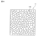
- FIG. 2 is an enlarged cross-sectional view showing a schematic diagram of a sintered body of an element body.
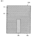
- FIG. 18 is an enlarged cross-sectional view showing a schematic diagram of a magnetic composite body
- FIG. 1A is a perspective view showing a schematic diagram of an electronic component according to embodiment 1 of the present disclosure.
- FIG. 1B is a schematic cross-sectional view taken along line a-a in FIG. 1A.
- the electronic component 100 of embodiment 1 includes a base body 10, wiring 20, and external electrodes 30, 40.
- the base body 10 includes a sintered body 11, which may be made of a metallic magnetic material.
- the base body 10 may have a hexahedral structure.
- the sintered body 11 may be at least one selected from the group consisting of iron, an alloy containing iron and nickel, an alloy containing iron and cobalt, and an alloy containing iron and silicon.
- an insulating coating layer 60 may be provided that covers the surface of the base body 10 except for the external electrodes 30, 40.
- the wiring 20 is provided within the element body 10 and is made of a conductive material.
- the wiring 20 may be at least one type selected from the group consisting of, for example, silver, copper, aluminum, etc. As an example of the form of the wiring 20, it may be straight wiring as shown in FIG. 1A. Without being limited to this, the wiring may be coil-shaped wiring.
- the external electrodes 30, 40 are provided on the surface of the element body 10. Materials for the external electrodes 30, 40 may include, for example, silver, copper, nickel, etc. These external electrodes are connected to both ends of the wiring 20, respectively, and are arranged facing each other at a distance across the element body 10.
- the sintered body 11 has a first magnetic portion 12, and the wiring 20 is disposed within the first magnetic portion 12. From another perspective, the wiring 20 is surrounded by the first magnetic portion 12. Specifically, the portion of the wiring 20 other than both ends connected to the external electrodes 30, 40 is disposed within the first magnetic portion 12. From yet another perspective, when viewed in a cross section perpendicular to the extension direction of the wiring 20, the first magnetic portion 12 is present around the entire periphery of the cross-sectional portion of the wiring 20.
- the above-mentioned first magnetic portion 12 refers to the region of the sintered body 11 with a void ratio of 0% to 6.0% and a saturation magnetic flux density (Bs) of 1.89 T to 2.26 T.
- the first magnetic portion constituting the sintered body 11 has a high Bs of 1.89 T to 2.26 T, which makes it possible to suppress magnetic saturation compared to when a magnetic composite body is used for the base body 10'. As a result, it is possible to suppress the decrease in storable magnetic energy, and as a result, the DC superposition characteristics are improved.
- the sintered body 11 Since the void ratio of the first magnetic portion is 6.0% or less, the sintered body 11 has a high-density region, and the space factor of the metal magnetic body can be increased compared to when a magnetic composite body is used for the base body 10' (see Figures 16, 17, and 19). As a result, the decrease in storable magnetic energy can be suppressed, and the DC superposition characteristics are improved.
- the void ratio of the first magnetic portion is low, local concentration of magnetic flux can be suppressed, and magnetic saturation can be suppressed, improving the DC superposition characteristics.
- the base body 10 since the base body 10 includes the sintered body 11, the stress distortion that occurred in the metal magnetic body during molding is alleviated, and the magnetic permeability is improved. This improves the inductance (L value).
- I sat the DC current value when L drops by 30% from the initial value
- I sat the DC current value when L drops by 30% from the initial value
- the first magnetic part 12 which has a high saturation magnetic flux density, can be positioned so as to surround the wiring 20. This makes it possible to effectively suppress magnetic saturation and effectively improve the DC superposition characteristics.
- the base body 10 may further have a first insulating layer 13.
- This first insulating layer 13 may be continuous in a layered form from one side of the sintered body 11 to the other side in a direction intersecting the stacking direction L. With this form, two or more sintered bodies 11 separated by the first insulating layer 13 may be provided.
- the base body 10 has two or more sintered bodies 11 and a first insulating layer 13, and adjacent sintered bodies 11 and the other sintered body can be stacked with the first insulating layer 13 sandwiched between them.
- all of the partitioned two or more sintered bodies 11 can be composed of the first magnetic part 12. That is, each of the two or more sintered bodies 11 has a first magnetic part or is composed of the first magnetic part. Therefore, the first insulating layer 13 can be in contact with the first magnetic parts of the two or more sintered bodies (i.e., two sintered bodies 11 each composed of the first magnetic part 12).
- Each sintered body 11 itself has at least one metal magnetic sintered layer, and the metal magnetic sintered layer and the first insulating layer 13 constituting each sintered body 11 can be stacked along the stacking direction.
- the metal magnetic sintered layer and the first insulating layer 13 constituting each sintered body 11 can be stacked along the stacking direction.
- the first insulating layer 13 By providing the above-mentioned first insulating layer 13, a magnetic gap function can be provided compared to when it is not provided. It is also preferable that the first insulating layer 13 is non-magnetic. This makes it possible to improve the DC superposition characteristics by reducing the magnetic permeability of the base body 10. However, without being limited to this, the first insulating layer 13 can be a low-permeability insulating layer that is not non-magnetic but has a magnetic permeability lower than that of the sintered body 11. In this case, inductance can also be improved compared to when it is non-magnetic.
- first insulating layers 13 may be provided, spaced apart from each other.
- the base body 10 has four sintered bodies 11.
- the wiring 20 is disposed between the first insulating layers 13, and the base body 10 may include three or more sintered bodies 11.
- a layered structure can be formed in which two or more sintered bodies 11 and two or more first insulating layers 13 are alternately stacked.
- the two sintered bodies 11 located on either side of the wiring can have a smaller width than the other sintered bodies.
- the two sintered bodies 11 can be arranged side by side with the wiring 20 in between in a direction intersecting the stacking direction L.
- the first external electrode 30 and the second external electrode 40 are arranged on the surfaces of different sintered bodies 11.
- the element body 10 can further have a second insulating layer 50.
- the first external electrode 30 and the second external electrode 40 are respectively arranged on the surfaces of adjacent sintered bodies 11, with the first external electrode 30 arranged on the surface of the sintered body 11 on one side and the second external electrode 30 arranged on the surface of the sintered body 11 on the other side.
- a second insulating layer 50 can be arranged between one sintered body 11 on which the first external electrode 30 is arranged and the sintered body 11 on which the second external electrode 40 is arranged.
- the second insulating layer 50 may be a slit-shaped tangible object that extends in a direction intersecting, for example, perpendicular to, the extension direction of the first insulating layer 13. Note that the second insulating layer 50 is not disposed so as to penetrate into the wiring located inside the element body 10 and divide the wiring.
- the first magnetic portion surrounds everything except the via conductor of the wiring, and preferably also surrounds the via conductor. Also, when there are multiple first magnetic portions, the magnetic permeability may or may not be the same.
- FIG. 1C is a cross-sectional view showing a schematic diagram of an electronic component according to embodiment 2 of the present disclosure.
- the embodiment shown in FIG. 1C is a modified version of the embodiment shown in FIG. 1B.
- embodiment 2 differs in that wiring 20 covered with an insulator 15 is provided.
- the wiring 20 is directly surrounded by the insulator 15, except for the two ends connected to the external electrodes 30, 40.
- This allows the insulator 15 to function as a magnetic gap.
- the insulator 15 is non-magnetic. This makes it possible to improve the DC superposition characteristics by reducing the magnetic permeability of the element body 10.
- the insulator 15 can be a low-permeability insulator that is not non-magnetic and has a magnetic permeability lower than that of the sintered body 11. In this case, inductance can also be improved compared to the non-magnetic case.
- FIG. 2A is a perspective view showing a schematic diagram of an electronic component according to a third embodiment of the present disclosure.
- FIG. 2B is a schematic cross-sectional view taken along line b-b in FIG. 2A.
- the third embodiment differs from the first embodiment in that at least one sintered body 11A has a high permeability portion 14A with a relative permeability of 700 or more.
- Each magnetic portion may be composed of at least one metal magnetic sintered layer.
- the first insulating layer 13A may be disposed within the first magnetic portion 12A. Since the high permeability portion 14A has a high relative permeability, the inductance can be further improved compared to the first embodiment (a configuration without a high permeability portion).
- the first magnetic portion refers to a region in the sintered body 11A where the void ratio is 0% or more and 6.0% or less and the saturation magnetic flux density (Bs) is 1.89 T or more and 2.26 T or less.
- the high permeability portion refers to a region in the sintered body 11A where the relative permeability is 700 or more.
- the wiring 20A can be provided within the first magnetic part 12A.
- the first magnetic part 12A which has a high saturation magnetic flux density, can be positioned in the vicinity of the wiring 20A. This makes it possible to effectively suppress magnetic saturation and effectively improve the DC superposition characteristics.
- the term "sintered body of a metal magnetic material” refers to a sintered body of metal magnetic particles, as shown in FIG. 18, which is an enlarged view of the dotted circle area in FIG. 1B and FIG. 2B, and is composed of non-uniform metal magnetic particles, as compared with a conventional magnetic composite body (see FIG. 19) having a uniform (e.g., substantially circular) metal magnetic particles.
- the region of the sintered body of a metal magnetic material in which the void ratio is 0% or more and 6.0% or less and the saturation magnetic flux density (Bs) is 1.89 T or more and 2.26 T or less is called the first magnetic part.
- the first magnetic part may be a part of a sintered body of a metal magnetic material, or the entire sintered body of a metal magnetic material may be the first magnetic part. It is preferable that the grain boundary phase of the metal magnetic particles has a higher resistance than the resistance of the metal magnetic particle part. This can reduce eddy current loss, which increases with increasing frequency.
- the grain boundary phase of the metal magnetic particles preferably contains a metal oxide or metal nitride in which a non-magnetic metal is oxidized or nitrided. In this disclosure, silicon, which is called a semimetal, is treated as a metal.
- FIG. 3 is a perspective view showing a schematic diagram of an electronic component according to a fourth embodiment of the present disclosure.
- FIG. 4 is a schematic cross-sectional view taken along line c-c in FIG. 3.
- the multiple sintered bodies have a first magnetic portion 12B and a high magnetic permeability portion 14B, and each magnetic portion can be composed of at least one metal magnetic sintered layer.
- the fourth embodiment differs from the third embodiment in that the first insulating layer 13B is disposed not only in the first magnetic portion 12B but also in the high magnetic permeability portion 14B, and the first insulating layer 13B and the metal magnetic sintered layers constituting each magnetic portion are alternately stacked.
- the number of first insulating layers is increased, so that the first insulating layers 13B can function more effectively as magnetic gaps within the base body 10B, and the magnetic permeability of the base body 10B can be further reduced, thereby improving the DC superposition characteristics.
- FIG. 5 is a perspective view showing a schematic of an electronic component (first large magnetic region + 2 wires) according to embodiment 5 of the present disclosure.
- FIG. 6 is a schematic cross-sectional view taken along line d-d in FIG. 5.
- FIG. 7 is a perspective view showing a schematic of an electronic component (first medium magnetic region + 2 wires) according to embodiment 6 of the present disclosure.
- FIG. 8 is a schematic cross-sectional view taken along line ee in FIG. 7.
- FIG. 9 is a perspective view showing a schematic of an electronic component (first small magnetic region + 2 wires) according to embodiment 7 of the present disclosure.
- FIG. 10 is a schematic cross-sectional view taken along line f-f in FIG. 9.
- the fifth embodiment is different from the first embodiment in that it has two or more wirings 20C.
- I sat the direct current value when L is reduced by 30% from the initial value
- I sat the direct current value when L is reduced by 30% from the initial value
- the number of layers of the first magnetic portion in the fifth embodiment shown in Fig. 5 and Fig. 6 is greater than those in the sixth and seventh embodiments.
- the first magnetic portion is a region with a high Bs, and the greater number of layers of the first magnetic portion increases I sat and can increase the magnetic energy. This makes it possible to further suppress magnetic saturation and further improve the DC bias characteristics.
- FIG. 11 is a perspective view showing a schematic diagram of an electronic component (four external electrodes + two wirings) according to an eighth embodiment of the present disclosure.
- FIG. 12 is a schematic cross-sectional view taken along line g-g in FIG. 11.
- Embodiment 8 differs from embodiment 1 in that two external electrodes 31F, 32F are arranged spaced apart on one side of element body 10F, and two external electrodes 41F, 42F are arranged spaced apart on the other side of element body 10F.
- two wirings 21F, 22F are provided as wiring, and both ends of first wiring 21F can be connected to mutually opposing external electrodes 31F, 41F, respectively.
- Both ends of second wiring 22F can be connected to mutually opposing external electrodes 32F, 42F, respectively.
- multiple inductor functions can be provided in electronic component 100F.
- FIG. 13 is a perspective view showing a schematic diagram of an electronic component (wiring connected to an external electrode provided on the bottom surface) according to a ninth embodiment of the present disclosure.
- FIG. 14 is a schematic cross-sectional view taken along line h-h in FIG. 13.
- FIG. 15 is a schematic cross-sectional view taken along line i-i in FIG. 13.
- the external electrode provided on the bottom surface is referred to as a bottom electrode.
- Embodiment 9 differs from embodiment 1 in that the external electrodes 30G, 40G are bottom electrodes.
- the wiring 20G located within the base body 10G has, for example, a bent shape. Both ends of the wiring 20G can extend to the bottom side of the electronic component 100G and be connected to the external electrodes 30G, 40G, which serve as bottom electrodes.
- By adopting such a bottom electrode structure it is possible to further improve the inductance. Without being bound by a particular theory, it is believed that this is due to the fact that the direction of the magnetic field formed by the wiring 20G extending to the bottom side is approximately the same as the longitudinal extension direction of the sintered body 11G.
- Magnetic metal particles having a D50 particle size of about 0.40 ⁇ m or more and 3.10 ⁇ m or less are prepared.
- ⁇ Preparation process of metal magnetic paste> After preparing the metal magnetic particles, the metal magnetic particles, varnish, a solvent (e.g., terpineol), etc. are mixed in a stirrer, and then a dispersion process is performed in a roll mill to obtain a metal magnetic paste.
- a solvent e.g., terpineol
- Non-magnetic insulating particles having a D50 particle size of about 0.1 ⁇ m to 0.5 ⁇ m are prepared. Then, the insulating particles, varnish, and a solvent (e.g., terpineol) are mixed in a stirrer. Then, a dispersion process is performed in a roll mill to obtain an insulating paste.
- the non-magnetic insulating material used in the insulating paste may be, for example, a mixture of alumina, silica, glass, or a dielectric material such as calcium zirconate, strontium zirconate, and/or barium zirconate with borosilicate glass or the like.
- Conductive particles with a D50 particle size of 1 ⁇ m to 5 ⁇ m are mixed with a varnish and a solvent (e.g., terpineol) in a stirrer. Dispersion is then performed in a roll mill to obtain a wiring paste. Silver particles or the like can be selected as the conductive particles.
- ⁇ Preparation step of unfired laminate> After preparing each paste, the above-mentioned metal magnetic paste is used to form a metal magnetic material layer of a predetermined thickness by, for example, screen printing, and then dried. After drying, slit grooves of a predetermined width are formed by laser processing, and the above-mentioned insulating paste is filled into the slit grooves by screen printing or the like, and then dried. Note that the slit grooves are not limited to post-processing by laser processing, and may be patterned in advance using a screen printing plate or the like.
- an insulating layer of a specified thickness is formed on the metal magnetic layer using the above insulating paste by screen printing and drying.
- the insulating paste used to form the insulating layer may be of a different type from the insulating paste filled into the slit grooves.
- wiring paste is used to form wiring in the desired shape (for example, straight, coiled, meandering, etc.) by screen printing.
- Coiled wiring refers to wiring with a circular wiring portion.
- via patterns that connect wiring patterns to each other are formed on multiple metal magnetic layers using wiring paste.
- the via pattern can be formed by first forming holes in the metal magnetic layer by laser processing or the like and filling them with wiring paste.
- an insulating layer may be further formed on top of it. The formation of the above metal magnetic material layer and, optionally, the formation of an insulating layer are repeated to obtain an unsintered laminate.
- the number of insulating layers may be reduced or eliminated. This makes it possible to adjust the balance between the L value and the DC superposition characteristics.
- the type of metal magnetic paste used in the above process can be changed midway depending on the metal magnetic material layer being formed.
- a screen printing layer formed using a screen printing method is laminated, but this is not limited to this, and the product can also be produced by preparing separate sheets and laminating the sheets.
- the outer surface of the fired laminate may be coated with an insulating resin, the coating may be removed from the area where the wiring and the external electrodes are to be connected with a laser, and then a plating process may be performed to form external electrodes.
- the material of the external electrodes may be, for example, silver.
- the above is based on the premise that a non-magnetic insulating layer is formed, but by extending the time that the maximum temperature (top firing temperature) during the above firing is held, the metal magnetic material components can be diffused from the metal magnetic layer into the non-magnetic insulating layer, resulting in an insulating layer with low magnetic permeability and some magnetic properties.
- the metal magnetic particles, varnish (resin type: ethyl cellulose, product name: Ethocel), and terpineol as a solvent were mixed in a mortar, the paste was oven-dried to remove the solvent, and the dried material was passed through a mesh to produce granulated powder.
- the granulated powder was pressurized at 120 MPa for 2 minutes while heated to 80°C to produce a toroidal core and a cylindrical sample.
- the mixture was degreased in a nitrogen atmosphere and fired at 900°C for 60 minutes in a reducing atmosphere of H2 : 3% / N2 : 97%, to obtain a toroidal core and a cylindrical sample made of a sintered body.
- the toroidal core was wound and the magnetic permeability ⁇ (100 Hz) was measured using an impedance analyzer E4990A (Keysight).
- the cylindrical sample was measured using a vibration sample magnetometer VSM-5 (Toei Kogyo Co., Ltd.) to measure the saturation magnetic flux density Bs (16000 Oe).
- the measured ⁇ and Bs were entered into the following formula to calculate the B-H data.
- B Bs ⁇ tanh(4 ⁇ 10-7 ⁇ H/Bs)
- the Bs was calculated using the density of the metal material alone (Fe: 7.87 g/cm 3 , Ni: 8.9 g/cm 3 , Co: 8.9 g/cm 3 ) and the alloy density calculated from the composition ratio of each alloy.
- the calculated alloy densities are as follows: Fe50Co: 8.37g/cm 3 , Fe10Ni30Co: 8.26g/cm 3 , Fe10Ni20Co: 8.16g/cm 3 , Fe20Ni: 8.06g/cm 3 , Fe45Ni: 8.31g/cm 3
- all wiring other than the magnetic body can be removed, and the magnetic body can be processed into a shape suitable for measurement with a vibrating sample magnetometer, and then measurement can be performed.
- the alloy density used to calculate Bs can be calculated using the alloy composition determined by a separate composition analysis, using the above-mentioned calculation.
- Comparative Example Metal magnetic particles, varnish (product name: Ethocel), and terpineol as a solvent were mixed in a mortar, and the paste was oven-dried to remove the solvent, and the dried product was passed through a mesh to produce granulated powder.
- the granulated powder was pressurized at 120 MPa for 2 minutes while heated to 80°C to produce a toroidal core and a cylindrical sample.
- the toroidal core was then degreased in air and fired at 650°C for 60 minutes in air.
- the voids in the fired toroidal core were then impregnated with epoxy resin and thermally cured to obtain a toroidal core made of a composite material.
- the toroidal core was then wound, and the magnetic permeability ⁇ (100 Hz) was measured using an impedance analyzer E4990A (manufactured by Keysight).
- the filling rate of the metal magnetic particles in the composite material was determined by the following method. Specifically, each sintered sample was resin-solidified, polished with a polishing device Tegramin-25 (manufactured by Struers), and ion milled with an ion milling device IM-3000 (manufactured by Hitachi High-Technologies Corporation). SEM images and optionally element mapping images were then obtained using a field emission scanning electron microscope SU8230 (manufactured by Hitachi High-Technologies Corporation). The imaging magnification was 2000x. These acquired images were analyzed using image analysis software WinROOF2021 (manufactured by Mitani Shoji Co., Ltd.) to calculate the filling rate. The filling rate was determined as the average value of the analysis values at three arbitrary locations.
- the filling rates for different types of metal magnetic particles were as follows: ⁇ Fe50Co: Filling rate 60% ⁇ Fe10Ni20Co: Filling rate 62% ⁇ Fe45Ni: Filling rate 71%
- the Bs of the composite material was calculated by multiplying this filling rate by the Bs measured for the above-mentioned sintered body.
- ⁇ Fe50Co: 2.33 ⁇ 0.60 1.40T
- ⁇ Fe45Ni: 1.57 ⁇ 0.71 1.11T
- the values calculated above were used for the B-H curve of the magnetic material. Note that the B-H curve used portions with relative permeability ⁇ r of 1 or more so that it would not fall below the permeability of a vacuum, and was then extrapolated to the permeability of a vacuum using the functions of Femtet2022.
- the wiring material was silver.
- ⁇ Laminate model> For the laminate model, 30 layers of sintered bodies (longitudinal dimension (L)/width dimension (W)/height (T) (same below): 1.0 mm/0.5 mm/0.02 mm) and 29 layers of non-magnetic insulating layers (L/W/t: 1.0 mm/0.5 mm/0.001 mm) were alternately laminated to form a hexahedral base body with L/W/T: 1.0 mm/0.5 mm/0.629 mm.
- a straight silver wiring (width/thickness/length: 0.0625 mm/0.02 mm/1.0 mm) was formed in the center of the W dimension.
- a non-magnetic second insulating layer (width 0.01 mm) was formed in the center of the L dimension, positioned to provide two sintered bodies between two external electrodes.
- Comparative Example 1 Sintered bodies of 1st to 30th layers (having neither the first magnetic portion nor the high magnetic permeability portion)
- Examples 1 to 3 1st to 30th layers of sintered compacts were used as the first magnetic part.
- Comparative Example 2 1st to 30th layers of sintered compacts were used as the high permeability part.
- Example 4 The five sintered layers, the 14th to 18th layers, were used as the first magnetic part, and the other 25 layers were used as the high permeability part.
- Comparative Examples 3 to 6 a composite material body with L/W/T of 1.0 mm/0.5 mm/0.629 mm was formed.
- Examples 1 to 4 and Comparative Examples 1 to 6 can be manufactured through the following process.
- metal magnetic particles having a D50 particle size of 0.40 ⁇ m were prepared, and then the metal magnetic particles, varnish, and terpineol as a solvent were mixed in a stirrer. After that, a dispersion process was performed in a roll mill to obtain a metal magnetic paste.
- Non-magnetic insulating particles of alumina and borosilicate glass with a D50 particle size of about 0.1 to 0.5 ⁇ m were prepared. Then, these insulating particles were mixed with varnish and terpineol as a solvent in a stirrer. After that, a dispersion process was performed in a roll mill to obtain an insulating paste.
- ⁇ Preparation step of unfired laminate> After preparing each paste, the above-mentioned metal magnetic paste was used to form a metal magnetic layer of a predetermined thickness by screen printing, which was then dried. After drying, a slit groove of a predetermined width was formed by laser processing, and the insulating paste was filled into the slit groove by screen printing, which was then dried.
- an insulating layer of a specified thickness is formed on the metal magnetic layer using the above insulating paste by screen printing and drying.
- the insulating paste used to form the insulating layer may be of a different type from the insulating paste filled into the slit grooves.
- the outer surface of the sintered body is coated with an insulating resin, the coating at the portion where the wiring and the external electrodes are to be connected is removed with a laser, and then a plating process is performed to form the external electrodes. In this manner, an electronic component is obtained.
- the material of the external electrodes can be, for example, silver.
- the measurement results for the above were as follows.
- Table 1 shows the results of measurements taken for each item, rather than a simulation, produced by actually producing a sintered body by firing the metal magnetic paste, as explained in the sections ⁇ Metal magnetic paste preparation process> and ⁇ Singulation and firing process of unfired laminate>.
- the relative permeability and Bs in Table 2 are also the results of measurements taken from the material that was actually produced.
- the measurement results for Li, Isat and magnetic energy in Table 2 are based on a simulation calculated from the above actual measurement data.
- Example 4 when Bs was in the range of 1.89 T to 2.26 T and the relative permeability was 63 to 115, the conditions of Li of 9 nH or more and magnetic energy of 320 ⁇ 10 -9 (J) or more were satisfied.
- the first magnetic part had the same permeability and Bs as in Example 2, while the high permeability part other than the first magnetic part had a large permeability and a small Bs. In this case, Li was larger and the magnetic energy was lower than in Example 2, but the overall conditions of Li of 9 nH or more and magnetic energy of 320 ⁇ 10 -9 (J) or more were satisfied.
- Comparative Example 1 the magnetic permeability was less than Li:9 nH, and the L value judgment was not met.
- the magnetic energy was 56 ⁇ 10 ⁇ 9 (J) due to the Bs being 1.57 T, and the magnetic energy condition was not satisfied.
- the porosity was the average value of the analysis values at three arbitrary locations.
- the average value is taken for the analysis values at three arbitrary locations at a position 1 times the wiring thickness upward from the top surface of the internal wiring and three arbitrary locations at a position 1 times the wiring thickness downward from the bottom surface of the internal wiring, a total of six locations.
- the simulation model was as follows.
- a straight silver wiring (width/thickness/length: 0.0625 mm/0.02 mm/1.0 mm) was formed inside an element body with L/W/T: 1.0 mm/0.5 mm/0.629 mm, 0.315 mm from the bottom surface and in the center of the W dimension.
- a non-magnetic insulating layer (width 0.01 mm) was formed between two adjacent sintered bodies at the center of the L dimension. Then, inside the base body, the parts excluding the straight wiring and the non-magnetic insulating layer were made into a sintered body. That is, in Examples 5 to 8, the entire sintered body except for the non-magnetic insulating layer was made into the first magnetic part, and in Comparative Example 7, the entire sintered body except for the non-magnetic insulating layer was made into a simple sintered body that did not belong to either the high permeability part or the first magnetic part.
- the measurement results for the above were as follows.
- Example 4 The five sintered layers, 14th to 18th layers, were used as the first magnetic portion, and the remaining 25 layers were used as the high magnetic permeability portion.
- Example 9 The nine sintered layers, the 12th to 20th layers from the bottom, were used as the first magnetic portion, and the other layers were used as the high magnetic permeability portion.
- Example 10 The seven sintered layers, the 13th to 19th layers from the bottom, were used as the first magnetic portion, and the other layers were used as the high magnetic permeability portion.
- Example 11 The five sintered layers, the 14th to 18th layers from the bottom, were used as the first magnetic portion, and the other layers were used as the high magnetic permeability portion.
- the measurement results for the above were as follows.
- Example 9 the number of layers of the first magnetic part in Example 9 is greater than those in Examples 10 and 11.
- the first magnetic part is a region with a high Bs, and it was found that the greater number of layers of this first magnetic part results in a larger I sat and higher magnetic energy.
- Example 10 differs in having two wirings. It was found that the increased number of wirings allows magnetic coupling to be formed, resulting in a larger I sat .
- Example 12 The following simulation model was used. Specifically, 30 layers of sintered metal magnetic material (L/W/t: 1.0 mm/0.5 mm/0.02 mm) and 29 layers of non-magnetic insulating layers (L/W/t: 1.0 mm/0.5 mm/0.001 mm) were alternately stacked to form a hexahedral element with L/W/T: 1.0 mm/0.5 mm/0.629 mm.
- Straight silver wiring (width/thickness/length: 0.0625 mm/0.02 mm/0.84 mm) was formed at the center of the W dimension in the 16th sintered layer from the bottom, and wiring was extended from both ends to the bottom of the element (see Figures 13 to 15).
- external electrodes When external electrodes are formed, they may be bottom electrodes in which two external electrodes are formed only on the bottom surface. However, as long as external electrodes are included on the bottom surface, they are not limited to bottom electrodes, and external electrodes may also be provided extending from the bottom surface on the other five surfaces of the element body.
- the measurement results for the above contents are as follows.
- the data for the above-mentioned Example 2 is relisted in Table 6, which lists Measurement Results 6.
- Example 2 when comparing Example 2 and Example 12, even though the constituent material of the first magnetic section is the same, in the structure using the bottom electrode in Example 12, the magnetic energy is maintained at the same level, while the L value is significantly increased and the inductance acquisition efficiency is approximately doubled. This is believed to be due to the fact that the direction of the magnetic field created by the wiring portion extending to the bottom surface is the same as the in-plane direction of the sintered body.
- the composition of the first magnetic part of the present disclosure is only one example.
- An electronic component comprising: a base body including one or more sintered bodies; and wiring provided within the base body, wherein the sintered bodies are made of a metal magnetic material; at least one of the sintered bodies includes a first magnetic portion having a porosity of 0% or more and 6.0% or less and a saturation magnetic flux density (Bs) of 1.89 T or more and 2.26 T or less; and the wiring is disposed within the first magnetic portion.
- the base body has two or more of the sintered bodies and a first insulating layer, and the two or more sintered bodies are stacked with the first insulating layer sandwiched therebetween.
- ⁇ 3> The electronic component according to ⁇ 1> or ⁇ 2>, wherein a portion of the wiring provided inside the sintered body is covered with an insulator.
- ⁇ 4> The electronic component according to ⁇ 2> or ⁇ 3>, wherein the first insulating layer or the insulator has a lower magnetic permeability than the sintered body.
- ⁇ 5> The electronic component according to ⁇ 4>, wherein the first insulating layer or the insulator is nonmagnetic.
- ⁇ 6> The electronic component according to any one of ⁇ 2> to ⁇ 5>, wherein the two or more sintered bodies have the first magnetic portion, and the first insulating layer is in contact with the first magnetic portion of one sintered body and the first magnetic portion of the other sintered body.
- ⁇ 7> The electronic component according to any one of ⁇ 1> to ⁇ 6>, wherein the one or more sintered bodies have a high magnetic permeability portion having a relative magnetic permeability of 700 or more.
- ⁇ 8> The electronic component according to any one of ⁇ 2> to ⁇ 7>, wherein the base body includes three or more of the sintered bodies and two or more of the first insulating layers, and has a layered structure in which the sintered bodies and the first insulating layers are alternately stacked.
- ⁇ 9> The electronic component according to any one of ⁇ 1> to ⁇ 8>, wherein the wiring is straight wiring, and among the three or more sintered bodies, two sintered bodies have a smaller width than the other sintered bodies, and the two sintered bodies are arranged side by side with the wiring in between in a direction intersecting the stacking direction.
- the external electrodes contain silver, copper, or nickel.
- ⁇ 12> The electronic component according to claim ⁇ 10> or ⁇ 11>, wherein the base body has two or more of the sintered bodies and a second insulating layer, the first external electrode and the second external electrode are arranged on the surfaces of different sintered bodies, and the second insulating layer is arranged between the sintered body on which the first external electrode is formed and the sintered body on which the second external electrode is formed.
- the external electrodes are bottom electrodes.
- ⁇ 14> The electronic component according to any one of ⁇ 1> to ⁇ 13>, wherein the sintered body is at least one selected from the group consisting of iron, an alloy containing iron and nickel, an alloy containing iron and cobalt, and an alloy containing iron and silicon.
- the sintered body is at least one selected from the group consisting of iron, an alloy containing iron and nickel, an alloy containing iron and cobalt, and an alloy containing iron and silicon.
- ⁇ 15> The electronic component according to any one of ⁇ 1> to ⁇ 14>, having two or more of the wirings.
- ⁇ 16> The electronic component according to any one of ⁇ 1> to ⁇ 15>, wherein the wiring is a coil-shaped wiring.
- ⁇ 17> The electronic component according to any one of ⁇ 1> to ⁇ 16>, which is an inductor.
- the electronic component disclosed herein can be used as an inductor.
Landscapes
- Engineering & Computer Science (AREA)
- Power Engineering (AREA)
- Physics & Mathematics (AREA)
- Electromagnetism (AREA)
- Chemical & Material Sciences (AREA)
- Dispersion Chemistry (AREA)
- Microelectronics & Electronic Packaging (AREA)
- Coils Or Transformers For Communication (AREA)
Priority Applications (1)
| Application Number | Priority Date | Filing Date | Title |
|---|---|---|---|
| JP2024576322A JPWO2024166857A1 (https=) | 2023-02-10 | 2024-02-05 |
Applications Claiming Priority (2)
| Application Number | Priority Date | Filing Date | Title |
|---|---|---|---|
| JP2023019450 | 2023-02-10 | ||
| JP2023-019450 | 2023-02-10 |
Publications (1)
| Publication Number | Publication Date |
|---|---|
| WO2024166857A1 true WO2024166857A1 (ja) | 2024-08-15 |
Family
ID=92262701
Family Applications (1)
| Application Number | Title | Priority Date | Filing Date |
|---|---|---|---|
| PCT/JP2024/003686 Ceased WO2024166857A1 (ja) | 2023-02-10 | 2024-02-05 | 電子部品 |
Country Status (2)
| Country | Link |
|---|---|
| JP (1) | JPWO2024166857A1 (https=) |
| WO (1) | WO2024166857A1 (https=) |
Citations (6)
| Publication number | Priority date | Publication date | Assignee | Title |
|---|---|---|---|---|
| JPS6276509A (ja) * | 1985-09-30 | 1987-04-08 | Toshiba Corp | 薄形トランス |
| WO2006070544A1 (ja) * | 2004-12-27 | 2006-07-06 | Sumida Corporation | 磁性素子 |
| WO2013005482A1 (ja) * | 2011-07-06 | 2013-01-10 | 株式会社村田製作所 | 電子部品 |
| JP2019081946A (ja) * | 2017-10-31 | 2019-05-30 | 日立化成株式会社 | 焼結磁心の製造方法、圧粉体、及び焼結磁心 |
| JP2020088289A (ja) * | 2018-11-29 | 2020-06-04 | 太陽誘電株式会社 | インダクタンス素子及び電子機器 |
| WO2022181181A1 (ja) * | 2021-02-26 | 2022-09-01 | 株式会社村田製作所 | 電子部品、及び電子部品の製造方法 |
-
2024
- 2024-02-05 WO PCT/JP2024/003686 patent/WO2024166857A1/ja not_active Ceased
- 2024-02-05 JP JP2024576322A patent/JPWO2024166857A1/ja active Pending
Patent Citations (6)
| Publication number | Priority date | Publication date | Assignee | Title |
|---|---|---|---|---|
| JPS6276509A (ja) * | 1985-09-30 | 1987-04-08 | Toshiba Corp | 薄形トランス |
| WO2006070544A1 (ja) * | 2004-12-27 | 2006-07-06 | Sumida Corporation | 磁性素子 |
| WO2013005482A1 (ja) * | 2011-07-06 | 2013-01-10 | 株式会社村田製作所 | 電子部品 |
| JP2019081946A (ja) * | 2017-10-31 | 2019-05-30 | 日立化成株式会社 | 焼結磁心の製造方法、圧粉体、及び焼結磁心 |
| JP2020088289A (ja) * | 2018-11-29 | 2020-06-04 | 太陽誘電株式会社 | インダクタンス素子及び電子機器 |
| WO2022181181A1 (ja) * | 2021-02-26 | 2022-09-01 | 株式会社村田製作所 | 電子部品、及び電子部品の製造方法 |
Also Published As
| Publication number | Publication date |
|---|---|
| JPWO2024166857A1 (https=) | 2024-08-15 |
Similar Documents
| Publication | Publication Date | Title |
|---|---|---|
| US10734152B2 (en) | Coil component and method of manufacturing the same | |
| KR101792281B1 (ko) | 파워 인덕터 및 그 제조 방법 | |
| JP7235088B2 (ja) | 積層型電子部品 | |
| CN111009394B (zh) | 层叠型线圈阵列 | |
| CN111009395B (zh) | 层叠型电子部件 | |
| US9275785B2 (en) | Multilayered power inductor and method for preparing the same | |
| US9852842B2 (en) | Coil electronic component | |
| TW201721675A (zh) | 積層電感器 | |
| JP2018098278A (ja) | コイル部品 | |
| KR20130123252A (ko) | 적층형 인덕터 및 그 제조방법 | |
| JP7594904B2 (ja) | コイル部品及びその製造方法 | |
| KR101832554B1 (ko) | 칩 전자부품 및 그 제조방법 | |
| JP7764830B2 (ja) | コイル部品 | |
| JP2024050965A (ja) | コイル部品 | |
| JP7260016B2 (ja) | 積層型コイル部品 | |
| JP7259545B2 (ja) | 積層型コイル部品 | |
| JP7260015B2 (ja) | 積層型コイル部品及びバイアスティー回路 | |
| WO2024166857A1 (ja) | 電子部品 | |
| WO2011148787A1 (ja) | 積層型インダクタおよびその製造方法 | |
| JP6291789B2 (ja) | 積層コイル部品 | |
| CN113871127A (zh) | 磁性基体、线圈部件、电路板和电子设备 | |
| US20250342991A1 (en) | Magnetic material | |
| JP4290237B2 (ja) | 積層電子部品の製造方法 | |
| JP7484853B2 (ja) | インダクタ部品 | |
| JP7629737B2 (ja) | コイル部品及び電子機器 |
Legal Events
| Date | Code | Title | Description |
|---|---|---|---|
| 121 | Ep: the epo has been informed by wipo that ep was designated in this application |
Ref document number: 24753300 Country of ref document: EP Kind code of ref document: A1 |
|
| ENP | Entry into the national phase |
Ref document number: 2024576322 Country of ref document: JP Kind code of ref document: A |
|
| WWE | Wipo information: entry into national phase |
Ref document number: 2024576322 Country of ref document: JP |
|
| NENP | Non-entry into the national phase |
Ref country code: DE |
|
| 122 | Ep: pct application non-entry in european phase |
Ref document number: 24753300 Country of ref document: EP Kind code of ref document: A1 |