WO2024166846A1 - 半導体装置 - Google Patents
半導体装置 Download PDFInfo
- Publication number
- WO2024166846A1 WO2024166846A1 PCT/JP2024/003633 JP2024003633W WO2024166846A1 WO 2024166846 A1 WO2024166846 A1 WO 2024166846A1 JP 2024003633 W JP2024003633 W JP 2024003633W WO 2024166846 A1 WO2024166846 A1 WO 2024166846A1
- Authority
- WO
- WIPO (PCT)
- Prior art keywords
- thickness direction
- resin
- semiconductor device
- lead
- back surface
- Prior art date
- Legal status (The legal status is an assumption and is not a legal conclusion. Google has not performed a legal analysis and makes no representation as to the accuracy of the status listed.)
- Ceased
Links
Images









Classifications
-
- H—ELECTRICITY
- H10—SEMICONDUCTOR DEVICES; ELECTRIC SOLID-STATE DEVICES NOT OTHERWISE PROVIDED FOR
- H10W—GENERIC PACKAGES, INTERCONNECTIONS, CONNECTORS OR OTHER CONSTRUCTIONAL DETAILS OF DEVICES COVERED BY CLASS H10
- H10W70/00—Package substrates; Interposers; Redistribution layers [RDL]
- H10W70/40—Leadframes
- H10W70/421—Shapes or dispositions
- H10W70/424—Cross-sectional shapes
- H10W70/427—Bent parts
- H10W70/429—Bent parts being the outer leads
-
- H—ELECTRICITY
- H10—SEMICONDUCTOR DEVICES; ELECTRIC SOLID-STATE DEVICES NOT OTHERWISE PROVIDED FOR
- H10W—GENERIC PACKAGES, INTERCONNECTIONS, CONNECTORS OR OTHER CONSTRUCTIONAL DETAILS OF DEVICES COVERED BY CLASS H10
- H10W70/00—Package substrates; Interposers; Redistribution layers [RDL]
- H10W70/40—Leadframes
- H10W70/411—Chip-supporting parts, e.g. die pads
- H10W70/417—Bonding materials between chips and die pads
-
- H—ELECTRICITY
- H10—SEMICONDUCTOR DEVICES; ELECTRIC SOLID-STATE DEVICES NOT OTHERWISE PROVIDED FOR
- H10W—GENERIC PACKAGES, INTERCONNECTIONS, CONNECTORS OR OTHER CONSTRUCTIONAL DETAILS OF DEVICES COVERED BY CLASS H10
- H10W70/00—Package substrates; Interposers; Redistribution layers [RDL]
- H10W70/40—Leadframes
- H10W70/421—Shapes or dispositions
- H10W70/424—Cross-sectional shapes
- H10W70/427—Bent parts
-
- H—ELECTRICITY
- H10—SEMICONDUCTOR DEVICES; ELECTRIC SOLID-STATE DEVICES NOT OTHERWISE PROVIDED FOR
- H10W—GENERIC PACKAGES, INTERCONNECTIONS, CONNECTORS OR OTHER CONSTRUCTIONAL DETAILS OF DEVICES COVERED BY CLASS H10
- H10W70/00—Package substrates; Interposers; Redistribution layers [RDL]
- H10W70/40—Leadframes
- H10W70/481—Leadframes for devices being provided for in groups H10D8/00 - H10D48/00
-
- H—ELECTRICITY
- H10—SEMICONDUCTOR DEVICES; ELECTRIC SOLID-STATE DEVICES NOT OTHERWISE PROVIDED FOR
- H10W—GENERIC PACKAGES, INTERCONNECTIONS, CONNECTORS OR OTHER CONSTRUCTIONAL DETAILS OF DEVICES COVERED BY CLASS H10
- H10W72/00—Interconnections or connectors in packages
-
- H—ELECTRICITY
- H10—SEMICONDUCTOR DEVICES; ELECTRIC SOLID-STATE DEVICES NOT OTHERWISE PROVIDED FOR
- H10W—GENERIC PACKAGES, INTERCONNECTIONS, CONNECTORS OR OTHER CONSTRUCTIONAL DETAILS OF DEVICES COVERED BY CLASS H10
- H10W74/00—Encapsulations, e.g. protective coatings
- H10W74/10—Encapsulations, e.g. protective coatings characterised by their shape or disposition
- H10W74/111—Encapsulations, e.g. protective coatings characterised by their shape or disposition the semiconductor body being completely enclosed
-
- H—ELECTRICITY
- H10—SEMICONDUCTOR DEVICES; ELECTRIC SOLID-STATE DEVICES NOT OTHERWISE PROVIDED FOR
- H10W—GENERIC PACKAGES, INTERCONNECTIONS, CONNECTORS OR OTHER CONSTRUCTIONAL DETAILS OF DEVICES COVERED BY CLASS H10
- H10W74/00—Encapsulations, e.g. protective coatings
- H10W74/10—Encapsulations, e.g. protective coatings characterised by their shape or disposition
- H10W74/111—Encapsulations, e.g. protective coatings characterised by their shape or disposition the semiconductor body being completely enclosed
- H10W74/129—Encapsulations, e.g. protective coatings characterised by their shape or disposition the semiconductor body being completely enclosed forming a chip-scale package [CSP]
-
- H—ELECTRICITY
- H10—SEMICONDUCTOR DEVICES; ELECTRIC SOLID-STATE DEVICES NOT OTHERWISE PROVIDED FOR
- H10W—GENERIC PACKAGES, INTERCONNECTIONS, CONNECTORS OR OTHER CONSTRUCTIONAL DETAILS OF DEVICES COVERED BY CLASS H10
- H10W72/00—Interconnections or connectors in packages
- H10W72/851—Dispositions of multiple connectors or interconnections
- H10W72/874—On different surfaces
- H10W72/884—Die-attach connectors and bond wires
-
- H—ELECTRICITY
- H10—SEMICONDUCTOR DEVICES; ELECTRIC SOLID-STATE DEVICES NOT OTHERWISE PROVIDED FOR
- H10W—GENERIC PACKAGES, INTERCONNECTIONS, CONNECTORS OR OTHER CONSTRUCTIONAL DETAILS OF DEVICES COVERED BY CLASS H10
- H10W90/00—Package configurations
- H10W90/701—Package configurations characterised by the relative positions of pads or connectors relative to package parts
- H10W90/731—Package configurations characterised by the relative positions of pads or connectors relative to package parts of die-attach connectors
- H10W90/736—Package configurations characterised by the relative positions of pads or connectors relative to package parts of die-attach connectors between a chip and a stacked lead frame, conducting package substrate or heat sink
-
- H—ELECTRICITY
- H10—SEMICONDUCTOR DEVICES; ELECTRIC SOLID-STATE DEVICES NOT OTHERWISE PROVIDED FOR
- H10W—GENERIC PACKAGES, INTERCONNECTIONS, CONNECTORS OR OTHER CONSTRUCTIONAL DETAILS OF DEVICES COVERED BY CLASS H10
- H10W90/00—Package configurations
- H10W90/701—Package configurations characterised by the relative positions of pads or connectors relative to package parts
- H10W90/751—Package configurations characterised by the relative positions of pads or connectors relative to package parts of bond wires
- H10W90/755—Package configurations characterised by the relative positions of pads or connectors relative to package parts of bond wires between a chip and a laterally-adjacent insulating package substrate, interpose or RDL
Definitions
- This disclosure relates to a semiconductor device.
- Patent Document 1 discloses an example of a conventional semiconductor device.
- the semiconductor device disclosed in the document includes a semiconductor element, a first lead on which the semiconductor element is mounted, a plurality of second leads, and a sealing resin.
- the first lead includes a die pad on which the semiconductor element is mounted, and a fixed portion (34, 35) connected to the die pad.
- the fixed portion (34, 35) includes an inclined portion (343, 353) that is bent in the z direction, which is the thickness direction, and a parallel portion (342, 352) connected to the inclined portion.
- the parallel portion (342, 352) has end faces (341, 351) that face opposite each other in the x direction (direction perpendicular to the z direction).
- the end faces (341, 351) are exposed from two side surfaces of the sealing resin facing the x direction.
- the second leads protrude from two side surfaces of the sealing resin facing the y direction to both outsides in the y direction.
- the end face (341, 351) of the parallel portion and the portion of the second lead 2 that intersects with the sealing resin are at the same position in the z direction.
- the first lead and the multiple second leads are formed by a lead frame.
- the lead frame is deformed by a depression process at a portion connected to the die pad so that the die pad is located on the lower side in the z direction.
- the portion deformed by the depression process corresponds to the inclined portion (343, 353).
- the sealing resin is formed by transfer molding.
- the parallel portion and the corresponding portions of the multiple second leads that are at the same position in the z direction are sandwiched by a mold from both sides in the z direction, and the fluidized resin is injected into the cavity.
- the shape of the bent fixing portion connected to the die pad allows the back surface of the die pad to be exposed from the bottom surface of the sealing resin. This improves the heat dissipation of the semiconductor device.
- An object of the present disclosure is to provide a semiconductor device that is an improvement over conventional semiconductor devices.
- an object of the present disclosure is to provide a semiconductor device that suppresses problems occurring in the leads and sealing resin, and is suitable for increasing the size of the portion of the lead where the semiconductor element is mounted.
- the semiconductor device provided by the first aspect of the present disclosure includes a semiconductor element, a first lead on which the semiconductor element is mounted, a second lead spaced apart from the first lead, and a sealing resin covering the semiconductor element, the first lead, and the multiple second leads.
- the semiconductor element is disposed on one side of the first lead in the thickness direction.
- the sealing resin has a resin main surface facing one side of the thickness direction, a resin back surface facing the other side of the thickness direction, two first resin side surfaces located between the resin main surface and the resin back surface and spaced apart in a first direction perpendicular to the thickness direction, and two second resin side surfaces located between the resin main surface and the resin back surface and spaced apart in a second direction perpendicular to the thickness direction and the first direction.
- the first lead has a first end surface exposed from one of the first resin side surfaces of the two first resin side surfaces.
- the multiple second leads have at least one second lead protruding in the second direction from one of the second resin side surfaces of the two second resin side surfaces.
- the first end face has a first edge located on one side in the thickness direction.
- the at least one second lead has a second edge located on one side in the thickness direction at a portion intersecting with the one second resin side surface. The first edge is located on the other side in the thickness direction relative to the second edge.
- the above configuration reduces problems with the leads and sealing resin, and also increases the size of the area on the lead where the semiconductor element is mounted.
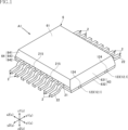
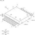
- FIG. 1 is a perspective view showing a semiconductor device according to a first embodiment of the present disclosure.
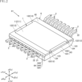
- FIG. 2 is a perspective view showing the semiconductor device according to the first embodiment of the present disclosure.
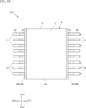
- FIG. 3 is a plan view showing the semiconductor device according to the first embodiment of the present disclosure.
- FIG. 4 is a front view showing the semiconductor device according to the first embodiment of the present disclosure.
- FIG. 5 is a side view showing the semiconductor device according to the first embodiment of the present disclosure.
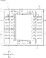
- FIG. 6 is a bottom view showing the semiconductor device according to the first embodiment of the present disclosure.
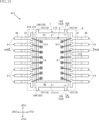
- FIG. 7 is a plan view corresponding to FIG. 3 and seen through the sealing resin.
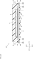
- FIG. 8 is a cross-sectional view taken along line VIII-VIII in FIG. FIG.
- FIG. 9 is a cross-sectional view taken along line IX-IX in FIG.
- FIG. 10 is a plan view of a main portion showing an example of a lead frame used in the method for manufacturing a semiconductor device according to the first embodiment of the present disclosure.
- FIG. 11 is a perspective view for explaining a mold used in the manufacturing method of the semiconductor device according to the first embodiment of the present disclosure.
- FIG. 12 is a front view for explaining a mold used in the method for manufacturing a semiconductor device according to the first embodiment of the present disclosure.
- FIG. 13 is a perspective view showing a semiconductor device according to a first modification of the first embodiment.
- FIG. 14 is a perspective view showing a semiconductor device according to a first modification of the first embodiment.
- FIG. 15 is a plan view showing a semiconductor device according to a first modification of the first embodiment, seen through a sealing resin.
- FIG. 16 is a cross-sectional view taken along line XVI-XVI in FIG.
- FIG. 17 is a cross-sectional view taken along line XVII-XVII in FIG.
- FIG. 18 is a perspective view showing a semiconductor device according to a second modification of the first embodiment.
- FIG. 19 is a plan view showing a semiconductor device according to a second modification of the first embodiment.
- FIG. 20 is a front view showing a semiconductor device according to a second modification of the first embodiment.
- FIG. 21 is a side view showing a semiconductor device according to a second modification of the first embodiment.
- FIG. 22 is a plan view corresponding to FIG.
- FIG. 23 is a cross-sectional view taken along line XXIII-XXIII in FIG.
- FIG. 24 is a plan view showing a semiconductor device according to a third modification of the first embodiment, seen through a sealing resin.
- FIG. 25 is a cross-sectional view taken along line XXV-XXV in FIG.
- FIG. 26 is a cross-sectional view taken along line XXVI-XXVI in FIG.
- an object A is formed on an object B" and “an object A is formed on an object B” include “an object A is formed directly on an object B” and “an object A is formed on an object B with another object interposed between the object A and the object B” unless otherwise specified.
- an object A is disposed on an object B” and “an object A is disposed on an object B” include “an object A is disposed directly on an object B” and “an object A is disposed on an object B with another object interposed between the object A and the object B" unless otherwise specified.
- an object A is located on an object B includes “an object A is located on an object B in contact with an object B” and “an object A is located on an object B with another object interposed between the object A and the object B” unless otherwise specified.
- an object A overlaps an object B when viewed in a certain direction includes “an object A overlaps the entire object B” and “an object A overlaps a part of an object B.”
- a surface A faces (one side or the other side of) direction B” is not limited to the case where the angle of surface A with respect to direction B is 90 degrees, but also includes the case where surface A is tilted with respect to direction B.
- First embodiment: 1 to 9 show a semiconductor device according to a first embodiment of the present disclosure.
- the semiconductor device A1 of this embodiment includes a first lead 1, a plurality of second leads 2, a semiconductor element 3, a plurality of wires 4, and a sealing resin 6.
- the package format of the semiconductor device A1 is a small outline package (SOP).
- SOP small outline package
- the package format of the semiconductor device A1 is not limited to the SOP.
- FIG. 1 is a perspective view showing the semiconductor device A1.
- FIG. 2 is a perspective view showing the semiconductor device A1, showing the semiconductor device A1 turned upside down.
- FIG. 3 is a plan view showing the semiconductor device A1.
- FIG. 4 is a front view showing the semiconductor device A1.
- FIG. 5 is a side view showing the semiconductor device A1.
- FIG. 6 is a bottom view showing the semiconductor device A1.
- FIG. 7 is a plan view showing the semiconductor device A1, showing the sealing resin 6 through it.
- FIG. 8 is a cross-sectional view taken along line VIII-VIII in FIG. 7.
- FIG. 9 is a cross-sectional view taken along line IX-IX in FIG. 7. In FIG. 7, the sealing resin 6 through it is shown by an imaginary line (two-dot chain line).
- the thickness direction of the semiconductor element 3 is referred to as the "thickness direction z.”
- One direction perpendicular to the thickness direction z (the up-down direction in FIG. 3) is referred to as the "first direction x.”
- the direction perpendicular to both the thickness direction z and the first direction x (the left-right direction in FIG. 3) is referred to as the "second direction y.”
- semiconductor device A1 is rectangular (or approximately rectangular) when viewed in the thickness direction z (in a plan view).
- the first lead 1 is a member that supports the semiconductor element 3, and is formed, for example, by cutting and bending a metal plate material such as copper (Cu) or a copper alloy. As shown in Figures 1, 2, 4, and 6 to 9, the first lead 1 of this embodiment has a first portion 11 and four second portions 12.
- the thickness of the first lead 1 is not particularly limited, and is, for example, 0.1 mm to 0.5 mm, with an example of a specific dimension being approximately 0.15 mm.
- the first portion 11 is a portion on which the semiconductor element 3 is mounted. There are no limitations on the shape of the first portion 11, and in the illustrated example, it is rectangular.
- the first portion 11 has a first main surface 111 and a first back surface 112.
- the first main surface 111 is a surface facing the z1 side in the thickness direction z.
- the first main surface 111 is covered with the sealing resin 6.
- the first back surface 112 is a surface facing the z2 side in the thickness direction z.
- the first back surface 112 is exposed from the sealing resin 6.
- an example of the length of one side is approximately 1.5 mm to 5.0 mm.
- the four second parts 12 are located on both outer sides of the first part 11 in the first direction x (the x1 side of the first direction x and the x2 side of the first direction x). Specifically, of the four second parts 12, two second parts 12 are located on the x1 side of the first direction x of the first part 11, and the other two second parts 12 are located on the x2 side of the first direction x of the first part 11. Each of the four second parts 12 is connected to the first part 11.
- the two second parts 12 located on the x1 side of the first direction x of the first part 11 are spaced apart from each other in the second direction y, and are respectively connected to the vicinity of both ends of the first part 11 in the second direction y.
- the two second parts 12 located on the x2 side of the first direction x of the first part 11 are spaced apart from each other in the second direction y, and are respectively connected to the vicinity of both ends of the first part 11 in the second direction y.
- the shape of the second portion 12 is not limited in any way, and in the illustrated example, the dimension (width) in the second direction y is constant (or approximately constant).
- the dimension of the second portion 12 in the second direction y is not limited in any way, and is, for example, about 0.2 mm.
- the second portion 12 has a second main surface 121, a second back surface 122, and a first end surface 123.
- the second main surface 121 faces the z1 side in the thickness direction z.
- the second main surface 121 is covered with sealing resin 6.
- the second back surface 122 faces the z2 side in the thickness direction z.
- the second back surface 122 is exposed from the sealing resin 6.
- the first end surface 123 faces outward in the first direction x.
- the first end surface 123 is connected to the second main surface 121 and the second back surface 122, and is exposed from the sealing resin 6 (the first resin side surface 63 described below).
- the second portion 12 is located at the same position as the first portion 11 in the thickness direction z. More specifically, the second main surface 121 is located at the same position as the first main surface 111 of the first portion 11 in the thickness direction z, and is continuously connected to the first main surface 111. The second back surface 122 is located at the same position as the first back surface 112 of the first portion 11 in the thickness direction z, and is continuously connected to the first back surface 112.
- the first lead 1 may have, for example, two second portions 12.
- one second portion 12 is located on the x1 side of the first portion 11 in the first direction x
- the other second portion 12 is located on the x2 side of the first portion 11 in the first direction x.
- each of the two second portions 12 is connected to the center of the first portion 11 in the second direction y.
- the second leads 2 are used as terminals for mounting the semiconductor device A1 on a wiring board or the like, and are electrically connected to the semiconductor element 3.
- the second leads 2 are formed, for example, by cutting and bending a metal plate material such as copper or a copper alloy. As shown in Figs. 1 to 9, the second leads 2 are spaced apart from the first portion 11 in the second direction y.
- the second leads 2 are arranged on both sides of the first portion 11 (first lead 1) in the second direction y (the y1 side of the second direction y and the y2 side of the second direction y).
- the second leads 2 are arranged at intervals in the first direction x, and in this embodiment, they are arranged at equal intervals along the first direction x.
- the second lead 2 in this embodiment has a lead portion 21 and a terminal portion 22.
- the thickness of the second lead 2 is not particularly limited, and is, for example, 0.1 mm to 0.5 mm, and an example of a specific dimension is about 0.15 mm.
- the lead portion 21 is located on the z1 side of the first portion 11 in the thickness direction z.
- the lead portion 21 has a third main surface 211 and a third back surface 212.
- the third main surface 211 is a surface facing the z1 side of the thickness direction z.
- the third back surface 212 is a surface facing the z2 side of the thickness direction z.
- the third main surface 211 is located on the z1 side of the thickness direction z of the first main surface 111 and the second main surface 121 in the thickness direction z.
- the third back surface 212 is located on the z1 side of the thickness direction z of the first back surface 112 in the thickness direction z.
- the lead portion 21 has a pad portion 213 and a band portion 214.
- the pad portion 213 is the portion to which the wire 4 is bonded.
- the band portion 214 is connected to the pad portion 213 on the side opposite to the first portion 11 in the second direction y.
- the dimension of the pad portion 213 in the first direction x is larger than the dimension of the band portion 214 in the first direction x.
- An example of the dimension of the band portion 214 in the first direction x is about 0.2 mm.
- a part of the band portion 214 and the pad portion 213 are covered with the sealing resin 6, and the other part of the band portion 214 is exposed from the sealing resin 6 (the second resin side surface 64 described below).
- the terminal portion 22 is connected to the end of the lead portion 21 that is farthest from the first portion 11 in the second direction y, and is located outside the lead portion 21 in the second direction y.
- the terminal portion 22 is rectangular with the second direction y as the longitudinal direction.
- the terminal portion 22 is bent in a gull-wing shape when viewed in the first direction x.
- the terminal portion 22 is located on the z2 side of the lead portion 21 in the thickness direction z in the thickness direction z.
- the tip portion of the terminal portion 22 is a portion that is joined to a wiring board or the like when mounted on the wiring board or the like.
- An example of the dimension of the terminal portion 22 in the first direction x is, for example, about 0.2 mm.
- the first lead 1 and the multiple second leads 2 described above are formed from a lead frame LF (see Fig. 10) described later.
- the semiconductor element 3 is an element that performs the main electrical function in the semiconductor device A1.
- the semiconductor element 3 includes an LSI (Large Scale Integration) and an IC (Integrated Circuit).
- the semiconductor element 3 has an element main surface 31 and an element back surface 32.
- the element main surface 31 is a surface facing the z1 side in the thickness direction z.
- the element back surface 32 is a surface facing the z2 side in the thickness direction z.
- a plurality of electrode pads 311 are provided on the element principal surface 31.
- the plurality of electrode pads 311 are arranged, for example, in two rows on the element principal surface 31 along the first direction x.
- the element rear surface 32 faces the first principal surface 111 of the first portion 11 and is joined to the first principal surface 111 by a joining material 39.
- the joining material 39 may be a conductive joining material such as solder or silver (Ag) paste, or an insulating joining material such as an epoxy adhesive.
- the multiple wires 4 provide electrical continuity between the semiconductor element 3 and the multiple second leads 2. As shown in FIG. 7, the multiple wires 4 are individually bonded to the multiple electrode pads 311 of the semiconductor element 3 and the pad portions 213 of the lead portions 21 of the multiple second leads 2.
- the wires 4 are made of, for example, gold (Au), aluminum (Al), copper, etc., and are made of gold in this embodiment.
- the sealing resin 6 covers a portion of the first lead 1, a portion of each of the second leads 2, the semiconductor element 3, and the wires 4.
- the sealing resin 6 is made of an insulating resin, such as a black epoxy resin containing a filler.
- the sealing resin 6 of this embodiment has a resin main surface 61, a resin back surface 62, two first resin side surfaces 63, and two second resin side surfaces 64.
- the resin main surface 61 is a surface facing the z1 side in the thickness direction z.
- the resin back surface 62 is a surface facing the z2 side in the thickness direction z.
- the resin main surface 61 is rectangular.
- the first back surface 112 of the first portion 11 and the second back surfaces 122 of each of the four second portions 12 are exposed from the resin back surface 62.
- the outer edge of the resin back surface 62 is rectangular, and the area ratio of the first back surface 112 to the area enclosed by the outer edge of the resin back surface 62 is, for example, 60% or more and 85% or less.
- each second resin side surface 64 is located between the resin main surface 61 and the resin back surface 62, and are located on both sides in the second direction y (the y1 side of the second direction y and the y2 side of the second direction y).
- each second resin side surface 64 has a first region 641, a second region 642, and a third region 643.
- the first region 641 is connected to the resin main surface 61 and is a region located between the resin main surface 61 and the third main surface 211 of the lead portion 21 in the thickness direction z.
- the first region 641 is inclined with respect to the thickness direction z.
- the second region 642 is connected to the resin back surface 62 and is a region located between the third back surface 212 and the resin back surface 62 in the thickness direction z.
- the second region 642 is inclined with respect to the thickness direction z.
- the third region 643 is a region located between the first region 641 and the second region 642 in the thickness direction z.
- the third region 643 is also located between the third main surface 211 and the third back surface 212 in the thickness direction z, and a part of each of the multiple lead portions 21 (a part of each of the multiple second leads 2) protrudes from this third region 643.
- the lead portion 21 (second lead 2) has a second edge 215.
- the second edge 215 is an edge on the z1 side in the thickness direction z at a portion of the lead portion 21 (second lead 2) that intersects with the second resin side surface 64.
- the second edge 215 is in the same position as the third main surface 211 in the thickness direction z.
- the two first resin side surfaces 63 are located between the resin main surface 61 and the resin back surface 62, and are located on both sides in the first direction x (the x1 side of the first direction x and the x2 side of the first direction x).
- Each first resin side surface 63 in this embodiment has a fourth region 631 and a fifth region 632.
- the fourth region 631 is connected to the resin main surface 61 and is a region located between the resin main surface 61 and the second main surface 121 of the second part 12 in the thickness direction z.
- the fourth region 631 is inclined with respect to the thickness direction z.
- the fifth region 632 is connected to the fourth region 631 on the z2 side in the thickness direction z, and is located between the fourth region 631 and the resin back surface 62 in the thickness direction z.
- the fifth region 632 is located between the second main surface 121 and the second back surface 122 in the thickness direction z, and each first end surface 123 is exposed from this fifth region 632.
- the fifth region 632 is located on the z2 side of the thickness direction z relative to the third region 643 in the thickness direction z.
- the first end surface 123 has a first edge 124.
- the first edge 124 is an edge on the z1 side of the first end surface 123 in the thickness direction z.
- the first edge 124 is in the same position as the second main surface 121 in the thickness direction z.
- the third main surface 211 is located on the z1 side in the thickness direction z relative to the first main surface 111 and the second main surface 121.
- the first edge 124 which is located at the same position as the second main surface 121 in the thickness direction z, is located on the z2 side in the thickness direction z relative to the second edge 215, which is located at the same position as the third main surface 211 in the thickness direction z.
- the lead frame LF shows a lead frame LF, which is an example of a component used in manufacturing the semiconductor device A1.
- the lead frame LF includes a frame F, a lead 10 connected to the frame F, a number of leads 20, and a tie bar 210.
- Most of the lead 10 and most of the leads 20 are portions that become the first lead 1 and the second leads 2 when cut from the lead frame LF.
- the lead 10 has a first portion 11, four second portions 120, and four bent portions 130.
- the second portion 120 is a portion that becomes the second portion 12.
- the lead frame LF has a portion that connects the frame F and the second portion 120 by depression processing so that the first portion 11 and the second portion 120 are located on the z2 side of the frame F in the thickness direction z.
- the bent portion 130 is a portion that is deformed by depression processing. When the lead frame LF is cut, it is cut along the boundary between the second portion 120 and the bent portion 130. Of the lead frame LF, the frame F, the bent portion 130, and the tie bar 210 do not constitute the semiconductor device A1.
- the first main surface 111 of the first portion 11 and the pad portion 213 may be provided with a plating layer made of silver, nickel (Ni), or the like, as necessary. After mounting the semiconductor element 3 and bonding the multiple wires 4 to the lead frame LF, the sealing resin 6 is formed.
- the sealing resin 6 is formed, for example, by transfer molding.
- Figures 11 and 12 show an example of the schematic configuration of a mold used to form the sealing resin 6.
- the lead frame LF is housed in a mold 8 having multiple cavities.
- the mold 8 includes, for example, a lower mold 81 having a cavity 810 and an upper mold 82 having a cavity 820, and the portions of the lead frame LF that are covered with the sealing resin 6 in the semiconductor device A1 (lead 10 and parts of the multiple leads 20) are housed in the cavities 810, 820.
- the lower mold 81 has a mating surface 811 and a mating surface 812.
- the mating surface 811 is located at a position corresponding to the first resin side surface 63 of the sealing resin 6, and the mating surface 812 is located at a position corresponding to the second resin side surface 64.
- the mating surface 811 corresponding to the first resin side surface 63 and the mating surface 812 corresponding to the second resin side surface 64 are located at different positions in the thickness direction z.
- the mating surface 811 is located on the z2 side of the mating surface 812 in the thickness direction z.
- the upper mold 82 has a mating surface 821 and a mating surface 822.
- the mating surface 821 is located at a position corresponding to the first resin side surface 63, and the mating surface 822 is located at a position corresponding to the second resin side surface 64.
- the mating surface 821 corresponding to the first resin side surface 63 and the mating surface 822 corresponding to the second resin side surface 64 are located at different positions in the thickness direction z.
- the mating surface 821 is located on the z2 side of the mating surface 822 in the thickness direction z.
- each second portion 120 is sandwiched between the mating surface 811 of the lower mold 81 and the mating surface 821 of the upper mold 82, and each lead 20 is sandwiched between the mating surface 821 of the lower mold 81 and the mating surface 822 of the upper mold 82.
- fluidized resin is poured into the cavities 810, 820 of the mold 8 to fill them, and the resin is then solidified. After that, punching or other processes are performed to separate the lead 10 and multiple leads 20 (the portions that will become the first lead 1 and multiple second leads 2) that were connected to each other by the frame F and tie bars 210 are appropriately separated. Next, bending is performed on the portions of the multiple second leads 2 that protrude from the sealing resin 6. Through the processes described above, the semiconductor device A1 is manufactured.
- the first lead 1 has a first end surface 123 located on both sides in the first direction x and exposed from the first resin side surface 63.
- the first end surface 123 has a first edge 124 located on the z1 side of the thickness direction z.
- the second leads 2 protrude from the two second resin side surfaces 64 to both sides in the second direction y.
- the second lead 2 has a second edge 215 located on the z1 side of the thickness direction z at a portion intersecting with the second resin side surface 64.
- the first edge 124 of the first lead 1 is located on the z2 side of the thickness direction z relative to the second edge 215 in the thickness direction z.
- the first lead 1 on which the semiconductor element 3 is mounted does not have a bent portion deformed in the thickness direction z by the depression process. Therefore, it is possible to eliminate the inconvenience of having a bent portion due to the depression process in the lead and to relatively increase the size of the portion (first portion 11) on which the semiconductor element 3 is mounted.
- the first lead 1 includes a first portion 11 on which a semiconductor element 3 is mounted, and second portions 12 each connected to the first portion 11 and located on both outer sides of the first portion 11 in the first direction x.
- the second portions 12 have a first end surface 123.
- the first portion 11 has a first main surface 111 facing the z1 side in the thickness direction z, and a first back surface 112 facing the z2 side in the thickness direction z, and the semiconductor element 3 is supported by the first main surface 111.
- the first back surface 112 is exposed from the resin back surface 62.
- the second portion 12 has a second main surface 121 facing the z1 side in the thickness direction z, and a second back surface 122 facing the z2 side in the thickness direction z.
- the second main surface 121 is located at the same position as the first main surface 111 of the first portion 11 in the thickness direction z.
- the second back surface 122 is located at the same position as the first back surface 112 of the first portion 11 in the thickness direction z, and is exposed from the resin back surface 62. With this configuration, it is possible to easily form the first portion 11 and the second portion 12 connected thereto. Furthermore, since the second back surface 122 is exposed from the resin back surface 62 in addition to the first back surface 112, it is possible to further improve the heat dissipation properties of the semiconductor device A1.
- the second resin side surface 64 has a first region 641, a second region 642, and a third region 643.
- the first region 641 is connected to the resin main surface 61, and the second region 642 is connected to the resin back surface 62.
- the third region 643 is located between the first region 641 and the second region 642 in the thickness direction z. A part of each of the multiple second leads 2 protrudes from this third region 643.
- the first resin side surface 63 has a fourth region 631 and a fifth region 632.
- the fourth region 631 is connected to the resin main surface 61, and the fifth region 632 is connected to the z2 side of the fourth region 631 in the thickness direction z and is connected to the resin back surface 62.
- the fifth region 632 is located on the z2 side of the third region 643 in the thickness direction z.
- the first end face 123 is exposed from this fifth region 632.
- the semiconductor device A1 having the sealing resin 6 configured in this way can be manufactured by forming the sealing resin 6 by the transfer molding process described above.
- FIG. 13 to 17 show a semiconductor device according to a first modification of the first embodiment.
- FIG. 13 is a perspective view of the semiconductor device A11 of this modification.
- FIG. 14 is a perspective view of the semiconductor device A11, showing the semiconductor device A11 turned upside down.
- FIG. 15 is a plan view of the semiconductor device A11, showing the sealing resin 6 through the semiconductor device A11.
- FIG. 16 is a cross-sectional view taken along line XVI-XVI in FIG. 15.
- FIG. 17 is a cross-sectional view taken along line XVII-XVII in FIG. 15.
- the sealing resin 6 through the sealing resin 6 is shown by an imaginary line (two-dot chain line).
- elements that are the same as or similar to those of the semiconductor device A1 of the above embodiment are given the same reference numerals as those of the above embodiment, and descriptions thereof will be omitted as appropriate.
- the configuration of the first portion 11 and the second portion 12 is different from that of the semiconductor device A1 of the above embodiment.
- the first portion 11 has a back side recess 113.
- the back side recess 113 is recessed from the first back side 112 to the z1 side in the thickness direction z at the outer periphery of the first portion 11 as viewed in the thickness direction z.
- This back side recess 113 is covered with sealing resin 6.
- the second back side 122 of the second portion 12 is located on the z1 side in the thickness direction z relative to the first back side 112 in the thickness direction z.
- the second back side 122 is covered with sealing resin 6.
- the back side recess 113 and the second back side 122 of the above configuration are formed, for example, by half-etching the back side of the first lead 1.
- the first lead 1 has a first end surface 123 located on both sides in the first direction x and exposed from the first resin side surface 63.
- the first end surface 123 has a first edge 124 located on the z1 side of the thickness direction z.
- the second leads 2 protrude from the two second resin side surfaces 64 to both sides in the second direction y.
- the second lead 2 has a second edge 215 located on the z1 side of the thickness direction z at a portion intersecting with the second resin side surface 64.
- the first edge 124 of the first lead 1 is located on the z2 side of the thickness direction z relative to the second edge 215 in the thickness direction z.
- the first lead 1 on which the semiconductor element 3 is mounted does not have a bent portion deformed in the thickness direction z by the depression process. Therefore, it is possible to eliminate the inconvenience of having a bent portion due to the depression process in the lead and to relatively increase the size of the portion (first portion 11) on which the semiconductor element 3 is mounted.
- the first portion 11 has a back side recess 113.
- the back side recess 113 is recessed from the first back surface 112 to the z1 side in the thickness direction z at the outer periphery of the first portion 11 as viewed in the thickness direction z, and is covered with the sealing resin 6.
- the second back surface 122 of the second portion 12 is located on the z1 side in the thickness direction z relative to the first back surface 112 in the thickness direction z, and is covered with the sealing resin 6.
- FIG. 18 to 23 show a semiconductor device according to a second modified example of the first embodiment.
- FIG. 18 is a perspective view showing a semiconductor device A12 of this modified example.
- FIG. 19 is a plan view showing the semiconductor device A12.
- FIG. 20 is a front view showing the semiconductor device A12.
- FIG. 21 is a side view showing the semiconductor device A12.
- FIG. 22 is a plan view corresponding to FIG. 19, showing through the sealing resin 6.
- FIG. 23 is a cross-sectional view taken along line XXIII-XXIII in FIG. 22. In FIG. 22, the sealing resin 6 shown through is shown by an imaginary line (two-dot chain line).
- the main difference between the semiconductor device A1 of the above embodiment is the configuration of the two first resin side surfaces 63 in the sealing resin 6.
- the first resin side surfaces 63 are shaped entirely along a plane perpendicular to the first direction x.
- the first resin side surfaces 63 of this configuration are formed by cutting with a blade after the sealing resin 6 is formed during the manufacturing process of the semiconductor device A12.
- the first lead 1 has a first end surface 123 located on both sides in the first direction x and exposed from the first resin side surface 63.
- the first end surface 123 has a first edge 124 located on the z1 side of the thickness direction z.
- the multiple second leads 2 protrude from the two second resin side surfaces 64 to both sides in the second direction y.
- the second lead 2 has a second edge 215 located on the z1 side of the thickness direction z at the portion intersecting with the second resin side surface 64.
- the first edge 124 of the first lead 1 is located on the z2 side of the thickness direction z relative to the second edge 215 in the thickness direction z.
- the semiconductor device A12 has the same effects as the semiconductor device A1 within the same range of configuration as the semiconductor device A1 of the above embodiment.
- Figures 24 to 26 show a semiconductor device according to a third modified example of the first embodiment.
- Figure 24 is a plan view showing a semiconductor device A13 of this modified example, seen through the sealing resin 6.
- Figure 25 is a cross-sectional view taken along line XXV-XXV in Figure 24.
- Figure 26 is a cross-sectional view taken along line XXVI-XXVI in Figure 24.
- the seen-through sealing resin 6 is shown by an imaginary line (two-dot chain line).
- the configuration of the second part 12 is mainly different from that of the semiconductor device A1 of the above embodiment.
- the second part 12 has a bent part 125 and an end part 126.
- the end part 126 has a first end face 123.
- the surface of the end part 126 facing the z2 side in the thickness direction z is exposed from the resin back surface 62.
- the bent part 125 is interposed between the end part 126 and the first part 11, and is inclined so as to be located on the z1 side in the thickness direction z as it approaches the first part 11.
- the bent part 125 and the end part 126 of this configuration are formed, for example, by performing a bending process on the second part 12 (first lead 1).
- the first back surface 112 of the first part 11 is located on the z1 side in the thickness direction z from the resin back surface 62, and is covered with the sealing resin 6.
- the first lead 1 has a first end surface 123 located on both sides in the first direction x and exposed from the first resin side surface 63.
- the first end surface 123 has a first edge 124 located on the z1 side of the thickness direction z.
- the multiple second leads 2 protrude from the two second resin side surfaces 64 to both sides in the second direction y.
- the second lead 2 has a second edge 215 located on the z1 side of the thickness direction z at the portion intersecting with the second resin side surface 64.
- the first edge 124 of the first lead 1 is located on the z2 side of the thickness direction z relative to the second edge 215 in the thickness direction z.
- the semiconductor device A13 has the same effects as the semiconductor device A1 within the same range of configuration as the semiconductor device A1 of the above embodiment.
- the semiconductor device according to the present disclosure is not limited to the above-mentioned embodiment.
- the specific configuration of each part of the semiconductor device according to the present disclosure can be freely designed in various ways.
- the package format of the semiconductor device is SOP, and the portions of the multiple second leads 2 exposed from the sealing resin 6 are bent in a gull-wing shape, but the present disclosure is not limited to this.
- the semiconductor device of the present disclosure can be applied to, for example, a DIP (Dual In-line Package) package format in which the second leads 2 exposed from the sealing resin 6 are bent and extend toward the z2 side in the thickness direction z, or a SOJ (Small Outline J-leaded Package) package format in which the second leads 2 exposed from the sealing resin 6 are bent in a J shape.
- Appendix 1 A semiconductor element; a first lead on which the semiconductor element is mounted; a plurality of second leads spaced apart from the first leads; a sealing resin that covers the semiconductor element, the first lead, and the second leads; the semiconductor element is disposed on one side of the first lead in a thickness direction, the sealing resin has a resin main surface facing one side in the thickness direction, a resin back surface facing the other side in the thickness direction, two first resin side surfaces located between the resin main surface and the resin back surface and spaced apart in a first direction perpendicular to the thickness direction, and two second resin side surfaces located between the resin main surface and the resin back surface and spaced apart in a second direction perpendicular to the thickness direction and the first direction, the first lead has a first end surface exposed from one of the two first resin side surfaces; the plurality of second leads include at least one second lead protruding in the second direction from one of the two second resin side surfaces; The first end surface has a first edge located on one side
- the first lead includes a first portion; The first portion has a first main surface facing one side in the thickness direction and a first back surface facing the other side in the thickness direction, 2.
- the semiconductor device according to claim 1 wherein the semiconductor element is supported by the first main surface.
- Appendix 3. 3.
- Appendix 4. the first lead includes a second portion connected to the first portion; The semiconductor device according to claim 2 or 3, wherein the second portion has the first end surface.
- the second portion has a second main surface facing one side in the thickness direction and a second back surface facing the other side in the thickness direction, 5.
- the first portion has an outer periphery when viewed in the thickness direction, and the outer periphery has a back surface side recess that is recessed from the first back surface to one side in the thickness direction.
- Appendix 11. the at least one second lead includes a lead portion that is partially covered with the sealing resin and extends along the second direction; 11. The semiconductor device according to claim 2, wherein the lead portion has the second edge.
- Appendix 12. the lead portion has a third main surface facing one side in the thickness direction and a third back surface facing the other side in the thickness direction, 12. The semiconductor device according to claim 11, wherein the third main surface is located on one side in the thickness direction with respect to the first main surface.
- the semiconductor element has an element main surface facing one side in the thickness direction and an element back surface facing the other side in the thickness direction and facing the first main surface; 13.
- Appendix 14. the at least one second lead includes a terminal portion connected to the lead portion; 14.
- Appendix 15. the one second resin side surface has a first region connected to the resin main surface, a second region connected to the resin back surface, and a third region located between the first region and the second region in the thickness direction, 15.
- Appendix 16. the first resin side surface has a fourth region connected to the resin main surface and a fifth region connected to the other side in the thickness direction of the fourth region, the fifth region is located on the other side in the thickness direction with respect to the third region, 16.
- Appendix 17. 16.
- the semiconductor device according to claim 15, wherein the two first resin side surfaces are each flat surfaces perpendicular to the first direction.
Landscapes
- Structures Or Materials For Encapsulating Or Coating Semiconductor Devices Or Solid State Devices (AREA)
- Engineering & Computer Science (AREA)
- Microelectronics & Electronic Packaging (AREA)
Priority Applications (2)
| Application Number | Priority Date | Filing Date | Title |
|---|---|---|---|
| JP2024576317A JPWO2024166846A1 (https=) | 2023-02-08 | 2024-02-05 | |
| US19/288,125 US20250357283A1 (en) | 2023-02-08 | 2025-08-01 | Semiconductor device |
Applications Claiming Priority (2)
| Application Number | Priority Date | Filing Date | Title |
|---|---|---|---|
| JP2023-017617 | 2023-02-08 | ||
| JP2023017617 | 2023-02-08 |
Related Child Applications (1)
| Application Number | Title | Priority Date | Filing Date |
|---|---|---|---|
| US19/288,125 Continuation US20250357283A1 (en) | 2023-02-08 | 2025-08-01 | Semiconductor device |
Publications (1)
| Publication Number | Publication Date |
|---|---|
| WO2024166846A1 true WO2024166846A1 (ja) | 2024-08-15 |
Family
ID=92262582
Family Applications (1)
| Application Number | Title | Priority Date | Filing Date |
|---|---|---|---|
| PCT/JP2024/003633 Ceased WO2024166846A1 (ja) | 2023-02-08 | 2024-02-05 | 半導体装置 |
Country Status (3)
| Country | Link |
|---|---|
| US (1) | US20250357283A1 (https=) |
| JP (1) | JPWO2024166846A1 (https=) |
| WO (1) | WO2024166846A1 (https=) |
Citations (3)
| Publication number | Priority date | Publication date | Assignee | Title |
|---|---|---|---|---|
| JPH0233961A (ja) * | 1988-07-23 | 1990-02-05 | Nec Corp | リードフレーム |
| JPH04748A (ja) * | 1990-04-17 | 1992-01-06 | Mitsubishi Electric Corp | リードフレームおよび半導体装置の製造方法 |
| JP2013508974A (ja) * | 2009-10-19 | 2013-03-07 | ナショナル セミコンダクター コーポレーション | 向上した接地ボンド信頼性を有するリードフレーム・パッケージ |
-
2024
- 2024-02-05 WO PCT/JP2024/003633 patent/WO2024166846A1/ja not_active Ceased
- 2024-02-05 JP JP2024576317A patent/JPWO2024166846A1/ja active Pending
-
2025
- 2025-08-01 US US19/288,125 patent/US20250357283A1/en active Pending
Patent Citations (3)
| Publication number | Priority date | Publication date | Assignee | Title |
|---|---|---|---|---|
| JPH0233961A (ja) * | 1988-07-23 | 1990-02-05 | Nec Corp | リードフレーム |
| JPH04748A (ja) * | 1990-04-17 | 1992-01-06 | Mitsubishi Electric Corp | リードフレームおよび半導体装置の製造方法 |
| JP2013508974A (ja) * | 2009-10-19 | 2013-03-07 | ナショナル セミコンダクター コーポレーション | 向上した接地ボンド信頼性を有するリードフレーム・パッケージ |
Also Published As
| Publication number | Publication date |
|---|---|
| US20250357283A1 (en) | 2025-11-20 |
| JPWO2024166846A1 (https=) | 2024-08-15 |
Similar Documents
| Publication | Publication Date | Title |
|---|---|---|
| US8704342B2 (en) | Resin sealing type semiconductor device and method of manufacturing the same, and lead frame | |
| US9741641B2 (en) | Method for manufacturing semiconductor device, and semiconductor device | |
| US9385072B2 (en) | Method of manufacturing semiconductor device and semiconductor device | |
| US9779966B2 (en) | Lead frame and semiconductor device | |
| TWI650840B (zh) | 引線支架、半導體裝置及引線支架之製造方法 | |
| TW200818458A (en) | Stackable packages for three-dimensional packaging of semiconductor dice | |
| JP7089388B2 (ja) | 半導体装置および半導体装置の製造方法 | |
| JP2005057067A (ja) | 半導体装置およびその製造方法 | |
| JP7210868B2 (ja) | 半導体装置 | |
| JP2014232811A (ja) | 半導体装置および半導体装置の製造方法 | |
| US7595549B2 (en) | Surface mount semiconductor device | |
| JP7569912B2 (ja) | 半導体装置 | |
| US7436049B2 (en) | Lead frame, semiconductor chip package using the lead frame, and method of manufacturing the semiconductor chip package | |
| JP2019121698A (ja) | 半導体装置および半導体装置の製造方法 | |
| JP2009064854A (ja) | リードフレーム、半導体装置、及び半導体装置の製造方法 | |
| JP7193284B2 (ja) | リードフレーム及びリードフレームの製造方法 | |
| JPH11145364A (ja) | 樹脂封止型半導体装置及びその製造方法 | |
| WO2022196278A1 (ja) | 半導体装置 | |
| WO2024166846A1 (ja) | 半導体装置 | |
| JP2025144628A (ja) | 半導体装置、および半導体装置の製造方法 | |
| JP7827700B2 (ja) | 半導体装置 | |
| JP2002164496A (ja) | 半導体装置およびその製造方法 | |
| JP2017108191A (ja) | 半導体装置 | |
| JPH0778930A (ja) | 半導体装置およびその外部リード | |
| HK1237992A1 (en) | Semiconductor device manufacturing method and semiconductor device |
Legal Events
| Date | Code | Title | Description |
|---|---|---|---|
| 121 | Ep: the epo has been informed by wipo that ep was designated in this application |
Ref document number: 24753289 Country of ref document: EP Kind code of ref document: A1 |
|
| ENP | Entry into the national phase |
Ref document number: 2024576317 Country of ref document: JP Kind code of ref document: A |
|
| WWE | Wipo information: entry into national phase |
Ref document number: 2024576317 Country of ref document: JP |
|
| NENP | Non-entry into the national phase |
Ref country code: DE |
|
| 122 | Ep: pct application non-entry in european phase |
Ref document number: 24753289 Country of ref document: EP Kind code of ref document: A1 |