WO2024166268A1 - 露光方法、露光装置、及びデバイス製造方法 - Google Patents
露光方法、露光装置、及びデバイス製造方法 Download PDFInfo
- Publication number
- WO2024166268A1 WO2024166268A1 PCT/JP2023/004244 JP2023004244W WO2024166268A1 WO 2024166268 A1 WO2024166268 A1 WO 2024166268A1 JP 2023004244 W JP2023004244 W JP 2023004244W WO 2024166268 A1 WO2024166268 A1 WO 2024166268A1
- Authority
- WO
- WIPO (PCT)
- Prior art keywords
- exposure light
- light
- exposure
- image
- pattern
- Prior art date
- Legal status (The legal status is an assumption and is not a legal conclusion. Google has not performed a legal analysis and makes no representation as to the accuracy of the status listed.)
- Ceased
Links
Images




Classifications
-
- G—PHYSICS
- G03—PHOTOGRAPHY; CINEMATOGRAPHY; ANALOGOUS TECHNIQUES USING WAVES OTHER THAN OPTICAL WAVES; ELECTROGRAPHY; HOLOGRAPHY
- G03F—PHOTOMECHANICAL PRODUCTION OF TEXTURED OR PATTERNED SURFACES, e.g. FOR PRINTING, FOR PROCESSING OF SEMICONDUCTOR DEVICES; MATERIALS THEREFOR; ORIGINALS THEREFOR; APPARATUS SPECIALLY ADAPTED THEREFOR
- G03F7/00—Photomechanical, e.g. photolithographic, production of textured or patterned surfaces, e.g. printing surfaces; Materials therefor, e.g. comprising photoresists; Apparatus specially adapted therefor
- G03F7/70—Microphotolithographic exposure; Apparatus therefor
- G03F7/70483—Information management; Active and passive control; Testing; Wafer monitoring, e.g. pattern monitoring
- G03F7/7055—Exposure light control in all parts of the microlithographic apparatus, e.g. pulse length control or light interruption
- G03F7/70558—Dose control, i.e. achievement of a desired dose
-
- G—PHYSICS
- G03—PHOTOGRAPHY; CINEMATOGRAPHY; ANALOGOUS TECHNIQUES USING WAVES OTHER THAN OPTICAL WAVES; ELECTROGRAPHY; HOLOGRAPHY
- G03F—PHOTOMECHANICAL PRODUCTION OF TEXTURED OR PATTERNED SURFACES, e.g. FOR PRINTING, FOR PROCESSING OF SEMICONDUCTOR DEVICES; MATERIALS THEREFOR; ORIGINALS THEREFOR; APPARATUS SPECIALLY ADAPTED THEREFOR
- G03F7/00—Photomechanical, e.g. photolithographic, production of textured or patterned surfaces, e.g. printing surfaces; Materials therefor, e.g. comprising photoresists; Apparatus specially adapted therefor
- G03F7/70—Microphotolithographic exposure; Apparatus therefor
- G03F7/70483—Information management; Active and passive control; Testing; Wafer monitoring, e.g. pattern monitoring
- G03F7/7055—Exposure light control in all parts of the microlithographic apparatus, e.g. pulse length control or light interruption
- G03F7/70575—Wavelength control, e.g. control of bandwidth, multiple wavelength, selection of wavelength or matching of optical components to wavelength
-
- G—PHYSICS
- G03—PHOTOGRAPHY; CINEMATOGRAPHY; ANALOGOUS TECHNIQUES USING WAVES OTHER THAN OPTICAL WAVES; ELECTROGRAPHY; HOLOGRAPHY
- G03F—PHOTOMECHANICAL PRODUCTION OF TEXTURED OR PATTERNED SURFACES, e.g. FOR PRINTING, FOR PROCESSING OF SEMICONDUCTOR DEVICES; MATERIALS THEREFOR; ORIGINALS THEREFOR; APPARATUS SPECIALLY ADAPTED THEREFOR
- G03F7/00—Photomechanical, e.g. photolithographic, production of textured or patterned surfaces, e.g. printing surfaces; Materials therefor, e.g. comprising photoresists; Apparatus specially adapted therefor
- G03F7/20—Exposure; Apparatus therefor
-
- G—PHYSICS
- G03—PHOTOGRAPHY; CINEMATOGRAPHY; ANALOGOUS TECHNIQUES USING WAVES OTHER THAN OPTICAL WAVES; ELECTROGRAPHY; HOLOGRAPHY
- G03F—PHOTOMECHANICAL PRODUCTION OF TEXTURED OR PATTERNED SURFACES, e.g. FOR PRINTING, FOR PROCESSING OF SEMICONDUCTOR DEVICES; MATERIALS THEREFOR; ORIGINALS THEREFOR; APPARATUS SPECIALLY ADAPTED THEREFOR
- G03F7/00—Photomechanical, e.g. photolithographic, production of textured or patterned surfaces, e.g. printing surfaces; Materials therefor, e.g. comprising photoresists; Apparatus specially adapted therefor
- G03F7/70—Microphotolithographic exposure; Apparatus therefor
- G03F7/70008—Production of exposure light, i.e. light sources
- G03F7/70025—Production of exposure light, i.e. light sources by lasers
-
- G—PHYSICS
- G03—PHOTOGRAPHY; CINEMATOGRAPHY; ANALOGOUS TECHNIQUES USING WAVES OTHER THAN OPTICAL WAVES; ELECTROGRAPHY; HOLOGRAPHY
- G03F—PHOTOMECHANICAL PRODUCTION OF TEXTURED OR PATTERNED SURFACES, e.g. FOR PRINTING, FOR PROCESSING OF SEMICONDUCTOR DEVICES; MATERIALS THEREFOR; ORIGINALS THEREFOR; APPARATUS SPECIALLY ADAPTED THEREFOR
- G03F7/00—Photomechanical, e.g. photolithographic, production of textured or patterned surfaces, e.g. printing surfaces; Materials therefor, e.g. comprising photoresists; Apparatus specially adapted therefor
- G03F7/70—Microphotolithographic exposure; Apparatus therefor
- G03F7/70008—Production of exposure light, i.e. light sources
- G03F7/7005—Production of exposure light, i.e. light sources by multiple sources, e.g. light-emitting diodes [LED] or light source arrays
-
- G—PHYSICS
- G03—PHOTOGRAPHY; CINEMATOGRAPHY; ANALOGOUS TECHNIQUES USING WAVES OTHER THAN OPTICAL WAVES; ELECTROGRAPHY; HOLOGRAPHY
- G03F—PHOTOMECHANICAL PRODUCTION OF TEXTURED OR PATTERNED SURFACES, e.g. FOR PRINTING, FOR PROCESSING OF SEMICONDUCTOR DEVICES; MATERIALS THEREFOR; ORIGINALS THEREFOR; APPARATUS SPECIALLY ADAPTED THEREFOR
- G03F7/00—Photomechanical, e.g. photolithographic, production of textured or patterned surfaces, e.g. printing surfaces; Materials therefor, e.g. comprising photoresists; Apparatus specially adapted therefor
- G03F7/70—Microphotolithographic exposure; Apparatus therefor
- G03F7/70058—Mask illumination systems
- G03F7/70208—Multiple illumination paths, e.g. radiation distribution devices, microlens illumination systems, multiplexers or demultiplexers for single or multiple projection systems
-
- G—PHYSICS
- G03—PHOTOGRAPHY; CINEMATOGRAPHY; ANALOGOUS TECHNIQUES USING WAVES OTHER THAN OPTICAL WAVES; ELECTROGRAPHY; HOLOGRAPHY
- G03F—PHOTOMECHANICAL PRODUCTION OF TEXTURED OR PATTERNED SURFACES, e.g. FOR PRINTING, FOR PROCESSING OF SEMICONDUCTOR DEVICES; MATERIALS THEREFOR; ORIGINALS THEREFOR; APPARATUS SPECIALLY ADAPTED THEREFOR
- G03F7/00—Photomechanical, e.g. photolithographic, production of textured or patterned surfaces, e.g. printing surfaces; Materials therefor, e.g. comprising photoresists; Apparatus specially adapted therefor
- G03F7/70—Microphotolithographic exposure; Apparatus therefor
- G03F7/70216—Mask projection systems
- G03F7/70283—Mask effects on the imaging process
- G03F7/70291—Addressable masks, e.g. spatial light modulators [SLMs], digital micro-mirror devices [DMDs] or liquid crystal display [LCD] patterning devices
-
- G—PHYSICS
- G03—PHOTOGRAPHY; CINEMATOGRAPHY; ANALOGOUS TECHNIQUES USING WAVES OTHER THAN OPTICAL WAVES; ELECTROGRAPHY; HOLOGRAPHY
- G03F—PHOTOMECHANICAL PRODUCTION OF TEXTURED OR PATTERNED SURFACES, e.g. FOR PRINTING, FOR PROCESSING OF SEMICONDUCTOR DEVICES; MATERIALS THEREFOR; ORIGINALS THEREFOR; APPARATUS SPECIALLY ADAPTED THEREFOR
- G03F7/00—Photomechanical, e.g. photolithographic, production of textured or patterned surfaces, e.g. printing surfaces; Materials therefor, e.g. comprising photoresists; Apparatus specially adapted therefor
- G03F7/70—Microphotolithographic exposure; Apparatus therefor
- G03F7/70216—Mask projection systems
- G03F7/70308—Optical correction elements, filters or phase plates for manipulating imaging light, e.g. intensity, wavelength, polarisation, phase or image shift
-
- G—PHYSICS
- G03—PHOTOGRAPHY; CINEMATOGRAPHY; ANALOGOUS TECHNIQUES USING WAVES OTHER THAN OPTICAL WAVES; ELECTROGRAPHY; HOLOGRAPHY
- G03F—PHOTOMECHANICAL PRODUCTION OF TEXTURED OR PATTERNED SURFACES, e.g. FOR PRINTING, FOR PROCESSING OF SEMICONDUCTOR DEVICES; MATERIALS THEREFOR; ORIGINALS THEREFOR; APPARATUS SPECIALLY ADAPTED THEREFOR
- G03F7/00—Photomechanical, e.g. photolithographic, production of textured or patterned surfaces, e.g. printing surfaces; Materials therefor, e.g. comprising photoresists; Apparatus specially adapted therefor
- G03F7/70—Microphotolithographic exposure; Apparatus therefor
- G03F7/70216—Mask projection systems
- G03F7/70358—Scanning exposure, i.e. relative movement of patterned beam and workpiece during imaging
-
- G—PHYSICS
- G03—PHOTOGRAPHY; CINEMATOGRAPHY; ANALOGOUS TECHNIQUES USING WAVES OTHER THAN OPTICAL WAVES; ELECTROGRAPHY; HOLOGRAPHY
- G03F—PHOTOMECHANICAL PRODUCTION OF TEXTURED OR PATTERNED SURFACES, e.g. FOR PRINTING, FOR PROCESSING OF SEMICONDUCTOR DEVICES; MATERIALS THEREFOR; ORIGINALS THEREFOR; APPARATUS SPECIALLY ADAPTED THEREFOR
- G03F7/00—Photomechanical, e.g. photolithographic, production of textured or patterned surfaces, e.g. printing surfaces; Materials therefor, e.g. comprising photoresists; Apparatus specially adapted therefor
- G03F7/70—Microphotolithographic exposure; Apparatus therefor
- G03F7/70483—Information management; Active and passive control; Testing; Wafer monitoring, e.g. pattern monitoring
- G03F7/70491—Information management, e.g. software; Active and passive control, e.g. details of controlling exposure processes or exposure tool monitoring processes
- G03F7/70525—Controlling normal operating mode, e.g. matching different apparatus, remote control or prediction of failure
Definitions
- a pattern with a large depth compared to its width (high aspect ratio), so-called grooves may be exposed onto a photosensitive material layer on a substrate (glass plate or semiconductor wafer, etc.) (for example, Patent Document 1).
- an exposure method including illuminating a first object with exposure light including a first exposure light of a first wavelength and a second exposure light of a second wavelength different from the first wavelength, and exposing an image of a pattern of the first object onto a second object with the exposure light from the first object, wherein the exposing includes forming a first image of the pattern of the first object with the first exposure light from the first object, and forming a second image of the pattern of the first object with the second exposure light from the first object at a position farther from the surface of the second object than the first image in the traveling direction of the second exposure light, and the intensity of the second exposure light irradiated to the second object is higher than the intensity of the first exposure light irradiated to the second object.
- an exposure method including illuminating a first object with exposure light including a first exposure light of a first wavelength and a second exposure light of a second wavelength different from the first wavelength, and exposing a second object moving along a scanning direction with the exposure light from the first object, wherein the exposing includes forming a first image of a pattern of the first object with the first exposure light from the first object, and forming a second image of the pattern of the first object with the second exposure light from the first object at a position farther from the surface of the second object than the first image in the traveling direction of the second exposure light, and the timing at which the second exposure light is irradiated to the second object is different from the timing at which the first exposure light is irradiated to the second object.
- an exposure apparatus including an illumination optical system that illuminates a first object with exposure light including a first exposure light of a first wavelength and a second exposure light of a second wavelength different from the first wavelength, and a projection optical system that projects an image of a pattern of the first object onto a second object with the exposure light from the first object, wherein the projection optical system forms a first image of the pattern of the first object with the first exposure light from the first object, and forms a second image of the pattern of the first object with the second exposure light from the first object at a position farther from the surface of the second object than the first image in the traveling direction of the second exposure light, and the intensity of the second exposure light irradiated to the second object is higher than the intensity of the first exposure light irradiated to the second object.
- an exposure apparatus that scans and exposes a pattern of a first object onto a second object
- the exposure apparatus comprising: an illumination optical system that illuminates the first object with exposure light including a first exposure light of a first wavelength and a second exposure light of a second wavelength different from the first wavelength; a projection optical system that projects the exposure light from the first object onto a second object moving along a scanning direction; and a control device that controls a light source that supplies the exposure light to the illumination optical system, the projection optical system forming a first image of the pattern of the first object with the first exposure light from the first object, and forming a second image of the pattern of the first object with the second exposure light from the first object at a position farther from the surface of the second object than the first image in the traveling direction of the second exposure light, and the control device controlling the timing at which the second exposure light is irradiated onto the second object to be different from the timing at which the first exposure light is irradiated onto the second object.
- a device manufacturing method includes exposing a photosensitive material layer of the second object using the above-described exposure method, and processing an area inside the photosensitive material layer of the second object using a pattern generated by developing the exposed photosensitive material layer as a mask.
- FIG. 1 is a diagram showing a schematic configuration of an exposure apparatus according to an embodiment.
- FIG. 2A is a diagram showing a schematic configuration of a light source unit
- FIG. 2B is a diagram showing examples of wavelengths of light emitted from each solid-state laser light source.
- FIG. 3 is a diagram showing an example of a spatial light modulator.
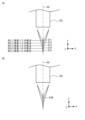
- FIG. 4 is a diagram for explaining the longitudinal chromatic aberration.
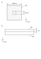
- FIG. 5A is a schematic diagram showing a mask used in the simulation
- FIG. 5B is a schematic diagram showing a substrate and a resist used in the simulation.
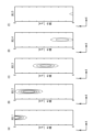
- FIGS. 6A to 6E are diagrams showing the results of simulating the intensity distribution of a pattern image formed in a resist when the resist is irradiated with light L1 to light L5 at the same intensity.
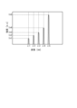
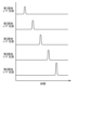
- FIG. 7 is a diagram showing the relationship between the wavelength and intensity of light in the embodiment.
- FIG. 8 is a diagram showing the results of a simulation of the intensity distribution of a pattern image formed in a resist when the mask is illuminated with illumination light in which the intensities of the lights L1 to L5 are adjusted.
- 9A and 9B are diagrams showing the results of simulating the NILS, uniformity, and number of wavelengths at each k2 when the numerical apertures NA are 0.4 and 0.5.
- FIGS. 10A and 10B are diagrams showing the results of simulating the NILS, uniformity, and number of wavelengths at each k2 for the numerical apertures NA of 0.6 and 0.7, respectively.
- FIG. 11(A) shows the results of simulating the NILS, uniformity, and number of wavelengths at each k2 when the numerical aperture NA is 0.8
- FIG. 11(B) shows the results of simulating the NILS and uniformity at each k2 when the numerical aperture NA is 1.35.
- FIG. 12 is a diagram for explaining lateral chromatic aberration.
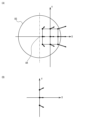
- FIG. 13A is a diagram showing the distribution of chromatic aberration of magnification in a projection optical system, and FIG.
- FIG. 13B is a diagram showing the distribution of chromatic aberration of magnification after scan averaging.
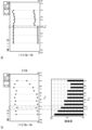
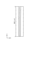
- 14(A) and 14(B) are diagrams showing the results of simulating the intensity distribution of a composite pattern image after scan averaging, where FIG. 14(A) shows the intensity distribution in a plane perpendicular to the Y-axis, and FIG. 14(B) shows the intensity distribution in a plane perpendicular to the X-axis.
- FIG. 15 is a diagram illustrating the emission timing of the lights L1 to L5.
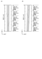
- FIG. 16 is a diagram showing the results of simulating the intensity of a composite pattern image in a cross section perpendicular to the X-axis, which is obtained by shifting the emission timings of the light beams L1 to L5 as shown in FIG. 17(A) to 17(C) are diagrams showing simulation results of the intensity of a composite pattern image formed in a resist by the methods of Comparative Examples 1 to 3, and FIG. 17(D) is a diagram showing simulation results of the intensity of a composite pattern image formed in a resist by the method of this embodiment.
- a pattern with a high aspect ratio that has a constant width in the depth direction and a small slope of the inner walls in a photosensitive material layer on a substrate (such as a glass plate or semiconductor wafer).
- the exposure apparatus 100 will be described below with reference to Figures 1 to 16.
- FIG. 1 is a diagram showing a schematic configuration of an exposure apparatus 100 according to this embodiment.
- the exposure apparatus 100 is an exposure apparatus that uses a spatial light modulator (SLM) that modulates illumination light (exposure light) according to control by an exposure control unit 160, which will be described later.
- SLM spatial light modulator
- the exposure apparatus 100 includes an illumination system 110, a pattern generating device 120, a projection optical system 130, a stage device 140, an alignment detection system 150, and an exposure control unit 160.
- the two mutually orthogonal directions in a horizontal plane are the X direction and the Y direction
- the direction orthogonal to the X direction and the Y direction is the Z direction.
- the rotation (tilt) directions around the X axis, Y axis, and Z axis are the ⁇ x direction, the ⁇ y direction, and the ⁇ z direction, respectively.
- the X direction is the scanning direction.
- the illumination system 110 includes a light source unit 111, an illumination optical system 112, and a reflecting mirror 113.
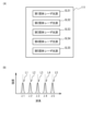
- FIG. 2(A) is a diagram showing a schematic configuration of the light source unit 111.
- the light source unit 111 includes a plurality of solid-state laser light sources.
- the light source unit 111 includes a first solid-state laser light source SLS1, a second solid-state laser light source SLS2, a third solid-state laser light source SLS3, a fourth solid-state laser light source SLS4, and a fifth solid-state laser light source SLS5.
- Each of the solid-state laser light sources SLS1 to SLS5 may be a solid-state laser device that amplifies laser light emitted from a laser light source such as a DFB semiconductor laser using a fiber optical amplifier and converts the wavelength of the amplified laser light using a wavelength conversion element.
- Such solid-state laser devices are disclosed, for example, in U.S. Patent Nos. 7,339,661, 7,974,320, 9,153,934, and 9,160,132.
- the first solid-state laser light source SLS1 emits illumination light (exposure light) L1 with a peak wavelength ⁇ 1 that illuminates the spatial light modulator 121 described below.
- the second solid-state laser light source SLS2 emits illumination light (exposure light) L2 with a peak wavelength ⁇ 2 that illuminates the spatial light modulator 121.
- the third solid-state laser light source SLS3 emits illumination light (exposure light) L3 with a peak wavelength ⁇ 3 that illuminates the spatial light modulator 121.
- the fourth solid-state laser light source SLS4 emits illumination light (exposure light) L4 with a peak wavelength ⁇ 4 that illuminates the spatial light modulator 121.
- the fifth solid-state laser light source SLS5 emits illumination light (exposure light) L5 with a peak wavelength ⁇ 5 that illuminates the spatial light modulator 121.
- illumination light L1 to illumination light L5 will be referred to as light L1 to light L5.
- FIG. 2(B) is a diagram showing the peak wavelengths ⁇ 1 to ⁇ 5 of light L1 to light L5 emitted from the first solid-state laser light source SLS1 to the fifth solid-state laser light source SLS5, respectively.
- the peak wavelengths ⁇ 1 to ⁇ 5 are discrete, and in this embodiment, ⁇ 1 ⁇ 2 ⁇ 3 ⁇ 4 ⁇ 5.
- the intensities of light L1 to L5 are shown as being the same, but the intensities of light L1 to L5 will be described later.
- the interval between adjacent peak wavelengths is constant, but this is not limited to this. The interval between adjacent peak wavelengths may be irregular.
- the first solid-state laser light source SLS1 to the fifth solid-state laser light source SLS5 change the intensity of the emitted light and the timing of light emission based on instructions from the exposure control unit 160.
- the instructions from the exposure control unit 160 may also be referred to as trigger signals.
- the illumination optical system 112 includes a shaping optical system for changing the illumination conditions, an optical integrator, a field stop, and a relay lens system (none of which are shown).
- the illumination optical system 112 emits illumination light (exposure light) IL that includes light L1 to L5 emitted from the light source unit 111. Since the illumination light IL includes light L1 to L5, it can be said to be light that has multiple peak wavelengths, or light that has a discrete wavelength distribution.
- the pattern generating device 120 generates a pattern to be formed on a wafer W placed on a stage 141 (described later) of the stage device 140 under the control of the exposure control unit 160.
- the wafer W includes a substrate 601 and a resist 602 (photosensitive material layer) applied onto the substrate 601.
- the pattern generating device 120 includes a spatial light modulator 121 and a driving unit 122.
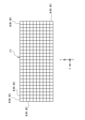
- FIG. 3 is a diagram showing an example of the spatial light modulator 121.
- the spatial light modulator 121 has a plurality of micromirror mechanisms M arranged in a matrix (two-dimensional, array) in the XY plane, for example.
- Each micromirror mechanism M has a micromirror M1 and a drive mechanism M2 provided on the side opposite the reflective surface of the micromirror M1.
- the drive mechanism M2 moves the micromirror M1 (up and down) along an axis extending in the Z direction.
- the drive unit 122 drives the drive mechanism M2 of each of the multiple micromirror mechanisms M in accordance with a control signal from the exposure control unit 160, and switches the micromirror M1 between an on state (on position) and an off state (off position).
- each micromirror M1 is too small to be resolved by the projection optical system 130, when all the micromirrors M1 are in the on state or all are in the off state in an area that can be resolved by the projection optical system 130, the zeroth-order diffracted light IL0 of the illumination light IL from the illumination system 110 that enters the area enters the projection optical system 130.
- 2 ⁇ 2 micromirrors M1 may be located in an area that can be resolved by the projection optical system 130.
- the illumination light (exposure light) IL from the illumination system 110 enters an area where micromirrors M1 in the on state and micromirrors M1 in the off state are alternately located, the illumination light IL is diffracted in this area, the zeroth-order diffracted light IL0 of the illumination light IL almost disappears, and the ⁇ 1st-order or higher diffracted light IL1 of the illumination light IL reaches a non-exposure optical path outside the projection optical system 130.
- the pattern generating device 120 gives a pattern to the illumination light IL by setting each of the multiple micromirrors M1 to either the on state or the off state.
- the surface on which multiple micromirrors M1 set to either the on state or the off state are arranged may be referred to as the light modulation surface of the spatial light modulator 121.
- the spatial light modulator 121 is not limited to the piston type described above, and may be, for example, a magneto-optic spatial light modulator (MOSLM: Magneto Optic Spatial Light Modulator) or a DMD (digital mirror device). Also, although the spatial light modulator 121 has been described as a reflective type that reflects the illumination light IL, the spatial light modulator 121 may be a transmissive type that transmits the illumination light IL, or a diffractive type that diffracts the illumination light IL. It is sufficient for the spatial light modulator 121 to be capable of spatially and temporally modulating the illumination light IL.
- MOSLM Magneto Optic Spatial Light Modulator
- the projection optical system 130 has a lens barrel 130s and multiple optical elements (not shown) arranged in a predetermined positional relationship inside the lens barrel 130s.
- the stage device 140 includes a stage (substrate stage) 141, a laser interferometer 142, and a stage driver 143.
- the stage 141 holds the wafer W via a wafer holder (not shown) located in the center of the upper surface.
- the stage 141 can be moved in the X, Y, and Z directions by a stage drive unit 143, and can also be rotated around an axis extending in the Z direction.
- the laser interferometer 142 constantly detects the position of the stage 141 in the X, Y, and ⁇ z directions with a resolution of, for example, about 0.5 to 1 nm by irradiating a measurement beam onto the reflecting surfaces provided on the end faces of the stage 141 in the X and Y directions.
- the stage driving unit 143 drives the stage 141 according to a control signal from the exposure control unit 160.
- the alignment detection system 150 is disposed on the side of the projection optical system 130.
- an imaging alignment sensor is used as the alignment detection system 150.
- the detailed configuration of the alignment detection system 150 is disclosed, for example, in the specification of U.S. Patent No. 5,637,129.
- the alignment detection system 150 detects street lines and position detection marks formed on the wafer W. The detection results of the street lines and position detection marks by the alignment detection system 150 are output to the exposure control unit 160.
- the exposure control unit 160 controls the operation of the illumination system 110, the pattern generating device 120, the stage device 140, etc. so as to form a predetermined exposure pattern on the wafer W, and projects an image of the light modulation surface of the spatial light modulator 121 via the projection optical system 130 onto the wafer W held on the stage 141.
- the illumination light IL reflected by the micromirror M1 of the spatial light modulator 121 i.e., the illumination light IL that has been given a pattern by the spatial light modulator 121, enters the projection optical system 130, and a reduced image (partial inverted image) of the pattern is formed in the projection area IA on the wafer W held on the stage 141.
- the exposure control unit 160 performs exposure using a step-and-scan method. During the scanning exposure, the exposure control unit 160 moves the stage 141 at an appropriate speed and scrolls the pattern generated by the spatial light modulator 121 in synchronization with the movement (i.e., changes the shape of the pattern generated by the spatial light modulator 121).
- the exposure apparatus 100 having the above configuration, the exposure apparatus disclosed in U.S. Patent No. 8,089,616, U.S. Patent Publication No. 2020/00257205, or WO 2005/081034 may be used.
- the exposure control unit 160 performs intensity control and emission timing control of the light L1 to L5.
- the intensity control will be described.
- the spatial light modulator 121 is illuminated with illumination light IL that includes multiple lights having different peak wavelengths, and the illumination light IL that has been given a pattern by the spatial light modulator 121 is projected onto the wafer W.
- the imaging positions are furthest from the projection optical system 130 in the order of light L5, light L4, light L3, light L2, and light L1 (in the order of light L5 to light L1).
- the imaging position of light L1 with wavelength ⁇ 1 is closest to the projection optical system 130, and the imaging position of light L5 with wavelength ⁇ 5 is furthest from the projection optical system 130.
- the imaging position of light L1 with wavelength ⁇ 1 is the position closest to the surface of resist 602 (photosensitive material layer) of wafer W (surface of wafer W), and the imaging position of light L5 with wavelength ⁇ 5 is the position farthest from the surface of resist 602.
- the positions at which the pattern images SI1 to SI5 (hereinafter also referred to as the pattern images of light L1 to L5) generated by the spatial light modulator 121 using light L1 to light L5 from the spatial light modulator 121 are formed are farthest from the surface of the resist 602 on the wafer W in the direction in which light L1 to light L5 travels, in the order of light L5, light L4, light L3, light L2, and light L1.
- the pattern images SI1 to SI5 of light L1 to light L5 overlap in the direction intersecting with the optical axis AX, as shown in FIG. 4A.
- the composite pattern image SIM obtained by combining the pattern images SI1 to SI5 of the five light beams L1 to L5 is an image with a large depth (length in the Z direction) relative to its width (length in the X direction).
- illumination light IL that includes multiple light beams L1 to L5 with different peak wavelengths, a pattern (groove) with a high aspect ratio can be formed in the resist 602 of the wafer W.
- the inventors have discovered that when the light beams L1 to L5 are emitted with the same intensity, the intensity of the pattern image of the light beam weakens the farther the image position of the light beam is from the surface of the resist 602 due to the attenuation coefficient of the resist 602. This point will be explained in more detail below.
- the inventors simulated the intensity of the pattern image formed in resist 502 applied to substrate 501 shown in FIG. 5(B) by light L1 to L5 passing through mask 503 when light L1 to L5 having the same intensity is used to illuminate mask 503 having the pattern shown in FIG. 5(A).
- mask 503 has a square pattern with each side measuring 200 nm.
- the shaded areas indicate that the light transmittance is 0.
- NA numerical aperture
- Figures 6(A) to 6(E) respectively show the results of simulating the intensity distribution of the pattern image of light L1 to light L5 in resist 502 when light L1 to light L5 have the same intensity.
- Figures 6(A) to 6(E) show the intensity distribution of the pattern image of light L1 to light L5 in resist 502 as contour lines, and the numbers on the contour lines indicate intensity. Note that the higher the number written on the contour lines, the higher the intensity.
- the intensities of the light L1 to light L5 when they enter the illumination optical system 112 are made different from one another. More specifically, as shown in FIG. 7, the intensity is increased as the imaging position is farther from the surface of the resist 602 in the traveling direction of the light L1 to light L5, that is, the position where the pattern image of the light L1 to light L5 is formed is farther from the surface of the resist 602. In other words, the intensity of the light irradiated onto the wafer W is increased for light where the pattern image is formed farther from the surface of the resist 602.
- the formation positions of the pattern images of light L1 to light L5 are farther from the surface of the resist in the order of light L5 to light L1. Therefore, if the intensity of light L1 is In1, the intensity of light L2 is In2, the intensity of light L3 is In3, the intensity of light L4 is In4, and the intensity of light L5 is In5, then In1 ⁇ In2 ⁇ In3 ⁇ In4 ⁇ In5. As a result, the intensities of light L1 to light L5 irradiated to the wafer W increase in the order of light L5 to light L1.
- the intensities In1 to In5 of the light L1 to L5 can be adjusted, for example, by the exposure control unit 160 controlling the first solid-state laser light source SLS1 to the fifth solid-state laser light source SLS5.
- the intensities In1 to In5 of the light L1 to L5 may be adjusted, for example, by setting the first solid-state laser light source SLS1 to the fifth solid-state laser light source SLS5.
- the intensities In1 to In5 of the light L1 to L5 may be adjusted using a neutral density filter in addition to controlling or setting the first solid-state laser light source SLS1 to the fifth solid-state laser light source SLS5. Also, the intensities of the light L1 to L5 emitted from the first solid-state laser light source SLS1 to the fifth solid-state laser light source SLS5 may be the same, and the intensities In1 to In5 when incident on the illumination optical system 112 (intensities when irradiated onto the wafer W) may be set to In1 ⁇ In2 ⁇ In3 ⁇ In4 ⁇ In5 by a neutral density filter.
- Isum ⁇ Ini ⁇ I( ⁇ i)
- In1 0.077
- In2 0.116
- In3 0.164
- In4 0.232
- In5 0.411
- the interval ⁇ between the wavelengths of the light L1 to L5 is determined so that the NILS (Normalized Image Log Slope) in the X and Y directions of the composite pattern image obtained by combining the pattern images of each of the multiple lights is high, the unevenness in the intensity of the composite pattern image in the Z direction is small (high uniformity), and the number of wavelengths used is small.
- NILS Normalized Image Log Slope
- Cz represents the axial chromatic aberration
- NA represents the numerical aperture
- ⁇ represents a representative (specific) wavelength (e.g., 248 nm) within the range including the wavelengths ⁇ 1 to ⁇ 5 of the light L1 to L5.
- Figures 9(A) to 11(B) are diagrams showing the results of simulations of the NILS, uniformity, and number of wavelengths at each k 2 for numerical apertures NA of 0.4, 0.5, 0.6, 0.7, 0.8, and 1.35.
- the NILS of the composite pattern image in the X and Y directions is high, the unevenness of the intensity of the composite pattern image in the Z direction is small (high uniformity), and the number of wavelengths used is small. Therefore, as shown in FIG. 9(A), when the numerical aperture NA is 0.4, k2 is considered to be optimal at 1.6. As shown in FIG. 9(B), when the numerical aperture NA is 0.6, k2 is considered to be optimal at 1.4. As shown in FIG. 10(A), when the numerical aperture NA is 0.6, k2 is considered to be optimal at 1.2. As shown in FIG. 10(B), when the numerical aperture NA is 0.7, k2 is considered to be optimal at 1.4. As shown in FIG. 11(A), when the numerical aperture NA is 0.8, k2 is considered to be optimal at 1.2.
- k2 can be set to about 2.
- the projection optical system 130 is an off-axis optical system that is one-sided telecentric (the spatial light modulator 121 side is non-telecentric) in order to separate the optical paths at the reflective spatial light modulator 121.
- the exposure area of this off-axis optical system has the center of the exposure area of each light positioned at a position offset from the optical axis AX (center of the lens) of the projection optical system 130 in the X direction (scanning direction).
- the pattern images formed by each of the lights L1 to L5 are formed at positions offset from the optical axis AX of the projection optical system 130. This causes an offset in the chromatic aberration of magnification in the X direction.
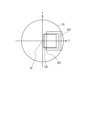
- FIG. 13(A) shows the distribution of the chromatic aberration of magnification of the projection optical system 130
- FIG. 13(B) shows the distribution of the chromatic aberration of magnification after scan averaging when scanning in the +X direction.
- the arrows are vectors representing the chromatic aberration of magnification.
- the vector representing the chromatic aberration of magnification can be expressed as (a ⁇ x+b, a ⁇ y).
- a is the coefficient
- b is the offset
- x is the position in the X direction
- y is the position in the Y direction.
- Figures 14(A) and 14(B) show the results of simulating the intensity distribution of the composite pattern image formed in the resist 502 after scan averaging.
- Figure 14(B) shows the intensity distribution in a plane perpendicular to the Y-axis.
- the timings at which the lights L1 to L5 are emitted are made different from one another. More specifically, the farther the position of the pattern image formed by each of the lights L1 to L5 is from the surface of the resist 602 in the traveling direction of the lights L1 to L5, the later the emission timing is made.
- the exposure control unit 160 controls the emission timing of the light L1 to the light L5 from the first solid-state laser light source SLS1 to the fifth solid-state laser light source SLS5 so that the emission timing of the light L5 is the latest and the emission timing of the light L1 is the earliest.
- the light whose pattern image formation position is farthest from the surface of the resist 602 is irradiated with the resist 602 is delayed.
- the timing at which the light L1 is irradiated with the resist 602 is the earliest, and the timing at which the light L5 is irradiated with the resist 602 is the latest.
- the pattern images of the light L1 to the light L5 can be formed at approximately the same position in the scanning direction (+X direction).
- the formation position of the pattern image of light L1 and the formation position of the pattern image of light L2 differ by ⁇ X in the scanning direction (+X direction)
- by irradiating light L2 onto resist 602 at the timing when wafer W moves ⁇ X by scanning after light L1 is irradiated onto resist 602 it is possible to make the formation position of the pattern image of light L1 and the formation position of the pattern image of light L2 approximately coincident on wafer W in the scanning direction (+X direction).
- the scanning direction of the wafer W is the ⁇ X direction, the further the position where the pattern image is formed is from the surface of the resist 602, the earlier the timing of irradiating the resist 602 with light.
- the timing of instructions (trigger signals) to the multiple solid-state laser light sources SLS1 to SLS5 that emit light of different wavelengths from each other may be changed according to the scanning direction.
- Figure 16 shows the results of simulating the intensity of the composite pattern image after scan averaging in a cross section perpendicular to the Y axis, obtained by shifting the emission timing of light L1 to light L5 as shown in Figure 15.
- the exposure apparatus 100 includes an illumination optical system 112 that illuminates the spatial light modulator 121 with illumination light IL including light L1 to light L5 having different wavelengths ⁇ 1 to ⁇ 5, and a projection optical system 130 that projects an image of a pattern generated by the spatial light modulator 121 with the illumination light IL from the spatial light modulator 121 onto the wafer W.
- the projection optical system 130 forms an image of the pattern generated by the spatial light modulator 121 with the illumination light L1 to illumination light L5 from the spatial light modulator 121, respectively, and forms the pattern images of the illumination light L1 to illumination light L5 at a position farther from the surface of the wafer W in the order of the illumination light L1 to illumination light L5 in the traveling direction of the illumination light L1 to illumination light L5. Also, the intensity of the illumination light L1 to illumination light L5 irradiated onto the wafer W increases in the order of the illumination light L5 to illumination light L1.
- the positions where the pattern images of the illumination lights L1 to L5 are formed are positions farther from the surface of the wafer W in the direction of travel of the illumination lights L1 to L5 in the order of illumination lights L1 to L5.
- the intensities of the illumination lights L1 to L5 irradiated onto the wafer W are higher in the order of illumination light L5 to illumination light L1
- the problem that the intensity decreases the farther the position where the pattern image is formed is from the surface of the wafer W due to the attenuation intensity of the resist 602 can be solved, and a composite pattern image with uniform intensity in the depth direction of the resist 602 can be formed.
- Figures 17(A) to 17(C) are diagrams showing simulation results of the intensity of composite pattern images formed in resist 502 by the methods according to Comparative Examples 1 to 3
- Figure 17(D) is a diagram showing simulation results of the intensity of composite pattern images formed in resist 502 by the method according to this embodiment.
- FIG. 17(A) is a diagram showing a simulation result of the intensity of a composite pattern image formed in the resist 502 when the mask 503 is illuminated with one light having a predetermined peak wavelength and the wafer W is continuously moved about 2.3 ⁇ m in the depth direction during exposure (Comparative Example 1).
- FIG. 17(B) is a diagram showing a simulation result of the intensity of a composite pattern image formed in the resist 502 when the mask 503 is illuminated with two lights having different peak wavelengths (Comparative Example 2). Note that the two lights illuminate the mask 503 with the same intensity.
- FIG. 17(A) is a diagram showing a simulation result of the intensity of a composite pattern image formed in the resist 502 when the mask 503 is illuminated with one light having a predetermined peak wavelength and the wafer W is continuously moved about 2.3 ⁇ m in the depth direction during exposure (Comparative Example 1).
- FIG. 17(B) is a diagram showing a simulation result of the intensity of a composite pattern image formed in the resist 502
- FIG. 17(C) is a diagram showing a simulation result of the intensity of a composite pattern image formed in the resist 502 when the mask 503 is illuminated with five lights having different peak wavelengths (Comparative Example 3). Note that the five lights illuminate the mask 503 with the same intensity.
- FIG. 17(D) is a diagram showing a simulation result of the intensity of a composite pattern image formed in the resist 502 when the mask 503 is illuminated with five lights having different peak wavelengths by performing the intensity control according to this embodiment.
- the intensity control according to this embodiment makes it possible to form a composite pattern image having a uniform intensity distribution in the depth direction.
- the uniformity of intensity in the depth direction (1 ⁇ ) was 38.8% in Comparative Example 1 ( Figure 17(A)), 50.5% in Comparative Example 2 ( Figure 17(B)), 23.7% in Comparative Example 3 ( Figure 17(C)), and 1.2% in this embodiment ( Figure 17(D)).
- the exposure apparatus 100 includes an exposure control unit 160 that controls the light source unit 111 that supplies the illumination light IL to the illumination optical system 112, and the exposure control unit 160 performs control to delay the timing at which the illumination lights L1 to L5 are irradiated onto the wafer W in the order of illumination light L5 to illumination light L1.
- the positions where the pattern images of the illumination lights L1 to L5 are formed are positions farther from the optical axis AX of the projection optical system 130 in the scanning direction (X direction) in the order of illumination light L5 to illumination light L1. Therefore, by delaying the timing at which the illumination lights L1 to L5 are irradiated onto the wafer W in the order of illumination light L5 to illumination light L1, the wafer W is scanned, and the pattern images of the illumination lights L1 to L5 can be formed at approximately the same position in the scanning direction, forming a pattern with a high aspect ratio that is approximately parallel to the depth direction of the resist 602.
- the illumination light IL including light L1 with wavelength ⁇ 1 and light L2 with wavelength ⁇ 2 different from wavelength ⁇ 1
- the projection optical system 130 forms an image of the pattern generated by the spatial light modulator 121 with the illumination light L1 from the spatial light modulator 121, and forms an image of the pattern generated by the spatial light modulator 121 with the illumination light L2 from the spatial light modulator 121 at a position farther from the surface of the wafer W than the image of the pattern by the illumination light L1 in the traveling direction of the illumination light L2.
- the intensity of the illumination light L2 irradiated to the wafer W may be made higher than the intensity of the illumination light L1 irradiated to the wafer W.
- the exposure control unit 160 may perform control to delay the timing at which the illumination light L2 is irradiated to the wafer W compared to the timing at which the illumination light L1 is irradiated to the wafer W.
- the number of light beams contained in the illumination light IL may be determined based on the characteristics (attenuation coefficient, thickness) of the resist 602 on the wafer W, the aspect ratio of the pattern to be formed in the resist 602, and the like.
- the projection optical system 130 is used in which chromatic aberration correction is performed such that the image formation position moves away from the projection optical system 130 as the wavelength becomes longer, but the chromatic aberration correction state of the projection optical system may be a chromatic aberration correction state in which the image formation position moves away from the projection optical system 130 as the wavelength becomes shorter, or a chromatic aberration correction state in which the image formation position moves away from or closer to the projection optical system 130 as the wavelength moves away from a specific wavelength (for example, wavelength ⁇ 3).
- the projection optical system 130 is used in which chromatic aberration correction is performed such that the magnification increases as the wavelength becomes longer, but the chromatic aberration correction state of the projection optical system may be a chromatic aberration correction state in which the magnification increases as the wavelength becomes shorter, or a chromatic aberration correction state in which the magnification increases or decreases as the wavelength moves away from a specific wavelength (for example, wavelength ⁇ 3).
- the exposure control unit 160 performs both intensity control and emission timing control, but it may perform only one of the controls.
- emission timing control of the light L1 to L5 was described using the example of the projection optical system 130 being one-sided telecentric, but emission timing control is applicable not only when the projection optical system 130 is one-sided telecentric, but also when an offset remains in the chromatic aberration of magnification after scan averaging.
- the exposure apparatus 100 is an exposure apparatus that uses an SLM, but the exposure apparatus 100 may be an exposure apparatus that uses a reticle (photomask). In this case, the exposure apparatus 100 exposes the pattern formed on the reticle onto the resist (photosensitive material layer) of the wafer W.
- a composite pattern image having a uniform intensity distribution in the depth direction is formed, but a uniform intensity distribution may not always be ideal. In such cases, the necessary combination of wavelengths and intensities may be selected to achieve an ideal intensity distribution.
- the wavelength intervals of the lights L1 to L5 are equal, but they do not have to be equal. Also, in the above embodiment, it is preferable that the emission timing of the lights L1 to L5 is equal when the wavelength intervals of the lights L1 to L5 are equal, but they do not have to be equal. Also, when the wavelength intervals of the lights L1 to L5 are not equal, the emission timing of the lights L1 to L5 does not have to be equal.
- Exposure apparatus 111
- Light source unit 112
- Illumination optical system 121
- Projection optical system AX Optical axis L1 to L5
- Light IL Illumination light W Wafer 602 Resist
Landscapes
- Physics & Mathematics (AREA)
- General Physics & Mathematics (AREA)
- Engineering & Computer Science (AREA)
- Optics & Photonics (AREA)
- Plasma & Fusion (AREA)
- Exposure And Positioning Against Photoresist Photosensitive Materials (AREA)
Abstract
Description
Isum=ΣIni・I(λi)
により算出した。ここで、Ini(i=1~5)は、重み係数であり、I(λi)は、光Li(i=1~5)の固定レーザ光源射出時の強度である。したがって、Ini・I(λi)は、光Liのマスク503照明時の強度(又は光Liのレジスト502照射時の強度)である。図8のシミュレーションでは、In1=0.077、In2=0.116、In3=0.164、In4=0.232、In5=0.411とした。
ΔFocus=k2・λ/NA2=Cz・Δλ
∴Δλ=k2・λ/Cz・NA2
となり、波長間の間隔Δλはk2に換算することができる。ここで、Czは軸上色収差を表し、NAは開口数を表し、λは、光L1~L5の波長λ1~λ5を含む範囲内における代表的な(特定の)波長(例えば、248nmなど)を表す。
なお、ウエハWの走査方向が-X方向である場合には、パターン像の形成位置がレジスト602の表面から遠い光ほど、レジスト602への照射タイミングを早くすればよい。例えば、上述した米国特許第8089616号に開示されるように、走査方向を逆向きに切替えながらラスタースキャンで走査露光を行う場合には、互いに異なる波長の光を射出する複数の固体レーザ光源SLS1~SLS5への指示(トリガ信号)のタイミングを走査方向に応じて変更してもよい。
なお、上記実施形態では、波長が長くなるに従って像形成位置が投影光学系130から離れるような色収差補正がなされた投影光学系130を用いているが、投影光学系の色収差補正状態は、波長が短くなるに従って像形成位置が投影光学系130から離れるような色収差補正状態であってもよいし、特定の波長(例えば波長λ3)から波長が離れるに従って像形成位置が投影光学系130から離れる、或いは近づくような色収差補正状態であってもよい。同様に、上記実施形態では、波長が長くなるに従って倍率が大きくなるような色収差補正がなされた投影光学系130を用いているが、投影光学系の色収差補正状態は、波長が短くなるに従って倍率が大きくなるような色収差補正状態であってもよいし、特定の波長(例えば波長λ3)から波長が離れるに従って倍率が大きくなる、或いは小さくなるような色収差補正状態であってもよい。
111 光源ユニット
112 照明光学系
121 空間光変調器
130 投影光学系
AX 光軸
L1~L5 光
IL 照明光
W ウエハ
602 レジスト
Claims (15)
- 第1波長の第1露光光と前記第1波長とは異なる第2波長の第2露光光とを含む露光光で第1物体を照明することと、
前記第1物体からの前記露光光で前記第1物体のパターンの像を第2物体上に露光することと、
を含み、
前記露光することは、前記第1物体からの前記第1露光光で前記第1物体のパターンの第1像を形成することと、前記第1物体からの前記第2露光光で前記第1物体のパターンの第2像を、前記第2露光光の進行方向において前記第1像よりも前記第2物体の表面から遠い位置に形成することとを含み、
前記第2物体に照射される前記第2露光光の強度は、前記第2物体に照射される前記第1露光光の強度よりも高い、
露光方法。 - 前記露光することは、前記第1物体からの前記露光光を前記第2物体に投影する投影光学系によって前記第1及び第2像を形成することを含む、
請求項1に記載の露光方法。 - 前記投影光学系の光軸と交差する方向において、前記第2像は前記第1像と重なっている、
請求項2に記載の露光方法。 - 前記露光光は、前記第1及び第2露光光を含む複数の波長の露光光を含み、
前記複数の波長の前記露光光における隣接する波長間の差Δλは、k2を係数、NAを開口数、λを前記複数の波長を含む範囲内の特定の波長としたときに、
Δλ=k2×λ/NA2
で表され、k2=1.3~1.6である、
請求項1から請求項3のいずれか一項に記載の露光方法。 - 前記複数の波長の前記露光光の波長の間隔は等間隔である、請求項4に記載の露光方法。
- 前記第2露光光が前記第2物体に照射されるタイミングは、前記第1露光光が前記第2物体に照射されるタイミングとは異なる、
請求項1から請求項5のいずれか一項に記載の露光方法。 - 第1波長の第1露光光と前記第1波長とは異なる第2波長の第2露光光とを含む露光光で第1物体を照明することと、
前記第1物体からの前記露光光で走査方向に沿って移動する第2物体を露光することと、
を含み、
前記露光することは、前記第1物体からの前記第1露光光で前記第1物体のパターンの第1像を形成することと、前記第1物体からの前記第2露光光で前記第1物体のパターンの第2像を、前記第2露光光の進行方向において前記第1像よりも前記第2物体の表面から遠い位置に形成することとを含み、
前記第2露光光が前記第2物体に照射されるタイミングは、前記第1露光光が前記第2物体に照射されるタイミングとは異なる、
露光方法。 - 前記露光することは、前記第1物体からの前記露光光を前記第2物体に投影する投影光学系によって前記第1及び第2像を形成することを含む、
請求項7に記載の露光方法。 - 前記投影光学系は、前記第1物体側が非テレセントリックな光学系である、
請求項8に記載の露光方法。 - 前記第1像及び前記第2像は、前記投影光学系の光軸から外れた位置に形成される、
請求項8または請求項9に記載の露光方法。 - 前記第1物体は、前記パターンが形成されたマスク、又は前記パターンを生成した空間光変調器である、
請求項1から請求項10のいずれか一項記載の露光方法。 - 第1波長の第1露光光と前記第1波長とは異なる第2波長の第2露光光とを含む第2露光光とを含む露光光で第1物体を照明する照明光学系と、
前記第1物体からの前記露光光で前記第1物体のパターンの像を第2物体上に投影する投影光学系と、
を含み、
前記投影光学系は、前記第1物体からの前記第1露光光で前記第1物体のパターンの第1像を形成し、且つ前記第1物体からの前記第2露光光で前記第1物体のパターンの第2像を、前記第2露光光の進行方向において前記第1像よりも前記第2物体の表面から遠い位置に形成し、
前記第2物体に照射される前記第2露光光の強度は、前記第2物体に照射される前記第1露光光の強度よりも高い、
露光装置。 - 前記照明光学系に前記露光光を供給する光源に、前記第2物体に照射される前記第2露光光の強度を、前記第2物体に照射される前記第1露光光の強度よりも高くする制御を行わせる制御装置をさらに備える、
請求項12に記載の露光装置。 - 第1物体のパターンを第2物体上に走査露光する露光装置であって、
第1波長の第1露光光と前記第1波長とは異なる第2波長の第2露光光とを含む露光光で第1物体を照明する照明光学系と、
前記第1物体からの前記露光光を走査方向に沿って移動する第2物体上に投影する投影光学系と、
前記照明光学系に前記露光光を供給する光源を制御する制御装置と、
を備え、
前記投影光学系は、前記第1物体からの前記第1露光光で前記第1物体のパターンの第1像を形成し、且つ前記第1物体からの前記第2露光光で前記第1物体のパターンの第2像を、前記第2露光光の進行方向において前記第1像よりも前記第2物体の表面から遠い位置に形成し、
前記制御装置は、前記第2露光光が前記第2物体に照射されるタイミングを、前記第1露光光が前記第2物体に照射されるタイミングとは異ならせる制御を行う、
露光装置。 - 請求項1から請求項11のいずれか一項に記載の露光方法を用いて前記第2物体の感光性材料層を露光することと、
露光された前記感光性材料層を現像することによって生じるパターンをマスクとして前記第2物体の前記感光性材料層よりも内側を加工することと、
を含むデバイス製造方法。
Priority Applications (6)
| Application Number | Priority Date | Filing Date | Title |
|---|---|---|---|
| PCT/JP2023/004244 WO2024166268A1 (ja) | 2023-02-08 | 2023-02-08 | 露光方法、露光装置、及びデバイス製造方法 |
| KR1020257026059A KR20250133390A (ko) | 2023-02-08 | 2023-02-08 | 노광 방법, 노광 장치 및 디바이스 제조 방법 |
| JP2024575965A JPWO2024166268A1 (ja) | 2023-02-08 | 2023-02-08 | |
| CN202380093365.0A CN120641831A (zh) | 2023-02-08 | 2023-02-08 | 曝光方法、曝光装置及器件制造方法 |
| TW113103916A TW202503426A (zh) | 2023-02-08 | 2024-02-01 | 曝光方法、曝光裝置、以及元件製造方法 |
| US19/272,755 US20250341783A1 (en) | 2023-02-08 | 2025-07-17 | Exposure method, exposure device, and device manufacturing method |
Applications Claiming Priority (1)
| Application Number | Priority Date | Filing Date | Title |
|---|---|---|---|
| PCT/JP2023/004244 WO2024166268A1 (ja) | 2023-02-08 | 2023-02-08 | 露光方法、露光装置、及びデバイス製造方法 |
Related Child Applications (1)
| Application Number | Title | Priority Date | Filing Date |
|---|---|---|---|
| US19/272,755 Continuation US20250341783A1 (en) | 2023-02-08 | 2025-07-17 | Exposure method, exposure device, and device manufacturing method |
Publications (1)
| Publication Number | Publication Date |
|---|---|
| WO2024166268A1 true WO2024166268A1 (ja) | 2024-08-15 |
Family
ID=92262180
Family Applications (1)
| Application Number | Title | Priority Date | Filing Date |
|---|---|---|---|
| PCT/JP2023/004244 Ceased WO2024166268A1 (ja) | 2023-02-08 | 2023-02-08 | 露光方法、露光装置、及びデバイス製造方法 |
Country Status (6)
| Country | Link |
|---|---|
| US (1) | US20250341783A1 (ja) |
| JP (1) | JPWO2024166268A1 (ja) |
| KR (1) | KR20250133390A (ja) |
| CN (1) | CN120641831A (ja) |
| TW (1) | TW202503426A (ja) |
| WO (1) | WO2024166268A1 (ja) |
Citations (4)
| Publication number | Priority date | Publication date | Assignee | Title |
|---|---|---|---|---|
| JP2010256428A (ja) * | 2009-04-21 | 2010-11-11 | Hitachi High-Technologies Corp | 露光装置、露光光照射方法、及び表示用パネル基板の製造方法 |
| US20110267593A1 (en) * | 2010-05-03 | 2011-11-03 | Taiwan Semiconductor Manufacturing Company, Ltd. | Method and apparatus for maintaining depth of focus |
| WO2016194378A1 (ja) * | 2015-06-02 | 2016-12-08 | 株式会社アドテックエンジニアリング | 光源装置、露光装置及び光源制御方法 |
| JP2019530024A (ja) * | 2016-09-20 | 2019-10-17 | カール・ツァイス・エスエムティー・ゲーエムベーハー | マイクロリソグラフィのための投影露光方法および投影露光装置 |
-
2023
- 2023-02-08 JP JP2024575965A patent/JPWO2024166268A1/ja active Pending
- 2023-02-08 WO PCT/JP2023/004244 patent/WO2024166268A1/ja not_active Ceased
- 2023-02-08 CN CN202380093365.0A patent/CN120641831A/zh active Pending
- 2023-02-08 KR KR1020257026059A patent/KR20250133390A/ko active Pending
-
2024
- 2024-02-01 TW TW113103916A patent/TW202503426A/zh unknown
-
2025
- 2025-07-17 US US19/272,755 patent/US20250341783A1/en active Pending
Patent Citations (4)
| Publication number | Priority date | Publication date | Assignee | Title |
|---|---|---|---|---|
| JP2010256428A (ja) * | 2009-04-21 | 2010-11-11 | Hitachi High-Technologies Corp | 露光装置、露光光照射方法、及び表示用パネル基板の製造方法 |
| US20110267593A1 (en) * | 2010-05-03 | 2011-11-03 | Taiwan Semiconductor Manufacturing Company, Ltd. | Method and apparatus for maintaining depth of focus |
| WO2016194378A1 (ja) * | 2015-06-02 | 2016-12-08 | 株式会社アドテックエンジニアリング | 光源装置、露光装置及び光源制御方法 |
| JP2019530024A (ja) * | 2016-09-20 | 2019-10-17 | カール・ツァイス・エスエムティー・ゲーエムベーハー | マイクロリソグラフィのための投影露光方法および投影露光装置 |
Also Published As
| Publication number | Publication date |
|---|---|
| TW202503426A (zh) | 2025-01-16 |
| US20250341783A1 (en) | 2025-11-06 |
| KR20250133390A (ko) | 2025-09-05 |
| JPWO2024166268A1 (ja) | 2024-08-15 |
| CN120641831A (zh) | 2025-09-12 |
Similar Documents
| Publication | Publication Date | Title |
|---|---|---|
| KR100841424B1 (ko) | 간섭 패턴들을 감소시키기 위해 회절 광학기에 대해 빔을이동시키는 방법 | |
| JP5250121B2 (ja) | 高速可変減衰器としての干渉計の使用 | |
| JP4659000B2 (ja) | 測定された光学素子特性に基づくパターンデータの変更 | |
| JP2010199605A (ja) | 照明光学システム | |
| JP2007258716A (ja) | 露光装置、放射供給及びデバイス製造方法 | |
| JP5063740B2 (ja) | インコヒーレントな放射を生成する反射ループシステム | |
| JPWO2009078434A1 (ja) | 露光装置、露光方法、及びデバイス製造方法 | |
| JP2008211210A (ja) | マスクレスリソグラフィの反射型空間光変調器を照明するための光学系および方法 | |
| JP5044264B2 (ja) | パターニング用デバイスへの照明効率を改善する光学系 | |
| JP4814200B2 (ja) | 高分解能露光ツールの像コントラストの強化 | |
| JP5091817B2 (ja) | 電磁放射パルス幅制御装置及び電磁放射パルス幅制御方法 | |
| JP2009158911A (ja) | マスクレスリソグラフィで用いる干渉に基づいたパターニングデバイスの照明 | |
| WO2024262020A1 (ja) | 空間光変調ユニットおよび露光装置 | |
| KR20100095620A (ko) | 조명 광학계, 노광 장치, 및 디바이스 제조 방법 | |
| JP2008078652A (ja) | リソグラフィシステム、デバイス製造方法、及びマスク最適化方法 | |
| JP2009124143A (ja) | 薄いフィルム状の連続的に空間的に調整された灰色減衰器及び灰色フィルタ | |
| KR102953844B1 (ko) | 노광 장치, 노광 방법 및 플랫 패널 디스플레이의 제조 방법, 그리고 노광 데이터 작성 방법 | |
| US20250341783A1 (en) | Exposure method, exposure device, and device manufacturing method | |
| JP2008047887A (ja) | 光学インテグレータ | |
| TW201439589A (zh) | 空間光調變器及其驅動方法、以及曝光方法及裝置 | |
| JP6613826B2 (ja) | 光源装置、露光装置、光発生方法、照明方法、露光方法、およびデバイス製造方法 | |
| JP5353408B2 (ja) | 照明光学系、露光装置、およびデバイス製造方法 | |
| JP5188152B2 (ja) | 放射ビームのパルス間の均一性を向上させる方法 | |
| JP6558529B2 (ja) | 空間光変調器及びその使用方法、変調方法、露光方法及び装置、並びにデバイス製造方法 | |
| JP2010141151A (ja) | 光束分割素子、照明光学系、露光装置、およびデバイス製造方法 |
Legal Events
| Date | Code | Title | Description |
|---|---|---|---|
| 121 | Ep: the epo has been informed by wipo that ep was designated in this application |
Ref document number: 23921099 Country of ref document: EP Kind code of ref document: A1 |
|
| ENP | Entry into the national phase |
Ref document number: 2024575965 Country of ref document: JP Kind code of ref document: A |
|
| WWE | Wipo information: entry into national phase |
Ref document number: 2024575965 Country of ref document: JP |
|
| ENP | Entry into the national phase |
Ref document number: 1020257026059 Country of ref document: KR Free format text: ST27 STATUS EVENT CODE: A-0-1-A10-A15-NAP-PA0105 (AS PROVIDED BY THE NATIONAL OFFICE) |
|
| WWE | Wipo information: entry into national phase |
Ref document number: 1020257026059 Country of ref document: KR |
|
| WWE | Wipo information: entry into national phase |
Ref document number: 202380093365.0 Country of ref document: CN |
|
| NENP | Non-entry into the national phase |
Ref country code: DE |
|
| WWP | Wipo information: published in national office |
Ref document number: 202380093365.0 Country of ref document: CN |
|
| 122 | Ep: pct application non-entry in european phase |
Ref document number: 23921099 Country of ref document: EP Kind code of ref document: A1 |