WO2024161743A1 - 積層セラミックコンデンサ - Google Patents
積層セラミックコンデンサ Download PDFInfo
- Publication number
- WO2024161743A1 WO2024161743A1 PCT/JP2023/040243 JP2023040243W WO2024161743A1 WO 2024161743 A1 WO2024161743 A1 WO 2024161743A1 JP 2023040243 W JP2023040243 W JP 2023040243W WO 2024161743 A1 WO2024161743 A1 WO 2024161743A1
- Authority
- WO
- WIPO (PCT)
- Prior art keywords
- layer
- electrode
- internal electrode
- outer layer
- laminate
- Prior art date
- Legal status (The legal status is an assumption and is not a legal conclusion. Google has not performed a legal analysis and makes no representation as to the accuracy of the status listed.)
- Ceased
Links
Images




Classifications
-
- H—ELECTRICITY
- H01—ELECTRIC ELEMENTS
- H01G—CAPACITORS; CAPACITORS, RECTIFIERS, DETECTORS, SWITCHING DEVICES, LIGHT-SENSITIVE OR TEMPERATURE-SENSITIVE DEVICES OF THE ELECTROLYTIC TYPE
- H01G4/00—Fixed capacitors; Processes of their manufacture
- H01G4/30—Stacked capacitors
-
- H—ELECTRICITY
- H01—ELECTRIC ELEMENTS
- H01G—CAPACITORS; CAPACITORS, RECTIFIERS, DETECTORS, SWITCHING DEVICES, LIGHT-SENSITIVE OR TEMPERATURE-SENSITIVE DEVICES OF THE ELECTROLYTIC TYPE
- H01G4/00—Fixed capacitors; Processes of their manufacture
- H01G4/002—Details
- H01G4/005—Electrodes
- H01G4/012—Form of non-self-supporting electrodes
-
- H—ELECTRICITY
- H01—ELECTRIC ELEMENTS
- H01G—CAPACITORS; CAPACITORS, RECTIFIERS, DETECTORS, SWITCHING DEVICES, LIGHT-SENSITIVE OR TEMPERATURE-SENSITIVE DEVICES OF THE ELECTROLYTIC TYPE
- H01G4/00—Fixed capacitors; Processes of their manufacture
- H01G4/002—Details
- H01G4/018—Dielectrics
- H01G4/06—Solid dielectrics
- H01G4/08—Inorganic dielectrics
- H01G4/12—Ceramic dielectrics
-
- H—ELECTRICITY
- H01—ELECTRIC ELEMENTS
- H01G—CAPACITORS; CAPACITORS, RECTIFIERS, DETECTORS, SWITCHING DEVICES, LIGHT-SENSITIVE OR TEMPERATURE-SENSITIVE DEVICES OF THE ELECTROLYTIC TYPE
- H01G4/00—Fixed capacitors; Processes of their manufacture
- H01G4/002—Details
- H01G4/228—Terminals
- H01G4/232—Terminals electrically connecting two or more layers of a stacked or rolled capacitor
Definitions
- the present invention relates to a multilayer ceramic capacitor.
- Patent document 1 describes a technology in which a conductive resin layer is placed on top of an intermediate layer in an external electrode, and the resin relieves stress, preventing the occurrence of cracks in a multilayer ceramic capacitor while ensuring moisture resistance reliability.
- Patent Document 1 still leaves room for improvement in terms of preventing cracks from occurring in multilayer ceramic capacitors and reducing their size.
- the purpose of the present invention is to prevent cracks from occurring in multilayer ceramic capacitors and to reduce their size.
- the multilayer ceramic capacitor of the present invention comprises a laminate having a first main surface and a second main surface that face each other in the lamination direction, a first side surface and a second side surface that face each other in a width direction perpendicular to the lamination direction, and a first end surface and a second end surface that face each other in a length direction perpendicular to the lamination direction and the width direction, and at least two external electrodes arranged on at least two or more surfaces of the laminate.
- the laminate comprises an inner layer portion and two outer layer portions that are arranged to sandwich the inner layer portion in the lamination direction.
- the inner layer portion comprises a plurality of first dielectric layers stacked in the lamination direction, and a first internal electrode that is arranged between two first dielectric layers of the plurality of first dielectric layers and is exposed to at least one of the first side surface, second side surface, first end surface, and second end surface.
- Each outer layer portion includes at least one second dielectric layer and a second internal electrode that is arranged in contact with the at least one second dielectric layer and is exposed to at least one of the first side surface, the second side surface, the first end surface, and the second end surface.
- the length of the second internal electrode in the length direction is shorter than the length of the first internal electrode in the length direction, or the width of the second internal electrode in the width direction is shorter than the width of the first internal electrode in the width direction.
- the present invention makes it possible to prevent cracks from occurring in multilayer ceramic capacitors and to reduce their size.
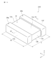
- FIG. 1 is a perspective view of a multilayer ceramic capacitor according to a first embodiment of the present invention
- 2 is a cross-sectional view taken along line II-II of FIG. 3 is a cross-sectional view taken along line III-III in FIG. 1 is an exploded perspective view of an inner layer portion according to a first embodiment of the present invention
- FIG. 3 is an enlarged view of region R in FIG.
- FIG. 2 is a cross-sectional view similar to FIG. 1 according to a modification of the first embodiment of the present invention
- FIG. 5 is a perspective view of a multilayer ceramic capacitor according to a second embodiment of the present invention
- 7A is a cross-sectional view taken along line VII-VII in FIG.
- FIG. 11 is a perspective view of a multilayer ceramic capacitor according to a third embodiment of the present invention
- 11 is a cross-sectional view taken along line XI-XI of
- FIG. 13 is an exploded perspective view of an inner layer portion according to a third embodiment of the present invention
- FIG. 13 is an exploded perspective view of an inner layer portion according to a modified example of the third embodiment of the present invention.
- 1 is a flowchart for explaining a method for manufacturing a multilayer ceramic capacitor according to a first embodiment of the present invention.
- each embodiment is an illustrative example of how the present invention can be implemented, and the present invention is not limited to the contents of the embodiment. It is also possible to combine the contents described in different embodiments, and the implementation in such cases is also included in the present invention.
- the drawings are intended to aid in understanding the specification, and may be drawn diagrammatically, and the dimensional ratios of the depicted components or between the components may not match the dimensional ratios of those components described in the specification. Components described in the specification may be omitted in the drawings, or the number of components may be omitted when drawn.
- Multilayer ceramic capacitor (first embodiment) A laminated ceramic capacitor according to a first embodiment of the present invention will now be described.
- FIG. 1 is a perspective view showing an example of a multilayer ceramic capacitor according to a first embodiment of the present invention.
- FIG. 2 is a cross-sectional view taken along line II-II in FIG. 1.
- FIG. 3 is a cross-sectional view taken along line III-III in FIG. 1.
- the multilayer ceramic capacitor 10 has a laminate 12, a first external electrode 30a, and a second external electrode 30b.
- the external electrode 30 when there is no need to distinguish between the first external electrode 30a and the second external electrode 30b, one of them may simply be referred to as the external electrode 30.
- the laminate 12 of this embodiment has a rectangular parallelepiped or approximately rectangular parallelepiped shape overall.
- the laminate 12 has a first main surface 12a and a second main surface 12b that face each other in the stacking direction X, a first side surface 12c and a second side surface 12d that face each other in the width direction Y, and a first end surface 12e and a second end surface 12f that face each other in the length direction Z.
- the stacking direction X, the width direction Y, and the length direction Z are mutually perpendicular.
- the corners and ridges of the laminate 12 are rounded.
- a corner is a portion where three adjacent faces of the laminate 12 intersect.
- a ridge is a portion where two adjacent faces of the laminate 12 intersect. Irregularities may be formed on some or all of the first main surface 12a and the second main surface 12b, the first side surface 12c and the second side surface 12d, and the first end surface 12e and the second end surface 12f.
- the laminate 12 includes an inner layer 13, a first outer layer 14a, and a second outer layer 14b.
- the first outer layer 14a and the second outer layer 14b may each simply be referred to as the outer layer 14.
- the inner layer portion 13 has a plurality of first inner electrodes 13a and a plurality of first dielectric layers 13b.
- the inner layer portion 13 is a portion located between the first inner electrode 13a closest to the first outer layer portion 14a and the first inner electrode 13a closest to the second outer layer portion 14b.
- the inner layer portion 13 is a portion located between the first inner electrode 13a adjacent to the first outer layer portion 14a and the first inner electrode 13a adjacent to the second outer layer portion 14b.
- the first dielectric layers 13b are stacked in the stacking direction X.
- the material of each of the first dielectric layers 13b is arbitrary.
- a dielectric ceramic mainly composed of BaTiO 3 can be used as the material of the first dielectric layers 13b.
- the material of the first dielectric layers 13b may have a plurality of crystal grains including a perovskite compound having BaTiO 3 as a basic structure.
- a dielectric ceramic mainly composed of other compounds such as CaTiO 3 , SrTiO 3 , CaZrO 3 , etc. may be used as the material of the first dielectric layers 13b.
- the material for the first dielectric layer 13b may be a material in which , as a subcomponent , for example, a Mn compound, an Fe compound, a Cr compound, a Co compound, or a Ni compound is added in a content range less than that of the main component to a main component such as BaTiO3, CaTiO3, SrTiO3, or CaZrO3.
- the thickness of the first dielectric layer 13b is arbitrary, but is preferably, for example, 10.0 ⁇ m or less.
- Each first internal electrode 13a is disposed between two adjacent dielectric layers in the stacking direction X among the plurality of dielectric layers included in the laminate 12.
- the first internal electrode 13a may be disposed between two adjacent first dielectric layers 13b in the stacking direction X among the plurality of first dielectric layers 13b.
- the first internal electrode 13a may be disposed between the first dielectric layer 13b disposed adjacent to each other in the stacking direction X and the second dielectric layer 29b of the outer layer portion 14.
- the first dielectric layer 13b is disposed between the two adjacent first internal electrodes 13a in the stacking direction X.
- the first internal electrode 13a is disposed in contact with the first dielectric layer 13b.
- the first internal electrode 13a in this embodiment is a plate-shaped electrode.
- the first internal electrode 13a extends in the longitudinal direction Z.
- the first internal electrode 13a has a first end exposed at either the first end face 12e or the second end face 12f, and a second end located inside the laminate 12.
- each first internal electrode 13a is exposed to either the first end face 12e or the second end face 12f of the laminate 12.
- the multiple first internal electrodes 13a include first internal electrodes 13a exposed to the first end face 12e and not exposed to the second end face 12f, and first internal electrodes 13a exposed to the end face of the second end face 12f and not exposed to the first end face 12e.
- the first internal electrodes 13a exposed to the first end face 12e and not exposed to the second end face 12f, and the first internal electrodes 13a exposed to the end face of the second end face 12f and not exposed to the first end face 12e are arranged alternately in the stacking direction X.
- FIG. 4 is an exploded perspective view of the inner layer portion 13.
- each first internal electrode 13a has an opposing electrode portion 15a and an extraction electrode portion 15b.
- the opposing electrode portion 15a is a portion of the first internal electrode 13a that faces another adjacent first internal electrode 13a in the stacking direction X.
- the extraction electrode portion 15b is a portion of the first internal electrode 13a other than the opposing electrode portion 15a.
- the opposing electrode portions 15a of two adjacent first internal electrodes 13a in the stacking direction X face each other via the first dielectric layer 13b, thereby forming a capacitance.
- each extraction electrode portion 15b is exposed to either the first end face 12e or the second end face 12f.
- the shape of the first internal electrode 13a is not particularly limited, but is preferably rectangular when viewed from the stacking direction X.
- the corners of the opposing electrode portion 15a may be chamfered or rounded.
- the corners of the extraction electrode portion 15b may be chamfered or rounded.
- the first internal electrode 13a preferably has a uniform thickness along the width direction Y, i.e., a dimension in the stacking direction X.
- the thickness of the end portion of the first internal electrode 13a in the width direction Y may be thicker than the thickness of the center portion of the first internal electrode 13a in the width direction Y.
- the main component of the first internal electrode 13a is Cu.
- the main component of the first internal electrode 13a is arbitrary, and may be other metals such as Ni, Pd, or Ag instead of Cu.
- the main component of the first internal electrode 13a may be an alloy of Ni, Pd, Ag, Cu, or the like with other metals.
- the thickness of the first internal electrode 13a is arbitrary, but is preferably, for example, 0.2 ⁇ m or more and 2.0 ⁇ m or less.
- the first outer layer portion 14a and the second outer layer portion 14b are disposed with the inner layer portion 13 sandwiched in the stacking direction X.
- the first outer layer portion 14a is disposed on one side of the stacking direction X with respect to the inner layer portion 13 (upper side in FIGS. 2 and 3). In other words, the first outer layer portion 14a is disposed on the first main surface 12a side with respect to the inner layer portion 13.
- the second outer layer portion 14b is disposed on the other side of the stacking direction X with respect to the inner layer portion 13 (lower side in FIGS. 2 and 3). In other words, the second outer layer portion 14b is disposed on the second main surface 12b side with respect to the inner layer portion 13.
- the outer layer portion 14 has a plurality of second internal electrodes 29a and a plurality of second dielectric layers 29b.
- the number of second internal electrodes 29a is not limited to multiple and may be one.
- the second dielectric layers 29b are stacked in the stacking direction X.
- the material of each second dielectric layer 29b is arbitrary.
- a dielectric ceramic mainly composed of BaTiO 3 can be used as the material of the second dielectric layer 29b.
- a dielectric ceramic mainly composed of other compounds such as CaTiO 3 , SrTiO 3 , CaZrO 3 , etc. may be used as the material of the second dielectric layer 29b.
- a compound such as a Mn compound, an Fe compound, a Cr compound, a Co compound, or a Ni compound may be added as an auxiliary component to the main component such as BaTiO 3 , CaTiO 3 , SrTiO 3, or CaZrO 3 in a content range less than that of the main component.
- the material of the second dielectric layer 29b may be made of a different main component from the material of the first dielectric layer 13b.
- the main component of the second dielectric layer 29b has a lower dielectric constant than the main component of the first dielectric layer 13b, the distance between the area that forms the most capacitance and the substrate can be increased, which has the effect of suppressing squeal.
- the dielectric constant of the second dielectric layer 29b is lower than that of the first dielectric layer 13b, the capacitance formed in the inner layer portion 13 can be made larger than the capacitance formed in the outer layer portion 14. In other words, the inner layer portion 13 can be made the area that forms the most capacitance in the multilayer ceramic capacitor 10.
- the distance between the substrate and the area that forms the most capacitance can be increased, compared to when the area that forms the most capacitance in the multilayer ceramic capacitor 10 is the outer layer portion 14. Therefore, the vibration generated in the inner layer portion 13 is less likely to be transmitted to the substrate, so that the generation of noise due to the vibration of the substrate can be suppressed.
- Each second internal electrode 29a is disposed between two of the multiple second dielectric layers 29b that are adjacent to each other in the stacking direction X.
- the second internal electrode 29a is disposed in contact with the second dielectric layer 29b.
- the second internal electrode 29a in this embodiment is a plate-shaped electrode.
- the second internal electrode 29a extends in the longitudinal direction Z.
- the second dielectric layer 29b has a first end exposed at either the first end face 12e or the second end face 12f, and a second end located inside the laminate 12.
- the length of the second internal electrode 29a i.e., the dimension in the longitudinal direction Z, is shorter than the length L1 of the first internal electrode 13a.
- the length L2 of the second internal electrode 29a of the first outer layer 14a is shorter than the length L1 of the first internal electrode 13a.
- the length L3 of the second internal electrode 29a of the second outer layer 14b is shorter than the length L1 of the first internal electrode 13a.
- the width of the second internal electrode 29a i.e., the dimension in the width direction Y, is narrower than the width W1 of the first internal electrode 13a.
- the width W2 of the second internal electrode 29a in the first outer layer portion 14a is narrower than the width W1 of the first internal electrode 13a.
- the width W3 of the second internal electrode 29a in the second outer layer portion 14b is narrower than the width W1 of the first internal electrode 13a.
- the second internal electrodes 29a are exposed to the first end face 12e or the second end face 12f of the laminate 12.
- the second internal electrodes 29a include second internal electrodes 29a exposed to the first end face 12e and not exposed to the second end face 12f, and second internal electrodes 29a exposed to the end face of the second end face 12f and not exposed to the first end face 12e.
- the second internal electrodes 29a exposed to the first end face 12e and not exposed to the second end face 12f and the second internal electrodes 29a exposed to the end face of the second end face 12f and not exposed to the first end face 12e are arranged alternately in the lamination direction X.
- the second internal electrodes 29a face each other in the outer layer portion 14 via the second dielectric layer 29b, thereby forming a capacitance.
- the two second internal electrodes 29a may be arranged without overlapping each other in the stacking direction X.
- the two second internal electrodes 29a may be arranged on the same plane.
- the two second internal electrodes 29a may have a second internal electrode 29a with one end exposed to the first end face 12e and the other end not exposed to the second end face 12f, and a second internal electrode 29a with one end exposed to the second end face 12f and the other end not exposed to the first end face 12e.
- FIG. 5 is an enlarged view of region R in FIG. 1.
- the second outer layer portion 14b has a similar configuration.
- the second dielectric layer 29b of the outer layer portion 14 includes a gap G.
- the porosity of the second dielectric layer 29b is lower in the region A1 closer to the inner layer portion 13 than in the region A2 farther from the inner layer portion 13.
- the porosity of the second dielectric layer 29b in the region A1 closer to the inner layer portion 13 is lower than the porosity of the second dielectric layer 29b in the region A2 farther from the inner layer portion 13.
- the porosity of the region A1 is preferably 1% or more and 4% or less
- the porosity of the region A2 is preferably higher than 4% and 10% or less.
- the porosity of the second dielectric layer 29b is lower in region A1 closer to the inner layer 13 than in region A2 farther from the inner layer 13, so that the voids act as a buffer and provide a stress relief effect, while the lower porosity in the region closer to the inner layer 13 prevents moisture penetrating through the voids from reaching the inner layer 13.
- the porosity of the second dielectric layer 29b included in the area closest to the inner layer 13 may be the lowest, and the porosity of the second dielectric layer 29b may increase as it approaches the area farther from the inner layer 13.
- a cut surface exposing each of the second dielectric layers 29b is observed at 6000x magnification using a scanning electron microscope (SEM).
- SEM scanning electron microscope
- An area with a field of view size of 19.5 ⁇ m x 10.5 ⁇ m is photographed in five locations so that the areas do not overlap, and the ratio of the area occupied by voids to the entire field of view is calculated as the porosity of each field of view by image analysis of each obtained SEM image, and the porosity is calculated from the average value over the five fields of view.
- the height T1 in the stacking direction X of the first outer layer 14a is lower than the height T2 in the stacking direction X of the second outer layer 14b.
- the mounting surface is the surface of the laminate 12 that faces the board when the multilayer ceramic capacitor 10 is mounted on the board.
- the coverage in the width direction Y x length direction Z of the first internal electrode 13a is 90% or more.
- the coverage in the width direction Y x length direction Z is defined as the ratio of the area inside the edge of the first internal electrode 13a minus the area of the gap provided in the first internal electrode 13a when the length x width surface formed by the length L and width W shown in Figure 1 of the laminate 12 is viewed in plan.
- the capacitance of the multilayer ceramic capacitor 10 increases when the surface coverage of the first internal electrode 13a in the width direction Y x length direction Z is high, but even if the surface coverage in the width direction Y x length direction Z is low, the two first dielectric layers 13b arranged on either side of the first internal electrode 13a in the stacking direction X are joined via a gap, so the bonding strength between the first dielectric layers 13b is high and delamination is less likely to occur.
- an insulating layer may be arranged on the first side surface 12c and the second side surface 12d of the laminate 12.
- the interface between the first internal electrode 13a and the first dielectric layer 13b, the interface between the first internal electrode 13a and the second dielectric layer 29b, and the interface between the second internal electrode 29a and the second dielectric layer 29b are covered with the insulating layer, and the intrusion of moisture into the laminate 12 can be suppressed.
- the insulating layer has the same or similar components as the first dielectric layer 13b or the second dielectric layer 29b.
- the adhesion between the insulating layer and the first dielectric layer 13b is improved.
- the adhesion between the insulating layer and the second dielectric layer 29b is improved.
- the insulating layer may also be arranged so as to be joined to the first internal electrode 13a and the second internal electrode 29a.
- the surface of the insulating layer that is not joined to the first internal electrode 13a and the second internal electrode 29a becomes the first side surface 12c and the second side surface 12d.
- the surface of the insulating layer that is arranged on the opposite side to the first internal electrode 13a and the second internal electrode 29a constitutes the first side surface 12c and the second side surface 12d of the laminate 12.
- the insulating layer preferably includes an inner layer that is the innermost in the width direction Y, and an outer layer that is the outermost in the width direction.
- the inner layer and the outer layer have an inner layer and an outer layer, and the boundary between them can be easily confirmed by observation with an optical microscope due to the difference in sintering properties between the inner layer and the outer layer. In other words, there is a boundary between the inner layer and the outer layer. There may be multiple boundaries.
- the insulating layer is not limited to a two-layer structure, but may be a three-layer or more structure.
- the layer located on the innermost side in the width direction Y is the inner layer
- the layer located on the outermost side in the width direction Y is the outer layer.
- the step layer 16 is disposed on the same plane as the first internal electrode 13a. If the step layer 16 is not disposed, a difference in thickness occurs between the portion where the first internal electrode 13a is disposed and the portion where the first internal electrode 13a is not disposed, and distortion may occur during pressing during the manufacturing process of the multilayer ceramic capacitor 10 described later. In contrast, in this embodiment, the step layer 16 can fill the step of the thickness of the first internal electrode 13a in the stacking direction X, so that distortion during pressing during the manufacturing process of the multilayer ceramic capacitor 10 can be alleviated. It is preferable that the step layer 16 has the same or approximately the same thickness as the first internal electrode 13a disposed on the same plane.
- the step layer 16 contains the same or approximately the same components as the first dielectric layer 13b.
- the step layer 16 may contain the same or approximately the same components as the first internal electrode 13a disposed on the same plane. In this case, the step layer 16 must be spaced apart from the first internal electrode 13a in the width direction Y and the length direction Z, and must be insulated from the first internal electrode 13a.
- the step layer 17 is disposed on the same plane as the second internal electrode 29a. If the step layer 17 is not disposed, a difference in thickness occurs in the outer layer portion 14 between the portion where the second internal electrode 29a is disposed and the portion where the second internal electrode 29a is not disposed, and distortion may occur during pressing during the manufacturing process of the multilayer ceramic capacitor 10 described below. In contrast, in this embodiment, the step layer 17 can fill the step of the thickness of the second internal electrode 29a in the lamination direction X, so that distortion during pressing during the manufacturing process of the multilayer ceramic capacitor can be alleviated. It is preferable that the step layer 17 has the same or approximately the same thickness as the second internal electrode 29a disposed on the same plane.
- the step layer 17 contains the same or approximately the same components as the second dielectric layer 29b.
- the step layer 17 may also contain the same or approximately the same components as the second internal electrode 29a disposed on the same plane. In this case, the step layer 17 must be spaced apart from the second internal electrode 29a in the width direction Y and the length direction Z, and must be insulated from the second internal electrode 29a.
- the second internal electrode 29a is preferably arranged at a position where the gap between the first internal electrode 13a and the first end face 12e or the second end face 12f is moved parallel to the stacking direction X.
- the second internal electrode 29a is preferably arranged at a position where it does not overlap with the first internal electrode 13a when viewed from the stacking direction X. This makes the height of the laminate 12 uniform in the stacking direction X, so that distortion caused by the step of the thickness of the first internal electrode 13a in the stacking direction X can be alleviated.
- External electrodes 30 are disposed on the first end face 12 e and the second end face 12 f of the laminate 12 .
- a first external electrode 30a is formed on the first end surface 12e side of the laminate 12.
- the first external electrode 30a is preferably arranged continuously on the first end surface 12e, the first main surface 12a, and the second main surface 12b of the laminate 12. It is more preferable that the first external electrode 30a is also arranged on the first side surface 12c and the second side surface 12d.
- the first external electrode 30a is joined to the first internal electrode 13a exposed on the first end surface 12e of the laminate 12 and the second internal electrode 29a exposed on the first end surface 12e of the laminate 12. As a result, the first external electrode 30a is electrically connected to the first internal electrode 13a and the second internal electrode 29a arranged on the first end surface 12e of the laminate 12.
- a second external electrode 30b is formed on the second end surface 12f side of the laminate 12.
- the second external electrode 30b is preferably arranged continuously on the second end surface 12f, the first main surface 12a, and the second main surface 12b of the laminate 12. It is even more preferable that the second external electrode 30b is also arranged on the first side surface 12c and the second side surface 12d.
- the second external electrode 30b is joined to the first internal electrode 13a exposed on the second end surface 12f of the laminate 12 and the second internal electrode 29a exposed on the second end surface 12f of the laminate 12. As a result, the second external electrode 30b is electrically connected to the first internal electrode 13a and the second internal electrode 29a arranged on the second end surface 12f of the laminate 12.
- the external electrode 30 has a base electrode layer 34 containing a conductive metal that is disposed on the laminate 12, a base plating layer 35 that is disposed so as to cover the surface of the base electrode layer 34, and a top plating layer 36 that is disposed so as to cover the surface of the base plating layer 35.
- the base plating layer 35 is a Ni plating layer
- the top plating layer 36 is a Sn plating layer.
- the base electrode layer 34 of the first external electrode 30a is formed on the first end surface 12e side of the laminate 12.
- the base electrode layer 34 of the first external electrode 30a is preferably arranged continuously on the first end surface 12e, the first main surface 12a, and the second main surface 12b of the laminate 12. It is more preferable that the base electrode layer 34 of the first external electrode 30a is also arranged on the first side surface 12c and the second side surface 12d.
- the base electrode layer 34 of the first external electrode 30a is joined to the first internal electrode 13a exposed on the first end surface 12e of the laminate 12 and the second internal electrode 29a exposed on the first end surface 12e of the laminate 12. As a result, the base electrode layer 34 of the first external electrode 30a is electrically connected to the first internal electrode 13a and the second internal electrode 29a arranged on the first end surface 12e of the laminate 12.
- the base electrode layer 34 of the second external electrode 30b is formed on the second end face 12f side of the laminate 12.
- the base electrode layer 34 of the second external electrode 30b is preferably arranged continuously on the second end face 12f, the first main face 12a, and the second main face 12b of the laminate 12. It is more preferable that the base electrode layer 34 of the second external electrode 30b is also arranged on the first side face 12c and the second side face 12d.
- the base electrode layer 34 of the second external electrode 30b is joined to the first internal electrode 13a exposed on the second end face 12f of the laminate 12 and the second internal electrode 29a exposed on the second end face 12f of the laminate 12. As a result, the base electrode layer 34 of the second external electrode 30b is electrically connected to the first internal electrode 13a and the second internal electrode 29a arranged on the second end face 12f of the laminate 12.
- the base electrode layer 34 includes at least one selected from a baked layer and a conductive resin layer, which are described below.
- the baking layer includes a glass component and a metal.
- the glass component includes at least one selected from B, Si, Ba, Mg, Al, Li, etc.
- the baking layer includes at least one metal selected from Cu, Ni, Ag, Pd, Ag-Ni alloy, and Au, for example.
- the baking layer may also include the same component as the first dielectric layer 13b instead of the glass component.
- the conductive resin layer may be disposed on the baked layer so as to cover the baked layer, or may be disposed directly on the laminate 12 .
- the conductive resin layer contains a thermosetting resin and a metal. Because the conductive resin layer contains a thermosetting resin, it is more flexible than a conductive layer made of, for example, a plating film or a fired conductive paste. Therefore, even if the multilayer ceramic capacitor 10 is subjected to a physical shock or a shock caused by a thermal cycle, the conductive resin layer functions as a buffer layer and can prevent cracks from occurring in the multilayer ceramic capacitor 10.
- the metal contained in the conductive resin layer can be Ag, Cu, or an alloy thereof. Also, a metal powder with an Ag-coated surface can be used as the metal contained in the conductive resin layer. It is preferable to use Cu or Ni as the metal powder with an Ag-coated surface. Also, Cu that has been treated to prevent oxidation can be used as the metal contained in the conductive resin layer.
- the reason for using Ag conductive metal powder as the conductive metal is that Ag has the lowest resistivity of all metals, making it suitable as an electrode material, and because Ag is a precious metal, it does not oxidize and has high weather resistance.
- the reason for using Ag-coated metal is that it is possible to make the base metal cheaper while still maintaining the above-mentioned properties of Ag.
- the metal contained in the conductive resin layer is mainly responsible for the electrical conductivity of the conductive resin layer. Specifically, when the conductive fillers contained in the conductive resin come into contact with each other, an electrical path is formed inside the conductive resin layer.
- the metal contained in the conductive resin layer can be spherical or flat, but it is preferable to use a mixture of spherical metal powder and flat metal powder.
- thermosetting resins such as epoxy resin, phenolic resin, urethane resin, silicone resin, polyimide resin, etc.
- epoxy resin which has excellent heat resistance, moisture resistance, and adhesion, is one of the most suitable resins for the conductive resin layer.
- the conductive resin layer preferably contains a hardener in addition to the thermosetting resin.
- a hardener in addition to the thermosetting resin.
- various known compounds such as phenol-based, amine-based, acid anhydride-based, and imidazole-based compounds can be used as the hardener for the epoxy resin.
- the multilayer ceramic capacitor 10 according to this embodiment can provide the following advantages.
- the porosity of the second dielectric layer 29b included in the region A1 close to the inner layer 13 is lower than the porosity of the second dielectric layer 29b included in the region A2 far from the inner layer 13.
- the laminated ceramic capacitor 10 can be made smaller than when a separate member for reinforcing the laminate 12 is provided in the laminated ceramic capacitor 10.
- the void ratio of the second dielectric layer 29b in the region A1 close to the inner layer portion 13 is relatively low, so that the moisture can be prevented from reaching the inner layer portion 13 through the voids G. As a result, the moisture resistance of the multilayer ceramic capacitor 10 can be improved.
- the height T2 in the stacking direction X of the second outer layer 14b closest to the second main surface 12b is higher than the height T1 in the stacking direction X of the first outer layer 14a closest to the first main surface 12a.
- the length L3 of the second internal electrode 29a in the second outer layer 14b closer to the second main surface 12b is shorter than the length L2 of the second internal electrode 29a in the second outer layer 14b closer to the first main surface 12a.
- the first internal electrode 13a is exposed on either the first end face 12e or the second end face 12f, but this is not limited to this.
- the first internal electrode 13a may be exposed on either the first side face 12c or the second side face 12d.
- the second internal electrode 29a is exposed on either the first end face 12e or the second end face 12f, but this is not limited to this.
- the second internal electrode 29a may be exposed on either the first side face 12c or the second side face 12d.
- the length L1 of the first internal electrode 13a is longer than the lengths L2, L3 of the second internal electrode 29a, and the width W1 of the first internal electrode 13a is wider than the widths W2, W3 of the second internal electrode 29a, but is not limited to this. If the length L1 of the first internal electrode 13a is longer than the lengths L2, L3 of the second internal electrode 29a, the width W1 of the first internal electrode 13a may be narrower than the widths W2, W3 of the second internal electrode 29a. If the width W1 of the first internal electrode 13a is wider than the widths W2, W3 of the second internal electrode 29a, the length L1 of the first internal electrode 13a may be shorter than the lengths L2, L3 of the second internal electrode 29a.
- the multilayer ceramic capacitor according to the second embodiment has a similar configuration to the multilayer ceramic capacitor according to the first embodiment, except for the shape and arrangement of the first internal electrodes, the shape and arrangement of the second internal electrodes, the number and configuration of the external electrodes, and the provision of surface electrodes on the surface of the laminate.
- configurations that are the same as or similar to those in the first embodiment are indicated by the same or similar reference symbols, and detailed descriptions thereof will be omitted.
- FIG. 7 is a perspective view of a multilayer ceramic capacitor 110 according to this embodiment.
- FIG. 8 is a cross-sectional view taken along line VII-VII in FIG. 7.
- FIG. 9 is an exploded perspective view of an inner layer portion 113 according to this embodiment.
- the multilayer ceramic capacitor 110 of this embodiment includes a laminate 112 and four external electrodes 130a, 130b, 130c, and 130d.
- the external electrode 130 when there is no need to distinguish between the four external electrodes 130a, 130b, 130c, and 130d, one of the four external electrodes 130a, 130b, 130c, and 130d may simply be referred to as the external electrode 130.
- the external electrodes 130 are disposed at each of the four corners of the laminate 112 when viewed along the stacking direction X.
- the external electrodes 130 are disposed so as to cover a portion of the first main surface 112a, a portion of the second main surface 112b, a portion of either the first side surface 112c or the second side surface 112d, and a portion of either the first end surface 112e or the second end surface 112f of the laminate 112.
- the external electrodes 130 may be disposed so as not to cover the first main surface 112a or the second main surface 112b in order to reduce the dimensions of the multilayer ceramic capacitor 110 in the stacking direction X.
- the external electrodes 130 are substantially L-shaped when viewed along the stacking direction X.
- the ratio W/L of the width W to the length L of the multilayer ceramic capacitor 110 of this embodiment is 0.85 or more and 1.0 or less.
- the height of the multilayer ceramic capacitor 110 that is, the dimension in the stacking direction X, is 120 ⁇ m or less.
- the ratio W/L may be less than 0.85 or greater than 1.0.
- the ratio W/L becomes closer to a substantially rectangular shape rather than a substantially square shape when viewed along the stacking direction X.
- the first internal electrode 113a of this embodiment has two extraction electrode portions 115b.
- Each extraction electrode portion 115b is exposed to either the first side surface 112c or the second side surface 112d, and either the first end surface 112e or the second end surface 112f.
- the extraction electrode portions 115b of the two first internal electrodes 113a facing each other in the stacking direction X are extracted to two different surfaces.
- the other first internal electrode 113a has an extraction electrode portion 115b drawn to the first side surface 112c and the first end surface 112e, and an extraction electrode portion 115b drawn to the second side surface 12d and the second end surface 12f
- the other first internal electrode 113a has an extraction electrode portion 115b drawn to the first side surface 12c and the second end surface 12f, and an extraction electrode portion 115b drawn to the second side surface 12d and the first end surface 12e.
- the extraction electrode portion 115b is continuously exposed from the end surface to the side surface, but is not limited to this and may be discontinuously exposed from the end surface to the side surface.
- the second internal electrode 129a is arranged at a position shifted from the lead electrode portion 115b of the first internal electrode 113a in the stacking direction X. In other words, the second internal electrode 129a is arranged at a position overlapping the lead electrode portion 115b of the first internal electrode 113a when viewed along the stacking direction X.
- the two second internal electrodes 129a may also be arranged on the same plane.
- the two second internal electrodes 129a arranged on the same plane are arranged without overlapping each other when viewed along the stacking direction X.
- the second internal electrode 129a By arranging the second internal electrode 129a on each of the first outer layer portion 114a and the second outer layer portion 114b, it is possible to ensure electrical connectivity between the first surface electrode 118 and the second surface electrode 119 described below and the first internal electrode 113a via the base electrode layer 134. Furthermore, by bonding the conductive components in the second internal electrode 129a and the external electrode 130, the bonding strength between the laminate 112 and the external electrode 130 can be improved.
- first surface electrodes 118 are arranged on the first main surface 112a of the laminate 112.
- second surface electrodes 119 are arranged on the second main surface 112b of the laminate 112.
- the first surface electrodes 118 are arranged at each of the four corners of the first main surface 112a.
- the second surface electrodes 119 are arranged at each of the four corners of the second main surface 112b.
- the first surface electrodes 118 and the second surface electrodes 119 are arranged at positions shifted in the stacking direction X from the lead electrode portion 115b of the first internal electrode 113a.
- first surface electrodes 118 and the second surface electrodes 119 are arranged at positions overlapping with the lead electrode portion 115b of the first internal electrode 113a when viewed along the stacking direction X.
- the first surface electrode 118 and the second surface electrode 119 are electrodes that do not form a capacitance.
- the first surface electrode 118 and the second surface electrode 119 may have the same shape and dimensions as the second internal electrode 129a. In this case, it is preferable that the first surface electrode 118 and the second surface electrode 119 are made of the same material as the second internal electrode 129a.
- the first surface electrode 118 and the second surface electrode 119 may be formed by a sputtering method.
- the first surface electrode 118 and the second surface electrode 119 preferably contain at least one selected from Ni, Cr, Cu, and Ti.
- the thickness of the first surface electrode 118 and the second surface electrode 119 formed by the sputtering method is preferably 50 nm or more and 400 nm or less. This allows the thickness of the first surface electrode 118 and the second surface electrode 119 in the stacking direction X to be sufficiently thin, and therefore the thickness of the multilayer ceramic capacitor 110 in the stacking direction X to be sufficiently thin.
- the thickness of the first surface electrode 118 and the second surface electrode 119 in the stacking direction X can be adjusted by changing the distance between the portion to be sputtered and the target.
- the thickness of the first surface electrode 118 and the second surface electrode 119 may be measured from an actual observation image, or may be measured by converting the thickness from a specified element using a calibration curve method for metal species using fluorescent X-rays.
- the first surface electrode 118 and the second surface electrode 119 may be sintered electrodes.
- a sintered electrode is an electrode containing the same type of dielectric component as the first dielectric layer 13b or the second dielectric layer 29b. That is, when the second dielectric layer 29b contains CaZrO3 , the first surface electrode 118 and the second surface electrode 119 contain, for example, Ca or Zr, CaZrO3. When the second dielectric layer 29b and the first dielectric layer 13b have different components, it is preferable that the first surface electrode 118 and the second surface electrode 119 contain the same type of component as the second dielectric layer 29b. This can make the adhesion between the second dielectric layer 29b and the first surface electrode 118 and the second surface electrode 119 stronger.
- the metal components in the fired electrodes preferably contain Ni.
- the first internal electrode 113a preferably contains Ni.
- the fired electrodes are formed by printing the conductive paste for Ni fired electrodes onto a dielectric sheet using screen printing or the like, followed by firing. At this time, by applying a thin layer of the conductive paste for Ni fired electrodes, or by reducing the dielectric components contained in the conductive paste for Ni fired electrodes, the Ni particles bond together during firing, forming a discontinuous fired electrode.
- a discontinuous fired electrode means that the fired electrodes are arranged discontinuously when viewed along the width direction Y.
- the external electrode 130 has a base electrode layer 134 containing a conductive metal arranged on the laminate 112, a base plating layer 135 arranged to cover the surface of the base electrode layer 134, and a top plating layer 136 arranged to cover the surface of the base plating layer 135.
- the base plating layer 135 is a Ni plating layer
- the top plating layer 136 is a Sn plating layer.
- the base electrode layer 134, base plating layer 135, and top plating layer 136 are arranged in this order, but they may also be arranged in the order of base electrode layer, top plating layer, base plating layer, and top plating layer.
- the base electrode layer 134 is preferably formed by a direct plating layer.
- a direct plating layer is a plating layer that directly covers the surface of the laminate 112. By using a direct plating layer as the base electrode layer 134, the thickness of the external electrode 130 in each direction can be reduced, allowing the laminate ceramic capacitor to be made smaller.
- the metal ratio per unit volume of the direct plating layer is preferably 99 volume percent or more.
- the direct plating may have two plating layers with different metal particle sizes. In this case, it is preferable that the plating layer with the larger metal particle size is arranged on the side closer to the laminate 12, and the plating layer with the smaller metal particle size is arranged on the side farther from the laminate 112.
- the multilayer ceramic capacitor 110 of the second embodiment provides the same effects as the multilayer ceramic capacitor 10 of the first embodiment.
- the multilayer ceramic capacitor 210 according to the third embodiment has a similar configuration to the multilayer ceramic capacitor 10 according to the first embodiment, except for its overall shape.
- configurations that are the same as or similar to those in the first embodiment are denoted by the same or similar reference characters, and detailed descriptions thereof will be omitted.
- FIG. 10 is a perspective view of a multilayer ceramic capacitor 210 according to this embodiment.
- FIG. 11 is a cross-sectional view taken along line XI-XI in FIG. 10.
- FIG. 12 is an exploded perspective view of an inner layer portion 13 according to this embodiment.
- the length L of the multilayer ceramic capacitor 210 is shorter than the width W of the multilayer ceramic capacitor 210.
- each first internal electrode 13a is exposed to either the first end face 12e or the second end face 12f. Also, as in a modified example of this embodiment shown in Figure 13, each first internal electrode 13a may be exposed to either the first end face 12e or the second end face 12f, the first side face 12c, and the second side face 12d.
- the multilayer ceramic capacitor 210 according to the third embodiment provides the same effects as the multilayer ceramic capacitor 10 according to the first embodiment.
- FIG. 6 is a flow chart for explaining the manufacturing method of a multilayer ceramic capacitor.
- a manufacturing method of the multilayer ceramic capacitor 10 according to the first embodiment will be described as an example.
- the multilayer ceramic capacitor 110 according to the second embodiment and the multilayer ceramic capacitor 210 according to the third embodiment can be manufactured by a manufacturing method similar to the manufacturing method of the multilayer ceramic capacitor 10 according to the first embodiment.
- the base electrode layer 34 is a baked layer.
- step S1 a dielectric sheet, a conductive paste for the internal electrodes, and a conductive paste for the external electrodes are prepared.
- the dielectric sheet, the conductive paste for the internal electrodes, and the conductive paste for the external electrodes contain a binder and a solvent.
- step S2 a conductive paste for the internal electrodes is printed on the dielectric sheet in a predetermined pattern to form a dielectric sheet for the inner layer portion on which the internal electrode pattern of the inner layer portion 13 is printed.
- the printing of the conductive paste for the internal electrodes on the dielectric sheet may be performed by, for example, screen printing or gravure printing.
- a conductive paste for the internal electrodes is printed in a predetermined pattern on the dielectric sheet to form a first outer layer dielectric sheet having the internal electrode pattern of the first outer layer 14a printed on the dielectric sheet.
- a conductive paste for the internal electrodes is printed in a predetermined pattern on the dielectric sheet to form a second outer layer dielectric sheet having the internal electrode pattern of the second outer layer 14b printed on the dielectric sheet.
- the printing of the conductive paste for the internal electrodes on the dielectric sheet may be performed by, for example, screen printing or gravure printing.
- step S3 multiple dielectric sheets for the inner layer are stacked and pressed in the stacking direction, for example by a hydrostatic press, to form a laminated block for the inner layer.
- step S3 a plurality of first outer layer dielectric sheets are stacked and pressed in the stacking direction, for example, by a hydrostatic press, to form a first outer layer laminate block. Specifically, the stacking and pressing of the first outer layer dielectric sheets are repeated to form the first outer layer laminate block. For this reason, the density of the first outer layer dielectric sheets at the beginning of stacking is high, and the density of the first outer layer dielectric sheets at the end of stacking is low. In other words, the first outer layer dielectric sheets stacked earlier have a lower porosity, and the dielectric sheets stacked later have a higher porosity.
- the dielectric sheets located on one side of the stacking direction have a lower porosity
- the dielectric sheets located on the other side of the stacking direction have a higher porosity.
- the amount of binder contained in the first outer layer dielectric sheets to be stacked may be adjusted.
- step S3 a plurality of second outer layer dielectric sheets are stacked and pressed in the stacking direction, for example, by a hydrostatic press, to form a second outer layer laminate block. Specifically, the stacking and pressing of the second outer layer dielectric sheets are repeated to form a second outer layer laminate block. For this reason, the density of the second outer layer dielectric sheets at the beginning of stacking is high, and the density of the second outer layer dielectric sheets at the end of stacking is low. In other words, the first second outer layer dielectric sheets stacked have a lower porosity, and the later second outer layer dielectric sheets stacked have a higher porosity.
- the dielectric sheets located on one side of the stacking direction have a lower porosity
- the dielectric sheets located on the other side of the stacking direction have a higher porosity.
- the amount of binder contained in the second outer layer dielectric sheets to be stacked may be adjusted.
- step S4 the first outer layer laminate block, the inner layer laminate block, and the second outer layer 14b laminate block are laminated and pressed in the lamination direction, for example by a hydrostatic press, to obtain a laminate block.
- the region of the first outer layer laminate block with a low porosity is positioned close to the inner layer laminate block, and the region of the high porosity is positioned far from the inner layer laminate block.
- the region of the second outer layer laminate block with a low porosity is positioned close to the inner layer laminate block, and the region of the high porosity is positioned far from the inner layer laminate block.
- step S5 the laminate block is cut to a predetermined size to cut out laminate chips.
- the corners and edges of the laminate chips may be rounded by barrel polishing or the like.
- step S6 the laminated chip is fired to form the laminate 12 according to this embodiment.
- step S7 a conductive paste containing a glass component and a metal is applied to the first end face 12e and the second end face 12f of the laminate 12, for example by dipping, and then a baking process is performed to form the base electrode layer 34.
- a plating layer is formed on the surface of the base electrode layer 34.
- the base plating layer 35 which is a Ni plating layer
- the top plating layer 36 which is a Sn plating layer
- the base plating layer 35 and the top plating layer 36 are formed, for example, by a barrel plating method.
- step S7 a conductive resin paste containing a thermosetting resin and a metal component is applied to the first end face 12e and the second end face 12f of the laminate 12, and then a heat treatment is performed to form a conductive resin layer.
- step S7 the first end face 112e and the second end face 112f of the laminate 112 are plated. It is preferable to use electrolytic plating as the plating process. It is preferable to use barrel plating as the plating method.
- first surface electrode 118 When the first surface electrode 118 is disposed on the first main surface 112a of the laminate 112 as in the second embodiment, a dielectric sheet having a pattern of the first surface electrode 118 printed thereon may be laminated on the outermost side in step S3 to form a first outer layer laminate block having the first surface electrode 118.
- second surface electrode 119 when the second surface electrode 119 is disposed on the second main surface 112b of the laminate 112, a dielectric sheet having a pattern of the first surface electrode 118 printed thereon may be laminated on the outermost side in step S3 to form a first outer layer laminate block having the first surface electrode 118.
- the first surface electrode 118 and the second surface electrode 119 have similar roughness, thickness, and denseness (coverage).
Landscapes
- Engineering & Computer Science (AREA)
- Power Engineering (AREA)
- Manufacturing & Machinery (AREA)
- Microelectronics & Electronic Packaging (AREA)
- Chemical & Material Sciences (AREA)
- Ceramic Engineering (AREA)
- Inorganic Chemistry (AREA)
- Fixed Capacitors And Capacitor Manufacturing Machines (AREA)
- Ceramic Capacitors (AREA)
Priority Applications (3)
| Application Number | Priority Date | Filing Date | Title |
|---|---|---|---|
| CN202380090013.XA CN120500732A (zh) | 2023-01-30 | 2023-11-08 | 层叠陶瓷电容器 |
| JP2024574274A JPWO2024161743A1 (https=) | 2023-01-30 | 2023-11-08 | |
| US19/081,304 US20250218691A1 (en) | 2023-01-30 | 2025-03-17 | Multilayer ceramic capacitor |
Applications Claiming Priority (2)
| Application Number | Priority Date | Filing Date | Title |
|---|---|---|---|
| JP2023-012053 | 2023-01-30 | ||
| JP2023012053 | 2023-01-30 |
Related Child Applications (1)
| Application Number | Title | Priority Date | Filing Date |
|---|---|---|---|
| US19/081,304 Continuation US20250218691A1 (en) | 2023-01-30 | 2025-03-17 | Multilayer ceramic capacitor |
Publications (1)
| Publication Number | Publication Date |
|---|---|
| WO2024161743A1 true WO2024161743A1 (ja) | 2024-08-08 |
Family
ID=92146111
Family Applications (1)
| Application Number | Title | Priority Date | Filing Date |
|---|---|---|---|
| PCT/JP2023/040243 Ceased WO2024161743A1 (ja) | 2023-01-30 | 2023-11-08 | 積層セラミックコンデンサ |
Country Status (4)
| Country | Link |
|---|---|
| US (1) | US20250218691A1 (https=) |
| JP (1) | JPWO2024161743A1 (https=) |
| CN (1) | CN120500732A (https=) |
| WO (1) | WO2024161743A1 (https=) |
Cited By (1)
| Publication number | Priority date | Publication date | Assignee | Title |
|---|---|---|---|---|
| US12573559B2 (en) | 2024-12-10 | 2026-03-10 | Kyocera Corporation | Electronic component |
Families Citing this family (1)
| Publication number | Priority date | Publication date | Assignee | Title |
|---|---|---|---|---|
| JP2025139797A (ja) * | 2024-03-13 | 2025-09-29 | 株式会社村田製作所 | 積層セラミックコンデンサ |
Citations (10)
| Publication number | Priority date | Publication date | Assignee | Title |
|---|---|---|---|---|
| JP2006203165A (ja) * | 2005-01-20 | 2006-08-03 | Samsung Electro Mech Co Ltd | 積層型チップキャパシタ |
| JP2006278557A (ja) * | 2005-03-28 | 2006-10-12 | Tdk Corp | 積層セラミック電子部品 |
| WO2007080852A1 (ja) * | 2006-01-13 | 2007-07-19 | Murata Manufacturing Co., Ltd. | 積層コンデンサ |
| JP2013251523A (ja) * | 2012-05-30 | 2013-12-12 | Samsung Electro-Mechanics Co Ltd | 積層チップ電子部品、その実装基板及び包装体 |
| JP2015061074A (ja) * | 2013-09-17 | 2015-03-30 | サムソン エレクトロ−メカニックス カンパニーリミテッド. | 積層セラミック電子部品及び積層セラミック電子部品の実装基板 |
| JP2016072279A (ja) * | 2014-09-26 | 2016-05-09 | 株式会社村田製作所 | 積層セラミックコンデンサ、これを含む積層セラミックコンデンサ連、および、積層セラミックコンデンサの実装体 |
| JP2020013974A (ja) * | 2018-07-20 | 2020-01-23 | サムソン エレクトロ−メカニックス カンパニーリミテッド. | 積層型キャパシタ |
| JP2021163834A (ja) * | 2020-03-31 | 2021-10-11 | 太陽誘電株式会社 | セラミック電子部品およびその製造方法 |
| JP2022523707A (ja) * | 2019-01-28 | 2022-04-26 | キョーセラ・エイブイエックス・コンポーネンツ・コーポレーション | 超広帯域性能を有する積層セラミックコンデンサ |
| JP2022142240A (ja) * | 2021-03-16 | 2022-09-30 | 株式会社村田製作所 | 積層セラミックコンデンサ |
-
2023
- 2023-11-08 JP JP2024574274A patent/JPWO2024161743A1/ja active Pending
- 2023-11-08 CN CN202380090013.XA patent/CN120500732A/zh active Pending
- 2023-11-08 WO PCT/JP2023/040243 patent/WO2024161743A1/ja not_active Ceased
-
2025
- 2025-03-17 US US19/081,304 patent/US20250218691A1/en active Pending
Patent Citations (10)
| Publication number | Priority date | Publication date | Assignee | Title |
|---|---|---|---|---|
| JP2006203165A (ja) * | 2005-01-20 | 2006-08-03 | Samsung Electro Mech Co Ltd | 積層型チップキャパシタ |
| JP2006278557A (ja) * | 2005-03-28 | 2006-10-12 | Tdk Corp | 積層セラミック電子部品 |
| WO2007080852A1 (ja) * | 2006-01-13 | 2007-07-19 | Murata Manufacturing Co., Ltd. | 積層コンデンサ |
| JP2013251523A (ja) * | 2012-05-30 | 2013-12-12 | Samsung Electro-Mechanics Co Ltd | 積層チップ電子部品、その実装基板及び包装体 |
| JP2015061074A (ja) * | 2013-09-17 | 2015-03-30 | サムソン エレクトロ−メカニックス カンパニーリミテッド. | 積層セラミック電子部品及び積層セラミック電子部品の実装基板 |
| JP2016072279A (ja) * | 2014-09-26 | 2016-05-09 | 株式会社村田製作所 | 積層セラミックコンデンサ、これを含む積層セラミックコンデンサ連、および、積層セラミックコンデンサの実装体 |
| JP2020013974A (ja) * | 2018-07-20 | 2020-01-23 | サムソン エレクトロ−メカニックス カンパニーリミテッド. | 積層型キャパシタ |
| JP2022523707A (ja) * | 2019-01-28 | 2022-04-26 | キョーセラ・エイブイエックス・コンポーネンツ・コーポレーション | 超広帯域性能を有する積層セラミックコンデンサ |
| JP2021163834A (ja) * | 2020-03-31 | 2021-10-11 | 太陽誘電株式会社 | セラミック電子部品およびその製造方法 |
| JP2022142240A (ja) * | 2021-03-16 | 2022-09-30 | 株式会社村田製作所 | 積層セラミックコンデンサ |
Cited By (1)
| Publication number | Priority date | Publication date | Assignee | Title |
|---|---|---|---|---|
| US12573559B2 (en) | 2024-12-10 | 2026-03-10 | Kyocera Corporation | Electronic component |
Also Published As
| Publication number | Publication date |
|---|---|
| CN120500732A (zh) | 2025-08-15 |
| JPWO2024161743A1 (https=) | 2024-08-08 |
| US20250218691A1 (en) | 2025-07-03 |
Similar Documents
| Publication | Publication Date | Title |
|---|---|---|
| KR101823246B1 (ko) | 적층 세라믹 전자 부품 및 그 실장 기판 | |
| JP7081543B2 (ja) | 積層セラミックコンデンサ | |
| JP2020053577A (ja) | 電子部品 | |
| JP2020077815A (ja) | 積層セラミックコンデンサ | |
| KR101973442B1 (ko) | 적층 세라믹 커패시터 및 그의 제조 방법 | |
| WO2024161743A1 (ja) | 積層セラミックコンデンサ | |
| US12518928B2 (en) | Multilayer ceramic electronic component | |
| US20250357048A1 (en) | Multilayer ceramic capacitor | |
| KR20240091618A (ko) | 적층형 전자 부품 | |
| US20240395467A1 (en) | Multilayer ceramic capacitor | |
| JP2023056513A (ja) | 積層型電子部品 | |
| WO2024236915A1 (ja) | 積層型電子部品および積層型電子部品の実装構造 | |
| JP7835297B2 (ja) | 積層セラミックコンデンサ | |
| US20260081076A1 (en) | Multilayer ceramic capacitor | |
| JP7736197B2 (ja) | 積層セラミックコンデンサ | |
| US20250372308A1 (en) | Multilayer ceramic capacitor | |
| WO2024018718A1 (ja) | 積層セラミック電子部品および積層セラミック電子部品の実装構造 | |
| WO2025018005A1 (ja) | 積層セラミック電子部品 | |
| WO2025018007A1 (ja) | 積層セラミック電子部品 | |
| WO2024018719A1 (ja) | 積層セラミック電子部品 | |
| WO2024224760A1 (ja) | 積層セラミック電子部品 | |
| WO2024209784A1 (ja) | 積層セラミックコンデンサ | |
| CN121241414A (zh) | 层叠陶瓷电容器 | |
| WO2025164085A1 (ja) | 積層セラミックコンデンサ | |
| CN121753127A (zh) | 层叠陶瓷电容器 |
Legal Events
| Date | Code | Title | Description |
|---|---|---|---|
| 121 | Ep: the epo has been informed by wipo that ep was designated in this application |
Ref document number: 23919878 Country of ref document: EP Kind code of ref document: A1 |
|
| WWE | Wipo information: entry into national phase |
Ref document number: 2024574274 Country of ref document: JP Ref document number: 202380090013.X Country of ref document: CN |
|
| WWP | Wipo information: published in national office |
Ref document number: 202380090013.X Country of ref document: CN |
|
| NENP | Non-entry into the national phase |
Ref country code: DE |
|
| 122 | Ep: pct application non-entry in european phase |
Ref document number: 23919878 Country of ref document: EP Kind code of ref document: A1 |