WO2024161546A1 - 電力変換装置および電力変換装置の制御方法 - Google Patents
電力変換装置および電力変換装置の制御方法 Download PDFInfo
- Publication number
- WO2024161546A1 WO2024161546A1 PCT/JP2023/003220 JP2023003220W WO2024161546A1 WO 2024161546 A1 WO2024161546 A1 WO 2024161546A1 JP 2023003220 W JP2023003220 W JP 2023003220W WO 2024161546 A1 WO2024161546 A1 WO 2024161546A1
- Authority
- WO
- WIPO (PCT)
- Prior art keywords
- phase
- command value
- power conversion
- carrier signal
- conversion device
- Prior art date
- Legal status (The legal status is an assumption and is not a legal conclusion. Google has not performed a legal analysis and makes no representation as to the accuracy of the status listed.)
- Ceased
Links
Images






Classifications
-
- H—ELECTRICITY
- H02—GENERATION; CONVERSION OR DISTRIBUTION OF ELECTRIC POWER
- H02M—APPARATUS FOR CONVERSION BETWEEN AC AND AC, BETWEEN AC AND DC, OR BETWEEN DC AND DC, AND FOR USE WITH MAINS OR SIMILAR POWER SUPPLY SYSTEMS; CONVERSION OF DC OR AC INPUT POWER INTO SURGE OUTPUT POWER; CONTROL OR REGULATION THEREOF
- H02M1/00—Details of apparatus for conversion
- H02M1/12—Arrangements for reducing harmonics from AC input or output
-
- H—ELECTRICITY
- H02—GENERATION; CONVERSION OR DISTRIBUTION OF ELECTRIC POWER
- H02M—APPARATUS FOR CONVERSION BETWEEN AC AND AC, BETWEEN AC AND DC, OR BETWEEN DC AND DC, AND FOR USE WITH MAINS OR SIMILAR POWER SUPPLY SYSTEMS; CONVERSION OF DC OR AC INPUT POWER INTO SURGE OUTPUT POWER; CONTROL OR REGULATION THEREOF
- H02M7/00—Conversion of AC power input into DC power output; Conversion of DC power input into AC power output
- H02M7/42—Conversion of DC power input into AC power output without possibility of reversal
- H02M7/44—Conversion of DC power input into AC power output without possibility of reversal by static converters
- H02M7/48—Conversion of DC power input into AC power output without possibility of reversal by static converters using discharge tubes with control electrode or semiconductor devices with control electrode
- H02M7/53—Conversion of DC power input into AC power output without possibility of reversal by static converters using discharge tubes with control electrode or semiconductor devices with control electrode using devices of a triode or transistor type requiring continuous application of a control signal
- H02M7/537—Conversion of DC power input into AC power output without possibility of reversal by static converters using discharge tubes with control electrode or semiconductor devices with control electrode using devices of a triode or transistor type requiring continuous application of a control signal using semiconductor devices only, e.g. single switched pulse inverters
- H02M7/539—Conversion of DC power input into AC power output without possibility of reversal by static converters using discharge tubes with control electrode or semiconductor devices with control electrode using devices of a triode or transistor type requiring continuous application of a control signal using semiconductor devices only, e.g. single switched pulse inverters with automatic control of output wave form or frequency
- H02M7/5395—Conversion of DC power input into AC power output without possibility of reversal by static converters using discharge tubes with control electrode or semiconductor devices with control electrode using devices of a triode or transistor type requiring continuous application of a control signal using semiconductor devices only, e.g. single switched pulse inverters with automatic control of output wave form or frequency by pulse-width modulation
-
- H—ELECTRICITY
- H02—GENERATION; CONVERSION OR DISTRIBUTION OF ELECTRIC POWER
- H02P—CONTROL OR REGULATION OF ELECTRIC MOTORS, ELECTRIC GENERATORS OR DYNAMO-ELECTRIC CONVERTERS; CONTROLLING TRANSFORMERS, REACTORS OR CHOKE COILS
- H02P27/00—Arrangements or methods for the control of AC motors characterised by the kind of supply voltage
- H02P27/04—Arrangements or methods for the control of AC motors characterised by the kind of supply voltage using variable-frequency supply voltage, e.g. inverter or converter supply voltage
- H02P27/06—Arrangements or methods for the control of AC motors characterised by the kind of supply voltage using variable-frequency supply voltage, e.g. inverter or converter supply voltage using DC to AC converters or inverters
- H02P27/08—Arrangements or methods for the control of AC motors characterised by the kind of supply voltage using variable-frequency supply voltage, e.g. inverter or converter supply voltage using DC to AC converters or inverters with pulse width modulation
-
- H—ELECTRICITY
- H02—GENERATION; CONVERSION OR DISTRIBUTION OF ELECTRIC POWER
- H02P—CONTROL OR REGULATION OF ELECTRIC MOTORS, ELECTRIC GENERATORS OR DYNAMO-ELECTRIC CONVERTERS; CONTROLLING TRANSFORMERS, REACTORS OR CHOKE COILS
- H02P29/00—Arrangements for regulating or controlling electric motors, appropriate for both AC and DC motors
- H02P29/50—Reduction of harmonics
Definitions
- This disclosure relates to a power conversion device that converts DC power to AC power and a method for controlling the power conversion device.
- Inverters are widely used as power conversion devices that convert DC power into AC power.
- the inverter compares a sinusoidal modulation signal with a triangular carrier signal to turn on and off semiconductor switching elements to output a sinusoidal phase voltage.
- harmonics are generated in the phase voltage due to switching.
- the frequency of the phase voltage is f s and the frequency of the carrier signal is f c
- harmonics are generated in the phase voltage, with a frequency component A having a frequency of f c ⁇ 2f s and a frequency component B having a frequency of f c ⁇ 4f s .
- the harmonics increase load losses and cause noise and torque pulsation.
- Patent Document 1 In the technology disclosed in Patent Document 1, harmonic components are superimposed on a sinusoidal modulation signal to disperse the ratio of frequency components A and B contained in the phase voltage. Patent Document 1 also explains that dispersing the ratio of frequency components A and B contained in the phase voltage can reduce load losses.
- the frequencies of frequency component A are 7f s and 11f s
- the frequencies of frequency component B are 5f s and 13f s .
- 7f s is a positive-phase component and is therefore 6f s
- 11f s is a negative-phase component and is therefore 12f s .
- 5f s is a negative-phase component and is therefore 6f s
- 13f s is a positive-phase component and is therefore 12f s .
- the present disclosure has been made in consideration of the above, and aims to provide a power conversion device that can effectively suppress noise and torque pulsation generated by inverter switching and reduce load losses due to harmonic components.
- the power conversion device disclosed herein is a power conversion device that supplies power to a multi-phase load based on a first command value, which is a sinusoidal phase voltage command value, and is characterized by comprising: a multi-phase inverter circuit in which legs, each of which has two semiconductor switching elements with reverse conduction function connected in series between the positive and negative terminals of a DC power source, are connected in parallel in the same number as the number of phases, and a terminal between the two semiconductor switching elements in each of the multiple legs is connected to each phase of the load; a modulation voltage generator that generates a second command value, which is a phase voltage command value for modulation composed of a fundamental wave component of the first command value and a harmonic component including at least one sine wave whose frequency is an odd multiple of the fundamental wave component; a carrier signal generator that generates a triangular wave carrier signal whose frequency is an odd multiple of the fundamental wave component of the first command value and whose median value is synchronized with
- the present disclosure has the effect of effectively suppressing noise and torque pulsation generated by inverter switching and reducing load losses due to harmonic components.
- FIG. 1 is a diagram showing a configuration of a power conversion device according to a first embodiment
- FIG. 2 is a diagram showing a configuration of a carrier signal generator shown in FIG. 1
- FIG. 3 is a diagram illustrating a carrier signal generated by the carrier signal calculator shown in FIG. 2
- FIG. 3 is a diagram showing an example of a carrier signal generated by the carrier signal calculator shown in FIG. 2
- FIG. 2 is an explanatory diagram of the operation of the gate signal generator shown in FIG.
- FIG. 13 is a diagram showing an example of a phase voltage output by a power conversion device when a sinusoidal second command value is provided to a gate signal generator
- FIG. 2 is a diagram showing a configuration of a modulation voltage generator shown in FIG. 1;
- FIG. 4 is a diagram showing waveforms of a second command value, a carrier signal, and an output phase voltage according to the first embodiment
- FIG. 13 is a diagram showing waveforms of a phase voltage command value, a carrier signal, and an output phase voltage in a comparative example of the first embodiment
- FIG. 1 is a diagram showing a WTHD of a power conversion device according to a first embodiment.
- FIG. 1 shows WTHD in a comparative example of the first embodiment.
- FIG. 1 is a diagram showing the magnitude of harmonic components included in an output phase voltage of a power conversion device according to a first embodiment.
- FIG. 13 is a diagram showing the magnitude of harmonic components included in an output phase voltage in a comparative example of the first embodiment;
- FIG. 1 is a diagram showing a configuration of a power conversion device according to a second embodiment
- FIG. 15 is a diagram showing a configuration of a modulation voltage generator shown in FIG. 14
- FIG. 13 is a diagram showing a configuration of a power conversion device according to a third embodiment.
- FIG. 17 is a diagram showing the configuration of a carrier signal generator shown in FIG. 16;
- FIG. 17 is a diagram showing a configuration of a modulation voltage generator shown in FIG. 16 .
- FIG. 13 is a diagram showing waveforms of a second command value, a carrier signal, and an output phase voltage according to the third embodiment.
- FIG. 13 is a diagram showing waveforms of a phase voltage command value, a carrier signal, and an output phase voltage in a comparative example of the third embodiment.
- FIG. 13 is a diagram showing WTHD of a power conversion device according to a third embodiment.
- FIG. 13 is a diagram showing WTHD in a comparative example of the third embodiment.
- FIG. 13 is a diagram showing the magnitude of harmonic components included in the output phase voltage of the power conversion device according to the third embodiment.
- FIG. 13 is a diagram showing the magnitude of harmonic components included in an output phase voltage in a comparative example of the third embodiment.
- FIG. 1 is a diagram showing a configuration example of a power conversion device when dedicated hardware is used.
- FIG. 1 is a diagram showing a configuration example of a power conversion device using a processor and a storage device;
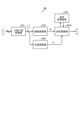
- Embodiment 1. 1 is a diagram showing a configuration of a power conversion device 1A according to embodiment 1.
- the power conversion device 1A has a multi-phase inverter circuit 3 connected to a DC power supply 2 and a motor 4 serving as a load, a modulation voltage generator 6A, a carrier signal generator 7A, and a gate signal generator 8.
- the multi-phase inverter circuit 3 converts the DC power of the DC power source 2 into multi-phase AC power and outputs it to the motor 4.
- the number of phases of the multi-phase inverter circuit 3 is three, and the phases are designated as u-phase, v-phase, and w-phase.
- the multi-phase inverter circuit 3 is configured such that legs 31, each of which has two semiconductor switching elements Q with reverse conduction functions connected in series, are connected in parallel for the number of phases. Since the number of phases of the multi-phase inverter circuit 3 is three, the multi-phase inverter circuit 3 has six semiconductor switching elements Q, and as shown in FIG.
- the six semiconductor switching elements Q are referred to as semiconductor switching elements Q up , Q un , Q vp , Q vn , Q wp , and Q wn , respectively.
- a series connection of a positive-side semiconductor switching element Q up and a negative-side semiconductor switching element Q un corresponding to the u-phase is called a leg 31u
- a series connection of a positive-side semiconductor switching element Q vp and a negative-side semiconductor switching element Q vn corresponding to the v-phase is called a leg 31v
- a series connection of a positive-side semiconductor switching element Q wp and a negative-side semiconductor switching element Q wn corresponding to the w-phase is called a leg 31w.
- each semiconductor switching element Q is composed of an IGBT (Insulated Gate Bipolar Transistor) and an anti-parallel diode.
- IGBT Insulated Gate Bipolar Transistor
- anti-parallel diode when a MOSFET (Metal-Oxide-Semiconductor Field-Effect Transistor), an RC (Reverse Conducting)-IGBT, or the like is used instead of the IGBT, the anti-parallel diode may be omitted.
- MOSFET Metal-Oxide-Semiconductor Field-Effect Transistor
- RC Reverse Conducting
- the motor controller 5 calculates first command values vu * , vv * , vw * which are sinusoidal phase voltage command values as voltages to be supplied to the motor 4, from the torque command value of the motor 4.
- the motor controller 5 outputs the calculated first command values vu * , vv * , vw * to the modulation voltage generator 6A and the carrier signal generator 7A, respectively.
- the modulation voltage generator 6A generates second command values m u , m v , and m w , which are phase voltage command values for modulation, based on the first command values v u * , v v * , and v w * .
- the modulation voltage generator 6A outputs the generated second command values m u , m v , and m w to the gate signal generator 8.
- the carrier signal generator 7A generates a triangular wave carrier signal c based on the first command values v u * , v v * , and v w * .
- the carrier signal generator 7A outputs the generated carrier signal c to the gate signal generator 8.
- the gate signal generator 8 generates gate signals g up , g un , g vp , g vn , g wp , and g wn that control the on and off of the semiconductor switching element Q of the multi-phase inverter circuit 3 by comparing the magnitude of the second command values m u , m v , and m w with the magnitude of the carrier signal c.
- the gate signals g up , g un , g vp , g vn , g wp , and g wn correspond to the semiconductor switching elements Q up , Q un , Q vp , Q vn , Q wp , and Q wn , respectively, and turn on or off the corresponding semiconductor switching element Q.
- gate signal g When there is no need to distinguish between the gate signals g up , g un , g vp , g vn , g wp , and g wn , they are simply referred to as gate signal g.
- FIG. 2 is a diagram showing the configuration of the carrier signal generator 7A shown in FIG. 1.
- the carrier signal generator 7A has a three-phase to two-phase converter 701, a phase calculator 702, and a carrier signal calculator 703A.
- the three-phase to two-phase converter 701 performs three-phase to two-phase conversion from first command values vu * , vv * , vw * on the three-phase coordinate to first command values v ⁇ * , v ⁇ * on the two-phase coordinate.
- the three-phase to two-phase converter 701 can perform three-phase to two-phase conversion using, for example, the following formula (1).
- the phase calculator 702 calculates the fundamental wave phase ⁇ v of the u-phase of the first command values v ⁇ * , v ⁇ * on the two-phase coordinate. Specifically, first, the phase of v ⁇ * is obtained by performing an arctangent calculation on the first command values v ⁇ * , v ⁇ * on the two-phase coordinate. This phase is the same as the phase of v u * . However, since the phase of v ⁇ * obtained by performing an arctangent calculation on the first command values v ⁇ * , v ⁇ * on the two-phase coordinate is based on a cosine signal, the phase based on a sin signal can be obtained by subtracting " ⁇ /2" from this phase.
- the fundamental wave components can be extracted by passing them through a low-pass filter, for example.
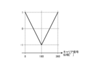
- the carrier signal calculator 703A first calculates a carrier signal c whose frequency is an odd number Kc times the fundamental wave component. Specifically, the phase of the carrier signal is generated by multiplying the fundamental wave phase ⁇ v by the odd number Kc. The carrier signal calculator 703A then generates a triangular wave carrier signal c as shown in FIG. 3.
- FIG. 3 is a diagram showing the carrier signal generated by the carrier signal calculator 703A shown in FIG. 2. Furthermore, the carrier signal calculator 703A performs phase synchronization control to correct the phase of the carrier signal c so that the median value of the triangular wave overlaps with the phase 0° of the phase voltage command value. In the example shown in FIG. 3, the median value of the triangular wave is zero.
- the carrier signal calculator 703A outputs the carrier signal c after phase synchronization control to the gate signal generator 8.
- the odd number Kc is set to 9, and the phase 270° of the carrier signal c is synchronized with the phase 0° of the phase voltage command value.
- the carrier signal becomes as shown in FIG. 4.
- FIG. 4 is a diagram showing an example of the carrier signal c generated by the carrier signal calculator 703A shown in FIG. 2.
- the carrier signal c is synchronized with the phase of the u-phase voltage, and a carrier signal c common to the three phases is used.
- the odd number Kc which determines the frequency of the carrier signal c, is set to a multiple of the number of phases, 3.
- the gate signal generator 8 compares the second command values mu , mv , and mw , which are phase voltage command values for modulation output by the modulation voltage generator 6A, with the carrier signal c to generate gate signals gup, gun, gvp, gvn , gwp, and gwn that control the on and off of the semiconductor switching elements Qup , Qun , Qvp , Qvn , Qwp , and Qwn of the multi- phase inverter circuit 3.
- Each of the gate signals gup , gun , gvp , gvn , gwp , and gwn has a high value "H" or a low value "L".
- the semiconductor switching element Q corresponding to that gate signal g is controlled to be on, and when the value of the gate signal g is "L”, the semiconductor switching element Q corresponding to that gate signal g is controlled to be off.
- FIG. 5 is an explanatory diagram of the operation of the gate signal generator 8 shown in FIG. 1.
- FIG. 5 shows u phases.
- the gate signal generator 8 compares the second command value m u with the carrier signal c to generate gate signals g up and g un . Specifically, when the second command value m u is greater than the carrier signal c, the value of the gate signal g up is set to "H” and the value of the gate signal g un is set to "L", and when the second command value m u is smaller than the carrier signal c, the value of the gate signal g up is set to "L” and the value of the gate signal g un is set to "H".
- the gate signals g up and g un are complementary to each other.
- FIG. 6 is a diagram showing an example of a phase voltage output by the power conversion device 1A when the sinusoidal second command value m u is given to the gate signal generator 8.
- FIG. 6 shows the waveforms of the phase voltages output for u phases when the gate signal g is generated from the second command values m u , m v , and m w, which are sinusoidal phase voltage command values for modulation, using the carrier signal c and the gate signal generator 8 to operate the multi-phase inverter circuit 3.
- the upper part of FIG. 6 shows the sinusoidal second command value m u and the triangular carrier signal c
- the lower part of FIG. 6 shows the output phase voltage v u output based on the sinusoidal second command value m u and the triangular carrier signal c.
- the waveform of the output phase voltage vu output by the power conversion device 1A is expressed as the sum of sine wave components and cosine wave components of various orders.
- the phase voltage is positively and negatively symmetrical from phase 0° to 180° and from phase 180° to 360°, even-order harmonic components are first removed.
- the phase voltage is subject to inversion from phase 0° to 90° and from phase 90° to 180°, and the cosine wave component is also removed. Therefore, when the carrier signal c of this embodiment is used, the harmonic components of the phase voltage are only odd-order sine wave components.
- FIG. 7 is a diagram showing the configuration of the modulated voltage generator 6A shown in FIG. 1.
- the modulated voltage generator 6A has a three-phase to two-phase converter 601, an amplitude calculator 602, a phase calculator 603, a waveform calculator 604A, and a waveform storage device 605.
- the three-phase to two-phase converter 601 performs three-phase to two-phase conversion of first command values vu * , vv * , vw * which are sinusoidal phase voltage command values on the three-phase coordinate system into first command values v ⁇ * , v ⁇ * on the two-phase coordinate system by the same process as the three-phase to two-phase converter 701.
- the three-phase to two-phase converter 601 outputs the first command values v ⁇ * , v ⁇ * on the two-phase coordinate system to the amplitude calculator 602 and the phase calculator 603, respectively.
- the amplitude calculator 602 first calculates the amplitude vphp of the first command values v ⁇ * , v ⁇ * from the first command values v ⁇ * , v ⁇ * on the two-phase coordinates. For example, the amplitude calculator 602 can calculate the amplitude vphp of the first command values v ⁇ * , v ⁇ * by using the following formula (2).
- the amplitude calculator 602 divides the amplitude vphp of the calculated first command values v ⁇ * , v ⁇ * by half the DC voltage, and converts it into amplitude M of the second command values mu , mv, mw , which are voltage command values for modulation, as shown in the following formula (3).
- the amplitude calculator 602 outputs the amplitude M, which is the calculation result, to the waveform calculator 604A.
- the phase calculator 603 calculates a fundamental wave phase ⁇ v of the u-phase of the first command values v ⁇ * , v ⁇ * on the two-phase coordinate system by the same process as the phase calculator 702.
- the phase calculator 603 outputs the fundamental wave phase ⁇ v , which is the calculation result, to the waveform calculator 604A.
- the waveform calculator 604A calculates the waveforms of the second command values m u , m v , and m w using the amplitude M and the fundamental wave phase ⁇ v of the u phase. Specifically, the waveforms of the second command values m u , m v , and m w corresponding to a quarter cycle of the fundamental wave from phase 0° to 90° of the first command values v u * , v v * , and v w * are stored in advance in the waveform storage device 605, and the second command values m u , m v , and m w are generated using the stored waveforms.
- the waveform calculator 604A reproduces the waveform of one cycle of the fundamental wave from the waveform corresponding to a quarter cycle of the fundamental wave by utilizing the fact that the phase voltage, that is, the second command values m u , m v , and m w , are positive-negative symmetrical from phase 0° to 180° and from phase 180° to 360°, and inversion symmetrical from phase 0° to 90° and from phase 90° to 180°.
- the waveform calculator 604A since the waveforms of the three-phase modulation phase voltage command values are waveforms that are shifted in phase from each other by 120°, the waveform calculator 604A generates a u-phase waveform using the fundamental wave phase ⁇ v of the u-phase, and then shifts the phase to generate second command values m u , m v , and m w for the three phases.
- the waveforms of the second command values m u , m v , m w stored in the waveform memory device 605 are generated so that the fundamental wave components of the phase voltages are as commanded and the harmonic components are optimized when the carrier signal c generated by the carrier signal generator 7A in this embodiment is used.
- the optimal second command values m u , m v , m w can be found by a simple method of superimposing only odd-order sine wave components, which are harmonic components, on the fundamental wave components of the first command values v u * , v v * , v w * .
- WO 2019/016901 discloses a method of superimposing a third harmonic on a three-phase inverter circuit.
- this method by superimposing harmonics whose frequency is an integer multiple of the number of phases, it is possible to supply a larger AC voltage to the load by effectively utilizing the DC side voltage without changing the output voltage on the load side of the multi-phase inverter circuit 3.
- harmonic components whose frequency is not an integer multiple of the number of phases i.e., sine waves, are also superimposed on the phase voltage command value. This makes it possible to optimize the frequency distribution of the harmonic components generated by the switching of the multi-phase inverter circuit 3.
- the second command values mu , mv , and mw are constant in a carrier half cycle, which is a period in which the carrier signal c changes from a minimum value to a maximum value or a period in which the carrier signal c changes from a maximum value to a minimum value.
- the quarter cycle of the fundamental wave stored in the waveform storage device 605 corresponds to 4.5 times the carrier half cycle, but in order to maintain the symmetry of the phase voltage waveform, the second command values mu , mv , and mw are set to zero in the first 0.5 cycle. Therefore, in this embodiment, it is necessary to optimize and store only four values corresponding to four intervals of the carrier half cycle, which makes optimization easy.
- the waveforms of the second command values m u , m v , and m w for one phase are stored for a quarter cycle of the fundamental wave.
- the period to be stored can be reduced.
- the phase of the v-phase voltage is ⁇ 120° to ⁇ 90°, i.e., 240° to 270°, during the period when the phase of the u-phase voltage is 0° to 30°.
- this waveform is obtained by inverting the waveform of the u-phase voltage during the period from 60° to 90° in the positive and negative directions.
- the phase of the w-phase voltage is ⁇ 240° to ⁇ 210°, i.e., 120° to 150°.
- this waveform is obtained by inverting the waveform of the u-phase voltage during the period from 30° to 60° in the time direction, i.e., in the phase direction. Therefore, when storing the waveforms of the second command values mu , mv , and mw for three phases, storing the waveforms for the phase period from 0° to 30° makes it possible to reproduce the waveforms for the period from 0° to 90°.
- the harmonic components of the phase voltages are optimized so as to minimize an objective function f obj expressed by the following equation (4).
- the harmonic components are optimized so that the root-sum-square value of the value obtained by dividing the n-th harmonic voltage vn by its order n, that is, the effective current value of the load, is minimized.
- n 6i ⁇ 1.
- specific frequency components here the 5th and 7th harmonic components, are assumed to excite the mechanical resonance of the load and cause large noise and torque pulsation, and are preferentially reduced by increasing the weighting of these order components.
- the weight kn in formula (4) is larger when n is 5 and when n is 7 than when n is other than 5 and 7, as expressed by the following formula (5). This makes it possible to reduce load loss while suppressing noise and torque pulsation.
- the number of phases of the multi-phase inverter circuit 3 and the motor 4 is three, and the three-phase waveforms are shifted in phase from each other by 120°, so no harmonic components that are multiples of three are generated. Furthermore, the voltage waveforms of each phase are symmetrical in positive and negative from phase 0° to 180° and from phase 180° to 360°, so no harmonic components that are multiples of two are generated. Furthermore, in optimization, harmonic components up to the 50th order are taken into account.
- FIG. 8 is a diagram showing the waveforms of the second command values m u , m v , m w , the carrier signal c, and the output phase voltage v u according to the first embodiment.
- the second command values m u , m v , and m w are composed of the fundamental wave components of the first command values v u * , v v * , and v w * and harmonic components including odd-order sine wave components.
- the harmonic components include sine wave components whose frequencies are not an integer multiple of the number of phases.
- the second command values m u , m v , and m w are superimposed with sine wave components whose frequencies are 3, 5, 7, 11, 13, 15, 17, 19, and 21 times that of the fundamental wave component.
- sine wave components with frequencies up to 21 times the fundamental wave component have been described here, sine wave components with even higher frequencies are superimposed on the second command values mu , mv , and mw .
- the u-phase output phase voltage vu is positive-negative symmetric between phases 0° to 180° and 180° to 360°, and is inversely symmetric between phases 0° to 90° and 90° to 180°.
- the second command values mu , mv , and mw are constant values in a half carrier cycle.
- Fig. 9 is a diagram showing waveforms of a phase voltage command value, a carrier signal c, and an output phase voltage vu in the comparative example of the first embodiment.
- the difference from the example of the first embodiment shown in Fig. 8 is that harmonic components are not superimposed on the phase voltage command value.
- the carrier signal c used is the same as that in the example shown in Fig. 8.
- the effective current value of the motor 4, which is the load is evaluated using WTHD, which is expressed by the following formula (6).
- the numerator of equation (6) is the square root of the sum of the squares of the nth harmonic voltage vn divided by its order n, that is, the value equivalent to the effective load current.
- FIG. 10 is a diagram showing the WTHD of the power conversion device 1A according to the first embodiment.
- FIG. 11 is a diagram showing the WTHD in a comparative example of the first embodiment. Comparing FIG. 10 and FIG. 11, it can be confirmed that the WTHD can be significantly reduced, particularly in the region where the amplitude M of the modulated voltage is large, and that the effective value of the load current, i.e., the loss, can be reduced.
- FIG. 12 is a diagram showing the magnitude of the harmonic components included in the output phase voltage of the power conversion device 1A according to the first embodiment.
- FIG. 13 is a diagram showing the magnitude of the harmonic components included in the output phase voltage in the comparative example of the first embodiment.
- the horizontal axis indicates the amplitude M
- the vertical axis indicates the frequency of the harmonics, which are expressed as the order relative to the fundamental wave.
- the magnitude of the harmonic components is shown by the value obtained by dividing the amplitude vph of the output phase voltage by half the DC voltage, and is shown by the shade of color.
- the power conversion device 1A can greatly reduce specific frequency components, here the fifth and seventh harmonic components, which are assumed to excite the mechanical resonance of the load and cause large noise and torque pulsation. It can be confirmed that the amplitudes of the fifth and seventh harmonic components are several percent or less of the amplitude M, which is the amplitude of the fundamental wave component, and are almost completely removed.
- the power conversion device 1A supplies power to the motor 4, which is a polyphase load, based on the first command values vu * , vv * , vw * , which are sinusoidal phase voltage command values.
- the power conversion device 1A includes a multi-phase inverter circuit 3 in which legs 31, each of which has two semiconductor switching elements Q having a reverse conducting function connected in series between positive and negative terminals of a DC power supply 2, are connected in parallel in the same number as the number of phases, and a terminal between the two semiconductor switching elements Q in each of the multiple legs 31 is connected to each phase of a motor 4 which is a load; a modulation voltage generator 6A that generates second command values m u , m v , m w which are phase voltage command values for modulation composed of a fundamental wave component of first command values v u * , v v * , v w * and a harmonic component including at least one sine wave whose frequency is an odd multiple of the fundamental wave component; and
- the triangular wave carrier signal c has the characteristic that its frequency is an odd multiple of the fundamental wave component of the first command values vu * , vv * , vw * and the median of the triangular wave is synchronized with phase zero of the fundamental wave component of the first command values vu * , vv * , vw *
- the generated phase voltage is positive-negative symmetrical from phase 0° to 180° and from phase 180° to 360°, and inversion symmetrical from phase 0° to 90° and from phase 90° to 180°, so that the phase voltage does not contain even-order harmonic components or cosine wave components, and the harmonic components contained in the phase voltage are only odd-order sine wave components.
- the second command values m u , m v , m w from the fundamental wave component of the first command values v u * , v v * , v w * and harmonic components including at least one sine wave whose frequency is an odd multiple of the fundamental wave component, it becomes possible to suppress the harmonic components contained in the output phase voltage.
- the frequency distribution of the harmonics generated by the switching of the multi-phase inverter circuit 3 can be optimized with a relatively simple configuration. This makes it possible to effectively suppress frequency components that generate load noise and torque pulsation, and at the same time reduce load losses due to the harmonic components.
- the harmonic components contained in the second command values mu , mv , and mw can include at least one sine wave whose frequency is an odd multiple of the fundamental wave component of the first command values vu * , vv * , and vw * and is not an integer multiple of the number of phases of the polyphase inverter circuit 3.
- the modulated voltage generator 6A stores second command values mu , mv, and mw corresponding to a quarter cycle of the fundamental wave components of the first command values vu * , vv * , and vw * in the waveform memory device 605, and is able to generate the second command values mu , mv , and mw using the waveform memory device 605.
- the generated phase voltages are positive-negative symmetrical between phases 0° to 180° and 180° to 360°, and inversion-symmetrical between phases 0° to 90° and 90° to 180°. Therefore, by utilizing the above features, it is possible to generate one period of the second command values mu , mv, mw by simply storing the second command values mu , mv , mw corresponding to a quarter cycle of the fundamental wave component.
- the multiple of the frequency of the fundamental component of the carrier signal c can be an odd number and an integer multiple of the number of phases of the multi-phase inverter circuit 3. This makes it possible to synchronize the carrier signal c with the phase of the phase voltage of one of the phases and use a common carrier signal c across multiple phases.
- the modulation voltage generator 6A keeps the second command values mu , mv, and mw constant during the carrier half cycle, which is the period during which the carrier signal c changes from the minimum value to the maximum value or the period during which the carrier signal c changes from the maximum value to the minimum value. This makes it possible to reduce the number of values stored in the waveform storage device 605, and to suppress the required storage capacity.
- the second command values m u , m v , and m w are optimized so that the effective current value of the load is lower than when the second command values m u , m v , and m w do not contain harmonic components.
- the second command values m u , m v , and m w are optimized so that the amplitudes of predetermined frequency components, for example, the fifth and seventh harmonic components, are lower than when the second command values m u , m v , and m w do not contain harmonic components.
- Embodiment 2. 14 is a diagram showing a configuration of a power conversion device 1B according to the second embodiment.
- the power conversion device 1B has a multi-phase inverter circuit 3, a modulated voltage generator 6B, a carrier signal generator 7A, and a gate signal generator 8.
- the power conversion device 1B has a modulated voltage generator 6B instead of the modulated voltage generator 6A of the power conversion device 1A according to the first embodiment.
- a description of the parts common to the power conversion device 1A according to the first embodiment will be omitted, and the parts different from the power conversion device 1A will be mainly described.
- phase synchronous control in which the carrier signal c is synchronized with the phase of the phase voltage command value of the load, when the phase or frequency of the voltage to be supplied to the load changes transiently, an identification time is required to synchronize the carrier signal c with the phase voltage command value.
- the second command values m u , m v , and m w are generated based on the phase of the carrier signal c, so that while the phase of the carrier signal c is not completely synchronized with the first command values v u * , v v * , and v w * , the second command values m u , m v , and m w, i.e., the phase voltages of the load, are not synchronized with the first command values.
- the modulation voltage generator 6B has a function capable of quickly generating the second command values m u , m v , and m w synchronized with the first command values v u * , v v * , and v w * even when the phase or frequency of the first command values v u * , v v * , and v w * changes transiently.
- FIG. 15 is a diagram showing the configuration of the modulation voltage generator 6B shown in FIG. 14.
- the modulation voltage generator 6B has a three-phase to two-phase converter 601, an amplitude calculator 602, a phase calculator 603, a waveform calculator 604B, and an order amplitude memory device 606B.
- the modulation voltage generator 6B has a waveform calculator 604B instead of the waveform calculator 604A of the modulation voltage generator 6A in the first embodiment, and has an order amplitude memory device 606B instead of the waveform memory device 605.
- the order amplitude storage device 606B stores information on the optimized second command values m u , m v , and m w in advance. Specifically, the order amplitude storage device 606B stores the amplitude m 1 of the fundamental wave component of the second command values m u , m v , and m w for the amplitude M, the amplitude of the sine wave to be included as a harmonic component, and the multiple of the frequency of the sine wave to be included as a harmonic component with respect to the fundamental wave component.
- the harmonic components have frequencies three times, five times, and seven times the fundamental wave component, and their amplitudes are m 3 , m 5 , and m 7 , respectively.
- m 1 , m 3 , m 5 , and m 7 are stored in association with the respective values of the amplitude M, and the amplitude of the fundamental wave component with respect to the amplitude M is m 1 (M), and the amplitude of the sine wave with respect to the amplitude M is m 3 (M), m 5 (M), and m 7 (M).
- the harmonic components when the phase of the sine wave is 180° can be reproduced by setting the amplitude to a negative value.
- the second command values m u , m v , and m w optimized in the same manner as in the first embodiment and shown in Fig. 8 are used.
- four voltage command values for four intervals of the carrier half cycle are stored in order to reproduce the waveform of a quarter cycle of the fundamental wave component. Since the degree of freedom is four, the original optimal waveform can be reproduced by using the fundamental wave component and harmonic components of three frequencies.
- the waveform calculator 604B calculates the waveforms of the second command values m u , m v , and m w for the amplitude M.
- the second command value m u (M) of the u phase for the amplitude M can be calculated using the following formula (7).
- the waveforms of the three-phase second command values m u , m v , and m w are waveforms in which the phases of the fundamental wave components are shifted from each other by 120°
- the second command values m u , m v , and m w for the three phases can be generated using the fundamental wave phase ⁇ v of the u-phase.
- the second command values m u , m v , and m w of the first embodiment are reproduced by function approximation, so that first, the same effects as those of the first embodiment can be obtained.
- the effective current value of the load that is, the loss
- the modulated voltage generator 6B stores the amplitude m 1 of the fundamental wave component of the first command values v u * , v v * , v w * , the amplitude of the sine wave included in the harmonic component, and the multiple of the frequency of the sine wave included in the harmonic component relative to the fundamental wave component in the order amplitude storage device 606B, which is a storage device, and generates the second command values m u , m v , m w using the order amplitude storage device 606B.
- the voltage according to the first command values v u * , v v * , v w * can be supplied to the load. Therefore, it is possible to control the voltage supplied to the load with high accuracy and high response.
- the carrier signal generator 7A generates the carrier signal c whose frequency is nine times that of the fundamental component, and the second command values m u , m v , and m w include sine waves of three frequencies as harmonic components.
- the second command values m u , m v , and m w can include sine waves of three, five, and seven times the frequency of the fundamental component as harmonic components.
- the power conversion device 1B according to the second embodiment can achieve the remarkable effect of controlling the voltage supplied to the load with high precision and high responsiveness in addition to the effect of the first embodiment.
- Embodiment 3. 16 is a diagram showing a configuration of a power conversion device 1C according to a third embodiment.
- the power conversion device 1C has a multi-phase inverter circuit 3, a modulated voltage generator 6C, a carrier signal generator 7B, and a gate signal generator 8.
- the power conversion device 1C has a modulated voltage generator 6C instead of the modulated voltage generator 6A of the power conversion device 1A according to the first embodiment, and has a carrier signal generator 7B instead of the carrier signal generator 7A.
- a description of the parts common to the power conversion device 1A according to the first embodiment will be omitted, and the parts different from the power conversion device 1A will be mainly described.
- FIG. 17 is a diagram showing the configuration of the carrier signal generator 7B shown in FIG. 16.
- the carrier signal generator 7B has a three-phase to two-phase converter 701, a phase calculator 702, and a carrier signal calculator 703B.
- the carrier signal generator 7B has the carrier signal calculator 703B instead of the carrier signal calculator 703A of the carrier signal generator 7A according to the first embodiment.
- the function of the carrier signal calculator 703B is basically the same as that of the carrier signal calculator 703A.
- the difference from the carrier signal calculator 703A is that the carrier signal calculator 703B sets the odd number Kc to 15 and generates a carrier signal c whose frequency is 15 times that of the fundamental wave component.
- the carrier signal generator 7B synchronizes the median value of the triangular wave, specifically, the phase 270° of the carrier signal c, with the phase 0° of the first command values vu * , vv * , vw * , as with the carrier signal generator 7A.
- the carrier signal c is synchronized with the phase of the u-phase voltage, and a common carrier signal c is used for the three phases. For this reason, the odd number Kc that determines the frequency of the carrier signal c is set to a multiple of the number of phases, 3.
- FIG. 18 is a diagram showing the configuration of the modulated voltage generator 6C shown in FIG. 16.
- the modulated voltage generator 6C has a three-phase to two-phase converter 601, an amplitude calculator 602, a phase calculator 603, a waveform calculator 604C, and an order amplitude memory device 606C.
- the modulation voltage generator 6C has a waveform calculator 604C instead of the waveform calculator 604A of the modulation voltage generator 6A according to the first embodiment, and has an order amplitude memory device 606C instead of the waveform memory device 605.
- the order amplitude storage device 606C stores information on the optimized second command values m u , m v , and m w in advance. Specifically, the order amplitude storage device 606C stores the amplitude m 1 of the fundamental wave component of the second command values m u , m v , and m w for the amplitude M, the amplitude of the sine wave to be included as the harmonic component, and the multiple of the frequency of the sine wave to be included as the harmonic component with respect to the fundamental wave component.
- the harmonic components have six frequencies, 3 times, 5 times, 7 times, 9 times, 11 times, and 13 times the fundamental wave component, and the amplitudes are m 3 , m 5 , m 7 , m 9 , m 11 , and m 13 , respectively.
- m1 , m3 , m5 , m7 , m9 , m11 , and m13 are stored in association with each value of amplitude M, with m1 (M) being the amplitude of the fundamental wave component for amplitude M, and m3 (M), m5 (M), m7 (M), m9 (M), m11 (M), and m13 (M) being the amplitudes of the sine wave for amplitude M.
- the harmonic components when the phase of the sine wave is 180° can be reproduced by setting the amplitude to a negative value.
- the second command values m u , m v , and m w are constant in the carrier half cycle, which is the period in which the carrier signal c changes from the minimum value to the maximum value or the period in which the carrier signal c changes from the maximum value to the minimum value. It is also assumed that the waveforms of the second command values m u , m v , and m w are positive-negative symmetrical between phases 0° to 180° and 180° to 360°, and inversely symmetrical between phases 0° to 90° and 90° to 180°.
- the fundamental wave quarter cycle of the second command values m u , m v , and m w corresponds to 7.5 times the carrier half cycle, but in order to maintain the symmetry of the phase voltage waveform, the second command values m u , m v , and m w are set to zero in the first 0.5 cycle. Therefore, in this embodiment, it is sufficient to optimize only seven values corresponding to seven sections of the carrier half cycle, making optimization easy. Since the degree of freedom of the waveforms of the second command values m u , m v , and m w is seven, the original optimal waveform can be reproduced by using the fundamental wave component and six harmonic components.
- the harmonic components included in the second command value are optimized so as to minimize the objective function f obj shown in the following equation (8).
- the harmonic components are optimized so that the root-sum-square value of the value obtained by dividing the n-th harmonic voltage vn by its order n, that is, the effective current value of the load, is minimized.
- n 6i ⁇ 1.
- specific frequency components here the 11th and 13th harmonic components, are assumed to excite the mechanical resonance of the load and cause large noise and torque pulsation, and are preferentially reduced by increasing the weighting of these order components.
- the weight kn in formula (8) is larger when n is 11 and when n is 13 than when n is other than 11 and 13, as expressed by the following formula (9). This makes it possible to reduce load loss while suppressing noise and torque pulsation.
- the number of phases of the multi-phase inverter circuit 3 and the motor 4 is three, and the three-phase waveforms are shifted in phase from each other by 120°, so no harmonic components that are multiples of three are generated. Furthermore, the voltage waveforms of each phase are symmetrical in positive and negative from phase 0° to 180° and from phase 180° to 360°, so no harmonic components that are multiples of two are generated. Furthermore, in optimization, harmonic components up to the 50th order are taken into account.
- the waveform calculator 604C calculates the waveforms of the second command values m u , m v , and m w based on the amplitude M and the fundamental wave phase ⁇ v .
- the second command value m u (M) of the u-phase is calculated using the following formula (10).
- the waveform calculator 604C can generate the three-phase second command values m u , m v , and m w by using the fundamental wave phase ⁇ v of the u-phase.
- Fig. 19 is a diagram showing waveforms of the second command values m u , m v , m w , carrier signal c, and output phase voltage v u according to the third embodiment.
- the second command values m u , m v , m w are composed of the fundamental wave components of the first command values v u * , v v * , v w * , and harmonic components including odd-order sine wave components.
- the harmonic components include sine wave components whose frequencies are not integer multiples of the number of phases.
- Fig. 20 is a diagram showing waveforms of a phase voltage command value, a carrier signal c, and an output phase voltage vu in the comparative example of the third embodiment.
- the difference from the third embodiment shown in Fig. 19 is that a harmonic component is not superimposed on the phase voltage command value.
- the carrier signal c used is the same as the example shown in Fig. 19.
- FIG. 21 is a diagram showing the WTHD of the power conversion device 1C according to the third embodiment.
- FIG. 22 is a diagram showing the WTHD in a comparative example of the third embodiment. Comparing FIG. 21 with FIG. 22, it can be confirmed that the WTHD can be significantly reduced and the effective current value of the load, that is, the loss, can be reduced, particularly in the region where the amplitude M of the modulated voltage is large.
- the power conversion device 1C according to the third embodiment cannot reduce the WTHD compared to the comparative example only in the portion where the amplitude M is close to the maximum value. This is because the 11th and 13th harmonic components are preferentially reduced despite the lack of freedom to change the second command values m u , m v , and m w.
- FIG. 23 is a diagram showing the magnitude of the harmonic components included in the output phase voltage of the power conversion device 1C according to the third embodiment.
- FIG. 24 is a diagram showing the magnitude of the harmonic components included in the output phase voltage in the comparative example of the third embodiment.
- the horizontal axis is the amplitude M
- the vertical axis is the frequency of the harmonic expressed as the order relative to the fundamental wave.
- the magnitude of the harmonic components is shown by the value obtained by dividing the amplitude vph of the output phase voltage by half the DC voltage, and is shown by the shade of color.
- the power conversion device 1C according to the third embodiment can greatly reduce specific frequency components, here 11th and 13th harmonic components, which are assumed to excite the mechanical resonance of the load and cause large noise and torque pulsation. It can be seen that the amplitudes of the 11th and 13th harmonic components are less than a few percent of the amplitude M of the fundamental component, and have been almost entirely eliminated.
- the frequency of the carrier signal c is higher than that of the power conversion device 1A of the first embodiment, but even in such a case, the frequency distribution of the harmonics generated by the switching of the multi-phase inverter circuit 3 can be optimized with a relatively simple configuration. As a result, the power conversion device 1C can achieve the same effects as those of the first embodiment.
- the modulated voltage generator 6C stores the amplitude of the fundamental wave component, the amplitude of the sine wave included in the harmonic component, and the multiple of the sine wave included in the harmonic component with respect to the fundamental wave component in the order amplitude storage device 606C, and generates the second command values m u , m v , and m w using the order amplitude storage device 606C.
- the power conversion devices 1A, 1B, and 1C are collectively referred to as the power conversion device 1.
- the functions of the power conversion device 1 can be realized using a processing circuit.
- the functions of the power conversion device 1 refer to the functions of the modulation voltage generators 6A, 6B, and 6C, the carrier signal generators 7A and 7B, and the gate signal generator 8.
- the processing circuit may be dedicated hardware such as the dedicated processing circuit 14 shown in FIG. 25, or the processor 15 and storage device 16 shown in FIG. 26.
- FIG. 25 is a diagram showing an example of the configuration of the power conversion device 1 when dedicated hardware is used.
- the dedicated processing circuit 14 corresponds to a single circuit, a composite circuit, a programmed processor, a parallel programmed processor, an ASIC (Application Specific Integrated Circuit), an FPGA (Field Programmable Gate Array), or a combination of these.
- ASIC Application Specific Integrated Circuit
- FPGA Field Programmable Gate Array
- FIG. 26 is a diagram showing an example of the configuration of the power conversion device 1 when a processor and a storage device are used.
- each function of the power conversion device 1 described above is realized by software, firmware, or a combination of these.
- the software and firmware are written as programs, and the processor 15 reads and executes the programs stored in the storage device 16. These programs can also be said to cause a computer to execute the procedures and methods of each function of the power conversion device 1.
- the processor 15 is a CPU (Central Processing Unit) and is also called a processing device, arithmetic device, microprocessor, microcomputer, DSP (Digital Signal Processor), etc.
- the storage device 16 is, for example, a non-volatile or volatile semiconductor memory such as a ROM (Read Only Memory), an EPROM (Erasable Programmable ROM), or an EEPROM (registered trademark) (Electrically EPROM), a flexible disk, an optical disk, a compact disk, or a DVD (Digital Versatile Disk).
- ROM Read Only Memory
- EPROM Erasable Programmable ROM
- EEPROM registered trademark
- a flexible disk an optical disk
- compact disk a compact disk
- DVD Digital Versatile Disk
- some of the multiple functions of the power conversion device 1 may be realized by dedicated hardware, and some may be realized by software or firmware.
- the multi-phase inverter circuit 3 is a three-phase inverter circuit, but it may be an inverter circuit with a different number of phases, and various inverter circuits can be used, such as multi-level inverters such as a three-level inverter and a five-level inverter.
- the carrier signal generators 7A and 7B when the carrier signal generators 7A and 7B synchronize the median of the triangular wave, which is the carrier signal c, with the phase 0° of the first command values vu * , vv * , vw * , the carrier signal generators 7A and 7B use the median of the ascending side of the triangular wave, which is a phase of 270° in the example of Fig. 3.
- the carrier signal generators 7A and 7B may also synchronize the median of the descending side of the triangular wave, which is a phase of 90° in the example of Fig. 3, with the phase 0° of the first command values vu * , vv * , vw * .
- the carrier signal generators 7A and 7B generate a carrier signal c that is common to all phases, but it is also possible to prepare individual carrier signals c for each phase.
- the second command values mu , mv , and mw are constant over a half carrier cycle in which the carrier signal c changes from the minimum value to the maximum value or from the maximum value to the minimum value.
- smoother second command values mu , mv , and mw that are updated in a cycle sufficiently short with respect to the carrier signal c may be used.
- the second command values mu, mv, mw which are phase voltage command values for modulation obtained by dividing the first command values vu * , vv * , vw * by half the DC voltage vdc .
- the second command values mu , mv , mw which are composed of a fundamental wave component and a harmonic component including at least one sine wave whose frequency is an odd multiple of the fundamental wave component, and the waveforms of the second command values mu , mv , mw are optimized .
- the first command values vu*, vv* , vw * which are the original phase voltage command values
- only odd-order sine wave components may be superimposed on a fundamental wave component.
- the fifth and seventh harmonic components are preferentially reduced as specific frequency components
- the eleventh and thirteenth harmonic components are preferentially reduced.
- harmonic components that are integer multiples of the number of phases and even-order harmonic components do not occur.
- harmonic components can be expressed as 6k ⁇ 1 harmonic components, where k is an integer.
- components freely selected from the 6k ⁇ 1 harmonic components can be preferentially reduced.
- 1, 1A, 1B, 1C power conversion device
- 2 DC power supply
- 3 multi-phase inverter circuit
- 4 motor
- 5 motor controller
- 6A, 6B, 6C modulation voltage generator
- 7A, 7B carrier signal generator
- 8 gate signal generator
- 14 dedicated processing circuit
- 16 memory device, 31, 31u, 31v, 31w: legs
- 602 amplitude calculator
- 604A, 604B, 604C waveform calculator
- 605 waveform memory device
- 606B, 606C order amplitude memory device
- 703A, 703B carrier signal calculator.
Landscapes
- Engineering & Computer Science (AREA)
- Power Engineering (AREA)
- Inverter Devices (AREA)
Priority Applications (4)
| Application Number | Priority Date | Filing Date | Title |
|---|---|---|---|
| JP2024574144A JP7847677B2 (ja) | 2023-02-01 | 2023-02-01 | 電力変換装置および電力変換装置の制御方法 |
| PCT/JP2023/003220 WO2024161546A1 (ja) | 2023-02-01 | 2023-02-01 | 電力変換装置および電力変換装置の制御方法 |
| EP23919685.0A EP4661275A4 (en) | 2023-02-01 | 2023-02-01 | ENERGY CONVERSION DEVICE AND METHOD FOR CONTROLLING ENERGY CONVERSION DEVICES |
| CN202380091790.6A CN120569892A (zh) | 2023-02-01 | 2023-02-01 | 电力变换装置以及电力变换装置的控制方法 |
Applications Claiming Priority (1)
| Application Number | Priority Date | Filing Date | Title |
|---|---|---|---|
| PCT/JP2023/003220 WO2024161546A1 (ja) | 2023-02-01 | 2023-02-01 | 電力変換装置および電力変換装置の制御方法 |
Publications (1)
| Publication Number | Publication Date |
|---|---|
| WO2024161546A1 true WO2024161546A1 (ja) | 2024-08-08 |
Family
ID=92146210
Family Applications (1)
| Application Number | Title | Priority Date | Filing Date |
|---|---|---|---|
| PCT/JP2023/003220 Ceased WO2024161546A1 (ja) | 2023-02-01 | 2023-02-01 | 電力変換装置および電力変換装置の制御方法 |
Country Status (4)
| Country | Link |
|---|---|
| EP (1) | EP4661275A4 (https=) |
| JP (1) | JP7847677B2 (https=) |
| CN (1) | CN120569892A (https=) |
| WO (1) | WO2024161546A1 (https=) |
Citations (3)
| Publication number | Priority date | Publication date | Assignee | Title |
|---|---|---|---|---|
| JP2006020381A (ja) * | 2004-06-30 | 2006-01-19 | Hitachi Ltd | モータ駆動装置,電動アクチュエータおよび電動パワーステアリング装置 |
| JP2014072935A (ja) | 2012-09-28 | 2014-04-21 | Hitachi Ltd | 交流電動機のpwm制御法および駆動システム |
| WO2019016901A1 (ja) | 2017-07-19 | 2019-01-24 | 三菱電機株式会社 | モータ駆動装置並びにモータ駆動装置を用いたヒートポンプ装置及び冷凍空調装置 |
Family Cites Families (4)
| Publication number | Priority date | Publication date | Assignee | Title |
|---|---|---|---|---|
| JP3186369B2 (ja) * | 1993-09-09 | 2001-07-11 | 富士電機株式会社 | 3レベルインバータの制御回路 |
| JP3002625B2 (ja) * | 1994-04-14 | 2000-01-24 | 三菱電機株式会社 | 三相電力変換器 |
| CN104852661B (zh) * | 2015-04-29 | 2017-09-26 | 同济大学 | 基于坐标变换谐波补偿的永磁同步电机转矩脉动抑制方法 |
| CN112910336B (zh) * | 2021-01-15 | 2022-06-07 | 西安交通大学 | 抑制永磁同步电机转矩脉动方法、系统、装置及存储介质 |
-
2023
- 2023-02-01 WO PCT/JP2023/003220 patent/WO2024161546A1/ja not_active Ceased
- 2023-02-01 JP JP2024574144A patent/JP7847677B2/ja active Active
- 2023-02-01 EP EP23919685.0A patent/EP4661275A4/en active Pending
- 2023-02-01 CN CN202380091790.6A patent/CN120569892A/zh active Pending
Patent Citations (3)
| Publication number | Priority date | Publication date | Assignee | Title |
|---|---|---|---|---|
| JP2006020381A (ja) * | 2004-06-30 | 2006-01-19 | Hitachi Ltd | モータ駆動装置,電動アクチュエータおよび電動パワーステアリング装置 |
| JP2014072935A (ja) | 2012-09-28 | 2014-04-21 | Hitachi Ltd | 交流電動機のpwm制御法および駆動システム |
| WO2019016901A1 (ja) | 2017-07-19 | 2019-01-24 | 三菱電機株式会社 | モータ駆動装置並びにモータ駆動装置を用いたヒートポンプ装置及び冷凍空調装置 |
Non-Patent Citations (1)
| Title |
|---|
| See also references of EP4661275A1 |
Also Published As
| Publication number | Publication date |
|---|---|
| JP7847677B2 (ja) | 2026-04-17 |
| JPWO2024161546A1 (https=) | 2024-08-08 |
| EP4661275A4 (en) | 2026-02-25 |
| CN120569892A (zh) | 2025-08-29 |
| EP4661275A1 (en) | 2025-12-10 |
Similar Documents
| Publication | Publication Date | Title |
|---|---|---|
| JP4957303B2 (ja) | 交流−交流直接変換装置の空間ベクトル変調方法 | |
| Beig et al. | Modified SVPWM algorithm for three level VSI with synchronized and symmetrical waveforms | |
| Hava et al. | A generalized scalar PWM approach with easy implementation features for three-phase, three-wire voltage-source inverters | |
| Lee et al. | Space-vector modulated multilevel matrix converter | |
| Beig | Synchronized SVPWM algorithm for the overmodulation region of a low switching frequency medium-voltage three-level VSI | |
| JP4512117B2 (ja) | 多重電力変換装置、及び多重変圧器 | |
| JP2014143831A (ja) | 電力変換装置 | |
| US11923759B2 (en) | Power conversion apparatus and driving method for power conversion apparatus | |
| Sajitha et al. | Space vector PWM scheme for three phase three level T-type NPC inverter | |
| Loh et al. | Reduced common mode carrier-based modulation strategies for cascaded multilevel inverters | |
| JP5753742B2 (ja) | インバータ装置、および、このインバータ装置を備えた系統連系インバータシステム | |
| JP5121755B2 (ja) | 電力変換装置 | |
| JP4862475B2 (ja) | 交流−交流直接変換装置のスイッチングパターン生成方法 | |
| JPH10201246A (ja) | Pwmインバータ装置 | |
| JP7847677B2 (ja) | 電力変換装置および電力変換装置の制御方法 | |
| JP6699265B2 (ja) | Pwm制御装置及び該pwm制御装置を用いた3レベル電力変換装置 | |
| JPH08107698A (ja) | 空間ベクトルpwm制御方式 | |
| JP7618121B1 (ja) | 電力変換装置 | |
| JP4932301B2 (ja) | インバータ制御装置及びこれを用いた電動機制御システム | |
| WO2026018373A1 (ja) | 電力変換装置 | |
| TWI782878B (zh) | 逆變器電路及馬達模組 | |
| JPH09163755A (ja) | 電力変換装置の制御装置 | |
| WO2019216138A1 (ja) | 制御装置、コンバータ装置、モータ駆動装置、制御方法及びプログラム | |
| Kartik et al. | Digital Implementation of Carrier Displaced Simplified Space Vector PWM for CMV Reduction | |
| Liu et al. | Design and Implementation of Input AC Filters and Predictive Control for Matrix-Converter Based PMSM Drive Systems. Energies 2022, 15, 748 |
Legal Events
| Date | Code | Title | Description |
|---|---|---|---|
| 121 | Ep: the epo has been informed by wipo that ep was designated in this application |
Ref document number: 23919685 Country of ref document: EP Kind code of ref document: A1 |
|
| WWE | Wipo information: entry into national phase |
Ref document number: 2024574144 Country of ref document: JP |
|
| WWE | Wipo information: entry into national phase |
Ref document number: 202380091790.6 Country of ref document: CN |
|
| WWP | Wipo information: published in national office |
Ref document number: 202380091790.6 Country of ref document: CN |
|
| NENP | Non-entry into the national phase |
Ref country code: DE |
|
| WWP | Wipo information: published in national office |
Ref document number: 2023919685 Country of ref document: EP |