WO2024157904A1 - 金属酸化物レジストパターン形成用有機樹脂組成物 - Google Patents
金属酸化物レジストパターン形成用有機樹脂組成物 Download PDFInfo
- Publication number
- WO2024157904A1 WO2024157904A1 PCT/JP2024/001555 JP2024001555W WO2024157904A1 WO 2024157904 A1 WO2024157904 A1 WO 2024157904A1 JP 2024001555 W JP2024001555 W JP 2024001555W WO 2024157904 A1 WO2024157904 A1 WO 2024157904A1
- Authority
- WO
- WIPO (PCT)
- Prior art keywords
- group
- organic film
- polymer
- carbon atoms
- film
- Prior art date
- Legal status (The legal status is an assumption and is not a legal conclusion. Google has not performed a legal analysis and makes no representation as to the accuracy of the status listed.)
- Ceased
Links
Images





Classifications
-
- G—PHYSICS
- G03—PHOTOGRAPHY; CINEMATOGRAPHY; ANALOGOUS TECHNIQUES USING WAVES OTHER THAN OPTICAL WAVES; ELECTROGRAPHY; HOLOGRAPHY
- G03F—PHOTOMECHANICAL PRODUCTION OF TEXTURED OR PATTERNED SURFACES, e.g. FOR PRINTING, FOR PROCESSING OF SEMICONDUCTOR DEVICES; MATERIALS THEREFOR; ORIGINALS THEREFOR; APPARATUS SPECIALLY ADAPTED THEREFOR
- G03F7/00—Photomechanical, e.g. photolithographic, production of textured or patterned surfaces, e.g. printing surfaces; Materials therefor, e.g. comprising photoresists; Apparatus specially adapted therefor
- G03F7/004—Photosensitive materials
-
- H—ELECTRICITY
- H10—SEMICONDUCTOR DEVICES; ELECTRIC SOLID-STATE DEVICES NOT OTHERWISE PROVIDED FOR
- H10P—GENERIC PROCESSES OR APPARATUS FOR THE MANUFACTURE OR TREATMENT OF DEVICES COVERED BY CLASS H10
- H10P76/00—Manufacture or treatment of masks on semiconductor bodies, e.g. by lithography or photolithography
-
- C—CHEMISTRY; METALLURGY
- C08—ORGANIC MACROMOLECULAR COMPOUNDS; THEIR PREPARATION OR CHEMICAL WORKING-UP; COMPOSITIONS BASED THEREON
- C08F—MACROMOLECULAR COMPOUNDS OBTAINED BY REACTIONS ONLY INVOLVING CARBON-TO-CARBON UNSATURATED BONDS
- C08F120/00—Homopolymers of compounds having one or more unsaturated aliphatic radicals, each having only one carbon-to-carbon double bond, and only one being terminated by only one carboxyl radical or a salt, anhydride, ester, amide, imide or nitrile thereof
- C08F120/02—Monocarboxylic acids having less than ten carbon atoms; Derivatives thereof
- C08F120/10—Esters
- C08F120/12—Esters of monohydric alcohols or phenols
- C08F120/14—Methyl esters, e.g. methyl (meth)acrylate
-
- C—CHEMISTRY; METALLURGY
- C08—ORGANIC MACROMOLECULAR COMPOUNDS; THEIR PREPARATION OR CHEMICAL WORKING-UP; COMPOSITIONS BASED THEREON
- C08G—MACROMOLECULAR COMPOUNDS OBTAINED OTHERWISE THAN BY REACTIONS ONLY INVOLVING UNSATURATED CARBON-TO-CARBON BONDS
- C08G65/00—Macromolecular compounds obtained by reactions forming an ether link in the main chain of the macromolecule
- C08G65/02—Macromolecular compounds obtained by reactions forming an ether link in the main chain of the macromolecule from cyclic ethers by opening of the heterocyclic ring
- C08G65/32—Polymers modified by chemical after-treatment
- C08G65/329—Polymers modified by chemical after-treatment with organic compounds
- C08G65/331—Polymers modified by chemical after-treatment with organic compounds containing oxygen
-
- C—CHEMISTRY; METALLURGY
- C09—DYES; PAINTS; POLISHES; NATURAL RESINS; ADHESIVES; COMPOSITIONS NOT OTHERWISE PROVIDED FOR; APPLICATIONS OF MATERIALS NOT OTHERWISE PROVIDED FOR
- C09D—COATING COMPOSITIONS, e.g. PAINTS, VARNISHES OR LACQUERS; FILLING PASTES; CHEMICAL PAINT OR INK REMOVERS; INKS; CORRECTING FLUIDS; WOODSTAINS; PASTES OR SOLIDS FOR COLOURING OR PRINTING; USE OF MATERIALS THEREFOR
- C09D133/00—Coating compositions based on homopolymers or copolymers of compounds having one or more unsaturated aliphatic radicals, each having only one carbon-to-carbon double bond, and at least one being terminated by only one carboxyl radical, or of salts, anhydrides, esters, amides, imides, or nitriles thereof; Coating compositions based on derivatives of such polymers
- C09D133/04—Homopolymers or copolymers of esters
- C09D133/06—Homopolymers or copolymers of esters of esters containing only carbon, hydrogen and oxygen, the oxygen atom being present only as part of the carboxyl radical
- C09D133/10—Homopolymers or copolymers of methacrylic acid esters
- C09D133/12—Homopolymers or copolymers of methyl methacrylate
-
- C—CHEMISTRY; METALLURGY
- C09—DYES; PAINTS; POLISHES; NATURAL RESINS; ADHESIVES; COMPOSITIONS NOT OTHERWISE PROVIDED FOR; APPLICATIONS OF MATERIALS NOT OTHERWISE PROVIDED FOR
- C09D—COATING COMPOSITIONS, e.g. PAINTS, VARNISHES OR LACQUERS; FILLING PASTES; CHEMICAL PAINT OR INK REMOVERS; INKS; CORRECTING FLUIDS; WOODSTAINS; PASTES OR SOLIDS FOR COLOURING OR PRINTING; USE OF MATERIALS THEREFOR
- C09D133/00—Coating compositions based on homopolymers or copolymers of compounds having one or more unsaturated aliphatic radicals, each having only one carbon-to-carbon double bond, and at least one being terminated by only one carboxyl radical, or of salts, anhydrides, esters, amides, imides, or nitriles thereof; Coating compositions based on derivatives of such polymers
- C09D133/04—Homopolymers or copolymers of esters
- C09D133/14—Homopolymers or copolymers of esters of esters containing halogen, nitrogen, sulfur or oxygen atoms in addition to the carboxy oxygen
-
- G—PHYSICS
- G03—PHOTOGRAPHY; CINEMATOGRAPHY; ANALOGOUS TECHNIQUES USING WAVES OTHER THAN OPTICAL WAVES; ELECTROGRAPHY; HOLOGRAPHY
- G03F—PHOTOMECHANICAL PRODUCTION OF TEXTURED OR PATTERNED SURFACES, e.g. FOR PRINTING, FOR PROCESSING OF SEMICONDUCTOR DEVICES; MATERIALS THEREFOR; ORIGINALS THEREFOR; APPARATUS SPECIALLY ADAPTED THEREFOR
- G03F7/00—Photomechanical, e.g. photolithographic, production of textured or patterned surfaces, e.g. printing surfaces; Materials therefor, e.g. comprising photoresists; Apparatus specially adapted therefor
- G03F7/004—Photosensitive materials
- G03F7/0042—Photosensitive materials with inorganic or organometallic light-sensitive compounds not otherwise provided for, e.g. inorganic resists
- G03F7/0043—Chalcogenides; Silicon, germanium, arsenic or derivatives thereof; Metals, oxides or alloys thereof
-
- G—PHYSICS
- G03—PHOTOGRAPHY; CINEMATOGRAPHY; ANALOGOUS TECHNIQUES USING WAVES OTHER THAN OPTICAL WAVES; ELECTROGRAPHY; HOLOGRAPHY
- G03F—PHOTOMECHANICAL PRODUCTION OF TEXTURED OR PATTERNED SURFACES, e.g. FOR PRINTING, FOR PROCESSING OF SEMICONDUCTOR DEVICES; MATERIALS THEREFOR; ORIGINALS THEREFOR; APPARATUS SPECIALLY ADAPTED THEREFOR
- G03F7/00—Photomechanical, e.g. photolithographic, production of textured or patterned surfaces, e.g. printing surfaces; Materials therefor, e.g. comprising photoresists; Apparatus specially adapted therefor
- G03F7/004—Photosensitive materials
- G03F7/039—Macromolecular compounds which are photodegradable, e.g. positive electron resists
- G03F7/0392—Macromolecular compounds which are photodegradable, e.g. positive electron resists the macromolecular compound being present in a chemically amplified positive photoresist composition
- G03F7/0397—Macromolecular compounds which are photodegradable, e.g. positive electron resists the macromolecular compound being present in a chemically amplified positive photoresist composition the macromolecular compound having an alicyclic moiety in a side chain
-
- G—PHYSICS
- G03—PHOTOGRAPHY; CINEMATOGRAPHY; ANALOGOUS TECHNIQUES USING WAVES OTHER THAN OPTICAL WAVES; ELECTROGRAPHY; HOLOGRAPHY
- G03F—PHOTOMECHANICAL PRODUCTION OF TEXTURED OR PATTERNED SURFACES, e.g. FOR PRINTING, FOR PROCESSING OF SEMICONDUCTOR DEVICES; MATERIALS THEREFOR; ORIGINALS THEREFOR; APPARATUS SPECIALLY ADAPTED THEREFOR
- G03F7/00—Photomechanical, e.g. photolithographic, production of textured or patterned surfaces, e.g. printing surfaces; Materials therefor, e.g. comprising photoresists; Apparatus specially adapted therefor
- G03F7/004—Photosensitive materials
- G03F7/09—Photosensitive materials characterised by structural details, e.g. supports, auxiliary layers
-
- G—PHYSICS
- G03—PHOTOGRAPHY; CINEMATOGRAPHY; ANALOGOUS TECHNIQUES USING WAVES OTHER THAN OPTICAL WAVES; ELECTROGRAPHY; HOLOGRAPHY
- G03F—PHOTOMECHANICAL PRODUCTION OF TEXTURED OR PATTERNED SURFACES, e.g. FOR PRINTING, FOR PROCESSING OF SEMICONDUCTOR DEVICES; MATERIALS THEREFOR; ORIGINALS THEREFOR; APPARATUS SPECIALLY ADAPTED THEREFOR
- G03F7/00—Photomechanical, e.g. photolithographic, production of textured or patterned surfaces, e.g. printing surfaces; Materials therefor, e.g. comprising photoresists; Apparatus specially adapted therefor
- G03F7/004—Photosensitive materials
- G03F7/09—Photosensitive materials characterised by structural details, e.g. supports, auxiliary layers
- G03F7/091—Photosensitive materials characterised by structural details, e.g. supports, auxiliary layers characterised by antireflection means or light filtering or absorbing means, e.g. anti-halation, contrast enhancement
-
- G—PHYSICS
- G03—PHOTOGRAPHY; CINEMATOGRAPHY; ANALOGOUS TECHNIQUES USING WAVES OTHER THAN OPTICAL WAVES; ELECTROGRAPHY; HOLOGRAPHY
- G03F—PHOTOMECHANICAL PRODUCTION OF TEXTURED OR PATTERNED SURFACES, e.g. FOR PRINTING, FOR PROCESSING OF SEMICONDUCTOR DEVICES; MATERIALS THEREFOR; ORIGINALS THEREFOR; APPARATUS SPECIALLY ADAPTED THEREFOR
- G03F7/00—Photomechanical, e.g. photolithographic, production of textured or patterned surfaces, e.g. printing surfaces; Materials therefor, e.g. comprising photoresists; Apparatus specially adapted therefor
- G03F7/004—Photosensitive materials
- G03F7/09—Photosensitive materials characterised by structural details, e.g. supports, auxiliary layers
- G03F7/094—Multilayer resist systems, e.g. planarising layers
-
- G—PHYSICS
- G03—PHOTOGRAPHY; CINEMATOGRAPHY; ANALOGOUS TECHNIQUES USING WAVES OTHER THAN OPTICAL WAVES; ELECTROGRAPHY; HOLOGRAPHY
- G03F—PHOTOMECHANICAL PRODUCTION OF TEXTURED OR PATTERNED SURFACES, e.g. FOR PRINTING, FOR PROCESSING OF SEMICONDUCTOR DEVICES; MATERIALS THEREFOR; ORIGINALS THEREFOR; APPARATUS SPECIALLY ADAPTED THEREFOR
- G03F7/00—Photomechanical, e.g. photolithographic, production of textured or patterned surfaces, e.g. printing surfaces; Materials therefor, e.g. comprising photoresists; Apparatus specially adapted therefor
- G03F7/004—Photosensitive materials
- G03F7/09—Photosensitive materials characterised by structural details, e.g. supports, auxiliary layers
- G03F7/11—Photosensitive materials characterised by structural details, e.g. supports, auxiliary layers having cover layers or intermediate layers, e.g. subbing layers
-
- G—PHYSICS
- G03—PHOTOGRAPHY; CINEMATOGRAPHY; ANALOGOUS TECHNIQUES USING WAVES OTHER THAN OPTICAL WAVES; ELECTROGRAPHY; HOLOGRAPHY
- G03F—PHOTOMECHANICAL PRODUCTION OF TEXTURED OR PATTERNED SURFACES, e.g. FOR PRINTING, FOR PROCESSING OF SEMICONDUCTOR DEVICES; MATERIALS THEREFOR; ORIGINALS THEREFOR; APPARATUS SPECIALLY ADAPTED THEREFOR
- G03F7/00—Photomechanical, e.g. photolithographic, production of textured or patterned surfaces, e.g. printing surfaces; Materials therefor, e.g. comprising photoresists; Apparatus specially adapted therefor
- G03F7/20—Exposure; Apparatus therefor
-
- G—PHYSICS
- G03—PHOTOGRAPHY; CINEMATOGRAPHY; ANALOGOUS TECHNIQUES USING WAVES OTHER THAN OPTICAL WAVES; ELECTROGRAPHY; HOLOGRAPHY
- G03F—PHOTOMECHANICAL PRODUCTION OF TEXTURED OR PATTERNED SURFACES, e.g. FOR PRINTING, FOR PROCESSING OF SEMICONDUCTOR DEVICES; MATERIALS THEREFOR; ORIGINALS THEREFOR; APPARATUS SPECIALLY ADAPTED THEREFOR
- G03F7/00—Photomechanical, e.g. photolithographic, production of textured or patterned surfaces, e.g. printing surfaces; Materials therefor, e.g. comprising photoresists; Apparatus specially adapted therefor
- G03F7/26—Processing photosensitive materials; Apparatus therefor
-
- G—PHYSICS
- G03—PHOTOGRAPHY; CINEMATOGRAPHY; ANALOGOUS TECHNIQUES USING WAVES OTHER THAN OPTICAL WAVES; ELECTROGRAPHY; HOLOGRAPHY
- G03F—PHOTOMECHANICAL PRODUCTION OF TEXTURED OR PATTERNED SURFACES, e.g. FOR PRINTING, FOR PROCESSING OF SEMICONDUCTOR DEVICES; MATERIALS THEREFOR; ORIGINALS THEREFOR; APPARATUS SPECIALLY ADAPTED THEREFOR
- G03F7/00—Photomechanical, e.g. photolithographic, production of textured or patterned surfaces, e.g. printing surfaces; Materials therefor, e.g. comprising photoresists; Apparatus specially adapted therefor
- G03F7/26—Processing photosensitive materials; Apparatus therefor
- G03F7/30—Imagewise removal using liquid means
- G03F7/32—Liquid compositions therefor, e.g. developers
- G03F7/325—Non-aqueous compositions
-
- G—PHYSICS
- G03—PHOTOGRAPHY; CINEMATOGRAPHY; ANALOGOUS TECHNIQUES USING WAVES OTHER THAN OPTICAL WAVES; ELECTROGRAPHY; HOLOGRAPHY
- G03F—PHOTOMECHANICAL PRODUCTION OF TEXTURED OR PATTERNED SURFACES, e.g. FOR PRINTING, FOR PROCESSING OF SEMICONDUCTOR DEVICES; MATERIALS THEREFOR; ORIGINALS THEREFOR; APPARATUS SPECIALLY ADAPTED THEREFOR
- G03F7/00—Photomechanical, e.g. photolithographic, production of textured or patterned surfaces, e.g. printing surfaces; Materials therefor, e.g. comprising photoresists; Apparatus specially adapted therefor
- G03F7/26—Processing photosensitive materials; Apparatus therefor
- G03F7/40—Treatment after imagewise removal, e.g. baking
-
- H—ELECTRICITY
- H10—SEMICONDUCTOR DEVICES; ELECTRIC SOLID-STATE DEVICES NOT OTHERWISE PROVIDED FOR
- H10P—GENERIC PROCESSES OR APPARATUS FOR THE MANUFACTURE OR TREATMENT OF DEVICES COVERED BY CLASS H10
- H10P76/00—Manufacture or treatment of masks on semiconductor bodies, e.g. by lithography or photolithography
- H10P76/20—Manufacture or treatment of masks on semiconductor bodies, e.g. by lithography or photolithography of masks comprising organic materials
- H10P76/204—Manufacture or treatment of masks on semiconductor bodies, e.g. by lithography or photolithography of masks comprising organic materials of organic photoresist masks
- H10P76/2041—Photolithographic processes
Definitions
- the present invention relates to a composition for forming an organic film that is used to form an organic film that is formed between resist patterns formed from a metal-containing resist and is then removed.
- microfabrication using lithography with photoresist has traditionally been used.
- This microfabrication method involves forming a thin film of photoresist on a semiconductor substrate such as a silicon wafer, irradiating it with active light such as ultraviolet light through a mask pattern on which the pattern of the semiconductor device is drawn, developing it, and then etching the substrate using the resulting photoresist pattern as a protective film, thereby forming fine projections and recesses on the substrate surface that correspond to the pattern.
- resist pattern collapse becomes a problem.
- the present invention has been made in consideration of the above circumstances, and aims to provide an organic film-forming composition that can prevent pattern collapse during fine patterning using a metal-containing resist film, and a method for manufacturing a semiconductor element using the organic film-forming composition.
- the present invention includes the following.
- a composition for forming an organic film used for forming an organic film that is formed between resist patterns formed from a metal-containing resist film and is then removed A composition for forming an organic film, comprising organic film constituent components and a solvent.
- the metal-containing resist film contains at least one element selected from the group consisting of Si, Ge, Sn, Ti, Zr, Hf, Al, and Co.
- composition for forming an organic film according to [6] wherein at least one of the ring structures in the main chain of the polymer (A1-1) is a monocyclic aliphatic ring.
- T represents a group having a monocyclic aliphatic ring that constitutes the main chain of the polymer (X).
- Q represents a divalent linking group.
- Ar represents an aromatic group which may have a substituent.
- Y a repeating unit represented by the following formula (Y):
- a 1 , A 2 , A 3 , A 4 , A 5 , and A 6 each represent a hydrogen atom, a methyl group, or an ethyl group.
- X1 represents the following formula (Y2), the following formula (Y3), the following formula (Y4), or the following formula (Y0).
- R 1 and R 2 each represent a hydrogen atom, a halogen atom, an alkyl group having 1 to 6 carbon atoms, an alkenyl group having 3 to 6 carbon atoms, a benzyl group, or a phenyl group, and the alkyl group having 1 to 6 carbon atoms, the alkenyl group having 3 to 6 carbon atoms, the benzyl group, and the phenyl group may be substituted with a group selected from the group consisting of an alkyl group having 1 to 6 carbon atoms, a halogen atom, an alkoxy group having 1 to 6 carbon atoms, a nitro group, a cyano group, a hydroxyl group, a carboxyl group, and an alkylthio group having 1 to 6 carbon atoms.
- R 1 and R 2 may be bonded to each other to form a ring having 3 to 6 carbon atoms.
- R3 represents a halogen atom, an alkyl group having 1 to 6 carbon atoms, an alkenyl group having 3 to 6 carbon atoms, a benzyl group, or a phenyl group, and the phenyl group may be substituted with a group selected from the group consisting of an alkyl group having 1 to 6 carbon atoms, a halogen atom, an alkoxy group having 1 to 6 carbon atoms, a nitro group, a cyano group, a hydroxy group, and an alkylthio group having 1 to 6 carbon atoms.
- * represents a bond.
- Q1 represents an alkylene group having 1 to 10 carbon atoms, a phenylene group, a naphthylene group, or an anthrylene group
- the alkylene group, the phenylene group, the naphthylene group, and the anthrylene group may each be substituted with an alkyl group having 1 to 6 carbon atoms, a carbonyloxyalkyl group having 2 to 7 carbon atoms, a halogen atom, an alkoxy group having 1 to 6 carbon atoms, a phenyl group, a nitro group, a cyano group, a hydroxy group, an alkylthio group having 1 to 6 carbon atoms, a group having a disulfide group, a carboxyl group, or a group consisting of a combination thereof.
- n1 and n2 each represent 0 or 1.
- X2 represents the formula (Y2), the formula (Y3), or the formula (Y0). * represents a bond.
- Q represents a divalent linking group.
- R 1 represents a substituted or unsubstituted trivalent hydrocarbon group having 3 or 4 carbon atoms.
- P represents a bonding group constituting the main chain.
- R2 represents a hydrogen atom, a methyl group, or a halogen atom.
- a method for manufacturing a semiconductor device comprising: [19] The method for manufacturing a semiconductor element according to [18], wherein in the step of forming an organic film, the organic film is also formed on the resist pattern.
- a substrate with a metal-containing resist pattern comprising a composition for forming an organic film according to any one of [1] to [16] above coated on a metal-containing resist pattern, and an organic film is embedded between the metal-containing resist pattern.
- a method for producing a substrate provided with a metal-containing resist pattern comprising the steps of applying the composition for forming an organic film according to any one of [1] to [16] onto a metal-containing resist pattern, and embedding an organic film between the metal-containing resist patterns.
- the present invention provides an organic film-forming composition that can prevent pattern collapse during fine patterning using a metal-containing resist film, and a method for manufacturing a semiconductor device using the organic film-forming composition.
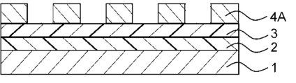
- FIG. 1A is a schematic cross-sectional view for explaining one embodiment of a method for manufacturing a semiconductor device (part 1).
- FIG. 1B is a schematic cross-sectional view for explaining one embodiment of a method for manufacturing a semiconductor element (part 2).
- FIG. 1C is a schematic cross-sectional view for explaining one embodiment of a method for manufacturing a semiconductor element (part 3).
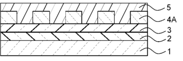
- FIG. 1D is a schematic cross-sectional view for explaining one embodiment of a method for manufacturing a semiconductor element (part 4).
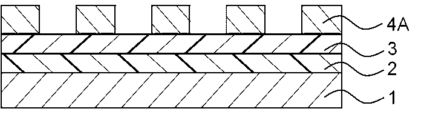
- FIG. 1E is a schematic cross-sectional view for explaining one embodiment of a method for manufacturing a semiconductor element (part 5).
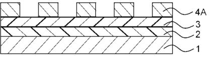
- FIG. 2 is a schematic cross-sectional view showing one embodiment of an organic film between resist patterns.
- FIG. 3A is a schematic cross-sectional view for explaining another embodiment of the method for manufacturing a semiconductor element (part 1).
- FIG. 3B is a schematic cross-sectional view for explaining another embodiment of the method for manufacturing a semiconductor element (part 2).
- FIG. 3C is a schematic cross-sectional view for explaining another embodiment of the method for manufacturing a semiconductor element (part 3).
- FIG. 3D is a schematic cross-sectional view for explaining another embodiment of the method for manufacturing a semiconductor element (part 4).
- the composition for forming an organic film of the present invention is a composition for forming an organic film that is used for forming an organic film that is formed between resist patterns formed from a metal-containing resist film and is then removed.
- the organic film-forming composition contains organic film-constituting components and a solvent.
- the present inventors have found that when a resist pattern is formed from a metal-containing resist film, the resist pattern is likely to collapse after development.
- drying is carried out after development to remove the developer.
- an organic film is formed between the resist patterns after development and then the organic film is removed, thereby preventing the resist pattern from collapsing, and have completed the present invention.
- the present inventors believe that the resist pattern collapse occurs due to the effect of capillary force of the developer during drying to remove the developer.
- WO 2012/128251 discloses a developer used in a lithography process, the developer containing a polymer for forming a dry etching mask and an organic solvent (see, for example, claim 1).
- the technical concept of this developer is clearly different from that of the present invention in that the developer is used to form a reverse pattern using the polymer contained therein.
- JP 2011-33842 A discloses a processing liquid containing an organic solvent-soluble resin and an organic solvent, which is used for forming a pattern using a chemically amplified resist composition (see, for example, claim 1).
- the organic solvent-soluble resin promotes the penetration of the developer or rinse solution into the resist composition and contributes to improving the dissolution rate.
- a metal-containing resist film is used as the resist film. Since resins and metal-containing resist films are usually not compatible with each other, when the resist film is a metal-containing resist film, it is not expected that the organic solvent-soluble resin will promote the penetration of the developer or rinse solution into the resist composition.
- the technical idea of the invention described in JP 2011-33842 A and the present invention are clearly different.
- the metal-containing resist film is not particularly limited, but preferably contains at least one of the following elements: Si, Ge, Sn, Ti, Zr, Hf, Al, and Co.
- the organic film-forming composition is preferably used to prevent the resist pattern from collapsing.
- composition for forming an organic film for example, also serves as a developer when forming a resist pattern.
- the method for removing the organic film is not particularly limited, and examples thereof include methods for removing organic films used in semiconductor lithography processes.
- Methods for removing the organic film include, for example, dry etching, wet etching (e.g., decomposition and removal with an acidic solution), radiation etching, high-temperature baking, dissolution and removal using a solvent, ozone treatment, etc. These can be used alone or in combination of two or more.
- Organic film constituent components are not particularly limited, and examples thereof include low molecular weight compounds, polymers, crosslinking agents, surfactants, curing catalysts, fillers, and other additives.
- An organic film constituent component is a component that is present in the organic film either as is or while reacting with other components when an organic film is formed from the composition for forming an organic film, and can be said to be a component other than the solvent in the composition for forming an organic film.
- the organic film constituent components are not particularly limited as long as they contain an organic component, and do not necessarily have to be entirely composed of organic components, and may contain, for example, an inorganic component.
- the organic film component preferably contains a polymer (A).
- the polymer (A) is not particularly limited.
- the polymer (A) include addition polymerization polymers and condensation polymerization polymers such as polyester, polystyrene, polyimide, acrylic polymer, methacrylic polymer, polyvinyl ether, phenol novolak, naphthol novolak, polyether, polyamide, and polycarbonate.
- the polymer (A) may be, for example, a polymer (A1) or a polymer (A2) described below.
- the polymer (A) is not, for example, a polysiloxane.
- the polymer (A) may be a homopolymer or a copolymer.
- the weight average molecular weight of the polymer (A) is not particularly limited, but is preferably from 1,000 to 200,000, more preferably from 1,500 to 150,000, and particularly preferably from 2,000 to 100,000.
- the weight average molecular weight is a molecular weight obtained by GPC (Gel Permeation Chromatography) analysis in terms of polystyrene.
- the polymer (A) is preferably not water-soluble.
- water-soluble means that 5 g or more of the target substance (e.g., a polymer) dissolves in 100 g of water at 25°C.
- not water-soluble means that less than 5 g of the target substance (e.g., a polymer) dissolves in 100 g of water at 25°C.
- the above-mentioned "soluble” means that no precipitate is observed visually after leaving the solution after dissolving the target substance for 1 hour at a temperature of 20 to 30°C under air. Note that none of the polymers synthesized in Synthesis Examples 1 to 4 in the examples of this specification are water-soluble.
- the polymer (A) is, for example, a polymer (A1) having a ring structure.
- the polymer (A1) is, for example, a polymer (A1-1) having a ring structure in the main chain.
- the polymer (A1) is, for example, a polymer (A1-2) having a ring structure in the side chain.
- the polymer (A1-1) having a ring structure in the main chain may have the ring structure only in the main chain, or may have a ring structure also in a side chain.
- the polymer (A1-2) having a ring structure in the side chain may have the ring structure only in the side chain, or may have the ring structure also in the main chain.
- the main chain refers to, for example, the part of a polymer that is made up of the longest chain of atoms.
- At least one of the ring structures in the main chain of the polymer (A1-1) is, for example, a monocyclic aliphatic ring. At least one of the ring structures in the main chain of the polymer (A1-1) is, for example, a heterocycle. Examples of heteroatoms constituting the heterocycle include an oxygen atom and a nitrogen atom. Examples of the heterocycle include an isocyanurate ring and a barbituric acid ring. At least one of the ring structures in the side chain of the polymer (A1-2) is, for example, a heterocycle. Examples of heteroatoms constituting the heterocycle include an oxygen atom and a nitrogen atom. Examples of the heterocycle include a 5- to 7-membered ring. At least one of the ring structures in the side chains of the polymer (A1-2) is, for example, a lactone ring.
- the polymer (A1-1) is preferably a polymer (X) having a repeating unit represented by the following formula (X):
- T represents a group having a monocyclic aliphatic ring that constitutes the main chain of the polymer (X).
- Q represents a divalent linking group.
- Ar represents an aromatic group which may have a substituent.
- the polymer (X) may have repeating units represented by two or more types of formula (X) in which Ar is different.
- Examples of monocyclic aliphatic rings include cycloalkane rings having 4 to 10 carbon atoms. Among these, cyclohexane rings are preferred.
- the monocyclic aliphatic ring may have a substituent other than -Q-Ar in formula (X).
- substituents include an alkyl group having 1 to 10 carbon atoms, an aryl group having 6 to 20 carbon atoms, a halogen atom, a nitro group, and an amino group.
- alkyl groups having 1 to 10 carbon atoms include methyl, ethyl, n-propyl, isopropyl, cyclopropyl, n-butyl, isobutyl, sec-butyl, tert-butyl, cyclobutyl, 1-methylcyclopropyl, 2-methylcyclopropyl, n-pentyl, 1-methyln-butyl, 2-methyln-butyl, 3-methyln-butyl, 1,1-dimethyln-propyl, 1,2-dimethyln-propyl, 2,2-dimethyln-propyl, 1-ethyln-propyl, cyclopentyl, 1-methylcyclopropyl, n-butyl, 2-methylcyclobutyl, 3-methylcyclobutyl, 1,2-dimethylcyclopropyl, 2,3-dimethylcyclopropyl, 1-ethylcyclopropyl, 2-ethylcyclopropyl,
- aryl groups having 6 to 20 carbon atoms include phenyl, o-methylphenyl, m-methylphenyl, p-methylphenyl, o-chlorophenyl, m-chlorophenyl, p-chlorophenyl, o-fluorophenyl, p-fluorophenyl, o-methoxyphenyl, p-methoxyphenyl, p-nitrophenyl, p-cyanophenyl, ⁇ -naphthyl, ⁇ -naphthyl, o-biphenylyl, m-biphenylyl, p-biphenylyl, 1-anthryl, 2-anthryl, 9-anthryl, 1-phenanthryl, 2-phenanthryl, 3-phenanthryl, 4-phenanthryl, and 9-phenanthryl.
- halogen atoms include fluorine atoms, chlorine atoms, bromine atoms, and iodine atoms.
- the repeating unit represented by formula (X) is preferably a repeating unit represented by the following formula (Xa):
- R 1 represents a hydrogen atom, an alkyl group having 1 to 10 carbon atoms, an aryl group having 6 to 20 carbon atoms, a halogen atom, a nitro group, or an amino group.
- Q represents a divalent linking group.
- Ar represents an aromatic group which may have a substituent.
- the aromatic ring in the aromatic group of Ar in formula (X) and formula (Xa) may be an aromatic cyclic hydrogen ring or an aromatic heterocyclic ring.
- the aromatic ring may be a monocyclic ring or a condensed ring.
- the aromatic hydrocarbon ring include a benzene ring, a naphthalene ring, and an anthracene ring.
- Examples of the substituents that Ar in formula (X) and formula (Xa) may have include an alkyl group having 1 to 10 carbon atoms, an alkoxy group having 1 to 10 carbon atoms, a hydroxy group, a halogen atom, a nitro group, an amino group, etc.
- the number of atoms constituting the divalent linking group in Q in formula (X) and formula (Xa) can be, for example, 1 to 20.
- Q examples include the following linking group (Qa).
- *1 represents a bond bonding to the monocyclic aliphatic ring.
- *2 represents a bond bonding to the aromatic ring.
- the polymer (X) is, for example, a reaction product between a polymer (X1) having a repeating unit represented by the following formula (X1) and an aromatic carboxylic acid (X2).
- R 1 represents a hydrogen atom, an alkyl group having 1 to 10 carbon atoms, an aryl group having 6 to 20 carbon atoms, a halogen atom, a nitro group, or an amino group.
- the polymer having the repeating unit represented by formula (X1) may be a commercially available product.
- EHPE3150 manufactured by Daicel Chemical Industries, Ltd.
- Daicel Chemical Industries, Ltd. may be used.
- aromatic carboxylic acid (X2) examples include monocyclic aromatic carboxylic acids and condensed ring aromatic carboxylic acids.
- An example of the monocyclic aromatic carboxylic acid is benzoic acid.
- Examples of the fused ring aromatic carboxylic acid include naphthalene carboxylic acid and anthracene carboxylic acid.
- Examples of the polymer (X) include the following polymers (X-1) to (X-12).
- the following polymers have two or three types of repeating units.
- polymer (X) examples include the polymers described in WO 2011/021555.
- the contents of WO 2011/021555 are incorporated herein by reference to the same extent as if fully set forth.
- the weight average molecular weight of polymer (X) is not particularly limited, but is preferably 1,000 to 15,000, more preferably 1,500 to 10,000, and particularly preferably 2,000 to 7,000.
- the polymer (A1-1) is preferably a polymer (Y) having a repeating unit represented by the following formula (Y):
- a 1 , A 2 , A 3 , A 4 , A 5 , and A 6 each represent a hydrogen atom, a methyl group, or an ethyl group.
- X1 represents the following formula (Y2), the following formula (Y3), the following formula (Y4), or the following formula (Y0).
- Q represents the following formula (Y5) or the following formula (Y6):
- R 1 and R 2 each represent a hydrogen atom, a halogen atom, an alkyl group having 1 to 6 carbon atoms, an alkenyl group having 3 to 6 carbon atoms, a benzyl group, or a phenyl group, and the alkyl group having 1 to 6 carbon atoms, the alkenyl group having 3 to 6 carbon atoms, the benzyl group, and the phenyl group may be substituted with a group selected from the group consisting of an alkyl group having 1 to 6 carbon atoms, a halogen atom, an alkoxy group having 1 to 6 carbon atoms, a nitro group, a cyano group, a hydroxyl group, a carboxyl group, and an alkylthio group having 1 to 6 carbon atoms.
- R 1 and R 2 may be bonded to each other to form a ring having 3 to 6 carbon atoms.
- R3 represents a halogen atom, an alkyl group having 1 to 6 carbon atoms, an alkenyl group having 3 to 6 carbon atoms, a benzyl group, or a phenyl group, and the phenyl group may be substituted with a group selected from the group consisting of an alkyl group having 1 to 6 carbon atoms, a halogen atom, an alkoxy group having 1 to 6 carbon atoms, a nitro group, a cyano group, a hydroxy group, and an alkylthio group having 1 to 6 carbon atoms.
- * represents a bond.
- *1 represents a bond bonded to a carbon atom.
- *2 represents a bond bonded to a nitrogen atom.
- Q1 represents an alkylene group having 1 to 10 carbon atoms, a phenylene group, a naphthylene group, or an anthrylene group
- the alkylene group, the phenylene group, the naphthylene group, and the anthrylene group may each be substituted with an alkyl group having 1 to 6 carbon atoms, a carbonyloxyalkyl group having 2 to 7 carbon atoms, a halogen atom, an alkoxy group having 1 to 6 carbon atoms, a phenyl group, a nitro group, a cyano group, a hydroxy group, an alkylthio group having 1 to 6 carbon atoms, a group having a disulfide group, a carboxyl group, or a group consisting of a combination thereof.
- n1 and n2 each represent 0 or 1.
- X2 represents the formula (Y2), the formula (Y3), or the formula (Y0). * represents
- repeating unit represented by formula (Y) examples include repeating units represented by the following formulas (Y-1) to (Y-20).
- R is an alcohol residue (an organic group other than the hydroxyl group of an alcohol), and this R represents an alkyl group, an ether group, or a combination thereof.
- R include an alkyl group, an alkoxyalkyl group, etc.
- polymer (Y) examples include the polymers described in WO 2013/018802. The contents of WO 2013/018802 are incorporated herein by reference to the same extent as if fully set forth.
- the weight average molecular weight of polymer (Y) is not particularly limited, but is preferably 1,000 to 30,000, more preferably 2,000 to 20,000, and particularly preferably 3,000 to 15,000.
- the polymer (A1-2) is preferably a polymer (Z) having a repeating unit represented by the following formula (Z):
- Q represents a divalent linking group.
- R 1 represents a substituted or unsubstituted trivalent hydrocarbon group having 3 or 4 carbon atoms.
- P represents a bonding group constituting the main chain.
- R2 represents a hydrogen atom, a methyl group, or a halogen atom.
- the repeating unit represented by formula (Z) is preferably a repeating unit represented by the following formula (Za).
- R2 represents a hydrogen atom, a methyl group or a halogen atom.
- L represents the following formula (L-1) or formula (L-2): (In formula (L-1) and formula (L-2), * represents a bond.)
- the polymer (Z) may have a repeating unit represented by the following formula (Z-2).
- R 3 represents a hydrogen atom, a methyl group or a halogen atom.
- R4 represents a hydrogen atom, a substituted or unsubstituted alkyl group having 1 to 10 carbon atoms, a substituted or unsubstituted aralkyl group, a substituted or unsubstituted carbocyclic aromatic group, or a substituted or unsubstituted heterocyclic aromatic group.
- Examples of the repeating unit represented by formula (Z-2) include a repeating unit represented by the following formula (Z-2-1) and a repeating unit represented by formula (Z-2-2).
- R 3 represents a hydrogen atom, a methyl group or a halogen atom.
- R 4a represents an alkyl group having 1 to 4 carbon atoms substituted with a hydroxy group.
- R 4b represents a substituted or unsubstituted carbocyclic aromatic group.
- Examples of the substituted or unsubstituted alkyl group having 1 to 10 carbon atoms for R 4 in formula (Z-2) include an alkyl group having 1 to 10 carbon atoms and an alkyl group having 1 to 4 carbon atoms substituted with a hydroxy group.
- Examples of the substituted or unsubstituted carbocyclic aromatic group in R 4 in formula (Z-2) and R 4b in formula (Z-2-2) include a phenyl group, a benzyl group, a naphthyl group, an anthryl group, and an anthrylmethyl group.
- Examples of the alkyl group having 1 to 4 carbon atoms substituted with a hydroxy group include a 2-hydroxyethyl group and a 2-hydroxypropyl group.
- the polymer (Z) may have other repeating units.
- monomers from which the other repeating units are derived include acrylamides, methacrylamides, allyl compounds, vinyl ethers, vinyl esters, styrenes, and crotonates.
- acrylamides include acrylamide, N-alkylacrylamide, N-arylacrylamide, N,N-dialkylacrylamide, N,N-diarylacrylamide, N-methyl-N-phenylacrylamide, and N-2-acetamidoethyl-N-acetylacrylamide.
- methacrylamides include methacrylamide, N-alkylmethacrylamide, N-arylmethacrylamide, N,N-dialkylmethacrylamide, N,N-diarylmethacrylamide, N-methyl-N-phenylmethacrylamide, and N-ethyl-N-phenylmethacrylamide.
- vinyl ethers include alkyl vinyl ethers and vinyl aryl ethers.
- vinyl esters include vinyl butyrate, vinyl isobutyrate, and vinyl trimethyl acetate.
- styrenes include styrene, alkylstyrene, alkoxystyrene, halogenated styrene, and carboxystyrene.
- crotonates include alkyl crotonates such as butyl crotonate, hexyl crotonate, and glycerin monocrotonate. Further examples include dialkyl itaconates, dialkyl esters or monoalkyl esters of maleic acid or fumaric acid, crotonic acid, itaconic acid, maleic anhydride, acrylonitrile, methacrylonitrile, maleironitrile, and the like.
- Polymer (Z) may be any of the polymers described in WO 03/017002.
- the contents of WO 03/017002 are incorporated herein by reference to the same extent as if expressly set forth in their entirety.
- the weight average molecular weight of the polymer (Z) is not particularly limited, but is preferably 10,000 to 200,000, more preferably 30,000 to 150,000, and particularly preferably 50,000 to 100,000.
- the polymer (A) is preferably a polymer (A2) having a repeating unit represented by the following formula (Q).
- R 11 represents an alkyl group having 1 to 4 carbon atoms.
- R 12 represents a hydrogen atom, a methyl group, or a halogen atom.
- the polymer (A2) may be a homopolymer or a copolymer.
- the polymer (A2) is a homopolymer
- the polymer (A2) is preferably, for example, polymethyl methacrylate.
- the polymer (A2) when the polymer (A2) is a copolymer, the polymer (A2) may have a repeating unit represented by formula (Z-2) as a repeating unit other than the repeating unit represented by formula (Q). Furthermore, when the polymer (A2) is a copolymer, the polymer (A2) may have repeating units derived from acrylamides, methacrylamides, allyl compounds, vinyl ethers, vinyl esters, styrenes, crotonates, etc.
- the weight average molecular weight of polymer (Q) is not particularly limited, but is preferably 1,000 to 30,000, more preferably 2,000 to 20,000, and particularly preferably 3,000 to 15,000.
- the content of polymer (A) in the organic film-forming composition is not particularly limited, but is preferably 30% by mass to 100% by mass, more preferably 50% by mass to 100% by mass, and particularly preferably 70% by mass to 100% by mass, based on the organic film constituents.
- the crosslinking agent is not particularly limited.
- the crosslinking agent has a structure different from that of the polymer (A).
- an aminoplast crosslinking agent or a phenoplast crosslinking agent is preferred.
- Aminoplast crosslinking agents are addition condensation products of a compound having an amino group, such as melamine or guanamine, and formaldehyde.
- the phenoplast crosslinking agent is an addition condensation product of a compound having a phenolic hydroxy group and formaldehyde.
- the crosslinking agent may, for example, be a compound having two or more of the following structures.
- R 101 represents a hydrogen atom, an alkyl group having 1 to 4 carbon atoms, or an alkoxyalkyl group having 2 to 6 carbon atoms. * represents a bond.
- the bond is, for example, bonded to a nitrogen atom or a carbon atom constituting an aromatic hydrocarbon ring.
- R 101 is preferably a hydrogen atom, a methyl group, an ethyl group or a group represented by the following structure.
- R 102 represents a hydrogen atom, a methyl group, or an ethyl group. * represents a bond.
- Preferred crosslinking agents are melamine compounds, guanamine compounds, glycoluril compounds, urea compounds, and compounds having a phenolic hydroxyl group. These can be used alone or in combination of two or more.
- melamine compounds include hexamethylol melamine, hexamethoxymethyl melamine, compounds in which 1 to 6 methylol groups of hexamethylol melamine are methoxymethylated or mixtures thereof, hexamethoxyethyl melamine, hexaacyloxymethyl melamine, compounds in which 1 to 6 methylol groups of hexamethylol melamine are acyloxymethylated or mixtures thereof, etc.
- guanamine compounds include tetramethylol guanamine, tetramethoxymethyl guanamine, compounds in which one to four methylol groups of tetramethylol guanamine are methoxymethylated or mixtures thereof, tetramethoxyethyl guanamine, tetraacyloxyguanamine, compounds in which one to four methylol groups of tetramethylol guanamine are acyloxymethylated or mixtures thereof, etc.
- glycoluril compounds include tetramethylol glycoluril, tetramethoxy glycoluril, tetramethoxymethyl glycoluril, compounds in which one to four methylol groups of tetramethylol glycoluril are methoxymethylated or mixtures thereof, and compounds in which one to four methylol groups of tetramethylol glycoluril are acyloxymethylated or mixtures thereof.
- the glycoluril compound may be, for example, a glycoluril derivative represented by the following formula (1E).
- the four R 1s each independently represent a methyl group or an ethyl group
- R 2 and R 3 each independently represent a hydrogen atom, an alkyl group having 1 to 4 carbon atoms, or a phenyl group.
- glycoluril derivative represented by formula (1E) examples include compounds represented by formulas (1E-1) to (1E-6) below.
- the glycoluril derivative represented by formula (1E) can be obtained, for example, by reacting a glycoluril derivative represented by the following formula (2E) with at least one compound represented by the following formula (3d).
- R2 and R3 each independently represent a hydrogen atom, an alkyl group having 1 to 4 carbon atoms, or a phenyl group, and R4 each independently represent an alkyl group having 1 to 4 carbon atoms.
- R 1 represents a methyl group or an ethyl group.
- glycoluril derivative represented by formula (2E) examples include compounds represented by the following formulae (2E-1) to (2E-4).
- Examples of the compound represented by formula (3d) include compounds represented by the following formulae (3d-1) and (3d-2).
- urea compounds include tetramethylol urea, tetramethoxymethyl urea, tetramethylol urea in which one to four methylol groups are methoxymethylated or mixtures thereof, tetramethoxyethyl urea, etc.
- Examples of the compound having a phenolic hydroxy group include compounds represented by the following formula (G-1) or (G-2).
- Q1 represents a single bond or an m1-valent organic group.
- R 1 and R 4 each represent an alkyl group having 2 to 10 carbon atoms, or an alkyl group having 2 to 10 carbon atoms and an alkoxy group having 1 to 10 carbon atoms.
- R2 and R5 each represent a hydrogen atom or a methyl group.
- R3 and R6 each represent an alkyl group having 1 to 10 carbon atoms or an aryl group having 6 to 40 carbon atoms.
- n1 is an integer satisfying 1 ⁇ n1 ⁇ 3, n2 is an integer satisfying 2 ⁇ n2 ⁇ 5, n3 is an integer satisfying 0 ⁇ n3 ⁇ 3, n4 is an integer satisfying 0 ⁇ n4 ⁇ 3, and 3 ⁇ ( n1 + n2 + n3 + n4 ) ⁇ 6.
- n5 is an integer satisfying 1 ⁇ n5 ⁇ 3, n6 is an integer satisfying 1 ⁇ n6 ⁇ 4, n7 is an integer satisfying 0 ⁇ n7 ⁇ 3, n8 is an integer satisfying 0 ⁇ n8 ⁇ 3, and 2 ⁇ ( n5 + n6 + n7 + n8 ) ⁇ 5.
- m1 represents an integer from 2 to 10.
- Examples of the compound having a phenolic hydroxy group include the compounds represented by the following formula (G-3) or (G-4).
- the compound represented by formula (G-1) or formula (G-2) may be obtained by reacting a compound represented by the following formula (G-3) or formula (G-4) with a hydroxyl group-containing ether compound or an alcohol having 2 to 10 carbon atoms.
- Q2 represents a single bond or an m2-valent organic group.
- R 8 , R 9 , R 11 and R 12 each represent a hydrogen atom or a methyl group.
- R7 and R10 each represent an alkyl group having 1 to 10 carbon atoms or an aryl group having 6 to 40 carbon atoms.
- n9 is an integer satisfying 1 ⁇ n9 ⁇ 3, n10 is an integer satisfying 2 ⁇ n10 ⁇ 5, n11 is an integer satisfying 0 ⁇ n11 ⁇ 3, n12 is an integer satisfying 0 ⁇ n12 ⁇ 3, and 3 ⁇ ( n9 + n10 + n11 + n12 ) ⁇ 6.
- n13 is an integer satisfying 1 ⁇ n13 ⁇ 3, n14 is an integer satisfying 1 ⁇ n14 ⁇ 4, n15 is an integer satisfying 0 ⁇ n15 ⁇ 3, n16 is an integer satisfying 0 ⁇ n16 ⁇ 3, and 2 ⁇ ( n13 + n14 + n15 + n16 ) ⁇ 5.
- m2 represents an integer from 2 to 10.
- the m2-valent organic group for Q2 includes, for example, an m2-valent organic group having 1 to 4 carbon atoms.
- Examples of the compound represented by formula (G-1) or formula (G-2) include the following compounds.
- Examples of the compound represented by formula (G-3) or formula (G-4) include the following compounds.
- the above compound is available as a product of Asahi Yukizai Kogyo Co., Ltd. and Honshu Chemical Industry Co., Ltd.
- An example of the product is TMOM-BP, a product name of Asahi Yukizai Kogyo Co., Ltd.
- glycoluril compounds are preferred, specifically tetramethylol glycoluril, tetramethoxy glycoluril, tetramethoxymethyl glycoluril, a compound in which one to four methylol groups of tetramethylol glycoluril are methoxymethylated or a mixture thereof, and a compound in which one to four methylol groups of tetramethylol glycoluril are acyloxymethylated or a mixture thereof, with tetramethoxymethyl glycoluril being more preferred.
- the molecular weight of the crosslinking agent is not particularly limited, but is preferably 500 or less.
- the content of the crosslinking agent in the organic film-forming composition is not particularly limited, but is, for example, 1% by mass to 70% by mass, and preferably 5% by mass to 60% by mass, relative to the polymer (A).
- the curing catalyst as an organic film-constituting component contained as an optional component in the organic film-forming composition may be either a thermal acid generator or a photoacid generator, but it is preferable to use a thermal acid generator.
- the thermal acid generator include sulfonic acid compounds and carboxylic acid compounds such as p-toluenesulfonic acid, trifluoromethanesulfonic acid, pyridinium p-toluenesulfonate (pyridinium p-toluenesulfonic acid), pyridinium phenolsulfonic acid, pyridinium p-hydroxybenzenesulfonic acid (pyridinium p-phenolsulfonate salt), pyridinium trifluoromethanesulfonic acid, salicylic acid, camphorsulfonic acid, 5-sulfosalicylic acid, 4-chlorobenzenesulfonic acid, 4-hydroxybenzenesulfonic acid, 4-hydroxy
- photoacid generators examples include onium salt compounds, sulfonimide compounds, and disulfonyldiazomethane compounds.
- onium salt compounds include iodonium salt compounds such as diphenyliodonium hexafluorophosphate, diphenyliodonium trifluoromethanesulfonate, diphenyliodonium nonafluoronormal butanesulfonate, diphenyliodonium perfluoronormal octanesulfonate, diphenyliodonium camphorsulfonate, bis(4-tert-butylphenyl)iodonium camphorsulfonate, and bis(4-tert-butylphenyl)iodonium trifluoromethanesulfonate, and sulfonium salt compounds such as triphenylsulfonium hexafluoroantimonate, triphenylsulfonium nonafluoronormal butanesulfonate, triphenylsulfonium camphorsulfonate, and triphenylsulfonium triflu
- sulfonimide compounds include N-(trifluoromethanesulfonyloxy)succinimide, N-(nonafluoronormalbutanesulfonyloxy)succinimide, N-(camphorsulfonyloxy)succinimide, and N-(trifluoromethanesulfonyloxy)naphthalimide.
- disulfonyldiazomethane compounds include bis(trifluoromethylsulfonyl)diazomethane, bis(cyclohexylsulfonyl)diazomethane, bis(phenylsulfonyl)diazomethane, bis(p-toluenesulfonyl)diazomethane, bis(2,4-dimethylbenzenesulfonyl)diazomethane, and methylsulfonyl-p-toluenesulfonyldiazomethane.
- the content of the curing catalyst relative to the crosslinking agent is, for example, 0.1% by mass to 50% by mass, and preferably 1% by mass to 30% by mass.
- a surfactant can be further added as an organic film-forming component to the composition.
- surfactant examples include polyoxyethylene alkyl ethers such as polyoxyethylene lauryl ether, polyoxyethylene stearyl ether, polyoxyethylene cetyl ether, and polyoxyethylene oleyl ether; polyoxyethylene alkylaryl ethers such as polyoxyethylene octylphenol ether and polyoxyethylene nonylphenol ether; polyoxyethylene-polyoxypropylene block copolymers; sorbitan fatty acid esters such as sorbitan monolaurate, sorbitan monopalmitate, sorbitan monostearate, sorbitan monooleate, sorbitan trioleate, and sorbitan tristearate; polyoxyethylene sorbitan monolaurate, polyoxyethylene sorbitan monopalmitate, sorbitan monostearate, sorbitan monooleate, sorbitan tristearate, and the like; nonionic surfactants such as polyoxyethylene sorbitan fatty acid esters, such as polyoxyethylene sorbitan
- the solvent used in the organic film-forming composition is not particularly limited, but is preferably an organic solvent generally used in chemicals for semiconductor lithography processes. Specifically, ethylene glycol monomethyl ether, ethylene glycol monoethyl ether, methyl cellosolve acetate, ethyl cellosolve acetate, diethylene glycol monomethyl ether, diethylene glycol monoethyl ether, propylene glycol, propylene glycol monomethyl ether, propylene glycol monoethyl ether, propylene glycol monomethyl ether acetate, propylene glycol propyl ether acetate, toluene, xylene, methyl ethyl ketone, methyl isobutyl ketone, cyclopentanone, cyclohexanone, cyclohexane ...
- Examples of the solvent include heptanone, 4-methyl-2-pentanol, methyl 2-hydroxyisobutyrate, ethyl 2-hydroxyisobutyrate, ethyl ethoxyacetate, 2-hydroxyethyl acetate, methyl 3-methoxypropionate, ethyl 3-methoxypropionate, ethyl 3-ethoxypropionate, methyl 3-ethoxypropionate, methyl pyruvate, ethyl pyruvate, ethyl acetate, butyl acetate, ethyl lactate, butyl lactate, 2-heptanone, methoxycyclopentane, anisole, ⁇ -butyrolactone, N-methylpyrrolidone, N,N-dimethylformamide, and N,N-dimethylacetamide. These solvents can be used alone or in combination of two or more.
- propylene glycol monomethyl ether propylene glycol monomethyl ether acetate, ethyl lactate, butyl lactate, and cyclohexanone are preferred.
- Propylene glycol monomethyl ether and propylene glycol monomethyl ether acetate are particularly preferred.
- the solvent preferably does not contain water, in other words, the organic film-forming composition preferably does not contain water.
- the water content in the organic film-forming composition is not particularly limited, but is preferably 0% by mass to 10% by mass, more preferably 0% by mass to 5% by mass, and particularly preferably 0% by mass to 3% by mass.
- the content of the solvent in the organic film-forming composition is not particularly limited, but is preferably 80% by mass to 99.99% by mass, more preferably 85% by mass to 99.9% by mass, and particularly preferably 90% by mass to 99% by mass.
- the content of the organic film constituent components in the organic film-forming composition is not particularly limited, but is preferably 0.01% by mass to 20% by mass, more preferably 0.1% by mass to 15% by mass, and particularly preferably 1% by mass to 10% by mass.
- An example of a method for manufacturing a semiconductor element of the present invention includes an irradiation step, a resist pattern forming step, an organic film forming step, and an organic film removing step.
- the example method for manufacturing a semiconductor device may include other steps.
- the irradiation step is a step of irradiating the metal-containing resist film with light or an electron beam.
- the metal-containing resist film is not particularly limited, but preferably contains at least one of the following elements: Si, Ge, Sn, Ti, Zr, Hf, Al, and Co.
- the metal-containing resist film is formed from, for example, a metal-containing resist.
- Metal-containing resists are also called metal oxide resists (MOR), and a representative example is a tin oxide-based resist.
- MOR metal oxide resists
- metal oxide resist materials include coating compositions comprising metal oxo-hydroxo networks having organic ligands via metal carbon bonds and/or metal carboxylate bonds, as described in JP 2019-113855 A.
- An example of a metal-containing resist uses a peroxo ligand as a radiation-sensitive stabilizing ligand.
- Peroxo-based metal oxo-hydroxo compounds are described in detail in, for example, the patent documents described in paragraph [0011] of Publication 2019-532489. Examples of such patent documents include U.S. Pat.
- metal-containing resists include those described in JP 2011-253185 A, WO 2015/026482, WO 2016/065120, WO 2017/066319, WO 2017/156388, WO 2018/031896, JP 2020-122959 A, JP 2020-122960 A, WO 2019/099981, WO 2019/199467, WO 2019/195522, WO 2019/195522, WO 2020/210660, WO 2021/011367, and WO 2021/016229. The contents of these are incorporated herein to the same extent as if fully set forth.
- the method for forming a metal-containing resist film from a metal-containing resist is not particularly limited, and examples include a method in which a coating-type resist material (composition for forming a metal-containing resist film), which is a metal-containing resist, is coated and baked.
- the metal-containing resist film may also be formed by vapor deposition.
- methods for forming a metal-containing resist film by vapor deposition include the method described in JP 2017-116923 A.
- the contents of JP 2017-116923 A are incorporated herein by reference to the same extent as if fully set forth herein.
- the metal-containing resist film of the present invention is referred to as a metal oxide-containing film.
- the thickness of the metal-containing resist film is, for example, 5 nm to 10,000 nm, or 5 nm to 1,000 nm, or 5 nm to 40 nm.
- the metal-containing resist film is formed, for example, on a substrate, a resist underlayer film, etc.
- Substrates include, for example, substrates used in the manufacture of precision integrated circuit elements.
- substrates include semiconductor substrates such as silicon wafers coated with a silicon oxide film, silicon nitride film, or silicon oxynitride film, silicon nitride substrates, quartz substrates, glass substrates (including alkali-free glass, low-alkali glass, and crystallized glass), glass substrates on which an ITO (indium tin oxide) film or an IZO (indium zinc oxide) film is formed, plastic (polyimide, PET, etc.) substrates, substrates coated with low dielectric constant materials (low-k materials), flexible substrates, etc.
- semiconductor substrates such as silicon wafers coated with a silicon oxide film, silicon nitride film, or silicon oxynitride film, silicon nitride substrates, quartz substrates, glass substrates (including alkali-free glass, low-alkali glass, and crystallized glass), glass substrates on which an ITO (indium t
- the resist underlayer film is not particularly limited, and for example, a known resist underlayer film can be used.
- Examples of the resist underlayer film include an organic underlayer film and a silicon-containing resist underlayer film.
- the resist film may be formed directly on the substrate, or may be formed on the resist underlayer film of the substrate on which the resist underlayer film has been formed.
- the resist underlayer film may be a single layer or multiple layers.
- a two-layer resist underlayer film may be present between the substrate and the resist film.
- An example of a two-layer resist underlayer film is a two-layer resist underlayer film consisting of an organic underlayer film and a silicon-containing resist underlayer film.
- the thickness of the resist underlayer film is, for example, 10 nm to 1,000 nm, or 20 nm to 500 nm, or 50 nm to 300 nm, or 100 nm to 200 nm, or 10 to 150 nm.
- Examples of the light or electron beam irradiated to the metal-containing resist film include KrF excimer laser (wavelength 248 nm), ArF excimer laser (wavelength 193 nm), F2 excimer laser (wavelength 157 nm), EUV (wavelength 13.5 nm), and electron beam.
- the amount of light or electron beam irradiated onto the metal-containing resist film is not particularly limited.
- a post-exposure bake can be performed as necessary.
- the post-exposure bake is performed under conditions appropriately selected from, for example, a heating temperature of 70°C to 250°C and a heating time of 0.3 minutes to 10 minutes.
- the resist pattern forming step is a step in which a developer is brought into contact with the metal-containing resist film that has been irradiated with light or an electron beam to obtain a resist pattern.
- An organic solvent can be used as the developer, and development is carried out with the developer (solvent) after irradiation with light or electron beams.
- the developer solvent
- development is carried out with the developer (solvent) after irradiation with light or electron beams.
- Examples of developing solutions include methyl acetate, butyl acetate, ethyl acetate, isopropyl acetate, amyl acetate, isoamyl acetate, ethyl methoxyacetate, ethyl ethoxyacetate, propylene glycol monomethyl ether acetate, ethylene glycol monoethyl ether acetate, ethylene glycol monopropyl ether acetate, ethylene glycol monobutyl ether acetate, ethylene glycol monophenyl ether acetate, diethylene glycol monomethyl ether acetate, diethylene glycol monopropyl ether acetate, diethylene glycol monoethyl ether acetate, diethylene glycol monophenyl ether acetate, diethylene glycol monobutyl ether acetate, diethylene glycol monoethyl ether acetate, 2-methoxybutyl acetate, 3-methoxybutyl acetate, 3-meth
- spin development by spin coating can be mentioned.
- the rotation speed during spin development is not particularly limited, but can be, for example, 500 rpm (rotations per minute) to 1500 rpm.
- the time for spin development is not particularly limited, but can be, for example, 30 seconds to 120 seconds.
- the resist pattern forming process development is carried out so that the resist pattern in contact with the developer does not dry.
- drying is performed after development to remove the developer, but in the present invention, the developer is not dried because drying the developer would cause the resist pattern to collapse.
- spin drying is generally performed after spin development, but in the present invention, spin drying is not performed.
- the organic film formation step is performed without spin drying.
- the rotation speed during spin drying is not particularly limited, but may be, for example, 2000 rpm to 3000 rpm
- the time for spin drying is not particularly limited, but may be, for example, 10 seconds to 90 seconds.
- the organic film forming step is a step of applying the organic film forming composition of the present invention onto a resist pattern without drying the resist pattern in contact with the developer, thereby forming an organic film between the resist patterns.
- the method for forming the organic film is not particularly limited, but for example, spin coating is an example.
- the rotation speed during spin coating is not particularly limited, but for example, 500 rpm to 1500 rpm is an example.
- the time for spin coating is not particularly limited, but for example, 30 seconds to 120 seconds is an example.
- the organic film formed by the organic film formation process may be formed only between the resist patterns. Also, the organic film may be formed on the resist patterns in addition to between the resist patterns.
- the thickness of the organic film to be formed is not particularly limited, and is set to an appropriate thickness depending on, for example, the thickness of the metal-containing resist film.
- the thickness of the organic film is, for example, in the range of 0.5 to 1.5 times the thickness of the metal-containing resist film.
- the organic film removing step is not particularly limited as long as it is capable of removing the organic film.
- Methods for removing the organic film include, for example, dry etching, wet etching (e.g., decomposition and removal with an acidic solution), radiation etching, high-temperature baking, dissolution and removal using a solvent, ozone treatment, etc. These can be used alone or in combination of two or more.
- the temperature in the high-temperature firing may be, for example, 200° C. to 300° C.
- the firing time in the high-temperature firing may be, for example, 1 minute or longer.
- the atmosphere in the high-temperature firing may be, for example, air.
- the solvent used for dissolving and removing the resist include the organic solvents mentioned in the description of the developer (organic solvent) used in the resist pattern formation step described above.
- gases used in dry etching include tetrafluoromethane (CF 4 ), perfluorocyclobutane (C 4 F 8 ), perfluoropropane (C 3 F 8 ), trifluoromethane, carbon monoxide, argon, oxygen, nitrogen, sulfur hexafluoride, difluoromethane, nitrogen trifluoride, chlorine trifluoride, chlorine, trichloroborane, dichloroborane, etc. These may be used alone or in combination of two or more.
- Radiation etching is carried out, for example, by irradiating with ultraviolet light in the presence of oxygen (eg, in the air) or in the presence of an inert gas (eg, nitrogen).
- the organic film is decomposed and removed by ultraviolet light.
- ozone is generated by irradiation with ultraviolet rays (e.g., 100 nm to 400 nm, 185 nm ultraviolet rays).
- ultraviolet rays e.g., 254 nm
- active oxygen is generated. The active oxygen then decomposes the organic film. As a result, the organic film is removed.
- the organic film removal step it is preferable that the organic film is selectively removed.
- the etching speed (etch rate) of the organic film when the organic film is removed is preferably at least twice the etching speed of the metal-containing resist film, more preferably at least 10 times, and particularly preferably at least 20 times.
- the etching speed of the organic film when the organic film is removed is not more than 100 times the etching speed of the metal-containing resist film.
- the resist pattern of the metal-containing resist film (upper layer) thus formed is used as a protective film to remove the resist underlayer film (middle layer), and then the organic underlayer film (lower layer) is removed using a film consisting of the patterned metal-containing resist film and the patterned resist underlayer film (middle layer) as a protective film. Finally, the substrate is processed using the patterned resist underlayer film (middle layer) and the patterned organic underlayer film (lower layer) as protective films.
- the removal (patterning) of the resist underlayer film (middle layer) is performed by dry etching using the pattern of the metal-containing resist film (upper layer) as a protective film, and gases such as tetrafluoromethane (CF 4 ), perfluorocyclobutane (C 4 F 8 ), perfluoropropane (C 3 F 8 ), trifluoromethane, carbon monoxide, argon, oxygen, nitrogen, sulfur hexafluoride, difluoromethane, nitrogen trifluoride, chlorine trifluoride, chlorine, trichloroborane, and dichloroborane can be used. It is preferable to use a halogen-based gas for dry etching of the resist underlayer film.
- gases such as tetrafluoromethane (CF 4 ), perfluorocyclobutane (C 4 F 8 ), perfluoropropane (C 3 F 8 ), trifluoromethane, carbon monoxide, argon
- the metal-containing resist film In dry etching with a halogen-based gas, the metal-containing resist film is basically difficult to remove. In contrast, the resist underlayer film containing a large amount of silicon atoms is quickly removed by the halogen-based gas. Therefore, the reduction in the thickness of the metal-containing resist film caused by dry etching of the resist underlayer film can be suppressed. As a result, the metal-containing resist film can be used as a thin film.
- the dry etching of the resist underlayer film is preferably performed with a fluorine-based gas
- a fluorine-based gas examples include, but are not limited to, tetrafluoromethane (CF 4 ), perfluorocyclobutane (C 4 F 8 ), perfluoropropane (C 3 F 8 ), trifluoromethane, difluoromethane (CH 2 F 2 ), etc.
- the removal (patterning) of the organic underlayer film (lower layer) is preferably performed by dry etching with an oxygen-based gas (oxygen gas, oxygen/carbonyl sulfide (COS) mixed gas, etc.) using the patterned resist underlayer film (middle layer) (and the patterned metal-containing resist film (upper layer) if any remains) as a protective film.
- an oxygen-based gas oxygen gas, oxygen/carbonyl sulfide (COS) mixed gas, etc.
- processing (patterning) of the (semiconductor) substrate which is carried out using the patterned resist underlayer film (intermediate layer) and, if desired, the patterned organic underlayer film (underlayer) as protective films, is preferably carried out by dry etching using a fluorine-based gas.
- fluorine-based gases include tetrafluoromethane (CF 4 ), perfluorocyclobutane (C 4 F 8 ), perfluoropropane (C 3 F 8 ), trifluoromethane, and difluoromethane (CH 2 F 2 ).
- the resist underlayer film may be removed by dry etching or wet etching (wet method). Dry etching of the resist underlayer film is preferably performed using a fluorine-based gas as described in the patterning, such as, but not limited to, tetrafluoromethane (CF 4 ), perfluorocyclobutane (C 4 F 8 ), perfluoropropane (C 3 F 8 ), trifluoromethane, difluoromethane (CH 2 F 2 ), etc.
- a fluorine-based gas as described in the patterning, such as, but not limited to, tetrafluoromethane (CF 4 ), perfluorocyclobutane (C 4 F 8 ), perfluoropropane (C 3 F 8 ), trifluoromethane, difluoromethane (CH 2 F 2 ), etc.
- Examples of chemical solutions used for wet etching of the resist underlayer film include alkaline solutions such as dilute hydrofluoric acid (hydrofluoric acid), buffered hydrofluoric acid (a mixed solution of HF and NH 4 F), an aqueous solution containing hydrochloric acid and hydrogen peroxide (SC-2 chemical solution), an aqueous solution containing sulfuric acid and hydrogen peroxide (SPM chemical solution), an aqueous solution containing hydrofluoric acid and hydrogen peroxide (FPM chemical solution), and an aqueous solution containing ammonia and hydrogen peroxide (SC-1 chemical solution).
- alkaline solutions such as dilute hydrofluoric acid (hydrofluoric acid), buffered hydrofluoric acid (a mixed solution of HF and NH 4 F), an aqueous solution containing hydrochloric acid and hydrogen peroxide (SC-2 chemical solution), an aqueous solution containing sulfuric acid and hydrogen peroxide (SPM chemical solution), an aqueous solution containing hydrofluor
- alkaline solution examples include ammonia hydrogen peroxide (SC-1 solution) obtained by mixing ammonia, hydrogen peroxide, and water, as well as aqueous solutions containing 1 to 99% by mass of ammonia, tetramethylammonium hydroxide (TMAH), tetraethylammonium hydroxide, tetrapropylammonium hydroxide, tetrabutylammonium hydroxide, choline hydroxide, benzyltrimethylammonium hydroxide, benzyltriethylammonium hydroxide, DBU (diazabicyclondecene), DBN (diazabicyclononene), hydroxylamine, 1-butyl-1-methylpyrrolidinium hydroxide, 1-propyl-1-methylpyrrolidinium hydroxide, 1-butyl-1-methylpiperidinium hydroxide, 1-propyl-1-methylpiperidinium hydroxide, mepicato hydroxide, tri
- an organic anti-reflective film can be formed on top of the resist underlayer film before the formation of the metal-containing resist film.
- the anti-reflective film composition used therein and any composition that has been conventionally used in lithography processes can be selected and used, and the anti-reflective film can be formed by conventional methods, such as coating with a spinner or coater and baking.
- the substrate on which the silicon-containing resist underlayer film forming composition for forming the silicon-containing resist underlayer film is applied may have an organic or inorganic anti-reflective film formed on its surface by a CVD method or the like, and the resist underlayer film may be formed on top of it.
- the substrate used may also have an organic or inorganic anti-reflective film formed on its surface by a CVD method or the like.
- the resist underlayer film formed from the composition for forming a silicon-containing resist underlayer film may also absorb light depending on the wavelength of the light used in the lithography process, and in such a case, can function as an anti-reflection film having an effect of preventing light reflected from the substrate.
- the resist underlayer film can also be used as a layer for preventing interaction between the substrate and the metal-containing resist film, a layer having a function of preventing adverse effects on the substrate of materials used in the metal-containing resist film or substances generated during exposure of the metal-containing resist film, a layer having a function of preventing diffusion of substances generated from the substrate during heating and baking into the metal-containing resist film, and a barrier layer for reducing the poisoning effect of the metal-containing resist film due to the dielectric layer of the semiconductor substrate.
- the composition for forming an organic film may also serve as a developer.
- the method for producing a semiconductor element includes an irradiation step, a resist pattern and organic film forming step, and an organic film removing step.
- the irradiation step may be the above-mentioned irradiation step.
- the organic film removing step may be the above-mentioned organic film removing step.
- the resist pattern and organic film forming process is an alternative process to the resist pattern forming process and organic film forming process described above.
- the composition for forming an organic film of the present invention is applied onto a metal-containing resist film that has been irradiated with light or an electron beam, and the metal-containing resist film is developed to obtain a resist pattern and to form an organic film between the resist patterns. Therefore, in this example, no developer is used.
- the organic film-forming composition contains, for example, a solvent capable of dissolving the unexposed metal-containing resist film.
- the organic film-forming composition is applied, for example, by spin coating.
- the rotation speed during spin coating is not particularly limited, but may be, for example, 500 rpm to 1500 rpm.
- the time for spin coating is not particularly limited, but may be, for example, 30 seconds to 120 seconds.
- the substrate provided with a metal-containing resist pattern of the present invention is a substrate provided with a metal-containing resist pattern in which an organic film is embedded between the metal-containing resist pattern by applying the composition for forming an organic film of the present invention onto the metal-containing resist pattern.
- the method for producing a substrate provided with a metal-containing resist pattern of the present invention comprises the steps of applying the organic film-forming composition of the present invention onto a metal-containing resist pattern and embedding an organic film between the metal-containing resist patterns.
- the metal-containing resist pattern is a resist pattern formed from a metal-containing resist film.
- the metal-containing resist pattern can be formed, for example, by the above-mentioned ⁇ irradiation step> and ⁇ resist pattern formation step>.
- Examples of the method for forming the organic film include the coating methods mentioned in the above ⁇ Organic film forming step>.
- the metal-containing resist pattern is formed, for example, on a substrate or a resist underlayer film.
- FIG. 1A to 1E are schematic cross-sectional views illustrating an embodiment of a method for manufacturing a semiconductor device, which includes an irradiation step, a resist pattern forming step, an organic film forming step, and an organic film removing step.
- a substrate 1 is prepared (FIG. 1A).
- An organic underlayer film 2, a silicon-containing resist underlayer film 3, and a metal-containing resist film 4 are laminated on the substrate 1 in this order.
- the metal-containing resist film 4 is irradiated with light L through a mask 10 (FIG. 1B).
- the light L is, for example, EUV light.
- an electron beam may be irradiated instead of the light L.
- a developer is brought into contact with the metal-containing resist film irradiated with light L to obtain a resist pattern 4A (FIG. 1C).
- Development is performed by spin development. At this time, spin drying is not performed.
- the organic film-forming composition of the present invention is applied onto the resist pattern 4A without spin drying, to form an organic film 5 between the resist patterns 4A (FIG. 1D). As shown in FIG. 1D, the organic film 5 may also be formed on the resist pattern 4A.
- the organic film 5 is removed by etching (FIG. 1E). By doing so, a resist pattern in which pattern collapse is suppressed can be obtained.
- the organic film 5 between the resist patterns 4A may be present only between the resist patterns 4A, and may not be present on the resist patterns 4A, as shown in FIG. 2.
- FIG. 3A to 3D are schematic cross-sectional views for explaining one embodiment of a method for manufacturing a semiconductor element.
- This embodiment includes an irradiation step, a resist pattern and organic film forming step, and an organic film removing step.
- the composition for forming an organic film also serves as a developer.
- a substrate 1 is prepared (FIG. 3A).
- An organic underlayer film 2, a silicon-containing resist underlayer film 3, and a metal-containing resist film 4 are laminated on the substrate 1 in this order.
- the metal-containing resist film 4 is irradiated with light L through a mask 10 (FIG. 3B).
- the light L is, for example, EUV light.
- an electron beam may be irradiated instead of the light L.
- the composition for forming an organic film of the present invention is applied onto the metal-containing resist film 4 irradiated with the light L, and the metal-containing resist film 4 is developed to obtain a resist pattern 4A and to form an organic film 5 between the resist patterns 4A (FIG. 3C).
- the application is performed by spin coating.
- the organic film 5 is removed by etching (FIG. 3D). By doing so, a resist pattern in which pattern collapse is suppressed can be obtained.
- the apparatus and conditions used for analyzing the physical properties of the samples are as follows.
- the molecular weight used in the present invention is a molecular weight obtained by GPC analysis in terms of polystyrene.
- the GPC measurement conditions are as follows: GPC device: Product name HLC-8220GPC (manufactured by Tosoh Corporation) GPC column: Shodex (registered trademark) KF803L, KF802, KF801 (manufactured by Showa Denko K.K.) Column temperature: 40°C Eluent (elution solvent): tetrahydrofuran Flow rate (flow rate): 1.0 mL/min ⁇ Standard sample: Polystyrene (Showa Denko K.K.)
- the reaction solution was poured into diethyl ether, and the polymer was reprecipitated and dried by heating to obtain a polymer of formula (E-2).
- the obtained polymer had a degree of polymerization of 490, a weight average molecular weight Mw of 80,000 (polystyrene equivalent), and a yield of 90%.
- 1.5 g of the obtained polymer was dissolved in 48.5 g of propylene glycol monomethyl ether to obtain a polymer solution.
- the obtained polymer can be represented by the following formula (E-4).
- the dry etching rates of the coating films obtained from the polymer solutions and the resist films obtained from the tin oxide-based resist compositions were measured using O2 gas as the etching gas.
- the dry etching rates of the coating films prepared from the polymer solutions obtained in Synthesis Examples 1 to 4 were compared with the dry etching rate of the resist films obtained from the tin oxide-based resist compositions. The results obtained are shown in Table 1.
- the etch rates in Table 1 are calculated relative to the etch rate of a resist film obtained from a tin oxide-based resist composition, which is set to 1.
- the coating film obtained from the polymer solution and the resist film obtained from the tin oxide-based resist composition were each irradiated with 172 nm light in the presence of air to measure the UV/ O3 etching rate.
- the dry etching rates of the coating films prepared from the polymer solutions obtained in Synthesis Examples 1 to 4 were compared with the dry etching rate of the resist film obtained from the tin oxide-based resist composition. The results obtained are shown in Table 2.
- the etch rates in Table 2 are calculated based on the etch rate of a resist film obtained from a tin oxide-based resist composition taken as 1.
- PCzFL the target polymer represented by formula (T) (hereinafter abbreviated as PCzFL).
- the weight average molecular weight Mw of PCzFL was 2,800 as calculated based on polystyrene by GPC, and the polydispersity Mw/Mn was 1.77.
- PCzFL 20 g of PCzFL was mixed with 3.0 g of tetramethoxymethylglycoluril (product name Powder Link 1174, manufactured by Nippon Cytec Industries Co., Ltd. (formerly Mitsui Cytec Co., Ltd.)) as a crosslinking agent, 0.30 g of pyridinium paratoluenesulfonate as a catalyst, and 0.06 g of Megafac R-30 (product name, manufactured by DIC Corporation) as a surfactant, and the resulting mixture was dissolved in 88 g of propylene glycol monomethyl ether acetate to form a solution.
- tetramethoxymethylglycoluril product name Powder Link 1174, manufactured by Nippon Cytec Industries Co., Ltd. (formerly Mitsui Cytec Co., Ltd.)
- pyridinium paratoluenesulfonate 0.06 g of Megafac R-30 (product name, manufactured by DIC Corporation) as a sur
- the resulting solution was then filtered using a polyethylene microfilter with a pore size of 0.10 ⁇ m, and further filtered using a polyethylene microfilter with a pore size of 0.05 ⁇ m to prepare a composition for forming an organic underlayer film.
- the resulting polysiloxane polymer contained a structure represented by the following formula (U), and its weight average molecular weight was Mw 2,400 as calculated in terms of polystyrene by GPC.
- the obtained polysiloxane polymer solution (solid content 10% by mass) (4.9 g), maleic acid (0.005 g), triphenylsulfonium nitrate (0.005 g), and propylene glycol monoethyl ether (195 g) were mixed and filtered through a 0.1 ⁇ m fluororesin filter to prepare a composition for forming a resist underlayer film.
- Example 1 ⁇ Formation of Resist Pattern>
- the organic underlayer film-forming composition was spin-coated on a silicon wafer and heated on a hot plate at 215° C. for 1 minute to form an organic underlayer film (layer A) (film thickness 90 nm).
- the resist underlayer film-forming composition was spin-coated thereon, and heated on a hot plate at 215° C. for 1 minute to form a resist underlayer film (layer B) (film thickness 10 nm).
- a resist solution titanium oxide resist
- the silicon substrate was spun at 1500 rpm for 60 seconds to dry the solvent in the solution, and then heated at 250°C for 60 seconds to form a coating film, and the resist pattern was embedded.
- the formed coating film was removed by dry etching using a mixed gas of O 2 (flow rate 10 sccm) and N 2 (flow rate 20 sccm) to obtain a resist pattern.
- Example 2 ⁇ Formation of Resist Pattern> A resist pattern was obtained in the same manner as in Example 1, except that the polymer solution prepared in Synthesis Example 1 was changed to the polymer solution prepared in Synthesis Example 2.
- Example 3 Formation of Resist Pattern> A resist pattern was obtained in the same manner as in Example 1, except that the polymer solution prepared in Synthesis Example 1 was changed to the polymer solution prepared in Synthesis Example 3.
- Example 4 ⁇ Formation of Resist Pattern> A resist pattern was obtained in the same manner as in Example 1, except that the polymer solution prepared in Synthesis Example 1 was changed to the polymer solution prepared in Synthesis Example 4.
- Example 5 ⁇ Formation of Resist Pattern>
- the organic underlayer film-forming composition was spin-coated on a silicon wafer and heated on a hot plate at 215° C. for 1 minute to form an organic underlayer film (layer A) (film thickness 90 nm).
- the resist underlayer film-forming composition was spin-coated thereon, and heated on a hot plate at 215° C. for 1 minute to form a resist underlayer film (layer B) (film thickness 10 nm).
- a resist solution titanium oxide resist
- the silicon substrate was spun at 1500 rpm for 60 seconds to dry the solvent in the solution, and then heated at 250°C for 60 seconds to form a coating film, and the resist pattern was embedded.
- the formed coating film was irradiated with 172 nm light in the presence of air using SUS867 (manufactured by Ushio Electric Co., Ltd.) and removed by UV/O 3 etching for 120 seconds to obtain a resist pattern.
Landscapes
- Physics & Mathematics (AREA)
- General Physics & Mathematics (AREA)
- Chemical & Material Sciences (AREA)
- Engineering & Computer Science (AREA)
- Organic Chemistry (AREA)
- Architecture (AREA)
- Structural Engineering (AREA)
- Spectroscopy & Molecular Physics (AREA)
- Materials Engineering (AREA)
- Life Sciences & Earth Sciences (AREA)
- Wood Science & Technology (AREA)
- Health & Medical Sciences (AREA)
- Chemical Kinetics & Catalysis (AREA)
- Medicinal Chemistry (AREA)
- Polymers & Plastics (AREA)
- Metallurgy (AREA)
- General Chemical & Material Sciences (AREA)
- Materials For Photolithography (AREA)
- Addition Polymer Or Copolymer, Post-Treatments, Or Chemical Modifications (AREA)
- Paints Or Removers (AREA)
Priority Applications (4)
| Application Number | Priority Date | Filing Date | Title |
|---|---|---|---|
| JP2024528488A JPWO2024157904A1 (https=) | 2023-01-23 | 2024-01-22 | |
| EP24747232.7A EP4628990A4 (en) | 2023-01-23 | 2024-01-22 | ORGANIC RESIN COMPOSITION FOR FORMING A METALLIC OXIDE RESERVE PATTERN |
| CN202480004727.9A CN120112862A (zh) | 2023-01-23 | 2024-01-22 | 用于形成金属氧化物抗蚀剂图案的有机树脂组合物 |
| KR1020247019117A KR102839122B1 (ko) | 2023-01-23 | 2024-01-22 | 금속 산화물 레지스트 패턴 형성용 유기 수지 조성물 |
Applications Claiming Priority (2)
| Application Number | Priority Date | Filing Date | Title |
|---|---|---|---|
| JP2023-008017 | 2023-01-23 | ||
| JP2023008017 | 2023-01-23 |
Publications (1)
| Publication Number | Publication Date |
|---|---|
| WO2024157904A1 true WO2024157904A1 (ja) | 2024-08-02 |
Family
ID=91970649
Family Applications (1)
| Application Number | Title | Priority Date | Filing Date |
|---|---|---|---|
| PCT/JP2024/001555 Ceased WO2024157904A1 (ja) | 2023-01-23 | 2024-01-22 | 金属酸化物レジストパターン形成用有機樹脂組成物 |
Country Status (6)
| Country | Link |
|---|---|
| EP (1) | EP4628990A4 (https=) |
| JP (1) | JPWO2024157904A1 (https=) |
| KR (1) | KR102839122B1 (https=) |
| CN (1) | CN120112862A (https=) |
| TW (1) | TW202443298A (https=) |
| WO (1) | WO2024157904A1 (https=) |
Citations (22)
| Publication number | Priority date | Publication date | Assignee | Title |
|---|---|---|---|---|
| WO2003017002A1 (en) | 2001-08-20 | 2003-02-27 | Nissan Chemical Industries, Ltd. | Composition for forming antireflective film for use in lithography |
| JP2011033842A (ja) | 2009-07-31 | 2011-02-17 | Fujifilm Corp | 化学増幅型レジスト組成物によるパターン形成用の処理液及びそれを用いたパターン形成方法 |
| WO2011021555A1 (ja) | 2009-08-19 | 2011-02-24 | 日産化学工業株式会社 | 脂肪族環と芳香族環を含有する樹脂を含むリソグラフィー用レジスト下層膜形成組成物 |
| JP2011253185A (ja) | 2010-06-01 | 2011-12-15 | Inpria Corp | パターン形成された無機層、放射線によるパターン形成組成物、およびそれに対応する方法 |
| WO2012128251A1 (ja) | 2011-03-24 | 2012-09-27 | 日産化学工業株式会社 | ポリマー含有現像液 |
| WO2013018802A1 (ja) | 2011-08-04 | 2013-02-07 | 日産化学工業株式会社 | 縮合系ポリマーを有するeuvリソグラフィー用レジスト下層膜形成組成物 |
| US20130224652A1 (en) | 2012-02-27 | 2013-08-29 | International Business Machines Corporation | Metal peroxo compounds with organic co-ligands for electron beam, deep uv and extreme uv photoresist applications |
| WO2015026482A2 (en) | 2013-08-22 | 2015-02-26 | Inpria Corporation | Organometallic solution based high resolution patterning compositions |
| WO2016065120A1 (en) | 2014-10-23 | 2016-04-28 | Inpria Corporation | Organometallic solution based high resolution patterning compositions and corresponding methods |
| WO2017066319A2 (en) | 2015-10-13 | 2017-04-20 | Inpria Corporation | Organotin oxide hydroxide patterning compositions, precursors, and patterning |
| JP2017116923A (ja) | 2015-11-20 | 2017-06-29 | ラム リサーチ コーポレーションLam Research Corporation | 蒸着金属酸化物含有ハードマスクのeuvフォトパターニング |
| WO2017156388A1 (en) | 2016-03-11 | 2017-09-14 | Inpria Corporation | Pre-patterned lithography templates, processes based on radiation patterning using the templates and processes to form the templates |
| WO2018031896A1 (en) | 2016-08-12 | 2018-02-15 | Inpria Corporation | Methods of reducing metal residue in edge bead region from metal-containing resists |
| WO2019099981A2 (en) | 2017-11-20 | 2019-05-23 | Inpria Corporation | Organotin clusters, solutions of organotin clusters, and application to high resolution patterning |
| WO2019195522A2 (en) | 2018-04-05 | 2019-10-10 | Inpria Corporation | Tin dodecamers and radiation patternable coatings with strong euv absorption |
| WO2019199467A1 (en) | 2018-04-11 | 2019-10-17 | Inpria Corporation | Monoalkyl tin compounds with low polyalkyl contamination, their compositions and methods |
| JP2020122960A (ja) | 2019-01-30 | 2020-08-13 | インプリア・コーポレイションInpria Corporation | 微粒子汚染を有するモノアルキルスズトリアルコキシド及び/又はモノアルキルスズトリアミド、並びに対応する方法 |
| JP2020122959A (ja) | 2019-01-30 | 2020-08-13 | インプリア・コーポレイションInpria Corporation | 低い金属汚染及び/又は微粒子汚染を有するモノアルキルスズトリアルコキシド及び/又はモノアルキルスズトリアミド、並びに対応する方法 |
| WO2020210660A1 (en) | 2019-04-12 | 2020-10-15 | Inpria Corporation | Organometallic photoresist developer compositions and processing methods |
| WO2021011367A1 (en) | 2019-07-12 | 2021-01-21 | Inpria Corporation | Stabilized interfaces of inorganic radiation patterning compositions on substrates |
| WO2021016229A1 (en) | 2019-07-22 | 2021-01-28 | Inpria Corporation | Organometallic metal chalcogenide clusters and application to lithography |
| WO2021252107A1 (en) * | 2020-06-11 | 2021-12-16 | Tokyo Electron Limited | Method to form narrow slot contacts |
Family Cites Families (3)
| Publication number | Priority date | Publication date | Assignee | Title |
|---|---|---|---|---|
| US7119025B2 (en) * | 2004-04-08 | 2006-10-10 | Micron Technology, Inc. | Methods of eliminating pattern collapse on photoresist patterns |
| KR20230062820A (ko) * | 2020-09-07 | 2023-05-09 | 닛산 가가쿠 가부시키가이샤 | 웨이퍼 처리방법 |
| WO2022239785A1 (ja) * | 2021-05-13 | 2022-11-17 | 日産化学株式会社 | 剥離層形成用組成物及び剥離層 |
-
2024
- 2024-01-22 JP JP2024528488A patent/JPWO2024157904A1/ja active Pending
- 2024-01-22 TW TW113102388A patent/TW202443298A/zh unknown
- 2024-01-22 KR KR1020247019117A patent/KR102839122B1/ko active Active
- 2024-01-22 CN CN202480004727.9A patent/CN120112862A/zh active Pending
- 2024-01-22 WO PCT/JP2024/001555 patent/WO2024157904A1/ja not_active Ceased
- 2024-01-22 EP EP24747232.7A patent/EP4628990A4/en active Pending
Patent Citations (27)
| Publication number | Priority date | Publication date | Assignee | Title |
|---|---|---|---|---|
| WO2003017002A1 (en) | 2001-08-20 | 2003-02-27 | Nissan Chemical Industries, Ltd. | Composition for forming antireflective film for use in lithography |
| JP2011033842A (ja) | 2009-07-31 | 2011-02-17 | Fujifilm Corp | 化学増幅型レジスト組成物によるパターン形成用の処理液及びそれを用いたパターン形成方法 |
| WO2011021555A1 (ja) | 2009-08-19 | 2011-02-24 | 日産化学工業株式会社 | 脂肪族環と芳香族環を含有する樹脂を含むリソグラフィー用レジスト下層膜形成組成物 |
| US9176377B2 (en) | 2010-06-01 | 2015-11-03 | Inpria Corporation | Patterned inorganic layers, radiation based patterning compositions and corresponding methods |
| JP2011253185A (ja) | 2010-06-01 | 2011-12-15 | Inpria Corp | パターン形成された無機層、放射線によるパターン形成組成物、およびそれに対応する方法 |
| WO2012128251A1 (ja) | 2011-03-24 | 2012-09-27 | 日産化学工業株式会社 | ポリマー含有現像液 |
| WO2013018802A1 (ja) | 2011-08-04 | 2013-02-07 | 日産化学工業株式会社 | 縮合系ポリマーを有するeuvリソグラフィー用レジスト下層膜形成組成物 |
| US20130224652A1 (en) | 2012-02-27 | 2013-08-29 | International Business Machines Corporation | Metal peroxo compounds with organic co-ligands for electron beam, deep uv and extreme uv photoresist applications |
| WO2015026482A2 (en) | 2013-08-22 | 2015-02-26 | Inpria Corporation | Organometallic solution based high resolution patterning compositions |
| US9310684B2 (en) | 2013-08-22 | 2016-04-12 | Inpria Corporation | Organometallic solution based high resolution patterning compositions |
| JP2019113855A (ja) | 2013-08-22 | 2019-07-11 | インプリア・コーポレイションInpria Corporation | 有機金属溶液に基づいた高解像度パターニング組成物 |
| WO2016065120A1 (en) | 2014-10-23 | 2016-04-28 | Inpria Corporation | Organometallic solution based high resolution patterning compositions and corresponding methods |
| US20160116839A1 (en) | 2014-10-23 | 2016-04-28 | Inpria Corporation | Organometallic solution based high resolution patterning compositions and corresponding methods |
| WO2017066319A2 (en) | 2015-10-13 | 2017-04-20 | Inpria Corporation | Organotin oxide hydroxide patterning compositions, precursors, and patterning |
| JP2017116923A (ja) | 2015-11-20 | 2017-06-29 | ラム リサーチ コーポレーションLam Research Corporation | 蒸着金属酸化物含有ハードマスクのeuvフォトパターニング |
| WO2017156388A1 (en) | 2016-03-11 | 2017-09-14 | Inpria Corporation | Pre-patterned lithography templates, processes based on radiation patterning using the templates and processes to form the templates |
| JP2019532489A (ja) | 2016-08-12 | 2019-11-07 | インプリア・コーポレイションInpria Corporation | 金属含有レジストからのエッジビード領域における金属残留物を低減する方法 |
| WO2018031896A1 (en) | 2016-08-12 | 2018-02-15 | Inpria Corporation | Methods of reducing metal residue in edge bead region from metal-containing resists |
| WO2019099981A2 (en) | 2017-11-20 | 2019-05-23 | Inpria Corporation | Organotin clusters, solutions of organotin clusters, and application to high resolution patterning |
| WO2019195522A2 (en) | 2018-04-05 | 2019-10-10 | Inpria Corporation | Tin dodecamers and radiation patternable coatings with strong euv absorption |
| WO2019199467A1 (en) | 2018-04-11 | 2019-10-17 | Inpria Corporation | Monoalkyl tin compounds with low polyalkyl contamination, their compositions and methods |
| JP2020122960A (ja) | 2019-01-30 | 2020-08-13 | インプリア・コーポレイションInpria Corporation | 微粒子汚染を有するモノアルキルスズトリアルコキシド及び/又はモノアルキルスズトリアミド、並びに対応する方法 |
| JP2020122959A (ja) | 2019-01-30 | 2020-08-13 | インプリア・コーポレイションInpria Corporation | 低い金属汚染及び/又は微粒子汚染を有するモノアルキルスズトリアルコキシド及び/又はモノアルキルスズトリアミド、並びに対応する方法 |
| WO2020210660A1 (en) | 2019-04-12 | 2020-10-15 | Inpria Corporation | Organometallic photoresist developer compositions and processing methods |
| WO2021011367A1 (en) | 2019-07-12 | 2021-01-21 | Inpria Corporation | Stabilized interfaces of inorganic radiation patterning compositions on substrates |
| WO2021016229A1 (en) | 2019-07-22 | 2021-01-28 | Inpria Corporation | Organometallic metal chalcogenide clusters and application to lithography |
| WO2021252107A1 (en) * | 2020-06-11 | 2021-12-16 | Tokyo Electron Limited | Method to form narrow slot contacts |
Non-Patent Citations (1)
| Title |
|---|
| See also references of EP4628990A1 |
Also Published As
| Publication number | Publication date |
|---|---|
| EP4628990A4 (en) | 2026-04-08 |
| KR20240119264A (ko) | 2024-08-06 |
| KR102839122B1 (ko) | 2025-07-28 |
| CN120112862A (zh) | 2025-06-06 |
| TW202443298A (zh) | 2024-11-01 |
| JPWO2024157904A1 (https=) | 2024-08-02 |
| EP4628990A1 (en) | 2025-10-08 |
Similar Documents
| Publication | Publication Date | Title |
|---|---|---|
| JP6124025B2 (ja) | 多核フェノール類を有するノボラック樹脂を含むレジスト下層膜形成組成物 | |
| TWI633156B (zh) | 含添加劑之含有矽的euv阻劑底層膜形成組成物 | |
| JP5337983B2 (ja) | 多環式脂肪族環を有するポリマーを含むリソグラフィー用レジスト下層膜形成組成物 | |
| TW201634615A (zh) | 可以濕式去除的含矽阻劑下層膜形成組成物 | |
| JP7622885B2 (ja) | レジスト下層膜形成組成物 | |
| TWI583724B (zh) | 具有碸結構及胺結構之含有矽之阻劑底層膜形成組成物 | |
| KR20240157658A (ko) | 레지스트 하층막 형성 조성물 | |
| TWI900665B (zh) | 含末端被封閉之反應生成物的阻劑下層膜形成組成物 | |
| KR102839122B1 (ko) | 금속 산화물 레지스트 패턴 형성용 유기 수지 조성물 | |
| TW202340308A (zh) | 具有羥基桂皮酸衍生物的阻劑下層膜形成用組成物 | |
| TWI921481B (zh) | 具有亞苄基氰乙酸酯基之阻劑下層膜形成組成物 | |
| TW202535994A (zh) | 光阻下層膜形成用組成物 | |
| WO2025164609A1 (ja) | 金属酸化物レジストパターン形成用有機樹脂組成物 | |
| TW202535995A (zh) | 光阻下層膜形成用組成物 | |
| WO2026071018A1 (ja) | レジスト下層膜形成用組成物 | |
| WO2024204163A1 (ja) | レジスト下層膜形成用組成物 | |
| JP2025097668A (ja) | パターン形成方法、レジスト下層膜形成用組成物及びレジスト下層膜 | |
| WO2024232380A1 (ja) | レジスト下層膜形成用組成物 | |
| CN118215886A (zh) | 含有烷氧基的抗蚀剂下层膜形成用组合物 | |
| CN116997860A (zh) | 含萘单元的抗蚀剂下层膜形成用组合物 | |
| TW202302688A (zh) | 具有亞苄基氰乙酸酯基之阻劑下層膜形成組成物 | |
| TW202433184A (zh) | 具有薑黃素衍生物之光阻下層膜形成用組成物 | |
| WO2022163602A1 (ja) | 脂環式炭化水素基を有するポリマーを含むレジスト下層膜形成組成物 | |
| WO2023120616A1 (ja) | サッカリン骨格を有するレジスト下層膜形成用組成物 | |
| CN118202304A (zh) | 含有丙烯酰胺基的抗蚀剂下层膜形成用组合物 |
Legal Events
| Date | Code | Title | Description |
|---|---|---|---|
| WWE | Wipo information: entry into national phase |
Ref document number: 2024528488 Country of ref document: JP |
|
| ENP | Entry into the national phase |
Ref document number: 20247019117 Country of ref document: KR Kind code of ref document: A |
|
| 121 | Ep: the epo has been informed by wipo that ep was designated in this application |
Ref document number: 24747232 Country of ref document: EP Kind code of ref document: A1 |
|
| WWE | Wipo information: entry into national phase |
Ref document number: 202480004727.9 Country of ref document: CN |
|
| WWP | Wipo information: published in national office |
Ref document number: 202480004727.9 Country of ref document: CN |
|
| WWE | Wipo information: entry into national phase |
Ref document number: 2024747232 Country of ref document: EP |
|
| ENP | Entry into the national phase |
Ref document number: 2024747232 Country of ref document: EP Effective date: 20250703 |
|
| NENP | Non-entry into the national phase |
Ref country code: DE |
|
| WWP | Wipo information: published in national office |
Ref document number: 2024747232 Country of ref document: EP |