WO2024157758A1 - 半導体装置 - Google Patents
半導体装置 Download PDFInfo
- Publication number
- WO2024157758A1 WO2024157758A1 PCT/JP2024/000256 JP2024000256W WO2024157758A1 WO 2024157758 A1 WO2024157758 A1 WO 2024157758A1 JP 2024000256 W JP2024000256 W JP 2024000256W WO 2024157758 A1 WO2024157758 A1 WO 2024157758A1
- Authority
- WO
- WIPO (PCT)
- Prior art keywords
- semiconductor device
- metal layer
- lead
- main surface
- view
- Prior art date
- Legal status (The legal status is an assumption and is not a legal conclusion. Google has not performed a legal analysis and makes no representation as to the accuracy of the status listed.)
- Ceased
Links
Images


Classifications
-
- H—ELECTRICITY
- H10—SEMICONDUCTOR DEVICES; ELECTRIC SOLID-STATE DEVICES NOT OTHERWISE PROVIDED FOR
- H10W—GENERIC PACKAGES, INTERCONNECTIONS, CONNECTORS OR OTHER CONSTRUCTIONAL DETAILS OF DEVICES COVERED BY CLASS H10
- H10W42/00—Arrangements for protection of devices
- H10W42/121—Arrangements for protection of devices protecting against mechanical damage
-
- H—ELECTRICITY
- H10—SEMICONDUCTOR DEVICES; ELECTRIC SOLID-STATE DEVICES NOT OTHERWISE PROVIDED FOR
- H10W—GENERIC PACKAGES, INTERCONNECTIONS, CONNECTORS OR OTHER CONSTRUCTIONAL DETAILS OF DEVICES COVERED BY CLASS H10
- H10W70/00—Package substrates; Interposers; Redistribution layers [RDL]
- H10W70/40—Leadframes
- H10W70/411—Chip-supporting parts, e.g. die pads
- H10W70/415—Leadframe inner leads serving as die pads
-
- H—ELECTRICITY
- H10—SEMICONDUCTOR DEVICES; ELECTRIC SOLID-STATE DEVICES NOT OTHERWISE PROVIDED FOR
- H10W—GENERIC PACKAGES, INTERCONNECTIONS, CONNECTORS OR OTHER CONSTRUCTIONAL DETAILS OF DEVICES COVERED BY CLASS H10
- H10W70/00—Package substrates; Interposers; Redistribution layers [RDL]
- H10W70/40—Leadframes
- H10W70/421—Shapes or dispositions
- H10W70/424—Cross-sectional shapes
-
- H—ELECTRICITY
- H10—SEMICONDUCTOR DEVICES; ELECTRIC SOLID-STATE DEVICES NOT OTHERWISE PROVIDED FOR
- H10W—GENERIC PACKAGES, INTERCONNECTIONS, CONNECTORS OR OTHER CONSTRUCTIONAL DETAILS OF DEVICES COVERED BY CLASS H10
- H10W70/00—Package substrates; Interposers; Redistribution layers [RDL]
- H10W70/40—Leadframes
- H10W70/456—Materials
- H10W70/457—Materials of metallic layers on leadframes
-
- H—ELECTRICITY
- H10—SEMICONDUCTOR DEVICES; ELECTRIC SOLID-STATE DEVICES NOT OTHERWISE PROVIDED FOR
- H10W—GENERIC PACKAGES, INTERCONNECTIONS, CONNECTORS OR OTHER CONSTRUCTIONAL DETAILS OF DEVICES COVERED BY CLASS H10
- H10W72/00—Interconnections or connectors in packages
-
- H—ELECTRICITY
- H10—SEMICONDUCTOR DEVICES; ELECTRIC SOLID-STATE DEVICES NOT OTHERWISE PROVIDED FOR
- H10W—GENERIC PACKAGES, INTERCONNECTIONS, CONNECTORS OR OTHER CONSTRUCTIONAL DETAILS OF DEVICES COVERED BY CLASS H10
- H10W72/00—Interconnections or connectors in packages
- H10W72/071—Connecting or disconnecting
-
- H—ELECTRICITY
- H10—SEMICONDUCTOR DEVICES; ELECTRIC SOLID-STATE DEVICES NOT OTHERWISE PROVIDED FOR
- H10W—GENERIC PACKAGES, INTERCONNECTIONS, CONNECTORS OR OTHER CONSTRUCTIONAL DETAILS OF DEVICES COVERED BY CLASS H10
- H10W72/00—Interconnections or connectors in packages
- H10W72/20—Bump connectors, e.g. solder bumps or copper pillars; Dummy bumps; Thermal bumps
-
- H—ELECTRICITY
- H10—SEMICONDUCTOR DEVICES; ELECTRIC SOLID-STATE DEVICES NOT OTHERWISE PROVIDED FOR
- H10W—GENERIC PACKAGES, INTERCONNECTIONS, CONNECTORS OR OTHER CONSTRUCTIONAL DETAILS OF DEVICES COVERED BY CLASS H10
- H10W74/00—Encapsulations, e.g. protective coatings
- H10W74/10—Encapsulations, e.g. protective coatings characterised by their shape or disposition
- H10W74/111—Encapsulations, e.g. protective coatings characterised by their shape or disposition the semiconductor body being completely enclosed
- H10W74/129—Encapsulations, e.g. protective coatings characterised by their shape or disposition the semiconductor body being completely enclosed forming a chip-scale package [CSP]
-
- H—ELECTRICITY
- H10—SEMICONDUCTOR DEVICES; ELECTRIC SOLID-STATE DEVICES NOT OTHERWISE PROVIDED FOR
- H10W—GENERIC PACKAGES, INTERCONNECTIONS, CONNECTORS OR OTHER CONSTRUCTIONAL DETAILS OF DEVICES COVERED BY CLASS H10
- H10W90/00—Package configurations
- H10W90/701—Package configurations characterised by the relative positions of pads or connectors relative to package parts
- H10W90/721—Package configurations characterised by the relative positions of pads or connectors relative to package parts of bump connectors
- H10W90/727—Package configurations characterised by the relative positions of pads or connectors relative to package parts of bump connectors between a chip and a laterally-adjacent lead frame, conducting package substrate or heat sink
Definitions
- This disclosure relates to a semiconductor device.
- Patent Document 1 discloses an example of a conventional semiconductor device.
- the semiconductor device disclosed in this document comprises multiple leads, a semiconductor element, and sealing resin.
- the semiconductor element is supported by the multiple leads.
- This semiconductor device employs a flip-chip mounting format in which the electrodes of the semiconductor element are joined to the leads by solder. Part of the leads are covered with sealing resin.
- An object of the present disclosure is to provide a semiconductor device that is an improvement over conventional semiconductor devices.
- an object of the present disclosure is to provide a semiconductor device that can suppress peeling of the sealing resin while maintaining an appropriate bonding state.
- the semiconductor device provided by the first aspect of the present disclosure includes a semiconductor element, a lead, an object to be joined, a conductive bonding material that electrically connects the object to be joined and the lead, and a sealing resin that covers the object to be joined and at least a part of the lead.
- the lead has a lead body having a main surface that faces the object to be joined, and a metal layer disposed on the main surface.
- the material of the metal layer is such that the wettability of the conductive bonding material in a molten state is superior to that of the material of the lead body.
- the conductive bonding material is bonded to the metal layer.
- the main surface includes an uneven region separated from the metal layer in a plan view, and a smooth region located between the metal layer and the uneven region.
- the above configuration makes it possible to prevent peeling of the sealing resin while maintaining an appropriate bond in the semiconductor device.
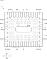
- FIG. 1 is a perspective view showing a semiconductor device according to a first embodiment of the present disclosure.
- FIG. 2 is a plan view showing the semiconductor device according to the first embodiment of the present disclosure.
- FIG. 3 is a bottom view showing the semiconductor device according to the first embodiment of the present disclosure.
- FIG. 4 is a front view showing the semiconductor device according to the first embodiment of the present disclosure.
- FIG. 5 is a right side view showing the semiconductor device according to the first embodiment of the present disclosure.
- FIG. 6 is a cross-sectional view taken along line VI-VI in FIG.
- FIG. 7 is a cross-sectional view taken along line VII-VII in FIG.
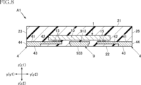
- FIG. 8 is a cross-sectional view taken along line VIII-VIII in FIG.
- FIG. 6 is a cross-sectional view taken along line VI-VI in FIG.
- FIG. 7 is a cross-sectional view taken along line VII-VII in FIG.
- FIG. 8 is a cross-sectional view taken along line VIII-VIII
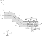
- FIG. 9 is a partial enlarged plan view showing the semiconductor device according to the first embodiment of the present disclosure.
- FIG. 10 is a partially enlarged cross-sectional view taken along line XX in FIG.
- FIG. 11 is a partial enlarged plan view showing the semiconductor device according to the first embodiment of the present disclosure.
- FIG. 12 is a partially enlarged cross-sectional view taken along line XII-XII in FIG.
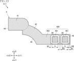
- FIG. 13 is a partial enlarged plan view showing a first modified example of the semiconductor device according to the first embodiment of the present disclosure.
- FIG. 14 is a partial enlarged plan view showing a second modified example of the semiconductor device according to the first embodiment of the present disclosure.
- FIG. 15 is a partial enlarged plan view showing a third modified example of the semiconductor device according to the first embodiment of the present disclosure.
- FIG. 16 is a partial enlarged cross-sectional view showing a fourth modification of the semiconductor device according to the first embodiment of the present disclosure.
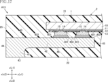
- FIG. 17 is a partial enlarged cross-sectional view showing a fifth modification of the semiconductor device according to the first embodiment of the present disclosure.
- FIG. 18 is a partially enlarged cross-sectional view showing a semiconductor device according to a second embodiment of the present disclosure.
- FIG. 19 is a partially enlarged cross-sectional view showing a semiconductor device according to a third embodiment of the present disclosure.
- an object A is formed on an object B" and “an object A is formed on an object B” include “an object A is formed directly on an object B” and “an object A is formed on an object B with another object interposed between the object A and the object B” unless otherwise specified.
- an object A is disposed on an object B” and “an object A is disposed on an object B” include “an object A is disposed directly on an object B” and “an object A is disposed on an object B with another object interposed between the object A and the object B" unless otherwise specified.
- an object A is located on an object B includes “an object A is located on an object B in contact with an object B” and “an object A is located on an object B with another object interposed between the object A and the object B” unless otherwise specified.
- an object A overlaps an object B when viewed in a certain direction includes “an object A overlaps the entire object B” and “an object A overlaps a part of an object B.”
- a surface A faces in direction B is not limited to the case where the angle of surface A with respect to direction B is 90°, but also includes the case where surface A is tilted with respect to direction B.
- First embodiment: 1 to 12 show a semiconductor device according to a first embodiment of the present disclosure.
- the semiconductor device A1 of this embodiment includes a semiconductor element 1, a sealing resin 2, and a plurality of leads 4, 8, and 9.
- the semiconductor device A1 is a QFN (Quad Flat No leaded package) type semiconductor device, but the basic configuration of the semiconductor device according to the present disclosure is not limited thereto.
- FIG. 1 is a perspective view showing the semiconductor device A1.
- FIG. 2 is a plan view showing the semiconductor device A1.
- FIG. 3 is a bottom view showing the semiconductor device A1.
- FIG. 4 is a front view showing the semiconductor device A1.
- FIG. 5 is a right side view showing the semiconductor device A1.
- FIG. 6 is a cross-sectional view taken along line VI-VI in FIG. 2.
- FIG. 7 is a cross-sectional view taken along line VII-VII in FIG. 2.
- FIG. 8 is a cross-sectional view taken along line VIII-VIII in FIG. 2.
- FIG. 9 is a partially enlarged plan view showing the semiconductor device A1.
- FIG. 10 is a partially enlarged cross-sectional view taken along line X-X in FIG. 9.
- FIG. 11 is a partially enlarged plan view showing the semiconductor device A1.
- FIG. 12 is a partially enlarged cross-sectional view taken along line XII-XII in FIG. 11.
- the thickness direction of the semiconductor element 1 is referred to as the thickness direction z.
- plane view is synonymous with "viewed in the thickness direction z.”
- a direction perpendicular to the thickness direction z is referred to as the first direction x.
- a direction perpendicular to the thickness direction z and the first direction x is referred to as the second direction y.
- the semiconductor element 1 performs the main electrical function of the semiconductor device A1 when the semiconductor device A1 is mounted on a circuit board or the like to form part of an electrical circuit.
- the specific configuration of the semiconductor element 1 is not limited in any way, and includes an LSI (Large Scale Integration), an IC (Integrated Circuit), and the like.
- the semiconductor element 1 of this embodiment is rectangular in shape with two sides along the first direction x and two sides along the second direction y when viewed in the z direction.
- the semiconductor element 1 has an element body 10 and a number of electrodes 15.
- the element body 10 is a main body portion that includes a semiconductor material such as Si (silicon), and includes, for example, a functional circuit (not shown).
- the multiple electrodes 15 are for flip-chip mounting the semiconductor element 1 to the multiple leads 4, 9.
- the electrodes 15 are an example of a joining object of the present disclosure.
- the multiple electrodes 15 protrude from the element body 10 toward the z2 side in the thickness direction z.
- the material of the electrodes 15 is not limited in any way and includes metals such as Cu (copper) and Cu (copper) alloys.
- a plating layer (not shown) containing, for example, Ni (nickel) may be appropriately provided on the tip of the electrode 15 on the z2 side in the thickness direction z.
- the semiconductor element 1 has a wiring layer 11, a first protective layer 12, a second protective layer 13, and an underlayer 14.
- the wiring layer 11 is disposed on the z2 side of the element body 10 in the thickness direction z.
- the wiring layer 11 is electrically connected to a functional circuit (not shown) formed in the element body 10.
- the wiring layer 11 includes, for example, Al (aluminum).
- the first protective layer 12 covers the wiring layer 11 from the z2 side of the thickness direction z.
- the first protective layer 12 includes, for example, SiN (silicon nitride).
- the first protective layer 12 has an opening that exposes a part of the wiring layer 11.
- the second protective layer 13 covers the first protective layer 12 from the z2 side of the thickness direction z.
- the second protective layer 13 includes, for example, polyimide.
- the second protective layer 13 has an opening that overlaps with the opening of the first protective layer 12.
- the underlayer 14 is provided so as to cover the opening of the second protective layer 13.
- the second protective layer 13 contains, for example, Cu (copper), Ni (nickel), etc.
- the electrode 15 is formed by growing a metal on the second protective layer 13, for example, by plating.
- the sealing resin 2 covers the semiconductor element 1 and a portion of each of the leads 4, 8, and 9.
- the specific configuration of the sealing resin 2 is not limited, and the constituent material thereof includes, for example, epoxy resin.
- the sealing resin 2 of this embodiment has a resin main surface 21, a resin back surface 22, a first resin side surface 23, a second resin side surface 24, a third resin side surface 25, and a fourth resin side surface 26.
- the resin main surface 21 faces the z1 side in the z direction, and in the illustrated example, is a flat rectangular surface.
- the resin back surface 22 faces the z2 side in the z direction, and in the illustrated example, is a flat rectangular surface.
- the first resin side surface 23 is a surface along the first direction x and z directions, and faces the y1 side in the second direction y.
- the second resin side surface 24 is a surface along the second direction y and z directions, and faces the x1 side in the first direction x.
- the third resin side surface 25 is a surface along the second direction y and z directions, and faces the x2 side in the first direction x.
- the fourth resin side surface 26 is a surface along the first direction x and z directions, and faces the y2 side in the second direction y.
- the length in the first direction x of the first resin side surface 23 and the fourth resin side surface 26 is longer than the length in the second direction y of the second resin side surface 24 and the third resin side surface 25.
- the multiple leads 4, 8, 9 perform functions such as supporting the semiconductor element 1 and forming a conductive path to the semiconductor element 1.
- the specific configuration of the multiple leads 4, 8, 9 is not limited in any way.
- the multiple leads 4, 8, 9 include, as constituent materials, for example, Cu (copper), Ni (nickel), Fe (iron), and alloys thereof. In the following explanation, the multiple leads 4, 8, 9 will be distinguished and explained as multiple leads 4, multiple corner leads 8, and center lead 9.
- the multiple leads 4 are arranged in the first direction x and the second direction y, and are arranged in a rectangular shape.
- the lead 4 has a lead body 40 and a metal layer 49.
- Figs. 9 and 10 show the second lead 4 counting from the y2 side of the second direction y among the multiple leads 4 arranged on the x2 side of the first direction x in Fig. 2.
- Figs. 11 and 12 show the first lead 4 counting from the y2 side of the second direction y among the multiple leads 4 arranged on the x2 side of the first direction x in Fig. 2.
- the semiconductor element 1 and the sealing resin 2 are omitted for ease of understanding.
- the lead body 40 is the main body portion that constitutes the majority of the lead 4, and contains the above-mentioned Cu (copper), Ni (nickel), Fe (iron), and alloys thereof.
- the lead body 40 has a main surface 400, a thick portion 41, a thin portion 42, a mounting surface 43, an end surface 44, a side surface 45, and an intermediate surface 46.
- the thick portion 41 is a portion of the lead 4 that is relatively thicker in the thickness direction z (compared to the thin portion 42).
- the thin portion 42 is a portion of the lead 4 that is relatively thinner in the thickness direction z (compared to the thick portion 41).
- the shapes of the thick portion 41 and the thin portion 42 as viewed in the thickness direction z are appropriately set depending on, for example, the position where the semiconductor element 1 is mounted, etc.
- the principal surface 400 faces the z1 side in the thickness direction z.
- the principal surface 400 faces the electrode 15 of the semiconductor element 1.
- the principal surface 400 is formed across both the thick portion 41 and the thin portion 42.
- the principal surface 400 is covered with the sealing resin 2.
- the mounting surface 43 is the surface exposed from the resin back surface 22 of the sealing resin 2, and is formed in the thick portion 41. In the illustrated example, the mounting surface 43 is flush with the resin back surface 22.
- the end face 44 is a surface exposed from the first resin side face 23, the second resin side face 24, the third resin side face 25, and the fourth resin side face 26 of the sealing resin 2, and faces the first direction x or the second direction y.
- the end face 44 is formed in the thick portion 41.
- the mounting surface 43 and the end face 44 are connected.
- a concave surface or the like may be interposed between the mounting surface 43 and the end face 44.
- the mounting surface 43 and the end face 44 may be appropriately provided with a plating layer (not illustrated) containing, for example, Sn (tin) or the like.
- the end face 44 is flush with any of the first resin side face 23, the second resin side face 24, the third resin side face 25, and the fourth resin side face 26.
- the side surface 45 faces in a direction intersecting the thickness direction z, and is located between the main surface 400 and the end surface 443 in the thickness direction z.
- the side surface 45 is covered with the sealing resin 2.
- the intermediate surface 46 is formed in the thin-walled portion 42.
- the intermediate surface 46 is located between the main surface 400 and the mounting surface 43 in the thickness direction z, and faces the z2 side in the thickness direction z, like the mounting surface 43.
- the intermediate surface 46 is covered with the sealing resin 2.
- the intermediate surface 46 is separated from the resin back surface 22 on the z1 side in the thickness direction z.
- the metal layer 49 is disposed on the main surface 400.
- the metal layer 49 is a member to which the conductive bonding material 19 is bonded.
- the material of the metal layer 49 has better wettability with the conductive bonding material 19 in a molten state than the material of the lead body 40.
- the shape of the metal layer 49 is not limited in any way, and various shapes such as a circle, an ellipse, a polygon, etc. can be adopted. In the illustrated example, the metal layer 49 is a circle.
- the main surface 400 includes a smooth region 401 and an uneven region 402.
- the uneven region 402 has a rougher surface than the smooth region 401.
- the surface roughness of the uneven region 402 is not limited in any way.
- An example of the surface roughness of the uneven region 402 is an arithmetic mean roughness Ra of 1 ⁇ m or more and 10 ⁇ m or less.
- the method of forming the uneven region 402 is not limited in any way. Examples of the method of forming the uneven region 402 include a roughening process by etching, and a roughening process in which CuO or Cu 2 O (copper oxide) grows in a needle shape. Both the smooth region 401 and the uneven region 402 are covered with the sealing resin 2, and the sealing resin 2 is in direct contact with them.
- the side surface 45 and the intermediate surface 46 are made to have an uneven surface similar to that of the uneven region 402.
- the method of making the end surface 445 and the intermediate surface 46 into an uneven surface may be the same as the method of forming the uneven region 402.
- the uneven region 402 is separated from the metal layer 49 in a planar view.
- the smooth region 401 is located between the metal layer 49 and the uneven region 402 in a planar view.
- the smooth region 401 surrounds the entire periphery of the metal layer 49 in a planar view
- the uneven region 402 surrounds the entire periphery of the smooth region 401.
- the uneven region 402 reaches the edge of the main surface 400 in a plan view. In the illustrated example, the uneven region 402 reaches all edges of the main surface 400. The uneven region 402 may reach only a portion of the edge of the main surface 400, or may not reach the edge of the main surface 400.
- the smooth region 401 is away from the edge of the main surface 400. The smooth region 401 may reach the edge of the main surface 400.
- the size D of the metal layer 49 (in the illustrated example, the diameter of the metal layer 49) is, for example, 50 ⁇ m or more and 200 ⁇ m or less, for example, about 100 ⁇ m.
- the size W1 is the distance between the metal layer 49 and the uneven region 402, and corresponds to the width of the smooth region 401.
- the size W1 may be, for example, 5% or more and 50% or less of the size D.
- the size W2 is the distance between the smooth region 401 and the edge of the main surface 400. In the illustrated example, the size W2 is the distance between the smooth region 401 and the tip portion of the main surface 400 in the first direction x.
- the size W2 may be, for example, 5% or more and 50% or less of the size D.
- the two metal layers 49 are disposed on the main surface 400 of the lead 4.
- the two metal layers 49 are separated from each other.
- the main surface 400 includes two smooth regions 401.
- the two smooth regions 401 surround the two metal layers 49 individually.
- the uneven region 402 has a portion located between the two metal layers 49 (the two smooth regions 401).
- the size W3 is the distance between the two adjacent smooth regions 401.
- the size W3 may be, for example, 5% or more and 90% or less of the size D.
- the size W4 is the distance between the adjacent metal layers 49. In the illustrated example, the size W4 is smaller than the size D.
- Corner lead 8 As shown in FIGS. 1 to 5, the corner leads 8 are arranged at the four corners of the sealing resin 2 when viewed in the thickness direction z.
- the corner lead 8 has a corner mounting surface 83, a first corner end surface 841, and a second corner end surface 842.
- the corner mounting surface 83 faces the z2 side in the thickness direction z and is exposed from the resin back surface 22 of the sealing resin 2.
- the first corner end face 841 faces in the second direction y and is exposed from the first resin side face 23 or the fourth resin side face 26. In the illustrated example, the first corner end face 841 is flush with the first resin side face 23 or the fourth resin side face 26.
- the second corner end face 842 faces in the first direction x and is exposed from the second resin side face 24 or the third resin side face 25. In the illustrated example, the second corner end face 842 is flush with the second resin side face 24 or the third resin side face 25. In the illustrated example, the first corner end face 841 and the second corner end face 842 are connected to each other.
- Center lead 9 1 to 3, 5, and 7, the center lead 9 is disposed between the multiple leads 4 in the second direction y.
- the center lead 9 overlaps with the center of the semiconductor device A1 (sealing resin 2) in the second direction y.
- the center lead 9 has a center thick portion 911, a center thick portion 912, a center thick portion 913, a center thin portion 921, a center thin portion 922, a center mounting surface 931, a center mounting surface 932, a center mounting surface 933, a center end surface 941, and a center end surface 942.
- the center mounting surface 931, center mounting surface 932, and center mounting surface 933 are portions of the center lead 9 that are relatively thick in the thickness direction z (compared to the center thin portion 921 and center thin portion 922).
- the center thick portion 911 has a center mounting surface 931 and a center end surface 941
- the center thick portion 912 has a center mounting surface 932 and a center end surface 942
- the center thick portion 913 has a center mounting surface 933.
- the center thick portion 911 is disposed on the x1 side of the first direction x
- the center thick portion 912 is disposed on the x2 side of the first direction x
- the center thick portion 913 is disposed in the center of the first direction x.
- the center thin portion 921 and the center thin portion 922 are portions of the center lead 9 that are relatively thin in the thickness direction z (compared to the center thick portion 911, the center thick portion 912, and the center thick portion 913), and are spaced apart from the resin back surface 22 on the z1 side in the thickness direction z.
- the semiconductor element 1 is mounted on the center thin portion 921 and the center thin portion 922.
- some of the multiple electrodes 15 of the semiconductor element 1 are conductively joined to the center lead 9.
- the conductive joint between the electrode 15 and the center lead 9 may have the same configuration as the conductive joint between the electrode 15 and the lead 4, for example.
- the center lead 9 may have a configuration including a lead body 40 and a member equivalent to the metal layer 49, similar to the lead 4.
- the center lead 9 may have a surface having a configuration similar to the main surface 400 including a smooth region 401 and an uneven region 402, similar to the lead 4.
- the main surface 400 includes a smooth region 401 and an uneven region 402.
- the smooth region 401 surrounds the metal layer 49.
- the material of the metal layer 49 has better wettability with the conductive bonding material 19 in a molten state than the material of the lead body 40.
- the smooth region 401 is smoother than the uneven region 402, and has worse wettability with the conductive bonding material 19 in a molten state than the uneven region 402. Therefore, when manufacturing the semiconductor device A1, the conductive bonding material 19 in a molten state spreads quickly along the metal layer 49 and is less likely to spread in the smooth region 401.
- the conductive bonding material 19 in a molten state tends to remain on the metal layer 49, and it is possible to suppress the spreading of the conductive bonding material 19 in a molten state in the smooth region 401.
- the uneven region 402 has an uneven shape, and therefore has a higher adhesion strength with the sealing resin 2 than the smooth region 401. Therefore, it is possible to increase the adhesion strength between the lead 4 and the sealing resin 2. Therefore, it is possible to suppress peeling of the sealing resin 2 while maintaining an appropriate bonding state.
- the size W1 is 5% or more and 50% or less of the size D, it helps to prevent unintended spreading of the molten conductive bonding material 19 and peeling of the sealing resin 2.
- the uneven region 402 reaches the edge of the main surface 400. This makes it possible to prevent the sealing resin 2 from peeling off from the main surface 400 at the edge of the main surface 400.
- the uneven region 402 reaches all of the edges of the main surface 400. This helps to prevent the sealing resin 2 from peeling off.
- the side surface 45 is an uneven surface. This results in an uneven surface that spans the uneven region 402 and the side surface 45. This makes it possible to more effectively prevent peeling of the sealing resin 2 at the edge of the main surface 400. As the intermediate surface 46 is an uneven surface, peeling of the sealing resin 2 can be more reliably prevented.
- FIGS. 13 to 19 show modified examples and other embodiments of the present disclosure.
- elements that are the same as or similar to those in the above-described embodiment are given the same reference numerals as in the above-described embodiment.
- the configurations of the various parts in each modified example and each embodiment can be combined with each other as appropriate to the extent that no technical contradictions arise.
- First Modification of First Embodiment shows a first modification of the semiconductor device A1.
- the semiconductor device A11 of this modification is different from the above-described example in the shapes of the electrode 15, the metal layer 49, and the smooth region 401, etc.
- the metal layer 49 is rectangular in plan view.
- the shape of the metal layer 49 corresponds to the shape of the electrode 15, which is rectangular, for example.
- the smooth region 401 is rectangular and annular in plan view.
- the size D is, for example, the length of one side of the metal layer 49, or the size in the first direction x in which two metal layers 49 are adjacent to each other.
- This modified example also makes it possible to suppress peeling of the sealing resin 2 while maintaining an appropriate bonded state.
- the shapes of the electrode 15, metal layer 49, and smooth region 401 are not limited in any way.
- Second Modification of First Embodiment 14 shows a second modification of the semiconductor device A12.
- the semiconductor device A12 of this modification has a different shape of the smooth region 401 and the uneven region 402 from the above-mentioned example.
- one smooth region 401 surrounds two metal layers 49. That is, the uneven region 402 does not exist between adjacent metal layers 49.
- the size W4 may be smaller than the size W4 in the semiconductor device A1, and may be, for example, less than half the size D.
- This modified example also makes it possible to suppress peeling of the sealing resin 2 while maintaining an appropriate bonding state.
- Third Modification of First Embodiment shows a third modification of the semiconductor device A13.
- the semiconductor device A13 of this modification has a different shape of the smooth region 401 and the uneven region 402 from the above-described examples.
- the smooth region 401 reaches the edge of the main surface 400 in a plan view.
- a portion of the edge of the main surface 400 is not in contact with the uneven region 402.
- the edge of the main surface 400 on the x1 side in the first direction x (the edge opposite the end surface 44) is in contact with the uneven region 402.
- This modified example also makes it possible to suppress peeling of the sealing resin 2 while maintaining an appropriate bonding state.
- the edge on the x1 side in the first direction x of the main surface 400 (the edge opposite the end surface 44) is in contact with the uneven region 402, thereby making it possible to suppress peeling between the end of the main surface 400 on the x1 side in the first direction x and the sealing resin 2.
- Fourth Modification of First Embodiment 16 shows a fourth modification of the semiconductor device A1.
- the semiconductor device A14 of this modification has a different configuration of the leads 4 from the above-mentioned examples.
- the intermediate surface 46 is a smooth surface compared to the uneven area 402 and the side surface 45. This modified example also makes it possible to suppress peeling of the sealing resin 2 while maintaining an appropriate bonding state. As can be understood from this modified example, the intermediate surface 46 may be a smooth surface.
- the side surface 45 is a smooth surface compared to the uneven area 402. This modified example also makes it possible to suppress peeling of the sealing resin 2 while maintaining an appropriate bonding state. As can be understood from this modified example, the side surface 45 may be a smooth surface.
- Second embodiment: 18 shows a semiconductor device according to a second embodiment of the present disclosure.
- the semiconductor device A2 of this embodiment includes a conductive member 5.
- the conductive member 5 is electrically connected to, for example, the semiconductor element 1 (not shown).
- the conductive member 5 includes, for example, Cu (copper), Ni (nickel), Fe (iron), and alloys thereof.
- the conductive member 5 is electrically connected to the metal layer 49 of the lead 4 via a conductive bonding material 59.
- the conductive member 5 is an example of an object to be bonded in this disclosure.
- the conductive bonding material 59 has a configuration similar to that of the conductive bonding material 19 described above.
- This embodiment also makes it possible to suppress peeling of the sealing resin 2 while maintaining an appropriate bonding state.
- the objects to be bonded in this disclosure are not limited in any way and may be members that contain metal, such as the conductive member 5.
- Third embodiment: 19 shows a semiconductor device according to a third embodiment of the present disclosure.
- a semiconductor element 1 corresponds to the object to be joined of the present disclosure.
- the semiconductor element 1 of this embodiment has a metal layer 18.
- the metal layer 18 is disposed on the z2 side of the element body 10 in the thickness direction z.
- the metal layer 18 contains, for example, Cu (copper), Al (aluminum), Ni (nickel), etc.
- the metal layer 18 and the metal layer 49 are joined by a conductive bonding material 19.
- the conductive bonding material 19 is not limited in any way and is, for example, Ag (silver) paste.
- the object to be bonded in this disclosure is not limited in any way and may be the semiconductor element 1 (metal layer 18).
- the conductive bonding material 19 may be of various configurations, such as solder or Ag (silver) paste.
- the semiconductor device according to the present disclosure is not limited to the above-mentioned embodiment.
- the specific configuration of each part of the semiconductor device according to the present disclosure can be freely designed in various ways.
- the present disclosure includes the embodiments described in the following appendix.
- Appendix 1 A semiconductor element; Lead and An object to be joined; A conductive bonding material that electrically connects the object to be bonded and the lead; a sealing resin that covers the object to be joined and at least a part of the lead,
- the lead includes a lead body having a main surface facing the bonding object, and a metal layer disposed on the main surface, The material of the metal layer has a higher wettability with respect to the conductive bonding material in a molten state than the material of the lead body, the conductive bonding material is bonded to the metal layer,
- the main surface includes, in a plan view, a rough region separated from the metal layer, and a smooth region located between the metal layer and the rough region. Appendix 2. 2.
- Appendix 3. The semiconductor device according to claim 1, wherein a minimum distance between the metal layer and the uneven region in a planar view is 5% or more and 50% or less of a size of the metal layer.
- Appendix 4. 4. The semiconductor device according to claim 2, wherein the uneven region reaches an edge of the main surface in a plan view.
- Appendix 5. the lead body has a side surface facing a direction intersecting the main surface and covered with the sealing resin, The semiconductor device according to claim 4, wherein the side surface is an uneven surface.
- the lead body has a mounting surface facing the opposite side to the main surface and exposed from the sealing resin, and an intermediate surface located between the main surface and the mounting surface and facing the same side as the mounting surface; 6.
- Appendix 7. The semiconductor device according to claim 2, wherein the lead has two of the metal layers adjacent to each other.
- the uneven region includes a portion located between two of the metal layers.
- Appendix 9. 9.
- the semiconductor device according to claim 8, wherein the distance between the two metal layers in a planar view is smaller than the size of the metal layers in a planar view.
- Appendix 10. 8 The semiconductor device of claim 7, wherein the uneven region is not present between two of the metal layers. Appendix 11.
Landscapes
- Structures Or Materials For Encapsulating Or Coating Semiconductor Devices Or Solid State Devices (AREA)
- Engineering & Computer Science (AREA)
- Microelectronics & Electronic Packaging (AREA)
Priority Applications (2)
| Application Number | Priority Date | Filing Date | Title |
|---|---|---|---|
| JP2024572941A JPWO2024157758A1 (https=) | 2023-01-25 | 2024-01-10 | |
| US19/273,673 US20250343168A1 (en) | 2023-01-25 | 2025-07-18 | Semiconductor device |
Applications Claiming Priority (2)
| Application Number | Priority Date | Filing Date | Title |
|---|---|---|---|
| JP2023009199 | 2023-01-25 | ||
| JP2023-009199 | 2023-01-25 |
Related Child Applications (1)
| Application Number | Title | Priority Date | Filing Date |
|---|---|---|---|
| US19/273,673 Continuation US20250343168A1 (en) | 2023-01-25 | 2025-07-18 | Semiconductor device |
Publications (1)
| Publication Number | Publication Date |
|---|---|
| WO2024157758A1 true WO2024157758A1 (ja) | 2024-08-02 |
Family
ID=91970328
Family Applications (1)
| Application Number | Title | Priority Date | Filing Date |
|---|---|---|---|
| PCT/JP2024/000256 Ceased WO2024157758A1 (ja) | 2023-01-25 | 2024-01-10 | 半導体装置 |
Country Status (3)
| Country | Link |
|---|---|
| US (1) | US20250343168A1 (https=) |
| JP (1) | JPWO2024157758A1 (https=) |
| WO (1) | WO2024157758A1 (https=) |
Citations (10)
| Publication number | Priority date | Publication date | Assignee | Title |
|---|---|---|---|---|
| JP2006310397A (ja) * | 2005-04-26 | 2006-11-09 | Dainippon Printing Co Ltd | 回路部材、回路部材の製造方法、半導体装置、及び回路部材表面の積層構造 |
| JP2014007363A (ja) * | 2012-06-27 | 2014-01-16 | Renesas Electronics Corp | 半導体装置の製造方法および半導体装置 |
| JP2016105432A (ja) * | 2014-12-01 | 2016-06-09 | Shマテリアル株式会社 | リードフレームの製造方法 |
| JP2019016705A (ja) * | 2017-07-07 | 2019-01-31 | 新光電気工業株式会社 | 電子部品装置及びその製造方法 |
| JP2019096694A (ja) * | 2017-11-21 | 2019-06-20 | 新光電気工業株式会社 | リードフレーム、半導体装置、リードフレームの製造方法 |
| JP2019186326A (ja) * | 2018-04-05 | 2019-10-24 | ルネサスエレクトロニクス株式会社 | 半導体装置およびその製造方法 |
| JP2020077747A (ja) * | 2018-11-07 | 2020-05-21 | 新光電気工業株式会社 | リードフレーム、半導体装置及びリードフレームの製造方法 |
| WO2021193338A1 (ja) * | 2020-03-26 | 2021-09-30 | ローム株式会社 | 半導体装置 |
| JP2022103594A (ja) * | 2020-12-28 | 2022-07-08 | 新光電気工業株式会社 | リードフレーム、リードフレームの製造方法及び半導体装置 |
| JP2022143169A (ja) * | 2021-03-17 | 2022-10-03 | ローム株式会社 | 半導体装置 |
-
2024
- 2024-01-10 WO PCT/JP2024/000256 patent/WO2024157758A1/ja not_active Ceased
- 2024-01-10 JP JP2024572941A patent/JPWO2024157758A1/ja active Pending
-
2025
- 2025-07-18 US US19/273,673 patent/US20250343168A1/en active Pending
Patent Citations (10)
| Publication number | Priority date | Publication date | Assignee | Title |
|---|---|---|---|---|
| JP2006310397A (ja) * | 2005-04-26 | 2006-11-09 | Dainippon Printing Co Ltd | 回路部材、回路部材の製造方法、半導体装置、及び回路部材表面の積層構造 |
| JP2014007363A (ja) * | 2012-06-27 | 2014-01-16 | Renesas Electronics Corp | 半導体装置の製造方法および半導体装置 |
| JP2016105432A (ja) * | 2014-12-01 | 2016-06-09 | Shマテリアル株式会社 | リードフレームの製造方法 |
| JP2019016705A (ja) * | 2017-07-07 | 2019-01-31 | 新光電気工業株式会社 | 電子部品装置及びその製造方法 |
| JP2019096694A (ja) * | 2017-11-21 | 2019-06-20 | 新光電気工業株式会社 | リードフレーム、半導体装置、リードフレームの製造方法 |
| JP2019186326A (ja) * | 2018-04-05 | 2019-10-24 | ルネサスエレクトロニクス株式会社 | 半導体装置およびその製造方法 |
| JP2020077747A (ja) * | 2018-11-07 | 2020-05-21 | 新光電気工業株式会社 | リードフレーム、半導体装置及びリードフレームの製造方法 |
| WO2021193338A1 (ja) * | 2020-03-26 | 2021-09-30 | ローム株式会社 | 半導体装置 |
| JP2022103594A (ja) * | 2020-12-28 | 2022-07-08 | 新光電気工業株式会社 | リードフレーム、リードフレームの製造方法及び半導体装置 |
| JP2022143169A (ja) * | 2021-03-17 | 2022-10-03 | ローム株式会社 | 半導体装置 |
Also Published As
| Publication number | Publication date |
|---|---|
| JPWO2024157758A1 (https=) | 2024-08-02 |
| US20250343168A1 (en) | 2025-11-06 |
Similar Documents
| Publication | Publication Date | Title |
|---|---|---|
| US11362012B2 (en) | Semiconductor device | |
| US20230352375A1 (en) | Semiconductor device | |
| US6677674B2 (en) | Semiconductor package having two chips internally connected together with bump electrodes and both chips externally connected to a lead frame with bond wires | |
| KR100470386B1 (ko) | 멀티-칩패키지 | |
| JP4633971B2 (ja) | 半導体装置 | |
| US5773888A (en) | Semiconductor device having a bump electrode connected to an inner lead | |
| JPH09237962A (ja) | 電子回路装置 | |
| JPH10308466A (ja) | ヒートシンク付着ボールグリッドアレイ半導体パッケージ | |
| JPH10200012A (ja) | ボールグリッドアレイ半導体のパッケージ及び製造方法 | |
| US20050054187A1 (en) | Method for forming ball pads of BGA substrate | |
| JP7037368B2 (ja) | 半導体装置および半導体装置の製造方法 | |
| US20050017375A1 (en) | Ball grid array package substrate and method for manufacturing the same | |
| EP4053886A1 (en) | Method for fabricating a substrate with a solder stop structure, substrate with a solder stop structure and electronic device | |
| US7030492B2 (en) | Under bump metallurgic layer | |
| WO2024157758A1 (ja) | 半導体装置 | |
| JP7550932B2 (ja) | 半導体装置 | |
| JPH09162240A (ja) | 半導体装置 | |
| WO2025033276A1 (ja) | 半導体装置 | |
| US20250372486A1 (en) | Semiconductor device | |
| US20250022822A1 (en) | Semiconductor element and semiconductor device | |
| JP2702455B2 (ja) | ピングリッドアレイ型半導体装置 | |
| US20250293124A1 (en) | Semiconductor device and method for manufacturing the same | |
| JP7675786B1 (ja) | 半導体装置 | |
| JP3169072B2 (ja) | 半導体装置 | |
| JP2025121431A (ja) | 半導体装置 |
Legal Events
| Date | Code | Title | Description |
|---|---|---|---|
| 121 | Ep: the epo has been informed by wipo that ep was designated in this application |
Ref document number: 24747089 Country of ref document: EP Kind code of ref document: A1 |
|
| ENP | Entry into the national phase |
Ref document number: 2024572941 Country of ref document: JP Kind code of ref document: A |
|
| WWE | Wipo information: entry into national phase |
Ref document number: 2024572941 Country of ref document: JP |
|
| NENP | Non-entry into the national phase |
Ref country code: DE |
|
| 122 | Ep: pct application non-entry in european phase |
Ref document number: 24747089 Country of ref document: EP Kind code of ref document: A1 |