WO2024157567A1 - 電流センサ - Google Patents
電流センサ Download PDFInfo
- Publication number
- WO2024157567A1 WO2024157567A1 PCT/JP2023/040148 JP2023040148W WO2024157567A1 WO 2024157567 A1 WO2024157567 A1 WO 2024157567A1 JP 2023040148 W JP2023040148 W JP 2023040148W WO 2024157567 A1 WO2024157567 A1 WO 2024157567A1
- Authority
- WO
- WIPO (PCT)
- Prior art keywords
- current sensor
- bus bar
- metal
- metallic material
- magnetic detection
- Prior art date
- Legal status (The legal status is an assumption and is not a legal conclusion. Google has not performed a legal analysis and makes no representation as to the accuracy of the status listed.)
- Ceased
Links
Images






Classifications
-
- G—PHYSICS
- G01—MEASURING; TESTING
- G01R—MEASURING ELECTRIC VARIABLES; MEASURING MAGNETIC VARIABLES
- G01R15/00—Details of measuring arrangements of the types provided for in groups G01R17/00 - G01R29/00, G01R33/00 - G01R33/26 or G01R35/00
- G01R15/14—Adaptations providing voltage or current isolation, e.g. for high-voltage or high-current networks
- G01R15/20—Adaptations providing voltage or current isolation, e.g. for high-voltage or high-current networks using galvano-magnetic devices, e.g. Hall-effect devices, i.e. measuring a magnetic field via the interaction between a current and a magnetic field, e.g. magneto resistive or Hall effect devices
- G01R15/207—Constructional details independent of the type of device used
-
- G—PHYSICS
- G01—MEASURING; TESTING
- G01R—MEASURING ELECTRIC VARIABLES; MEASURING MAGNETIC VARIABLES
- G01R15/00—Details of measuring arrangements of the types provided for in groups G01R17/00 - G01R29/00, G01R33/00 - G01R33/26 or G01R35/00
- G01R15/14—Adaptations providing voltage or current isolation, e.g. for high-voltage or high-current networks
- G01R15/20—Adaptations providing voltage or current isolation, e.g. for high-voltage or high-current networks using galvano-magnetic devices, e.g. Hall-effect devices, i.e. measuring a magnetic field via the interaction between a current and a magnetic field, e.g. magneto resistive or Hall effect devices
-
- G—PHYSICS
- G01—MEASURING; TESTING
- G01R—MEASURING ELECTRIC VARIABLES; MEASURING MAGNETIC VARIABLES
- G01R19/00—Arrangements for measuring currents or voltages or for indicating presence or sign thereof
- G01R19/0092—Measuring current only
Definitions
- the present invention relates to a current sensor that detects a magnetic field generated by a current to be measured flowing through a bus bar and measures the current value of the measured current from the detected magnetic field.
- Patent Document 1 describes a current sensor that is equipped with a bus bar, a shield plate, a magnetic detection element, and a conductive plate, and aims to improve pulse response, and uses a plate-shaped electrical conductor made of copper, aluminum, or the like as the bus bar.
- an object of the present invention is to provide a current sensor equipped with bus bars that are effective in reducing weight and cost.
- a current sensor comprising a bus bar through which a current to be measured flows, and a magnetic detection unit arranged opposite the bus bar and detecting a magnetic field generated in the bus bar, characterized in that the bus bar is made of a laminated material in which a first metal-based material and a second metal-based material which are dissimilar metal-based materials are laminated together, the first metal-based material having a higher density than the second metal-based material and a lower electrical resistivity than the second metal-based material, and the magnetic detection unit is arranged opposite a surface of the bus bar made of the first metal-based material.
- the ratio of metallic materials with different densities and electrical resistivities can be adjusted to achieve a balance between reducing the amount of heat generated by the busbar when the current to be measured flows and making the busbar lighter.
- a dimension of the second metallic material may be larger than a dimension of the first metallic material in a stacking direction.
- a dimension of the second metallic material may be 80% or more of a dimension of the laminated materials in a lamination direction.
- a current sensor comprising a bus bar through which a current to be measured flows, and a magnetic detection unit arranged opposite the bus bar and detecting a magnetic field generated in the bus bar, characterized in that the bus bar is made of a laminated material in which a first metal-based material and a second metal-based material which are dissimilar metal-based materials are laminated together, the first metal-based material having a higher density than the second metal-based material and a lower electrical resistivity than the second metal-based material, and the magnetic detection unit is arranged opposite a surface of the bus bar made of the second metal-based material.
- the laminated structure of two types of metallic materials makes it possible to achieve a balance between reducing the amount of heat generated by the bus bar when the current to be measured flows and making the bus bar lighter.
- a dimension of the second metallic material may be larger than a dimension of the first metallic material in a stacking direction.
- a dimension of the second metallic material may be 60% or more of a dimension of the laminated material in a lamination direction.
- a current sensor having a plurality of measurement phases each consisting of a bus bar through which a current to be measured flows and a magnetic detection unit disposed opposite the bus bar and detecting a magnetic field generated in the bus bar, the bus bar being made of a laminated material in which a first metal-based material and a second metal-based material which are different metal-based materials are laminated, the first metal-based material having a density greater than that of the second metal-based material and a lower electrical resistivity than that of the second metal-based material, a first measurement phase in which the magnetic detection unit is disposed so as to face the surface of the bus bar made of the first metal-based material, and a second measurement phase in which the magnetic detection unit is disposed so as to face the surface of the bus bar made of the second metal-based material.
- the first metallic material has a lower electrical resistivity than the second metallic material, a larger amount of the current to be measured flows through the first metallic material. Therefore, by arranging the magnetic detection unit so that it faces the surface made of the first metallic material, the magnetic field density detected by the magnetic detection unit becomes larger, and the detection accuracy of the first measurement phase becomes better than that of the second measurement phase. For this reason, by designating the measurement phase that requires high detection accuracy as the first measurement phase, it is possible to arrange multiple measurement phases according to the required detection accuracy.
- the second measurement phase may be disposed on both sides of the first measurement phase.
- the measurement error of a measurement phase increases due to the influence of the adjacent measurement phases on both sides. Therefore, when adjacent measurement phases are provided, the adjacent measurement phases are set as second measurement phases and the central measurement phase is set as the first measurement phase, thereby suppressing the decrease in detection accuracy of the first measurement phase and reducing the difference in measurement accuracy among the multiple measurement phases.
- a dimension of the second metallic material may be larger than a dimension of the first metallic material in a stacking direction.
- the bus bar may have a bent portion
- the magnetic detection unit may be disposed at a position capable of detecting an induced magnetic field from two portions of the bus bar positioned on either side of the bent portion.
- the bus bar may be provided with a layer of the first metallic material on a side where the bent portion is bent, and the magnetic detection portion may face the layer of the first metallic material of the bus bar.
- the first metallic material may be a copper-based material and the second metallic material may be an aluminum-based material.
- the properties of the busbar can be adjusted, making it possible to provide a current sensor suitable for miniaturization and thinning.
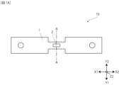
- FIG. 2 is a plan view of the current sensor according to the first embodiment.
- FIG. 1B is a cross-sectional view of the current sensor taken along line AA in FIG. 1A.
- 1C is a graph showing a simulation result of the ratio of an Al thickness T4 to a total thickness T1 and the busbar phase characteristics when the busbar in FIG. 1B is made of Cu and Al.
- FIG. 1C is a cross-sectional view of the current sensor of FIG. 1B with a magnetic shield.
- FIG. 11 is a cross-sectional view of a current sensor according to a second embodiment.
- 5 is a graph showing a simulation result of the ratio of an Al thickness T4 to a total thickness T1 and the busbar phase characteristics when the busbar in FIG. 4 is made of Cu and Al.
- FIG. 5 is a cross-sectional view of the current sensor of FIG. 4 provided with a magnetic shield.
- 1 is a graph showing a difference in magnetic flux density depending on a lamination order and an Al ratio in a bus bar in which Al and Cu are laminated.
- 11 is a graph showing the difference in influence on adjacent bus bars depending on the lamination order and Al ratio in a bus bar in which Al and Cu are laminated.
- FIG. 11 is a cross-sectional view showing a multi-phase type current sensor according to a third embodiment.
- FIG. 13 is a perspective view showing a multi-phase type current sensor according to a modified example.
- FIG. 13 is a perspective view showing a multiphase type current sensor according to another modified example.
- FIG. 11B is a cross-sectional view of the current sensor taken along line BB in FIG. 11A.
- 11B is a graph showing the relationship between the frequency and the phase angle of the current flowing through the bus bar of the reference example of FIG. 11A .
- 11B is a graph showing the relationship between the frequency and gain of a current flowing through the bus bar of the reference example of FIG. 11A.
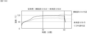
- 13 is a graph showing temperature changes over time when a current to be measured is passed through a conventional bus bar having an Al fastening portion and an Al body portion.
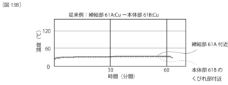
- FIG. 11 is a graph showing temperature changes over time when a current to be measured is passed through a conventional bus bar having a fastening portion made of Cu and a body portion made of Cu.
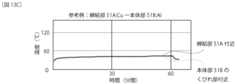
- 13 is a graph showing temperature changes over time when a current to be measured is passed through a reference bus bar having a fastening portion made of Cu and a main body portion made of Al.
- FIG. 13 is a plan view of a current sensor according to another reference example.
- FIG. 14B is a cross-sectional view of the current sensor taken along line BB in FIG. 14A.
- FIG. 1 is a plan view of a conventional current sensor.
- 15B is a cross-sectional view of the current sensor taken along line AA in FIG. 15A.
- FIG. 15B is a cross-sectional view of the current sensor taken along line BB in FIG. 15A.
- the extension direction of the bus bar is the X direction
- the direction perpendicular to the X direction on the opposing surface of the bus bar facing the magnetic detection unit is the Y direction
- the direction perpendicular to the X and Y directions is the Z direction.
- the Y direction is the direction of the sensitivity axis of the magnetic detection unit
- the X and Z directions are perpendicular to the sensitivity axis.
- FIG. 15A is a plan view of a conventional current sensor 60
- FIG. 15B is a cross-sectional view of the current sensor 60 taken along line AA in FIG. 15A.
- a plate-shaped conductor is used as the bus bar 61 through which the current to be measured flows.
- the conductor material include copper and aluminum, and copper, which has good electrical conductivity, is often used alone.
- the bus bar 61 is made of only copper, it may be difficult to meet the increasing and higher level of requirements for the current sensor, such as low cost and weight reduction. Therefore, in the present invention, a bus bar made of a laminated material in which different metal materials are laminated is used in order to realize low cost and weight reduction of the current sensor.
- the current sensor 10 includes a bus bar 1 through which a current to be measured flows, and a magnetic detection unit 2 that is disposed opposite the bus bar 1 and detects a magnetic field generated in the bus bar 1.
- the busbar 1 is made of a laminated material obtained by laminating dissimilar metal-based materials, a first metal-based material 3 and a second metal-based material 4.
- both the first metal-based material 3 and the second metal-based material 4 are configured as layers having a uniform thickness in the Z direction.
- the first metal-based material 3 has a higher density than the second metal-based material 4 (in other words, the first metal-based material 3 is heavier than the second metal-based material 4), and has a lower electrical resistivity (hereinafter referred to as "resistivity" as appropriate) than the second metal-based material 4.
- the magnetic detection portion 2 of the current sensor 10 is disposed opposite to a surface 3S of the busbar 1 that is made of a first metallic material 3 .
- first metal-based material 3 for example, a copper-based material can be used, and as the second metal-based material 4, an aluminum-based material can be used.
- Copper-based materials refer to pure copper, copper alloys, and conductive materials containing these
- aluminum-based materials refer to pure aluminum, aluminum alloys, and conductive materials containing these.
- the bus bar has a high resistivity when made of Al. Therefore, when the current to be measured flows through the bus bar, the temperature of the magnetic detection unit 2 increases due to the heat generated by the bus bar. If the temperature exceeds the heat resistance temperature, the detection accuracy of the current sensor 10 may be degraded.
- Figure 2 is a graph showing the results of a simulation performed on the busbar 1 made of the laminate material shown in Figure 1B, in which Cu is used as the first metallic material 3 and Al is used as the second metallic material 4, while varying the thickness T3 of Cu and the thickness T4 of Al in the Z direction.
- the busbar 1 used in the simulation of Figure 2 has the laminated structure shown in Figure 1B, with a layer of Cu as the first metal-based material 3 arranged on the Z2 side, which is the magnetic detection unit 2 side, and a layer of Al as the second metal-based material 4 arranged on the Z1 side opposite the magnetic detection unit 2.
- the graph in Figure 2 shows that when the phase characteristic on the vertical axis is 0.0°, this is an ideal state in which there is no delay in the output voltage of the current sensor 10 relative to the current being measured, and that the delay in the output voltage increases as you move downward on the vertical axis (towards -1.0°). If this delay is large, the time delay in the output voltage of the current sensor 10 relative to the current being measured in the high frequency band increases, so it is preferable for the phase characteristic on the vertical axis to be closer to 0.0°.
- This graph shows that the delay in the output voltage of the current sensor 10 is smallest when a busbar 1 with an Al ratio of 100% is used, and that there is an inflection point in the phase characteristic at an Al ratio of 60 to 80%.
- FIG. 3 is a cross-sectional view of the current sensor 10 provided with magnetic shields 5A and 5B.
- the current sensor 10 may be provided with magnetic shields 5A and 5B on both sides in the Z direction, sandwiching the bus bar 1 and the magnetic detection unit 2.
- the magnetic shields 5A and 5B can suppress magnetic noise from the outside to the magnetic detection unit 2, improving the measurement accuracy of the current sensor 10.
- the magnetic shield may be provided only on the Z1 side of the bus bar 1 or only on the Z2 side of the magnetic detection unit 2 (a configuration in which only one of the magnetic shields 5A and 5B is provided).
- the magnetic shields 5A and 5B are, for example, made up of multiple metal plate-like bodies of the same shape stacked on top of each other. Note that in the figures used for the explanation, the magnetic shields 5A and 5B are illustrated as a single plate-like body to simplify the multiple plate-like bodies stacked on top of each other.
- a U-shaped magnetic shield having a U-shaped cross section taken along line AA in FIG. 1A may be used. More specifically, the busbar 1 may be shaped into a U-shape on both sides of the busbar 1 in the Y direction and on the Z1 direction side, and a U-shaped magnetic shield may be used that surrounds the magnetic detection unit 2.
- FIG. 4 is a cross-sectional view of the current sensor 11 according to the present embodiment.
- Current sensor 11 of the present embodiment is the same as current sensor 10 in that the laminate material constituting busbar 1 is formed by laminating first metal-based material 3 and second metal-based material 4.
- current sensor 11 differs from current sensor 10 in that magnetic detection unit 2 is disposed facing surface 4S of busbar 1 made of second metal-based material 4, in that magnetic detection unit 2 is disposed facing surface 3S of busbar 1 made of first metal-based material 3.
- Figure 5 is a graph showing the results of a simulation in which the thickness T3 of Cu and the thickness T4 of Al in the Z direction are changed when a laminate material in which the first metal material 3 is Cu and the second metal material 4 is Al is used as the busbar 1 shown in Figure 4.
- the horizontal axis in the figure shows the ratio of the thickness T4 of Al to the thickness T1 of the busbar 1.
- the busbar 1 for which the simulation results are shown in Figure 5, has the laminated structure shown in Figure 4, with a layer of Al as the second metal-based material 4 disposed on the magnetic detection section 2 side, and a layer of Cu as the first metal-based material 3 disposed on the opposite side of the magnetic detection section 2, sandwiching the layer of the second metal-based material 4.
- the vertical and horizontal axes in the graph of Figure 5 show the same contents as those in the graph of Figure 2.
- This graph shows that the delay in the output voltage of the current sensor 10 is smallest when a busbar 1 with an Al ratio of 100% is provided, and that there is an inflection point in the phase characteristics when the Al ratio is between 40% and 60%.
- the thickness T4 which is the dimension of the second metallic material 4 in the Z direction, which is the lamination direction, is greater than the thickness T3, which is the dimension of the first metallic material 3. Furthermore, when the thickness T1, which is the dimension of the busbar 1 made of the laminated material, in the lamination direction, is taken as 100%, it is even more preferable that the thickness T4 of the second metallic material 4 is 60% or more.
- FIG. 6 is a cross-sectional view of a current sensor 11 provided with magnetic shields 5A and 5B.
- the current sensor 11 may be provided with magnetic shields 5A and 5B on both sides in the Z direction, sandwiching the bus bar 1 and the magnetic detection unit 2.
- the magnetic shield can suppress magnetic noise from the outside to the magnetic detection unit 2, improving the measurement accuracy of the current sensor 10.
- the current sensors of the first and second embodiments described above have a bus bar made of two types of laminated metal materials. Therefore, by adjusting the ratio of metal materials with different densities and electrical resistivities, it is possible to reduce the amount of heat generated by the bus bar when the current to be measured flows and to make the bus bar lighter.
- FIG. 7A is a graph showing a simulation result illustrating a difference in magnetic flux density near the busbar 1 depending on the lamination order and Al ratio of Al and Cu in a multi-phase type current sensor having multiple measurement phases, in which Cu is used as the first metallic material 3 and Al is used as the second metallic material 4.
- the Al ratio in the figure shows the same content as in the simulation regarding the frequency characteristics in the first and second embodiments.
- the results shown as Cu/Al are the results of a simulation for a current sensor 10 (see FIG. 1) in which a magnetic detection portion 2 is provided on the surface 3S of the Cu side used as the first metallic material 3.
- the results shown as Al/Cu are the results of a simulation of a current sensor 11 (see FIG. 4) in which a magnetic detection portion 2 is provided on the surface 4S on the Al side used as the second metallic material 4.
- the Cu/Al simulation and the Al/Cu simulation were performed under the same conditions except for the layering order. 7A , it was found that the magnetic flux density in the vicinity of the busbar 1 differs depending on whether the magnetic detection unit 2 is provided on the Cu side surface 3S or the Al side surface 4S.
- the magnetic flux density is higher than when the busbar 1 is made of Cu only (Al ratio 0%) or when it is made of Al only (Al ratio 100%). In this way, by constructing the busbar 1 from a laminated material, the magnetic flux density detected by the magnetic detection unit 2 is increased, improving the measurement accuracy of the current sensor.
- Figure 7B is a graph showing the difference in the effect that the Al and Cu lamination order and Al ratio have on adjacent bus bars in a multi-phase type current sensor with multiple measurement phases.
- the results shown in the figure show the magnitude of error that occurs in the middle current sensor when three current sensors with bus bars made of the same lamination material are lined up and measurements are performed under the same conditions.
- Cu/Al and Al/Cu show the difference in the lamination order of the bus bars explained in Figure 7A.
- FIG. 8 is a cross-sectional view showing a multi-phase type current sensor 30 of this embodiment.
- the current sensor 30 has multiple measurement phases 20, each of which is composed of a bus bar 1 through which the current to be measured flows and a magnetic detection unit 2 arranged opposite the bus bar 1 and which detects the magnetic field generated in the bus bar 1.
- the current sensor 30 has a first measurement phase 20A in which the magnetic detection unit 2 is arranged to face the surface 3S of the busbar 1 made of the first metallic material 3, and a second measurement phase 20B in which the magnetic detection unit 2 is arranged to face the surface 4S of the busbar 1 made of the second metallic material 4.
- the first metallic material 3 Since the first metallic material 3 has a smaller electrical resistivity than the second metallic material 4, more of the current to be measured flows toward the first metallic material 3. Therefore, by arranging the magnetic detection unit 2 so as to face the surface 3S made of the first metallic material 3, the magnetic field density of the induced magnetic field of the current to be measured detected by the magnetic detection unit 2 becomes larger. Therefore, the first measurement phase 20A has better detection accuracy than the second measurement phase 20B. For example, in a current sensor 30 having multiple measurement phases 20, if the detection accuracy required for each measurement phase 20 is different, the first measurement phase 20A or the second measurement phase 20B can be selected and arranged according to the required detection accuracy.
- three measurement phases 20 are arranged in parallel in the Y direction.
- the measurement phase 20 arranged in the middle of the three measurement phases 20 is affected by the measurement phases 20 adjacent to both sides in the Y direction, and therefore has a large error. Therefore, by making the middle measurement phase 20 the first measurement phase 20A and making the measurement phases 20 on both sides the second measurement phases 20B, it is possible to suppress the decrease in detection accuracy of the middle measurement phase 20 and reduce the difference in measurement accuracy between the multiple measurement phases 20.
- the current sensor 30 has the magnetic detection unit 2 on the same side of the busbar 1 (Z2 side in FIG. 8) in all of the multiple measurement phases 20.
- the configuration in which the second measurement phase 20B is arranged on both sides of the first measurement phase 20A increases the distance between the magnetic detection unit 2 in the first measurement phase 20A and the first metal-based material 3 of the busbar 1 in the second measurement phase 20B on both sides.
- the distance between the source of the induced magnetic field in the second measurement phase 20B arranged on both sides of the first measurement phase 20A and the magnetic detection unit 2 of the first measurement phase 20A arranged in the middle increases.
- the influence of the magnetic field from the busbar 1 of the adjacent second measurement phase 20B on the first measurement phase 20A can be reduced.
- the busbars 1 of the measurement phases 20 arranged on both sides of the first measurement phase 20A have the first metal-based material 3 laminated on the Z1 side, which is farther away from the magnetic detection unit 2 of the first measurement phase 20A.
- the thickness T4 of the second metal-based material 4 is greater than the thickness T3 of the first metal-based material 3 (see Figures 1B and 4) in the Z direction, which is the stacking direction of the first metal-based material 3 and the second metal-based material 4.
- the thickness T4 of the second metallic material 4 is preferably greater than 50% and more preferably 80% or more of the thickness of the busbar 1 in the stacking direction.
- the thickness T4 of the second metallic material 4 is preferably greater than 50% and more preferably 60% or more of the thickness of the busbar 1 in the stacking direction.
- the first metal-based material 3 is arranged on the magnetic detection unit 2 side of the busbar 1
- the second metal-based material 4 is arranged on the magnetic detection unit 2 side of the busbars 1 on both sides.
- the measurement phase 20 that requires relatively high accuracy can be designated as the first measurement phase 20A, and the measurement phase 20 that requires less accuracy can be designated as the second measurement phase 20B, allowing for a configuration that corresponds to the required accuracy.
- FIG. 9 is a perspective view showing a multi-phase type current sensor 31 according to a modified example.
- the busbar 1 includes a first portion 1X1 and a first portion 1X2 extending in the X direction, and a second portion 1Z extending in the Z direction.
- the first portion 1X1 and the second portion 1Z are connected by a bent portion 1B1, and the first portion 1X2 and the second portion 1Z are connected by a bent portion 1B2.
- the busbar 1 is configured in a crank shape in which the bent portion 1B1 and the bent portion 1B2 are bent at 90 degrees in opposite directions.
- the busbar 1 of the first measurement phase 20A has a bent portion 1B2 on the Z2 direction side consisting of a second portion 1Z and a first portion 1X2 extending from its Z2 direction end to the X2 direction, and a bent portion 1B1 on the Z1 direction side consisting of the second portion 1Z and a first portion 1X1 extending from its Z1 direction end to the X1 direction.
- the second metallic material 4 is on the inside of the bent portion 1B2
- the first metallic material 3 is on the inside of the bent portion 1B1.
- FIG. 9 shows a busbar 1 having two first portions 1X1 and 1X2, and a second portion 1Z, with bending portions 1B1 and 1B2 at both ends of the second portion 1Z in the Z direction.
- a configuration including the first portion 1X1, the second portion 1Z, and bending portion 1B1, or a configuration including the first portion 1X2, the second portion 1Z, and bending portion 1B2 may also be used.
- a configuration in which all three measurement phases 20 include bending portions 1B1 and 1B2 has been shown, a configuration in which one or two of the three measurement phases 20 include at least one of bending portions 1B1 and 1B2 may also be used.
- the magnetic detection unit 2 is disposed on the side where bending portion 1B1 or bending portion 1B2 is bent, i.e., on the inside.
- the magnetic detection unit 2 is disposed at a position where it can detect the induced magnetic field Mx from the first portion 1X1 that contacts the bent portion 1B1 and the induced magnetic field Mz from the second portion 1Z.
- the two portions of the busbar 1 that are positioned on either side of the bent portion 1B1 are the first portion 1X1 that contacts the bent portion 1B1 and the second portion 1Z.
- the induced magnetic field Mx and the induced magnetic field Mz in this modified example are each a magnetic field that includes a Y-direction component, and the magnetic detection unit 2 is positioned so that the detection direction of the magnetic detection unit 2 is parallel to the Y-direction.
- the magnetic detection unit 2 detects the combined component of the Y-direction component of the induced magnetic field Mx and the Y-direction component of the induced magnetic field Mz.
- the position of the magnetic detection unit 2 is a position where the aforementioned induced magnetic field Mx and induced magnetic field Mz can be detected, and it is desirable that the magnitude of the composite component of the Y-direction component of the induced magnetic field Mx and the Y-direction component of the induced magnetic field Mz is a magnitude that can be easily detected by the magnetic detection unit 2.
- the induced magnetic field generated when the current to be measured flows through the busbar 1 can be efficiently detected by the magnetic detection unit 2.
- the magnetic detection unit 2 of the first measurement phase 20A in the middle is disposed facing the surface 3S of the layer of the first metallic material 3 of the busbar 1, the magnetic flux density of the magnetic field generated when the current to be measured flows is high. Therefore, the magnetic detection accuracy of the magnetic detection unit 2 is improved.
- the configuration in which the second measurement phase 20B is arranged on both sides of the first measurement phase 20A increases the distance between the magnetic detection unit 2 of the first measurement phase 20A and the first metallic material 3 of the busbar 1 of the second measurement phase 20B. This reduces the influence of the magnetic field from the second measurement phase 20B on the first measurement phase 20A in the middle. This effect is obtained in the first portion 1X1 and the second portion 1Z, improving the detection accuracy of the current sensor 31.
- FIG. 10 is a perspective view showing a multi-phase type current sensor 32 according to another modified example.
- the current sensor 32 shown in the figure differs from the current sensor 31 in FIG. 9 in that the magnetic detection unit 2 is arranged inside the bent portion 1B2 in the measurement phases 20 on both sides.
- the arrangement of the busbars of the three aligned measurement phases 20 is the same as that of the modified example shown in FIG. 9.
- the magnetic detection unit 2 in the center measurement phase 20, the magnetic detection unit 2 is arranged facing the surface 3S of the layer of the first metal material 3 of the first part 1X1 and the second part 1Z on the Z1 side, as in the modified example shown in FIG. 9.
- the magnetic detection unit 2 in the measurement phases 20 on both sides, the magnetic detection unit 2 is arranged facing the surface 3S of the layer of the first metal material 3 of the first part 1X2 and the second part 1Z on the Z2 side of the busbar 1.
- the magnetic detection units 2 are arranged so that all three aligned measurement phases 20 are the first measurement phase 20A.
- the magnetic detection units 2 of the measurement phases 20 are arranged on both sides so as to face the surface 3S of the first metal material 3 of the busbar 1, the magnetic flux density detected by the magnetic detection unit 2 is increased, and the detection accuracy of the measurement phase 20 is improved.
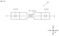
- FIG. 11A is a plan view of a current sensor 50 according to a reference example.
- FIG. 11B is a cross-sectional view of the current sensor 50 taken along line BB in FIG. 11A.
- current sensor 50 has magnetic detection unit 52 disposed opposite bus bar 51.
- Bus bar 1 of current sensor 50 has fastening portion 51A and main body portion 51B including a constricted portion facing magnetic detection unit 52, which are made of different types of metallic materials.
- the fastening portion 51A is made of Cu as the first metallic material 53
- the main body portion 51B is made of Al as the second metallic material 54. This reduces the contact resistance of the fastening portion 51A and suppresses heat generation due to the current to be measured, compared to when the fastening portion 61A and the main body portion 61B of the busbar 61 of the conventional current sensor 60 shown in FIG. 15C are made of Al. In addition, suppressing the skin effect in the busbar 51 improves the frequency characteristics of the magnetic flux density detected by the magnetic detection portion 52.
- the following table shows the frequency characteristics (phase characteristics) of Cu and Al.
- the skin depth in Table 2 is the distance at which an electromagnetic field incident on a material is attenuated to 1/e ( ⁇ 1/2.718 ⁇ -8.7 db).
- FIG. 12A is a graph showing the results of a simulation of the relationship between the frequency and phase angle of the current to be measured for a reference current sensor 50 having a bus bar 51 with a fastening portion 51A made of Cu and a body portion 51B made of Al, and a conventional current sensor 60 having a bus bar 61 with a fastening portion 61A and a body portion 61B made of Cu.
- FIG. 12B is a graph showing the results of a simulation of the relationship between the frequency of the measured current and the gain for the reference current sensor 50 shown in FIGS. 11A-11B and the conventional current sensor 60 shown in FIGS. 15A-15C.
- FIG. 13A is a graph showing the measurement results of the temperature change in the constricted portion of fastening portion 61A and main body portion 61B over time as the current to be measured is passed through a conventional current sensor 60 having a busbar 61 whose fastening portion 61A and main body portion 61B are made of Al.
- FIG. 13B is a graph showing the measurement results of the temperature change in the constricted portion of fastening portion 61A and main body portion 61B over time as the current to be measured is passed for a conventional current sensor 60 having a busbar 61 whose fastening portion 61A and main body portion 61B are made of Cu.
- FIG. 13A is a graph showing the measurement results of the temperature change in the constricted portion of fastening portion 61A and main body portion 61B over time as the current to be measured is passed through a conventional current sensor 60 having a busbar 61 whose fastening portion 61A and main body portion 61B are made of Cu.
- 13C is a graph showing the measurement results of the temperature change in the constricted portion of fastening portion 51A and main body portion 51B over time as the current to be measured flows when current is passed under the same conditions for a reference example current sensor 50 having a busbar 51 in which fastening portion 51A is made of Cu and main body portion 51B is made of Al.
- a configuration in which the fastening portion 51A is made of Cu and the main body portion 51B is made of Al is effective in reducing the delay in the detection voltage relative to the current to be measured, improving the gain, and suppressing the rise in temperature when the current to be measured flows.
- FIG. 14A is a plan view of a current sensor 50 according to another reference example.
- FIG. 14B is a cross-sectional view of the current sensor 50 taken along line BB in FIG. 14A.
- the fastening portion 51A of the busbar 51 in the current sensor 50 is configured such that the Z-axis direction surface of Al is covered with Cu, the temperature rise when the current to be measured flows can be reduced.
- the present invention is useful as a current sensor that is attached to various devices to measure the current to be measured in order to control or monitor the devices.
Landscapes
- Physics & Mathematics (AREA)
- General Physics & Mathematics (AREA)
- Measuring Instrument Details And Bridges, And Automatic Balancing Devices (AREA)
Priority Applications (4)
| Application Number | Priority Date | Filing Date | Title |
|---|---|---|---|
| EP23918522.6A EP4657081A1 (en) | 2023-01-25 | 2023-11-08 | Electric current sensor |
| CN202380085771.2A CN120344863A (zh) | 2023-01-25 | 2023-11-08 | 电流传感器 |
| JP2024572846A JPWO2024157567A1 (https=) | 2023-01-25 | 2023-11-08 | |
| US19/230,583 US20250298060A1 (en) | 2023-01-25 | 2025-06-06 | Current sensor |
Applications Claiming Priority (2)
| Application Number | Priority Date | Filing Date | Title |
|---|---|---|---|
| JP2023-009438 | 2023-01-25 | ||
| JP2023009438 | 2023-01-25 |
Related Child Applications (1)
| Application Number | Title | Priority Date | Filing Date |
|---|---|---|---|
| US19/230,583 Continuation US20250298060A1 (en) | 2023-01-25 | 2025-06-06 | Current sensor |
Publications (1)
| Publication Number | Publication Date |
|---|---|
| WO2024157567A1 true WO2024157567A1 (ja) | 2024-08-02 |
Family
ID=91970241
Family Applications (1)
| Application Number | Title | Priority Date | Filing Date |
|---|---|---|---|
| PCT/JP2023/040148 Ceased WO2024157567A1 (ja) | 2023-01-25 | 2023-11-08 | 電流センサ |
Country Status (5)
| Country | Link |
|---|---|
| US (1) | US20250298060A1 (https=) |
| EP (1) | EP4657081A1 (https=) |
| JP (1) | JPWO2024157567A1 (https=) |
| CN (1) | CN120344863A (https=) |
| WO (1) | WO2024157567A1 (https=) |
Citations (8)
| Publication number | Priority date | Publication date | Assignee | Title |
|---|---|---|---|---|
| JP2010175474A (ja) * | 2009-01-30 | 2010-08-12 | Aisin Aw Co Ltd | 電流検出装置 |
| WO2012133592A1 (ja) * | 2011-03-29 | 2012-10-04 | 三洋電機株式会社 | 電源装置及び電源装置を備える車両 |
| JP2015172531A (ja) * | 2014-03-12 | 2015-10-01 | 株式会社東海理化電機製作所 | シールド部材及びそれを用いた電流検出装置 |
| WO2017014049A1 (ja) * | 2015-07-17 | 2017-01-26 | 株式会社オートネットワーク技術研究所 | 配線モジュール、及び蓄電モジュール |
| WO2019181173A1 (ja) * | 2018-03-20 | 2019-09-26 | 株式会社デンソー | 電流センサ |
| WO2021235445A1 (ja) * | 2020-05-21 | 2021-11-25 | 株式会社オートネットワーク技術研究所 | 回路構成体 |
| WO2022118878A1 (ja) * | 2020-12-02 | 2022-06-09 | 株式会社デンソー | 電流センサ |
| JP2022100597A (ja) * | 2020-12-24 | 2022-07-06 | 株式会社アイシン | 電流センサ |
Family Cites Families (1)
| Publication number | Priority date | Publication date | Assignee | Title |
|---|---|---|---|---|
| JP6973021B2 (ja) | 2017-12-18 | 2021-11-24 | 日立金属株式会社 | 電流センサ |
-
2023
- 2023-11-08 WO PCT/JP2023/040148 patent/WO2024157567A1/ja not_active Ceased
- 2023-11-08 CN CN202380085771.2A patent/CN120344863A/zh active Pending
- 2023-11-08 EP EP23918522.6A patent/EP4657081A1/en active Pending
- 2023-11-08 JP JP2024572846A patent/JPWO2024157567A1/ja active Pending
-
2025
- 2025-06-06 US US19/230,583 patent/US20250298060A1/en active Pending
Patent Citations (8)
| Publication number | Priority date | Publication date | Assignee | Title |
|---|---|---|---|---|
| JP2010175474A (ja) * | 2009-01-30 | 2010-08-12 | Aisin Aw Co Ltd | 電流検出装置 |
| WO2012133592A1 (ja) * | 2011-03-29 | 2012-10-04 | 三洋電機株式会社 | 電源装置及び電源装置を備える車両 |
| JP2015172531A (ja) * | 2014-03-12 | 2015-10-01 | 株式会社東海理化電機製作所 | シールド部材及びそれを用いた電流検出装置 |
| WO2017014049A1 (ja) * | 2015-07-17 | 2017-01-26 | 株式会社オートネットワーク技術研究所 | 配線モジュール、及び蓄電モジュール |
| WO2019181173A1 (ja) * | 2018-03-20 | 2019-09-26 | 株式会社デンソー | 電流センサ |
| WO2021235445A1 (ja) * | 2020-05-21 | 2021-11-25 | 株式会社オートネットワーク技術研究所 | 回路構成体 |
| WO2022118878A1 (ja) * | 2020-12-02 | 2022-06-09 | 株式会社デンソー | 電流センサ |
| JP2022100597A (ja) * | 2020-12-24 | 2022-07-06 | 株式会社アイシン | 電流センサ |
Non-Patent Citations (1)
| Title |
|---|
| See also references of EP4657081A1 * |
Also Published As
| Publication number | Publication date |
|---|---|
| JPWO2024157567A1 (https=) | 2024-08-02 |
| CN120344863A (zh) | 2025-07-18 |
| US20250298060A1 (en) | 2025-09-25 |
| EP4657081A1 (en) | 2025-12-03 |
Similar Documents
| Publication | Publication Date | Title |
|---|---|---|
| JP6075784B2 (ja) | バスバー及びバスバーモジュール、並びにバスバーの製造方法 | |
| JP6973021B2 (ja) | 電流センサ | |
| JP7003609B2 (ja) | 電流センサ | |
| US20110316129A1 (en) | Multilayer structures for magnetic shielding | |
| JP6536544B2 (ja) | 電流センサ | |
| US20200381881A1 (en) | Busbar and power module with busbar | |
| WO2024157567A1 (ja) | 電流センサ | |
| CN111542758B (zh) | 多相电流测量装置和用于多相电流测量的方法 | |
| US11515801B2 (en) | Shield in a power conversion device | |
| CN104518297B (zh) | 电子部件、电部件的连接构件 | |
| US20200182912A1 (en) | Electric current sensor | |
| JP2017156319A (ja) | 電流センサユニット | |
| WO2019244749A1 (ja) | 共振器及びフィルタ | |
| WO2022219866A1 (ja) | 電流センサ | |
| JP2023042800A (ja) | 開閉機器の端子構造 | |
| US20250224429A1 (en) | Current Sensor | |
| JP2011039021A (ja) | 電流センサ | |
| JP2018018762A (ja) | フラットケーブル | |
| WO2021070833A1 (ja) | 磁気センサ及びこれを備えた電流検出装置 | |
| US11747367B2 (en) | Current sensor | |
| JP6557551B2 (ja) | 電磁波シールド材 | |
| JP2017045811A (ja) | 電磁波シールド品 | |
| JP7309646B2 (ja) | バスダクト | |
| JP6296838B2 (ja) | バスバー | |
| JP2024106418A (ja) | 位置検出装置 |
Legal Events
| Date | Code | Title | Description |
|---|---|---|---|
| 121 | Ep: the epo has been informed by wipo that ep was designated in this application |
Ref document number: 23918522 Country of ref document: EP Kind code of ref document: A1 |
|
| WWE | Wipo information: entry into national phase |
Ref document number: 2024572846 Country of ref document: JP |
|
| WWE | Wipo information: entry into national phase |
Ref document number: CN2023800857712 Country of ref document: CN Ref document number: 202380085771.2 Country of ref document: CN |
|
| WWP | Wipo information: published in national office |
Ref document number: 202380085771.2 Country of ref document: CN |
|
| NENP | Non-entry into the national phase |
Ref country code: DE |
|
| WWP | Wipo information: published in national office |
Ref document number: 2023918522 Country of ref document: EP |