WO2024154594A1 - 位相差フィルム、積層光学フィルム、光学物品、仮想現実表示装置 - Google Patents
位相差フィルム、積層光学フィルム、光学物品、仮想現実表示装置 Download PDFInfo
- Publication number
- WO2024154594A1 WO2024154594A1 PCT/JP2024/000040 JP2024000040W WO2024154594A1 WO 2024154594 A1 WO2024154594 A1 WO 2024154594A1 JP 2024000040 W JP2024000040 W JP 2024000040W WO 2024154594 A1 WO2024154594 A1 WO 2024154594A1
- Authority
- WO
- WIPO (PCT)
- Prior art keywords
- layer
- film
- retardation
- optical
- light
- Prior art date
- Legal status (The legal status is an assumption and is not a legal conclusion. Google has not performed a legal analysis and makes no representation as to the accuracy of the status listed.)
- Ceased
Links
Images


Classifications
-
- G—PHYSICS
- G02—OPTICS
- G02B—OPTICAL ELEMENTS, SYSTEMS OR APPARATUS
- G02B5/00—Optical elements other than lenses
- G02B5/30—Polarising elements
- G02B5/3083—Birefringent or phase retarding elements
-
- B—PERFORMING OPERATIONS; TRANSPORTING
- B32—LAYERED PRODUCTS
- B32B—LAYERED PRODUCTS, i.e. PRODUCTS BUILT-UP OF STRATA OF FLAT OR NON-FLAT, e.g. CELLULAR OR HONEYCOMB, FORM
- B32B7/00—Layered products characterised by the relation between layers; Layered products characterised by the relative orientation of features between layers, or by the relative values of a measurable parameter between layers, i.e. products comprising layers having different physical, chemical or physicochemical properties; Layered products characterised by the interconnection of layers
- B32B7/02—Physical, chemical or physicochemical properties
- B32B7/023—Optical properties
-
- G—PHYSICS
- G02—OPTICS
- G02B—OPTICAL ELEMENTS, SYSTEMS OR APPARATUS
- G02B1/00—Optical elements characterised by the material of which they are made; Optical coatings for optical elements
- G02B1/10—Optical coatings produced by application to, or surface treatment of, optical elements
- G02B1/11—Anti-reflection coatings
-
- G—PHYSICS
- G02—OPTICS
- G02B—OPTICAL ELEMENTS, SYSTEMS OR APPARATUS
- G02B1/00—Optical elements characterised by the material of which they are made; Optical coatings for optical elements
- G02B1/10—Optical coatings produced by application to, or surface treatment of, optical elements
- G02B1/11—Anti-reflection coatings
- G02B1/111—Anti-reflection coatings using layers comprising organic materials
-
- G—PHYSICS
- G02—OPTICS
- G02B—OPTICAL ELEMENTS, SYSTEMS OR APPARATUS
- G02B1/00—Optical elements characterised by the material of which they are made; Optical coatings for optical elements
- G02B1/10—Optical coatings produced by application to, or surface treatment of, optical elements
- G02B1/11—Anti-reflection coatings
- G02B1/118—Anti-reflection coatings having sub-optical wavelength surface structures designed to provide an enhanced transmittance, e.g. moth-eye structures
-
- G—PHYSICS
- G02—OPTICS
- G02B—OPTICAL ELEMENTS, SYSTEMS OR APPARATUS
- G02B1/00—Optical elements characterised by the material of which they are made; Optical coatings for optical elements
- G02B1/10—Optical coatings produced by application to, or surface treatment of, optical elements
- G02B1/14—Protective coatings, e.g. hard coatings
-
- G—PHYSICS
- G02—OPTICS
- G02B—OPTICAL ELEMENTS, SYSTEMS OR APPARATUS
- G02B5/00—Optical elements other than lenses
- G02B5/30—Polarising elements
-
- G—PHYSICS
- G02—OPTICS
- G02B—OPTICAL ELEMENTS, SYSTEMS OR APPARATUS
- G02B5/00—Optical elements other than lenses
- G02B5/30—Polarising elements
- G02B5/3016—Polarising elements involving passive liquid crystal elements
-
- G—PHYSICS
- G09—EDUCATION; CRYPTOGRAPHY; DISPLAY; ADVERTISING; SEALS
- G09F—DISPLAYING; ADVERTISING; SIGNS; LABELS OR NAME-PLATES; SEALS
- G09F9/00—Indicating arrangements for variable information in which the information is built-up on a support by selection or combination of individual elements
- G09F9/30—Indicating arrangements for variable information in which the information is built-up on a support by selection or combination of individual elements in which the desired character or characters are formed by combining individual elements
Definitions
- the present invention relates to a retardation film, a laminated optical film, an optical article, and a virtual reality display device.
- a reflective polarizer is a polarizer that has the function of reflecting one polarized light of incident light and transmitting the other polarized light.
- the reflected light and transmitted light by a reflective polarizer are polarized in mutually orthogonal directions.
- mutually orthogonal polarization states refer to polarization states located at antipodes on the Poincaré sphere, such as mutually orthogonal linearly polarized light, and right-handed circularly polarized light and left-handed circularly polarized light.
- Known linear reflective polarizers in which transmitted and reflected light are linearly polarized, include, for example, a film made of a stretched dielectric multilayer film as described in Patent Document 1, and a wire grid polarizer as described in Patent Document 2.
- a reflective circular polarizer in which transmitted light and reflected light are circularly polarized for example, a film having a light-reflecting layer in which a cholesteric liquid crystal phase is fixed, as described in Patent Document 3, is known.
- Reflective polarizers are used to extract only a specific polarized light from incident light or to split incident light into two polarized lights.
- LCD displays they are used as brightness enhancement films that improve light utilization efficiency by reflecting and reusing unnecessary polarized light from the backlight. They are also used as beam splitters in LCD projectors that split the light from the light source into two linearly polarized lights and supply each to the LCD panel.
- Patent Document 4 discloses an in-vehicle rearview mirror that uses a reflective polarizer to reflect light from behind.
- Patent Document 5 discloses a method of making the display smaller and thinner by placing a linear reflective polarizer and a half mirror (semi-transparent mirror) in the focusing lens system of a virtual reality display device (head-mounted display) and further placing a phase difference film that functions as a quarter-wave plate between them.
- the present invention has been made in consideration of the above problems, and the problem that the present invention aims to solve is to provide a retardation film, a laminated optical film, an optical article, and a virtual reality display device that cause less ghosting when used in a virtual reality display device, an electronic viewfinder, etc.
- a retardation film comprising an optical interference layer and a retardation layer disposed adjacent to each other in this order, the optical interference layer having a thickness of 60 nm to 110 nm, or 230 nm to 330 nm.
- the retardation film according to [1], wherein the refractive index of the optical interference layer in an in-plane direction is 1.53 to 1.59.
- a retardation film further comprising an adhesive layer, the adhesive layer, the optical interference layer, and the retardation layer being disposed adjacent to each other in this order,
- the retardation film according to any one of [1] to [3], wherein when the refractive index of the adhesive layer is nA and the average refractive index of the retardation layer is nL, the refractive index nI of the optical interference layer in the in-plane direction is (nA ⁇ nL) 1/2 -0.03 ⁇ nI ⁇ (nA ⁇ nL) 1/2 +0.03.
- the laminated optical film according to [13], wherein the antireflection layer is a moth-eye film or an AR film.
- An optical article comprising the laminated optical film according to any one of [9] to [15] and a lens.
- a virtual reality display device comprising the optical article according to [16].
- the present invention provides a retardation film, a laminated optical film, an optical article, and a virtual reality display device that produce less ghosting when used in a virtual reality display device, an electronic viewfinder, etc.
- FIG. 1 is a schematic diagram illustrating an example of a retardation film of the present invention.
- FIG. 2 is a schematic diagram showing another example of the retardation film of the present invention.
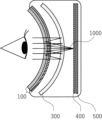
- 1 is an example of a virtual reality display device using the laminated optical film of the present invention.
- 1 is an example of a virtual reality display device using the laminated optical film of the present invention.
- 1 is a schematic diagram illustrating an example of a laminated optical film of the present invention.
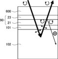
- 1A and 1B are diagrams for explaining the function of a conventional retardation film.
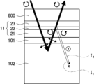
- 1A to 1C are diagrams for explaining the function of the retardation film of the present invention.
- 1 is another example of a virtual reality display device using the retardation film of the present invention.
- orthogonal does not mean strictly 90°, but means 90° ⁇ 10°, preferably 90° ⁇ 5°.
- parallel does not mean strictly 0°, but means 0° ⁇ 10°, preferably 0° ⁇ 5°.
- 45° does not mean strictly 45°, but means 45° ⁇ 10°, preferably 45° ⁇ 5°.
- absorption axis refers to the polarization direction in which the absorbance is maximum in the plane when linearly polarized light is incident.
- reflection axis refers to the polarization direction in which the reflectance is maximum in the plane when linearly polarized light is incident.
- transmission axis refers to the direction perpendicular to the absorption axis or reflection axis in the plane.
- slow axis refers to the direction in which the refractive index is maximum in the plane.
- the phase difference means the in-plane retardation and is expressed as Re( ⁇ ), where Re( ⁇ ) represents the in-plane retardation at a wavelength ⁇ , and unless otherwise specified, the wavelength ⁇ is 550 nm.
- the retardation in the thickness direction at a wavelength ⁇ is referred to as Rth( ⁇ ) in this specification, and unless otherwise specified, the wavelength ⁇ is 550 nm.
- Re( ⁇ ) and Rth( ⁇ ) can be values measured at a wavelength ⁇ using an AxoScan OPMF-1 (manufactured by Optosciences Inc.).
- the retardation film of the present invention comprises an optical interference layer and a retardation layer disposed adjacent to each other in this order, and the optical interference layer has a thickness of 60 nm to 110 nm, or 230 nm to 330 nm.
- Fig. 1 is a schematic cross-sectional view showing an example of the configuration of a retardation film 10.
- the retardation film 10 is composed of a retardation layer 21 and an optical interference layer 22, which are disposed adjacent to each other.
- the retardation film of the present invention can be used in a laminated optical film.
- the laminated optical film can be used in an optical article used in a virtual reality display device.
- the retardation film has the above configuration, and the thickness of the optical interference layer is set to satisfy the above relationship, thereby providing an anti-reflection effect.
- the retardation film of the present invention may include an adhesive layer for bonding the retardation film to a lens.
- Fig. 2 is a schematic cross-sectional view showing an example of the configuration of a retardation film 11.
- the retardation film 11 is composed of a retardation layer 21, an optical interference layer 22, and an adhesive layer 23, which are arranged adjacent to each other.
- FIG. 6 is an example in which a retardation film 90 having a retardation layer 21 and an adhesive layer 23 is laminated to a lens 600 on the adhesive layer 23 side, and a linear reflective polarizer 102 is laminated on the retardation layer 21 side via an adhesive layer 101.
- This configuration corresponds to an optical article used in a virtual reality display device described below, and is used as a reciprocating optical system (folding optical system) in combination with a half mirror.
- the upper side in FIG. 6 (lens 600 side) is the image display device side
- the lower side linear reflective polarizer 102 side) is the viewing side.
- the right-handed circularly polarized light when right-handed circularly polarized light is incident from the lens 600 side, the right-handed circularly polarized light that has passed through the lens 600 and the adhesive layer 23 is converted into linearly polarized light by the phase difference layer 21.
- the explanation will be given assuming that the light is converted into linearly polarized light in the left-right direction in the figure. This linearly polarized light passes through the adhesive layer 101 and enters the linear reflective polarizer 102.
- the linear reflective polarizer 102 reflects linearly polarized light in the left-right direction in the figure and transmits linearly polarized light perpendicular to the paper surface in the figure
- the linearly polarized light in the left-right direction that entered the linearly reflective polarizer 102 is reflected.
- the reflected linearly polarized light in the left-right direction passes through the adhesive layer 101 and enters the phase difference layer 21.
- the phase difference layer 21 converts the linearly polarized light in the left-right direction into right-handed circularly polarized light and transmits it.
- This right-handed circularly polarized light passes through the adhesive layer 23 and the lens 600.
- the transmitted light is incident on, for example, a half mirror.
- This linearly polarized light passes through the adhesive layer 101 and enters the linearly reflective polarizer 102, but since the linearly reflective polarizer 102 has a transmission axis perpendicular to the paper surface, the linearly polarized light perpendicular to the paper surface passes through the linearly reflective polarizer 102 and is emitted to the viewing side. In this way, in the conventional configuration, unnecessary light reflected at the interface is emitted to the viewing side, and is viewed as a ghost.
- FIG. 7 is an example in which a retardation film 11 having a retardation layer 21, an optical interference layer 22, and an adhesive layer 23 is laminated to a lens 600 on the adhesive layer 23 side, and a linear reflective polarizer 102 is laminated on the retardation layer 21 side via an adhesive layer 101.
- This configuration corresponds to an optical article used in a virtual reality display device described later, and is used as a reciprocating optical system (folding optical system) in combination with a half mirror.
- the upper side in FIG. 7 (lens 600 side) is the image display device side
- the lower side linear reflective polarizer 102 side) is the viewing side.
- the right-handed circularly polarized light when right-handed circularly polarized light is incident from the lens 600 side, the right-handed circularly polarized light that has passed through the lens 600, the adhesive layer 23, and the optical interference layer 22 is converted into linearly polarized light by the phase difference layer 21.
- the explanation will be given assuming that the light is converted into linearly polarized light in the left-right direction in the figure. This linearly polarized light passes through the adhesive layer 101 and enters the linear reflective polarizer 102.
- the linear reflective polarizer 102 reflects linearly polarized light in the left-right direction in the figure and transmits linearly polarized light perpendicular to the paper surface in the figure
- the linearly polarized light in the left-right direction that entered the linearly reflective polarizer 102 is reflected.
- the reflected linearly polarized light in the left-right direction passes through the adhesive layer 101 and enters the phase difference layer 21.
- the phase difference layer 21 converts the linearly polarized light in the left-right direction into right-handed circularly polarized light and transmits it.
- This right-handed circularly polarized light passes through the optical interference layer 22, the adhesive layer 23, and the lens 600.
- the transmitted light is incident, for example, on a half mirror.
- reflected light I1 in the figure a part of the right-handed circularly polarized light reflected by the linear reflective polarizer 102 and converted by the retardation layer 21 is reflected at the interface between the retardation layer 21 and the optical interference layer 22 (reflected light I1 in the figure). Another part of the right-handed circularly polarized light is also reflected at the interface between the optical interference layer 22 and the adhesive layer 23 (reflected light I2 in the figure).
- the reflected lights I1 and I2 which are right-handed circularly polarized light reflected at each interface, change in their rotation direction in the opposite direction. That is, the reflected lights I1 and I2, which are right-handed circularly polarized light reflected at the interface, change to left-handed circularly polarized light.
- the reflected lights I1 and I2 which are left-handed circularly polarized light, are converted by the retardation layer 21 into linearly polarized light in a direction perpendicular to the paper surface in the figure.
- This linearly polarized light passes through the adhesive layer 101 and enters the linearly reflective polarizer 102.
- the linearly reflective polarizer 102 has a transmission axis perpendicular to the paper surface, the linearly polarized light perpendicular to the paper surface passes through the linearly reflective polarizer 102 and is emitted to the viewing side.
- the reflected light I 1 reflected at the interface between the retardation layer 21 and the optical interference layer 22 and the reflected light I 2 reflected at the interface between the optical interference layer 22 and the adhesive layer 23 have different optical path lengths, so interference occurs.
- the reflected light I 1 and the reflected light I 2 may strengthen or weaken each other, but in the present invention, by setting the film thickness of the optical interference layer 22 to 60 nm to 110 nm or 230 nm to 330 nm, the reflected light I 1 and the reflected light I 2 weaken each other, and it is possible to suppress the unnecessary light reflected at the interface from being emitted to the viewing side, and to reduce ghosts.
- the film thickness of the optical interference layer 22 is determined taking into consideration the fact that, among the light incident on the interface from the front and oblique directions, the vicinity of the front is particularly important for interfacial reflection, that light with a wavelength of about 550 nm contributes greatly to the visibility of ghosts, and the refractive index of the optical interference layer 22, so that reflected light I1 and reflected light I2 weaken each other near the front and near a wavelength of 550 nm, i.e., so that the phases of reflected light I1 and reflected light I2 are shifted by approximately ⁇ /2 or approximately 3 ⁇ /2.
- the retardation layer used in the present invention is a retardation plate having a function of converting linearly polarized light of a certain wavelength into circularly polarized light (or circularly polarized light into linearly polarized light). More specifically, it is a plate exhibiting an in-plane retardation Re of ⁇ /4 (or an odd multiple thereof) at a certain wavelength ⁇ nm.
- the in-plane retardation (Re(550)) of the retardation layer at a wavelength of 550 nm may have an error of about 25 nm around the ideal value (137.5 nm), and is preferably 110 to 160 nm, and more preferably 120 to 150 nm.
- the retardation layer used in the present invention preferably exhibits the characteristics of a ⁇ /4 plate at each wavelength in the visible light range, and such a retardation layer is particularly called a broadband ⁇ /4 plate. It is preferable that the in-plane retardation (Re( ⁇ )) of the broadband ⁇ /4 plate at a wavelength of ⁇ nm satisfies the following formulas (A) and (B).
- Re(450) represents the in-plane retardation of a ⁇ /4 plate at a wavelength of 450 nm
- Re(550) represents the in-plane retardation of a ⁇ /4 plate at a wavelength of 550 nm
- Re(650) represents the in-plane retardation of a ⁇ /4 plate at a wavelength of 650 nm.
- the retardation layer used in the present invention may be composed of a single retardation layer, or may be composed of two or more retardation layers laminated by lamination, sequential formation, or other methods.
- the retardation layer here is a layer that exhibits optical anisotropy.
- Examples of the retardation layer include layers in which at least two of nx, ny, and nz are different.
- nx represents the refractive index in the direction perpendicular to the thickness direction of the retardation layer (in-plane direction) and in the direction that gives the maximum refractive index.
- ny represents the refractive index in the in-plane direction of the retardation layer and perpendicular to the direction of nx.
- nz represents the refractive index in the thickness direction of the retardation layer.
- the material constituting the retardation layer used in the present invention is not particularly limited, and examples thereof include liquid crystal compounds and polymers.
- a liquid crystal compound can form a retardation layer by orienting a liquid crystal material to exhibit refractive index anisotropy.
- a polymer can form a retardation layer by exhibiting refractive index anisotropy through stretching a polymer film obtained by casting, coating, or the like.
- the retardation layer used in the present invention is preferably a layer formed using a liquid crystal compound, and more preferably a layer formed using a liquid crystal compound having a polymerizable group.
- liquid crystal compound is not particularly limited.
- liquid crystal compounds can be classified into rod-shaped type (rod-shaped liquid crystal compounds) and disk-shaped type (discotic liquid crystal compounds) based on their shape.
- liquid crystal compounds can be classified into low molecular type and polymer type.
- Polymer generally refers to a compound with a degree of polymerization of 100 or more (Polymer Physics, Phase Transition Dynamics, Masao Doi, p. 2, Iwanami Shoten, 1992).
- any liquid crystal compound can be used, but it is preferable to use rod-shaped liquid crystal compounds or discotic liquid crystal compounds, and it is more preferable to use rod-shaped liquid crystal compounds.
- rod-shaped liquid crystal compounds Two or more rod-shaped liquid crystal compounds, two or more discotic liquid crystal compounds, or a mixture of rod-shaped liquid crystal compounds and discotic liquid crystal compounds may be used.
- rod-shaped liquid crystal compound examples include the liquid crystal compounds described in claim 1 of JP-T-11-513019 and paragraphs 0026 to 0098 of JP-A-2005-289980.
- discotic liquid crystal compound examples include the liquid crystal compounds described in paragraphs 0020 to 0067 of JP-A-2007-108732 and paragraphs 0013 to 0108 of JP-A-2010-244038.
- the liquid crystal compound preferably has a polymerizable group. That is, the liquid crystal compound is preferably a polymerizable liquid crystal compound. When the liquid crystal compound has a polymerizable group, the alignment state of the liquid crystal compound can be easily fixed by a curing treatment described later.
- the type of polymerizable group possessed by the liquid crystal compound is not particularly limited, and is preferably a functional group capable of an addition polymerization reaction, more preferably a polymerizable ethylenically unsaturated group or a ring-polymerizable group, and further preferably a (meth)acryloyl group, a vinyl group, a styryl group, or an allyl group.
- the number of polymerizable groups that the liquid crystal compound has is not particularly limited, but is preferably at least 2. The upper limit is not particularly limited, but is often 10 or less.
- the liquid crystal compound may be either a liquid crystal compound that shows normal wavelength dispersion or reverse wavelength dispersion.
- the liquid crystal compound that shows reverse wavelength dispersion is preferable, and the liquid crystal compound that has two or more polymerizable groups and shows reverse wavelength dispersion is more preferable.
- a "liquid crystal compound exhibiting reverse wavelength dispersion” refers to a compound that satisfies the relationship between the above-mentioned formulas (A) and (B) when the in-plane retardation (Re) value at a specific wavelength (visible light range) of an optically anisotropic layer prepared using this compound is measured.
- liquid crystal compound exhibiting normal wavelength dispersion refers to a compound that satisfies the relationship between the following formulas (C) and (D) when the in-plane retardation (Re) value at a specific wavelength (visible light range) of a retardation layer prepared using this compound is measured.
- the retardation layer is preferably a layer formed using a liquid crystal compound having a polymerizable group, and more preferably a layer formed by fixing the orientation state of the liquid crystal compound having a polymerizable group.
- the orientation state that the liquid crystal compound having a polymerizable group can take is not particularly limited, and examples thereof include homogeneous orientation, homeotropic orientation, twisted orientation, cholesteric orientation, hybrid orientation (orientation in which the tilt angle of the liquid crystal compound changes continuously from one surface to the other surface), and tilted orientation (orientation in which the tilt angle of the liquid crystal compound is constant from one surface to the other surface).
- the twisted orientation refers to an orientation state in which the liquid crystal compound is twisted with the thickness direction as the axis of rotation, and when the liquid crystal compound is twisted and has a predetermined tilt angle (tilt angle is greater than 0°), it corresponds to a twisted hybrid orientation.
- the twisted orientation corresponds to an embodiment in which the twist angle of the liquid crystal compound is less than 360°
- the cholesteric orientation corresponds to an embodiment in which the twist angle of the liquid crystal compound is 360° or more.
- the "fixed" state is the most typical and preferred state in which the alignment of the liquid crystal compound is maintained, but is not limited thereto.
- the layer has no fluidity and the alignment is not changed by an external field or force in a temperature range of usually 0 to 50° C., or in a more severe condition of ⁇ 30 to 70° C., and that the fixed alignment can be stably maintained.
- the retardation layer formed using a liquid crystal compound may have a plurality of regions along the thickness direction in which the liquid crystal compound has different alignment states.
- the retardation layer may have a region in which the liquid crystal compound is fixed in a homogeneous alignment state and a region in which the liquid crystal compound is fixed in a twisted alignment state along the thickness direction.
- the thickness of the retardation layer is not particularly limited, but is preferably 0.1 to 10.0 ⁇ m, and more preferably 0.5 to 5.0 ⁇ m.
- a wideband ⁇ /4 plate examples include a single-layer retardation layer, such as a retardation layer using a liquid crystal compound exhibiting reverse wavelength dispersion, as disclosed in International Publication WO2019/160016, JP 2020-173460, International Publication WO2021/157694, etc., and a retardation layer having multiple regions along the thickness direction in which the orientation state of the liquid crystal compound is different, as disclosed in International Publication WO2022/030308, JP 2022-184691, etc.
- Examples of a laminate of two or more retardation layers include a combination of a ⁇ /4 retardation layer and a ⁇ /2 retardation layer as disclosed in JP 2001-108825 A, JP 2001-091741 A, International Publication WO 2013/137464 A, etc., and a combination of a retardation layer having a twisted orientation and another retardation layer as disclosed in JP 2001-021720 A, JP 2014-209219 A, International Publication WO 2022/255105 A, etc.
- other retardation layers such as a positive C plate and a negative C plate may be added to compensate for the phase difference change due to the oblique incident light.
- the retardation film of the present invention includes a light interference layer.
- the light interference layer may be a single light interference layer, or may be formed by laminating two or more light interference layers by a method such as lamination or successive formation.
- the thickness of the single optical interference layer is preferably in the range of 60 nm to 110 nm or 230 nm to 330 nm, more preferably in the range of 75 nm to 100 nm or 245 nm to 300 nm, and most preferably in the range of 80 nm to 95 nm or 260 nm to 285 nm.
- the refractive index of the optical interference layer is preferably 1.50 to 1.70, and more preferably 1.53 to 1.59.
- the preferred range of the optical interference layer can be generalized using the average refractive index of the adhesive layer and retardation layer, and it is preferable to satisfy the following condition.
- the refractive index nI of the optical interference layer is preferably (nA ⁇ nL) 1/2 -0.03 ⁇ nI ⁇ (nA ⁇ nL) 1/2 +0.03, more preferably (nA ⁇ nL) 1/2 -0.02 ⁇ nI ⁇ (nA ⁇ nL) 1/2 +0.02, and most preferably (nA ⁇ nL) 1/2 -0.01 ⁇ nI ⁇ (nA ⁇ nL) 1/2 +0.01.
- the refractive index of the optical interference layer By setting the refractive index of the optical interference layer within this range, it is possible to make the amplitude reflectance on both sides of the optical interference layer approximately equal, which is believed to provide a significant anti-reflection effect. This makes it possible to suppress reflected light caused by interface reflection. Reflected light whose rotation direction has been changed by interface reflection is one of the causes of ghosting, so it is believed that suppressing interface reflection can suppress the occurrence of ghosting.
- the refractive indexes of the optical interference layer, the retardation layer, and the adhesive layer can be measured by referring to the method described in the Examples.
- the optical interference layer When forming the optical interference layer, it may be formed on the retardation layer, or the optical interference layer may be formed on the temporary support first, and then the retardation layer may be formed on the retardation layer.
- Materials for forming the optical interference layer include a hard coat material crosslinked with a monomer, a photo-alignment film, and a C plate using a liquid crystal material.
- the photo-alignment film is more preferable because it also plays a role in aligning the liquid crystal when a retardation layer is formed on the optical alignment film using a liquid crystal material.
- the C plate is more preferable because it also plays a role in adjusting optical compensation.
- a positive C plate is more preferable.
- the positive C plate is a retardation layer having Re substantially zero and Rth having a negative value.
- the positive C plate can be obtained, for example, by vertically aligning a rod-shaped liquid crystal compound.
- the manufacturing method of the positive C plate refer to, for example, JP-A-2017-187732, JP-A-2016-053709, JP-A-2015-200861, etc.
- optical alignment film material As the optical interference layer, it is also a preferred embodiment to use a so-called optical alignment film (optical alignment layer) in which an optical alignment material is irradiated with polarized or non-polarized light to form an alignment layer. It is preferred to impart an alignment control force to the optical alignment film by a process of irradiating polarized light from a vertical or oblique direction, or a process of irradiating non-polarized light from an oblique direction. By using the photo-alignment film, it is possible to horizontally align a specific liquid crystal compound with excellent symmetry.
- the retardation layer positive A plate formed by using the photo-alignment film is useful for optical compensation in a liquid crystal display device that does not require a pre-tilt angle of the driving liquid crystal, such as an IPS (In-Place-Switching) mode liquid crystal display device.
- IPS In-Place-Switching
- photo-alignment materials used in the photo-alignment film include those described in JP-A-2006-285197, JP-A-2007-076839, JP-A-2007-138138, JP-A-2007-094071, JP-A-2007-121721, JP-A-2007-140465, JP-A-2007-156439, Azo compounds described in JP-A-2007-133184, JP-A-2009-109831, Japanese Patent No.
- 4205195 and 4205198 include photo-crosslinkable polyimides, polyamides, or esters described in JP-T-2003-520878, JP-T-2004-529220, and JP-T-4162850, and photo-dimerizable compounds described in JP-A-9-118717, JP-T-10-506420, JP-T-2003-505561, WO 2010/150748, JP-A-2013-177561, and JP-A-2014-012823, in particular cinnamate compounds, chalcone compounds, and coumarin compounds.
- Particularly preferred examples include azo compounds, photocrosslinkable polyimides, polyamides, esters, cinnamate compounds, and chalcone compounds.
- the optical interference layer preferably contains a material for an interlayer optical alignment film. This allows liquid crystal alignment when a liquid crystal material is applied onto the optical interference layer, and a structure in which the optical interference layer and the optical reflection layer are adjacent to each other can be formed.
- the material for the interlayer optical alignment film the optical alignment polymer described in JP-A-2021-143336 can be used.
- the material for the interlayer photo-alignment film is preferably a compound having a cinnamoyl group.
- the cinnamoyl compound is preferably contained between the optical interference layer (preferably a C-plate) and the retardation layer. That is, the cinnamoyl compound is preferably contained in the region near the boundary between the optical interference layer (preferably a C-plate) and the retardation layer.
- the adhesive layer can be made of any known adhesive or pressure-sensitive adhesive, etc., as long as it has a refractive index that satisfies the above-mentioned relational expression.
- the adhesive and/or pressure-sensitive adhesive used in the laminated optical film described below can be used as appropriate.
- the adhesive used in the adhesive layer can be any commercially available adhesive, but from the viewpoint of thinning and reducing the surface roughness Ra, the thickness is preferably 25 ⁇ m or less, more preferably 15 ⁇ m or less, and most preferably 6 ⁇ m or less.
- the adhesive is one that does not easily generate outgassing.
- the adhesive used in the adhesive layer may be any commercially available adhesive, such as an epoxy resin adhesive or an acrylic resin adhesive. From the viewpoint of thinning and reducing the surface roughness Ra of the linear reflective polarizer used in the laminated optical film, the adhesive has a thickness of preferably 25 ⁇ m or less, more preferably 5 ⁇ m or less, and most preferably 1 ⁇ m or less.
- the adhesive has a viscosity of preferably 300 cP or less, more preferably 100 cP or less.
- the pressure-sensitive adhesive and adhesive can be selected with appropriate viscoelasticity or thickness so as to bury the surface irregularities of the layer to be adhered, from the viewpoint of reducing the surface roughness Ra of the linear reflection polarizer used in the laminated optical film. From the viewpoint of burying the surface irregularities, the pressure-sensitive adhesive and adhesive preferably have a viscosity of 50 cP or more.
- the thickness is preferably thicker than the height of the surface irregularities.
- a method for adjusting the viscosity of the adhesive for example, a method of using an adhesive containing a solvent can be mentioned.
- the viscosity of the adhesive can be adjusted by changing the ratio of the solvent.
- the thickness of the adhesive can be further reduced by drying the solvent after applying the adhesive to the adherend.
- the adhesive or adhesive used for bonding each layer has a small refractive index difference with the adjacent layer. Since the retardation layer has birefringence, the refractive index in the fast axis direction and the slow axis direction are different, and when the refractive index of the liquid crystal layer is the average refractive index n ave of the liquid crystal layer, the difference between the refractive index of the adjacent adhesive layer or adhesive layer and the n ave is preferably 0.075 or less, more preferably 0.05 or less, and even more preferably 0.025 or less.
- the refractive index of the adhesive or adhesive can be adjusted, for example, by mixing titanium oxide fine particles and zirconia fine particles.
- the adhesive layer between each layer has a thickness of 100 nm or less.
- the thickness of the adhesive layer is more preferably 50 nm or less, and even more preferably 30 nm or less.
- a method for forming an adhesive layer having a thickness of 100 nm or less for example, a method of depositing a ceramic adhesive such as silicon oxide (SiOx layer) on the bonding surface can be mentioned.
- the bonding surface of the bonding member can be subjected to a surface modification treatment such as plasma treatment, corona treatment, saponification treatment, etc.
- an adhesive layer having a thickness of 100 nm or less can be provided by the procedure shown in (1) to (3) below.
- the layers to be laminated are attached to a temporary support made of a glass substrate.
- a SiOx layer having a thickness of 100 nm or less is formed by deposition or the like.
- the deposition can be performed using, for example, a deposition device (model number ULEYES) manufactured by ULVAC, Inc., using SiOx powder as a deposition source.
- the surface of the formed SiOx layer is also preferable to subject the surface of the formed SiOx layer to a plasma treatment.
- the temporary support is peeled off. The bonding is preferably performed at a temperature of, for example, 120°C.
- the coating, adhesion or lamination of each layer may be performed by a roll-to-roll method or a sheet-fed method.
- the roll-to-roll method is preferable from the viewpoints of improving productivity and reducing axial misalignment of each layer.
- the single-wafer system is preferable in that it is suitable for small-lot, high-mix production and that it allows the selection of a special bonding method such as one that results in an adhesive layer having a thickness of 100 nm or less, as described above.
- Methods for applying the adhesive to the adherend include known methods such as roll coating, gravure printing, spin coating, wire bar coating, extrusion coating, direct gravure coating, reverse gravure coating, die coating, spraying, and inkjet printing.
- the retardation film of the present invention may include a support and an orientation layer, but the support and the orientation layer may be a temporary support that is peeled off and removed when preparing the laminated optical film described later.
- the retardation film is transferred to another laminated optical film, and then the temporary support is peeled off and removed, so that the laminated optical film can be made thin, and further, the retardation of the temporary support can be prevented from adversely affecting the polarization degree of transmitted light, which is preferable.
- the type of the support is not particularly limited, but is preferably transparent to visible light, and for example, films of cellulose acylate, polycarbonate, polysulfone, polyethersulfone, polyacrylate and polymethacrylate, cyclic polyolefin, polyolefin, polyamide, polystyrene, polyester, etc. can be used. Among them, cellulose acylate film, cyclic polyolefin, polyacrylate, or polymethacrylate is preferable. In addition, commercially available cellulose acetate films (for example, "TD80U” and "Z-TAC” manufactured by Fujifilm Corporation) can also be used.
- the support When the support is a temporary support, it is preferable to use a support having high tear strength in order to prevent breakage during peeling, such as polycarbonate and polyester films.
- the support preferably has a small phase difference from the viewpoint of suppressing the adverse effect on the polarization degree of transmitted light.
- the magnitude of Re at 550 nm is preferably 10 nm or less
- the absolute value of the magnitude of Rth is preferably 50 nm or less. Even if the support is used as the above-mentioned temporary support, it is preferable that the phase difference of the temporary support is small in performing quality inspection of the retardation film and the laminated optical film in the manufacturing process of the laminated optical film described later.
- the retardation film used in the laminated optical film described below is transparent to near-infrared light.
- the laminated optical film of the present invention preferably has at least a retardation film that converts circularly polarized light into linearly polarized light, and a linear reflective polarizer, in this order.
- the retardation film the above-mentioned retardation film is used.
- the preferred embodiment of the retardation film is as described above.
- the linear reflective polarizer is preferably disposed on the retardation layer on the opposite side to the optical interference layer.
- the laminated optical film of the present invention As a suitable example of the use of the laminated optical film of the present invention, a virtual reality display device using the laminated optical film of the present invention will be taken up, and the function of the laminated optical film of the present invention will be described in detail.
- FIG. 3 is a schematic diagram of a virtual reality display device using the laminated optical film of the present invention.
- the laminated optical film 100 having the above-mentioned retardation film and linear reflection polarizer, the half mirror 300, the circular polarizing plate 400, and the image display panel 500 are arranged in order from the viewing side.
- the light ray 1000 emitted from the image display panel 500 passes through the circular polarizing plate 400 to become circularly polarized light, and passes through the half mirror 300.
- the light is converted into linearly polarized light parallel to the reflection axis of the linear reflection polarizer, and then reflected by the linear reflection polarizer.
- the polarization state of the light ray 1000 is circularly polarized light with a rotation direction opposite to that of the circularly polarized light when it entered the laminated optical film 100 the first time due to reflection by the half mirror.
- this polarized light passes through the retardation film of the laminated optical film, it is converted into linearly polarized light parallel to the transmission axis of the linearly reflective polarizer.
- FIG. 4 is a schematic diagram for explaining a case where a ghost occurs in the virtual reality display device shown in FIG. 3.
- FIG. 4 it is a schematic diagram showing a case where, when a light ray 2000 is incident on the laminated optical film 100 for the first time in a virtual reality display device, the light ray is not reflected but transmitted to the half mirror, resulting in leakage light.
- FIG. 4 when a light ray 2000 is incident on the laminated optical film 100 for the first time, the light ray is not reflected but transmitted to the half mirror, resulting in leakage light, as can be seen from FIG. 4, the user will see an image that is not magnified. This image is called a ghost or the like, and it is required to be suppressed.
- the laminated optical film 100 of the present invention has a high degree of polarization, leakage of transmitted light (i.e., ghost) when a light beam is incident on the laminated optical film 100 for the first time can be reduced.
- the laminated optical film 100 of the present invention has a high degree of polarization even for transmitted light, it is possible to increase the transmittance when a light ray is incident on the laminated optical film 100 for the second time, thereby improving the brightness of the virtual image and further suppressing coloring of the virtual image.
- the laminated optical film 100 is preferably curved, as shown in Figures 3 and 4.
- the laminated optical film 100 may be curved by forming the laminated optical film 100 itself into a curved shape, or may be curved by laminating it onto the surface of a member having a curved surface, such as a lens 600, as shown in Figure 8.
- FIG. 5 An example of the layer structure of the laminated optical film 100 of the present invention is shown in Fig. 5.
- a retardation film 11 an adhesive layer 101, a linear reflective polarizer 102, an adhesive layer 103, and a linear polarizer 104 are arranged in this order.
- the retardation film 11 has a retardation layer 21, an optical interference layer 22, and an adhesive layer 23.
- the linear polarizer 104 is preferably an absorptive linear polarizer.
- the laminated optical film of the present invention has, in this order, the retardation layer 11 that converts circularly polarized light into linearly polarized light, the linear reflective polarizer 102, and the linear polarizer 104, and therefore the transmitted light from the linear reflective polarizer 102 can be absorbed by the linear polarizer. Therefore, the degree of polarization of the transmitted light can be increased.
- the laminated optical film of the present invention preferably has a surface roughness Ra of 100 nm or less. If Ra is small, for example, when the laminated optical film is used in a virtual reality display device or the like, the sharpness of the image can be improved.
- the present inventors presume that when light is reflected in the laminated optical film, if there are irregularities, the angle of the reflected light is distorted, leading to image distortion and blurring.
- the Ra of the laminated optical film is more preferably 50 nm or less, even more preferably 30 nm or less, and particularly preferably 10 nm or less.
- the laminated optical film of the present invention is produced by laminating a large number of layers.
- each layer of the laminated optical film of the present invention preferably has Ra of 50 nm or less, more preferably 30 nm or less, and even more preferably 10 nm or less. From the viewpoint of improving the image sharpness of a reflected image, it is particularly preferable that the Ra of the linear reflective polarizer is small.
- the surface roughness Ra can be measured, for example, using a non-contact surface/layer cross-sectional shape measuring system VertScan (manufactured by Ryoka Systems Co., Ltd.).
- Vertscan is a surface shape measuring method that utilizes the phase of reflected light from a sample
- the reflected light from inside the film may overlap, making it difficult to accurately measure the surface shape.
- a metal layer may be formed on the surface of the sample to increase the reflectance of the surface and further suppress reflection from the inside.
- a sputtering method is used as a method for forming a metal layer on the surface of the sample.
- Au, Al, Pt, etc. are used as materials to be sputtered.
- the laminated optical film of the present invention preferably has a small number of point defects per unit area. Since the laminated optical film of the present invention is produced by laminating a large number of layers, in order to reduce the number of point defects in the laminated optical film as a whole, it is preferable that the number of point defects in each layer is also small. Specifically, the number of point defects in each layer is preferably 20 or less per square meter, more preferably 10 or less, and even more preferably 1 or less. In the laminated optical film as a whole, the number of point defects is preferably 100 or less per square meter, more preferably 50 or less, and even more preferably 5 or less.
- Point defects lead to a decrease in the degree of polarization of transmitted light and a decrease in image sharpness, and therefore it is preferable that there are as few point defects as possible.
- point defects include foreign matter, scratches, stains, film thickness variations, alignment defects of liquid crystal compounds, and the like.
- the number of point defects is preferably counted as the number of point defects having a size of 100 ⁇ m or more, more preferably 30 ⁇ m or more, and most preferably 10 ⁇ m or more.
- various sensors that use near-infrared light as a light source such as for eye tracking, facial expression recognition, and iris authentication, may be incorporated into the optical systems of virtual reality display devices and electronic viewfinders, and in order to minimize the effects on the sensors, it is preferable that the laminated optical film of the present invention is transparent to near-infrared light.
- the linear polarizer used in the laminated optical film of the present invention is preferably an absorption type linear polarizer.
- the absorption type linear polarizer absorbs linearly polarized light in the absorption axis direction of the incident light and transmits linearly polarized light in the transmission axis direction.
- a general polarizer can be used, for example, a polarizer in which a dichroic material is dyed and stretched on polyvinyl alcohol or other polymer resin, or a polarizer in which a dichroic material is oriented by utilizing the orientation of a liquid crystal compound, may be used.
- a polarizer in which polyvinyl alcohol is dyed with iodine and stretched is preferable.
- the thickness of the linear polarizer is preferably 10 ⁇ m or less, more preferably 7 ⁇ m or less, and even more preferably 5 ⁇ m or less.
- the single plate transmittance of the linear polarizer is preferably 40% or more, more preferably 42% or more.
- the degree of polarization is preferably 90% or more, more preferably 95% or more, and even more preferably 99% or more.
- the single plate transmittance and degree of polarization of the linear polarizer are measured using an automatic polarizing film measuring device: VAP-7070 (manufactured by JASCO Corporation).
- VAP-7070 automatic polarizing film measuring device
- the direction of the transmission axis of the linear polarizer preferably coincides with the direction of the polarization axis of the light converted into linearly polarized light by the retardation layer.
- the angle between the transmission axis of the linear polarizer and the slow axis of the retardation layer is preferably about 45°.
- the linear polarizer used in the laminated optical film of the present invention is also preferably a light-absorption anisotropic layer containing a liquid crystal compound and a dichroic substance.
- a linear polarizer containing a liquid crystal compound and a dichroic substance is preferable because it can be thinned and is unlikely to crack or break even when stretched and molded.
- the thickness of the light-absorption anisotropic layer is not particularly limited, but is preferably 0.1 to 8 ⁇ m, more preferably 0.3 to 5 ⁇ m, from the viewpoint of thinning.
- a linear polarizer containing a liquid crystal compound and a dichroic substance can be produced, for example, by referring to JP-A-2020-023153, etc. From the viewpoint of improving the polarization degree of the linear polarizer, the light absorption anisotropic layer preferably has an orientation degree of the dichroic substance of 0.95 or more, more preferably 0.97 or more.
- the liquid crystal compound contained in the composition for forming an optically absorptive anisotropic layer for forming the optically absorptive anisotropic layer is preferably a liquid crystal compound that does not exhibit dichroism in the visible range.
- the liquid crystal compound either a low molecular weight liquid crystal compound or a polymeric liquid crystal compound can be used.
- the term “low molecular weight liquid crystal compound” refers to a liquid crystal compound that does not have a repeating unit in its chemical structure.
- polymeric liquid crystal compound refers to a liquid crystal compound that has a repeating unit in its chemical structure. Examples of the polymer liquid crystal compound include the thermotropic liquid crystal polymer described in JP 2011-237513 A.
- the polymer liquid crystal compound preferably has a crosslinkable group (e.g., an acryloyl group or a methacryloyl group) at the end.
- the liquid crystal compounds may be used alone or in combination of two or more. It is also preferable to use a high molecular weight liquid crystal compound and a low molecular weight liquid crystal compound in combination.
- the content of the liquid crystal compound is preferably 25 to 2000 parts by mass, more preferably 33 to 1000 parts by mass, and even more preferably 50 to 500 parts by mass, relative to 100 parts by mass of the content of the dichroic substance in the composition. When the content of the liquid crystal compound is within the above range, the degree of orientation of the polarizer is further improved.
- the dichroic substance contained in the composition for forming an optically absorptive anisotropic layer for forming an optically absorptive anisotropic layer is not particularly limited, and examples thereof include visible light absorbing substances (dichroic dyes), ultraviolet absorbing substances, infrared absorbing substances, nonlinear optical substances, carbon nanotubes, and the like. Any conventionally known dichroic substance (dichroic dye) can be used. In the present invention, two or more dichroic substances may be used in combination.
- the linear polarizer When the linear polarizer is made of a light-absorbing anisotropic layer containing a liquid crystal compound and a dichroic substance, the linear polarizer may include a support, an orientation layer, etc., but the support and the orientation layer may be a temporary support that is peeled off and removed when preparing a laminated optical film.
- the light-absorbing anisotropic layer When a temporary support is used, the light-absorbing anisotropic layer is transferred to another laminate, and then the temporary support is peeled off and removed, so that the laminated optical film can be made thin, and further, the retardation of the temporary support can be eliminated, which is preferable because it can eliminate the adverse effect on the polarization degree of transmitted light.
- the type of the support is not particularly limited, but is preferably transparent to visible light, and for example, the same support as the support used as the retardation layer can be used.
- a preferred embodiment of the support used in the linear polarizer is the same as the preferred embodiment of the support used as the retardation layer.
- the linear polarizer used in the laminated optical film of the present invention is preferably transparent to near-infrared light.
- the laminated optical film of the present invention may have other functional layers in addition to the retardation film, the linear reflective polarizer, and the linear polarizer.
- the other functional layers are transparent to near-infrared light.
- the laminated optical film of the present invention further has a positive C plate.
- the positive C plate is a retardation layer having Re substantially zero and Rth having a negative value.
- the positive C plate can be obtained, for example, by vertically aligning a rod-shaped liquid crystal compound.
- the positive C plate functions as an optical compensation layer for increasing the degree of polarization of transmitted light with respect to obliquely incident light.
- the positive C plate may be disposed at any position in the laminated optical film, and a plurality of positive C plates may be disposed.
- the positive C plate may be disposed adjacent to the retardation film or inside the retardation film.
- the retardation layer has a positive Rth.
- the change in the polarization state of the obliquely incident light can be further suppressed, and the decrease in the degree of polarization of the transmitted light can be further suppressed, and as a result, ghosts can be further suppressed, which is preferable.
- the positive C plate is preferably disposed between the lens and the retardation film, but may be disposed between the retardation film and the linear reflective polarizer, or may be disposed in another location.
- the Re(550) of the positive C plate is preferably about 10 nm or less, and the Rth(550) is preferably -90 to -40 nm.
- the laminated optical film of the present invention has an anti-reflection layer on the surface.
- the laminated optical film of the present invention has a function of reflecting a specific circularly polarized light and transmitting a circularly polarized light perpendicular thereto, but the reflection on the surface of the laminated optical film generally includes the reflection of unintended polarized light, which may reduce the polarization degree of the transmitted light. Therefore, it is preferable that the laminated optical film has an anti-reflection layer on the surface.
- the anti-reflection layer may be installed only on one surface of the laminated optical film, or on both surfaces.
- the type of the anti-reflection layer is not particularly limited, but from the viewpoint of further reducing the reflectance, a moth-eye film or an AR (anti-reflective) film is preferable.
- a moth-eye film and the AR film known ones can be used.
- the laminated optical film is stretched or molded, a moth-eye film is preferred because it can maintain high antireflection performance even if the film thickness varies due to stretching.
- the peak temperature of the glass transition temperature Tg of the support is preferably 170° C. or less, more preferably 130° C. or less, from the viewpoint of facilitating stretching and molding.
- a PMMA film is preferred.
- the laminated optical film of the present invention further has a second retardation layer.
- the laminated optical film may include a retardation film, a linear reflective polarizer, a linear polarizer, and a second retardation layer in this order.
- the second retardation layer is preferably one that converts linearly polarized light into circularly polarized light, and is preferably a retardation layer having an Re of, for example, a quarter wavelength, for the reasons described below.
- the light that is incident on the laminated optical film from the side of the retardation film and transmitted through the linear reflective polarizer and the linear polarizer is linearly polarized light, a part of which is reflected at the outermost surface on the side of the linear polarizer and is again emitted from the surface on the side of the retardation film.
- Such light is unnecessary reflected light and can be a factor in reducing the degree of polarization of the reflected light, so it is preferable to reduce it.
- the second retardation layer has substantially reverse dispersion.
- the laminated optical film of the present invention may further have a support (resin substrate).
- the support can be installed at any location, and for example, when the retardation film, the linear reflective polarizer, or the linear polarizer is a film to be transferred from a temporary support, the support can be used as the transfer destination.
- the type of the support is not particularly limited, but is preferably transparent to visible light, and for example, a film of cellulose acylate, polycarbonate, polysulfone, polyethersulfone, polyacrylate, polymethacrylate, cyclic polyolefin, polyolefin, polyamide, polystyrene, polyester, etc. can be used.
- a cellulose acylate film, a cyclic polyolefin, polyacrylate, or polymethacrylate is preferable.
- a commercially available cellulose acetate film for example, "TD80U” and "Z-TAC” manufactured by Fujifilm Corporation
- the support preferably has a small retardation from the viewpoint of suppressing adverse effects on the polarization degree of transmitted light and from the viewpoint of facilitating optical inspection of the laminated optical film.
- the magnitude of Re is preferably 10 nm or less
- the absolute value of the magnitude of Rth is preferably 50 nm or less.
- the support preferably has a peak temperature of loss tangent tan ⁇ of 170°C or less.
- the peak temperature of tan ⁇ is preferably 150°C or less, and more preferably 130°C or less.
- a variety of resin substrates can be used as the support having a tan ⁇ peak temperature of 170°C or less, without any particular restrictions.
- Examples include polyolefins such as polyethylene, polypropylene, and norbornene polymers; cyclic olefin resins; polyvinyl alcohol; polyethylene terephthalate; acrylic resins such as polymethacrylic acid esters and polyacrylic acid esters; polyethylene naphthalate; polycarbonate; polysulfone; polyethersulfone; polyetherketone; polyphenylene sulfide, and polyphenylene oxide.
- polyolefins such as polyethylene, polypropylene, and norbornene polymers
- cyclic olefin resins such as polyvinyl alcohol; polyethylene terephthalate; acrylic resins such as polymethacrylic acid esters and polyacrylic acid esters; polyethylene naphthalate; polycarbonate; polysulfone; polyethersulfone
- cyclic olefin resins polyethylene terephthalate, and acrylic resins are preferred, as they are easily available on the market and have excellent transparency, and cyclic olefin resins and polymethacrylic acid esters are particularly preferred.
- resin substrates include Technoloy S001G, Technoloy S014G, Technoloy S000, Technoloy C001, Technoloy C000 (Sumika Acrylic Sales Co., Ltd.), Lumirror U Type, Lumirror FX10, Lumirror SF20 (Toray Industries, Inc.), HK-53A (Higashiyama Films Co., Ltd.), Teflex FT3 (Teijin DuPont Films Co., Ltd.), S-Cina and SCA40 (Sekisui Chemical Co., Ltd.), Zeonor Film (Optes Co., Ltd.), and Arton Film (JSR Corporation).
- the thickness of the support is not particularly limited, but is preferably 5 to 300 ⁇ m, more preferably 5 to 100 ⁇ m, and even more preferably 5 to 30 ⁇ m.
- the laminated optical film may have layers other than the above-mentioned layers, such as a pressure-sensitive adhesive layer formed by a pressure-sensitive adhesive described below, an adhesive layer formed by an adhesive described below, and a refractive index adjustment layer.
- a refractive index adjustment layer having a smaller difference in refractive index between the fast axis direction and the slow axis direction than the retardation layer may be provided between the retardation layer and the adhesive, or between the retardation layer and the adhesive.
- the refractive index adjustment layer has a layer formed by fixing the alignment state of cholesteric liquid crystal. By having the refractive index adjustment layer, it is possible to further suppress the interface reflection and the occurrence of ghosts.
- the average refractive index of the refractive index adjustment layer is smaller than the average refractive index of the retardation layer.
- the laminated optical film of the present invention is a laminate consisting of a number of layers.
- Each layer can be bonded by any bonding method, for example, a pressure sensitive adhesive, a bonding agent, or the like.
- the adhesive any commercially available adhesive can be used, but from the viewpoint of thinning and reducing the surface roughness Ra of the laminated optical film, the thickness is preferably 25 ⁇ m or less, more preferably 15 ⁇ m or less, and most preferably 6 ⁇ m or less. In addition, it is preferable that the adhesive is one that is less likely to generate outgassing.
- the adhesive when performing stretching and molding, etc., a vacuum process and a heating process may be performed, and it is preferable that outgassing is not generated even under these conditions.
- any commercially available adhesive can be used, for example, an epoxy resin adhesive and an acrylic resin adhesive can be used.
- the adhesive preferably has a thickness of 25 ⁇ m or less, more preferably 5 ⁇ m or less, and most preferably 1 ⁇ m or less.
- the adhesive preferably has a viscosity of 300 cP or less, more preferably 100 cP or less, and even more preferably 10 cP or less.
- the pressure-sensitive adhesive, adhesive, etc. can be selected with appropriate viscoelasticity or thickness so as to bury the surface irregularities of the layer to be adhered in order to reduce the surface roughness Ra of the laminated optical film.
- the pressure-sensitive adhesive, adhesive, etc. preferably has a viscosity of 50 cP or more.
- the thickness is preferably thicker than the height of the surface irregularities.
- a method for adjusting the viscosity of the adhesive for example, a method of using an adhesive containing a solvent can be mentioned.
- the viscosity of the adhesive can be adjusted by changing the ratio of the solvent.
- the thickness of the adhesive can be further reduced by drying the solvent after applying the adhesive to the adherend.
- the adhesive or adhesive used for bonding each layer has a small refractive index difference with the adjacent layer.
- the refractive index difference between the adjacent layers is preferably 0.1 or less, more preferably 0.05 or less, and even more preferably 0.01 or less.
- the refractive index of the adhesive or adhesive can be adjusted, for example, by mixing titanium oxide fine particles and zirconia fine particles.
- the retardation layer, the linear reflective polarizer, and the linear polarizer may have anisotropy of the refractive index in the plane, but the difference in the refractive index between the adjacent layers is preferably 0.05 or less in all directions in the plane. Therefore, the pressure-sensitive adhesive or adhesive may have anisotropy of the refractive index in the plane.
- the adhesive layer between each layer has a thickness of 100 nm or less.
- the thickness of the adhesive layer is more preferably 50 nm or less.
- a method for forming an adhesive layer having a thickness of 100 nm or less for example, a method of depositing a ceramic adhesive such as silicon oxide (SiOx layer) on the bonding surface can be mentioned.
- the bonding surface of the bonding member can be subjected to a surface modification treatment such as plasma treatment, corona treatment, saponification treatment, etc.
- an adhesive layer having a thickness of 100 nm or less can be provided by the procedure shown in (1) to (3) below.
- the layers to be laminated are attached to a temporary support made of a glass substrate.
- a SiOx layer having a thickness of 100 nm or less is formed by deposition or the like.
- the deposition can be performed using, for example, a deposition device (model number ULEYES) manufactured by ULVAC, Inc., using SiOx powder as a deposition source.
- the surface of the formed SiOx layer is also preferable to subject the surface of the formed SiOx layer to a plasma treatment.
- the temporary support is peeled off. The bonding is preferably performed at a temperature of, for example, 120°C.
- each layer may be performed by roll-to-roll or sheet-to-sheet, with the roll-to-roll method being preferred from the viewpoints of improving productivity and reducing axial misalignment of each layer.
- the single-wafer system is preferable in that it is suitable for small-lot, high-mix production and that a special bonding method can be selected, such as the above-mentioned adhesive layer having a thickness of 100 nm or less.
- Methods for applying the adhesive to the adherend include known methods such as roll coating, gravure printing, spin coating, wire bar coating, extrusion coating, direct gravure coating, reverse gravure coating, die coating, spraying, and inkjet printing.
- the adhesive layer can be eliminated by directly applying the coating onto the adjacent layer that has already been formed.
- the alignment direction of the liquid crystal compound changes continuously at the interface in order to reduce the refractive index difference in all directions in the plane.
- a retardation layer containing a liquid crystal compound can be directly applied to a linear polarizer containing a liquid crystal compound and a dichroic substance, and the liquid crystal compound of the retardation layer can be aligned so as to be continuous at the interface by the alignment regulating force of the liquid crystal compound of the linear polarizer.
- the laminated optical film of the present invention is composed of a large number of layers, and the order of steps for laminating these layers is not particularly limited and can be selected arbitrarily.
- the order of steps for laminating these layers is not particularly limited and can be selected arbitrarily.
- wrinkles, cracks, etc. during transfer can be prevented by adjusting the stacking order so that the thickness of the film to which the functional layer is transferred is 10 ⁇ m or more.
- the surface unevenness when a layer having a large surface unevenness is laminated on top of another layer, the surface unevenness may be further amplified, so it is preferable to laminate the layers in order from the layer with the smallest surface roughness Ra.
- the order of lamination can be selected from the viewpoints of improving the production yield of the laminated optical film and reducing costs.
- the laminated optical film of the present invention can be used as a reflective polarizer incorporated in an in-vehicle rearview mirror, a virtual reality display device, and an electronic viewfinder, for example, as described in Patent Documents 4 and 5.
- the laminated optical film of the present invention is very useful from the viewpoint of improving the clarity of the displayed image.
- a virtual reality display device and an electronic viewfinder having a reciprocating optical system may have optical films such as an absorption type polarizer and a circular polarizer in addition to a reflective polarizer, but the members used in the laminated optical film of the present invention can be used in optical films other than the above-mentioned reflective polarizer to further improve the clarity of the displayed image.
- One embodiment of the optical article of the present invention is a composite lens consisting of a lens and the laminated optical film of the present invention.
- a half mirror may be formed on one side of the lens.
- a convex lens or a concave lens can be used as the lens.
- a biconvex lens, a plano-convex lens, or a convex meniscus lens can be used as the convex lens.
- a biconcave lens, a plano-concave lens, or a concave meniscus lens can be used as the concave lens.
- a convex meniscus lens or a concave meniscus lens is preferable for expanding the viewing angle, and a concave meniscus lens is more preferable in terms of suppressing chromatic aberration.
- a material transparent to visible light such as glass, crystal, or plastic can be used. Since the birefringence of the lens causes rainbow unevenness and leaking light, it is preferable that it is small, and a material with zero birefringence is more preferable.
- the laminated optical film of the present invention used in the optical article of the present invention may be flat or curved, but a curved surface is preferable in terms of less image distortion and aberration.
- One embodiment of the virtual reality display device includes an image display device that emits at least polarized light and a composite lens that is the optical article of the present invention.
- the device may include additional optical members such as a half mirror and a diopter adjustment lens.
- a known image display device can be used.
- a display device in which self-luminous fine light emitters are arranged on a transparent substrate such as an organic electroluminescence display device, an LED (Light Emitting Diode) display device, and a micro LED display device.
- These self-luminous display devices usually have a (circular) polarizing plate attached to the display surface to prevent reflection on the display surface. Therefore, the emitted light is polarized.
- Another example of the image display device is a liquid crystal display device. Since a liquid crystal display device also has a polarizing plate on its surface, the emitted light is polarized.
- the organic electroluminescence display device is also referred to as an OLED.
- OLED is an abbreviation for "Organic Light Emitting Diode".
- the laminated optical film of the present invention may be used in a flat shape or may be molded into any shape.
- the laminated optical film is referred to as an optical film, and the molding method is described.
- the molding method of the optical film includes a step of heating the optical film, a step of pressing the optical film against a mold and deforming it according to the shape of the mold, and a step of cutting the optical film.
- Methods for heating the optical film include heating by contacting it with a heated solid, heating by contacting it with a heated liquid, heating by contacting it with a heated gas, heating by irradiating it with infrared rays, heating by irradiating it with microwaves, etc., but heating by irradiating it with infrared rays, which allows heating remotely just before molding, is preferred.
- the wavelength of the infrared rays used for heating is preferably 1.0 ⁇ m to 30.0 ⁇ m, and more preferably 1.5 ⁇ m to 5 ⁇ m.
- a near-infrared lamp heater with a tungsten filament sealed in a quartz tube, and a wavelength control heater with a mechanism of cooling a part between the quartz tubes with air by multiplexing the quartz tubes, etc. can be used.
- the physical properties during molding can be controlled according to the purpose.
- Methods of providing an intensity distribution include a method of varying the density of the arrangement of IR light sources, and a method of placing a filter with a patterned transmittance for infrared light between the IR light source and the optical film.
- filters with a patterned transmittance include those made by depositing metal on glass, those made by making the reflection band of a cholesteric liquid crystal layer infrared, those made by making the reflection band infrared with a dielectric multilayer film, and ink that absorbs infrared rays.
- the temperature of the optical film is controlled by the strength of the infrared irradiation, and is controlled by the infrared irradiation time and illuminance of the infrared irradiation.
- the temperature of the optical film can be monitored using a non-contact radiation thermometer or thermocouple, making it possible to mold it at the desired temperature.
- Step of pressing the optical film against the mold and deforming it to fit the shape of the mold The optical film is pressed against the mold and deformed to conform to the shape of the mold by reducing or increasing the pressure in the molding space. It is also possible to use a mold pressing method.
- the molded optical film can be cut into any desired shape using a cutter, scissors, a cutting plotter, a laser cutter, or the like.
- One form of the molding device is composed of a box 1 having an opening in the upward direction and a box 2 having an opening in the downward direction, and in order to form a molding space, the opening of box 1 and the opening of box 2 are aligned directly or through other jigs to form a sealed molding space.
- a mold also called an adherend
- the film to be molded acts as a partition to divide the molding space consisting of box 1 and box 2 into two spaces.
- the mold is placed on the box 1 side, below the film to be molded.
- the vacuum molding device has a plurality of heating elements for heating the film to be molded, which are distributed and placed. The heating elements may be placed in the molding space, or may be placed outside the molding space to heat and irradiate the film to be molded through a transparent window.
- Coating liquid R-1 for retardation layer ⁇ Methyl ethyl ketone 120.9 parts by mass Cyclohexanone 21.3 parts by mass Mixture A of the following rod-shaped liquid crystal compound 100.0 parts by mass Photopolymerization initiator B described below 1.00 part by mass Surfactant F1 described below 0. 1 part by mass---------------------------------------------------------------------------------------------------------------------------------------------------------------------------------------------------------------------------------------------------------------------------------------------------------------------------------------------------------------------------------------------------------------------------------------------------------------------------------------------------------------------------------
- the numerical values are mass %.
- R is a group bonded via an oxygen atom.
- the average molar absorption coefficient of the above rod-shaped liquid crystal compound at wavelengths of 300 to 400 nm was 140/mol cm.
- ⁇ Coating solution for optical interference layer PA-1> The composition shown below was stirred and dissolved in a container kept at 60° C. to prepare a coating solution for optical interference layer PA-1.
- TAC triacetyl cellulose
- the above-prepared coating solution PA-1 for optical interference layer was applied to the TAC film shown above with a wire bar coater, and then dried at 80°C for 60 seconds. Thereafter, in a low-oxygen atmosphere (100 ppm), the liquid crystal compound was cured by irradiating light from an ultraviolet LED lamp (wavelength 365 nm) with an irradiation dose of 300 mJ/ cm2 at 78°C, and at the same time, the cleavage group of the interlayer optical alignment film material was cleaved. Thereafter, the substrate was heated at 115°C for 25 seconds to remove the substituent containing a fluorine atom.
- an optical interference layer having a cinnamoyl group on the outermost surface and a function of a positive C plate with a film thickness of 90 nm was formed.
- the refractive index nI at a wavelength of 550 nm measured with an interference film thickness meter OPTM was 1.57.
- the Rth at a wavelength of 550 nm measured with an Axoscan was -9 nm.
- polarized UV (wavelength 313 nm) with an illuminance of 7 mW/cm 2 and an exposure dose of 7.9 mJ/cm 2 was irradiated from the positive C plate side.
- the polarized UV with a wavelength of 313 nm was obtained by passing ultraviolet light emitted from a mercury lamp through a bandpass filter having a transmission band at a wavelength of 313 nm and a wire grid polarizer.
- the retardation layer coating solution R-1 prepared above was applied onto the optical interference layer with a wire bar coater, and then dried at 110° C. for 72 seconds.
- the retardation film was obtained by curing the film by irradiating light from a metal halide lamp with an illuminance of 80 mW/cm 2 and an exposure dose of 500 mJ/cm 2 at 100° C. under a low oxygen atmosphere (100 ppm or less), thereby obtaining a retardation film consisting of an optical interference layer and a retardation layer.
- the coating thickness was adjusted so that the film thickness of the retardation layer after curing was 0.86 ⁇ m.
- the retardation was evaluated using AxoScan OPMF-1 (manufactured by Optoscience Corporation).
- Retardation films 2 to 5 and 8 to 16 were produced by the same production method as retardation film 1, except that the film thickness of the optical interference layer was changed as shown in the following Table 1.
- Retardation film 6 was produced by producing a retardation layer on a rubbed PET film (A4265 manufactured by Toyobo, film thickness 100 ⁇ m) under the same conditions as retardation film 1 without providing an optical interference layer, thereby producing a retardation film without an optical interference layer.
- the refractive index nI at a wavelength of 550 nm measured with an interference film thickness meter OPTM was 1.55.
- the Rth at a wavelength of 550 nm measured with an Axoscan was 0 nm.
- the light interference layer side was irradiated with polarized UV (wavelength 313 nm) with an illuminance of 7 mW/cm 2 and an exposure dose of 7.9 mJ/cm 2.
- the polarized UV with a wavelength of 313 nm was obtained by passing ultraviolet light emitted from a mercury lamp through a bandpass filter having a transmission band at a wavelength of 313 nm and a wire grid polarizer.
- the retardation layer coating solution R-2 prepared above was applied onto the light interference layer with a wire bar coater, and then dried at 110° C. for 72 seconds.
- the film was cured by irradiating light from a metal halide lamp with an illuminance of 80 mW/cm 2 and an exposure dose of 500 mJ/cm 2 at 100° C. under a low oxygen atmosphere (100 ppm or less), to obtain a retardation film having a light interference layer and a retardation layer having reverse wavelength dispersion.
- the coating thickness was adjusted so that the film thickness of the cured retardation layer was 2.5 ⁇ m.
- the retardation was evaluated using AxoScan OPMF-1 (manufactured by Optoscience Corporation).
- the retardation film 17 was produced in the same manner as the retardation film 1, except that a photo-alignment layer was formed as a light interference layer by the following process, and the coating liquid for the retardation layer was changed to R-2.
- the coating solution PA2 for forming the alignment layer described later was continuously applied onto a 60 ⁇ m thick TAC (triacetyl cellulose) film (manufactured by Fujifilm Corporation, TG60) using a wire bar.
- the support on which the coating film was formed was dried with hot air at 140° C. for 120 seconds, and then the coating film was irradiated with polarized ultraviolet light (10 mJ/cm 2 , using an ultra-high pressure mercury lamp) to form a photoalignment layer.
- the film thickness was 90 nm.
- the refractive index nI at a wavelength of 550 nm measured with an interference film thickness meter OPTM manufactured by Otsuka Electronics, analyzed by the least squares method
- the Rth at a wavelength of 550 nm measured with an Axoscan was 0 nm.
- the retardation film 18 was produced in the same manner as the retardation film 17, except that the retardation of the retardation layer was changed as shown in Table 1 below.
- a hard coat layer having a refractive index of 1.56 and a thickness of 90 nm was applied onto the retardation layer of the retardation film 6 to form a light interference layer.
- the composition of the hard coat layer application liquid and the application process are shown below.
- the hard coat layer coating solution HC-1 prepared above was applied onto the retardation layer of the retardation film 6 shown above with a wire bar coater, and then dried at 80 ° C. for 60 seconds. Thereafter, the polymerizable compound was cured by irradiating light from an ultraviolet LED lamp (wavelength 365 nm) with an irradiation dose of 300 mJ / cm 2 at 78 ° C. under a low oxygen atmosphere (100 ppm). Thereby, a retardation film 19 having a light interference layer of 90 nm thickness made of a hard coat material on the outermost surface was prepared.
- the refractive index nI at a wavelength of 550 nm measured with an interference thickness meter OPTM was 1.56.
- the Rth at a wavelength of 550 nm measured with an Axoscan was 0 nm.
- the properties of the prepared retardation films 1 to 19 are shown in Table 1 below.
- the retardation Re is the retardation Re of the retardation film
- the refractive index is the refractive index of the optical interference layer
- Rth is the Rth of the optical interference layer.
- cellulose acylate dope To 90 parts by weight of the above-mentioned cellulose acylate dope for the core layer, 10 parts by weight of the following matting agent solution was added to prepare a cellulose acetate solution for use as the cellulose acylate dope for the outer layer.
- the film was further dried by conveying it between rolls of a heat treatment device to prepare an optical film having a thickness of 40 ⁇ m, which was used as cellulose acylate film 1.
- the in-plane retardation of the obtained cellulose acylate film 1 was 0 nm.
- the coating solution for forming an alignment layer S-PA-1 described later was continuously applied onto the cellulose acylate film 1 using a wire bar.
- the support on which the coating film was formed was dried with hot air at 140° C. for 120 seconds, and then the coating film was irradiated with polarized ultraviolet light (10 mJ/cm 2 , using an ultra-high pressure mercury lamp) to form a photoalignment layer PA1.
- the film thickness was 0.3 ⁇ m.
- the following coating solution S-P-1 for forming an optically absorbing anisotropic layer was continuously applied with a wire bar to form a coating layer P1.
- the coating layer P1 was heated at 140°C for 30 seconds, and the coating layer P1 was cooled to room temperature (23°C). Next, it was heated at 90°C for 60 seconds, and cooled again to room temperature.
- a broadband dielectric multilayer film (3M trademark APF) was used as the linear reflection polarizer.
- UV adhesive Chemiseal U2084B manufactured by Chemitech Co., Ltd., refractive index after curing n 1.60 was applied to a thickness of 2 ⁇ m using a wire bar coater.
- the retardation film 1 was laminated with a laminator so that the opposite side of the temporary support was in contact with the UV adhesive. After nitrogen purging in the purge box until the oxygen concentration was 100 ppm or less, the retardation film 1 was irradiated with ultraviolet light from a high-pressure mercury lamp from the temporary support side to be cured.
- the illuminance was 25 mW/cm 2 and the irradiation amount was 1000 mJ/cm 2.
- the temporary support was peeled off.
- a light absorption anisotropic layer P1 was transferred to the surface of the broadband dielectric multilayer film opposite to the retardation film 1 in the same procedure as above.
- the light absorption anisotropic layer P1 side of the completed film was attached to a PMMA film having a thickness of 75 ⁇ m using the above-mentioned UV adhesive Chemiseal U2084B, thereby obtaining a laminated optical film 1 consisting of a retardation film 1, a linear reflective polarizer, and a linear polarizer.
- Laminated optical films 2 to 17 and 19 were also produced using the same procedure for retardation films 2 to 17 and 19.
- a broadband dielectric multilayer film (3M trademark APF) was used as the linear reflection polarizer.
- UV adhesive Chemiseal U2084B manufactured by Chemitech Co., Ltd., refractive index after curing n 1.60 was applied to a thickness of 2 ⁇ m using a wire bar coater.
- the retardation film 18 was laminated with a laminator so that the opposite side of the temporary support was in contact with the UV adhesive. At this time, the angle between the reflection axis of the broadband dielectric multilayer film and the slow axis of the retardation film 18 was set to 15 degrees.
- the retardation film 18 was irradiated with ultraviolet light from a high-pressure mercury lamp from the temporary support side to cure.
- the illuminance was 25 mW/cm 2 and the irradiation amount was 1000 mJ/cm 2.
- the temporary support was peeled off.
- a 5 ⁇ m thick adhesive (refractive index 1.49) was attached to the surface of the retardation film 18 opposite to the linear reflective polarizer.
- the retardation film 17 was attached to the surface so that the opposite side of the temporary support was in contact with the adhesive.
- the angle between the reflection axis of the broadband dielectric multilayer film and the slow axis of the retardation film 17 was set to 75 degrees. Then, the temporary support was peeled off.
- the optically absorbing anisotropic layer P1 was transferred to the surface of the broadband dielectric multilayer film opposite to the retardation film using the same procedure as above using the UV adhesive Chemiseal U2084B.
- the optically absorbing anisotropic layer P1 side of the completed film was attached to a PMMA film with a film thickness of 75 ⁇ m using the above UV adhesive Chemiseal U2084B.
- a half mirror was formed by depositing aluminum on the convex side of a lens (a convex meniscus lens LE1076-A (diameter 2 inches, focal length 100 mm) manufactured by Thorlab with an optical film 2 attached to its concave side) to give a reflectance of 40%.
- a lens a convex meniscus lens LE1076-A (diameter 2 inches, focal length 100 mm) manufactured by Thorlab with an optical film 2 attached to its concave side
- the laminated optical film 1 was set in a molding device.
- the molding space in the molding device was composed of a box 1 and a box 2 partitioned by the laminated optical film 1, and a convex meniscus lens LE1076-A (diameter 2 inches, focal length 100 mm, radius of curvature on the concave side 65 mm) manufactured by Thorlab, which had aluminum vapor deposition on the convex side as a mold, was placed in the box 1 below the laminated optical film 1 so that the concave side was facing up.
- a transparent window was installed on the top of the box 2 above the laminated optical film 1, and an IR light source for heating the laminated optical film 1 was installed on the outside of the window.
- a circular patterned infrared reflection filter obtained by cutting out a cholesteric liquid crystal layer that reflects infrared rays with a wavelength of 2.2 ⁇ m to 3.0 ⁇ m with a reflectance of about 50% into a circular shape with a diameter of 1 inch was placed.
- the center of the patterned infrared reflection filter was placed so that it was at the center of the mold when viewed from directly above.
- the inside of the box 1 and the inside of the box 2 were evacuated to 0.1 atmosphere or less by a vacuum pump.
- the laminated optical film 1 was optically adhered to the lens, which is the mold, via an adhesive sheet. Finally, the laminated optical film 1 was cut out by cutting out the part protruding from the lens, which is the mold, to obtain a composite lens 1 in which the laminated optical film 1 molded into a curved surface was bonded to the lens.
- Laminated optical films 2 to 19 were also molded onto curved surfaces using the same procedure.
- the square root of the product of these values ((nA x nL) 1/2 ) is 1.56, and since the refractive index of the optical interference layer is 1.57, it can be seen that the refractive index of the optical interference layer is a preferable value for imparting anti-reflection ability to the retardation film.
- the refractive index of the adhesive layer and the average refractive index of the liquid crystal layer were measured using an interference thickness meter OPTM (manufactured by Otsuka Electronics, analyzed by the least squares method).
- a virtual reality display device was produced in the same manner using the laminated optical films 2 to 6 and 8 to 16 used in Examples 2 to 4, 6 to 10 and Comparative Examples 1 to 6.
- the refractive index nA of the adhesive layer used when mounting the laminated optical films 2 to 6 and 8 to 16 on the lens was 1.49 at a wavelength of 550 nm, and the average refractive index nL of the retardation layer at a wavelength of 550 nm was 1.63.
- the square root of the product of these values ((nA ⁇ nL) 1/2 ) is 1.56, and since the refractive index of the optical interference layer is 1.57, it can be seen that the refractive index of the optical interference layer is a preferred value for imparting anti-reflection properties to the retardation film.
- a virtual reality display device was produced in the same manner using the laminated optical film 7 used in Example 5.
- the adhesive layer used when mounting the laminated optical film 7 on the lens had a refractive index nA of 1.49 at a wavelength of 550 nm, and the retardation layer had an average refractive index nL of 1.58 at a wavelength of 550 nm.
- the square root of the product of these values ((nA ⁇ nL) 1/2 ) was 1.53, and the refractive index of the optical interference layer was 1.55, which indicates that the refractive index of the optical interference layer is a preferred value for imparting anti-reflection properties to the retardation film.
- a virtual reality display device was produced in the same manner using the laminated optical films 17 and 18 used in Examples 11 and 12.
- the adhesive layer used to install the laminated optical films 17 and 18 on the lens had a refractive index nA of 1.49 at a wavelength of 550 nm, and the retardation layer had an average refractive index nL of 1.58 at a wavelength of 550 nm.
- the square root of the product of these values ((nA ⁇ nL) 1/2 ) was 1.53, and the refractive index of the optical interference layer was 1.55, so it can be seen that the refractive index of the optical interference layer is a preferred value for imparting anti-reflection properties to the retardation film.
- a virtual reality display device was produced in the same manner using the laminated optical film 19 used in Example 13.
- the adhesive layer used to install the laminated optical film 19 on the lens had a refractive index nA of 1.49 at a wavelength of 550 nm, and the retardation layer had an average refractive index nL of 1.63 at a wavelength of 550 nm.
- the square root of the product of these values ((nA ⁇ nL) 1/2 ) was 1.56, and since the refractive index of the optical interference layer was 1.56, it can be seen that the refractive index of the optical interference layer is a preferred value for imparting anti-reflection properties to the retardation film.
- the light of the white display area was partially visible as a strong ghost in the black display area of the checkered pattern.
- the ghost was improved in the virtual reality display devices of Examples 1 to 13 using a retardation film with a light interference layer that satisfies predetermined conditions.
- the ghost was improved to a level where it was slightly visible but not bothersome in Example 13, in which the film thickness of the light interference layer was 90 nm and the difference in refractive index between (nA ⁇ nL) 1/2 and the light interference layer was 0.00.
Landscapes
- Physics & Mathematics (AREA)
- General Physics & Mathematics (AREA)
- Optics & Photonics (AREA)
- Chemical & Material Sciences (AREA)
- Crystallography & Structural Chemistry (AREA)
- Engineering & Computer Science (AREA)
- Theoretical Computer Science (AREA)
- Polarising Elements (AREA)
Priority Applications (3)
| Application Number | Priority Date | Filing Date | Title |
|---|---|---|---|
| CN202480006100.7A CN120418700A (zh) | 2023-01-17 | 2024-01-05 | 相位差膜、层叠光学膜、光学物品、虚拟现实显示装置 |
| JP2024571700A JPWO2024154594A1 (cg-RX-API-DMAC7.html) | 2023-01-17 | 2024-01-05 | |
| US19/248,560 US20250321370A1 (en) | 2023-01-17 | 2025-06-25 | Retardation film, laminated optical film, optical article, and virtual reality display device |
Applications Claiming Priority (4)
| Application Number | Priority Date | Filing Date | Title |
|---|---|---|---|
| JP2023005277 | 2023-01-17 | ||
| JP2023-005277 | 2023-01-17 | ||
| JP2023-187368 | 2023-11-01 | ||
| JP2023187368 | 2023-11-01 |
Related Child Applications (1)
| Application Number | Title | Priority Date | Filing Date |
|---|---|---|---|
| US19/248,560 Continuation US20250321370A1 (en) | 2023-01-17 | 2025-06-25 | Retardation film, laminated optical film, optical article, and virtual reality display device |
Publications (1)
| Publication Number | Publication Date |
|---|---|
| WO2024154594A1 true WO2024154594A1 (ja) | 2024-07-25 |
Family
ID=91955869
Family Applications (1)
| Application Number | Title | Priority Date | Filing Date |
|---|---|---|---|
| PCT/JP2024/000040 Ceased WO2024154594A1 (ja) | 2023-01-17 | 2024-01-05 | 位相差フィルム、積層光学フィルム、光学物品、仮想現実表示装置 |
Country Status (4)
| Country | Link |
|---|---|
| US (1) | US20250321370A1 (cg-RX-API-DMAC7.html) |
| JP (1) | JPWO2024154594A1 (cg-RX-API-DMAC7.html) |
| CN (1) | CN120418700A (cg-RX-API-DMAC7.html) |
| WO (1) | WO2024154594A1 (cg-RX-API-DMAC7.html) |
Citations (8)
| Publication number | Priority date | Publication date | Assignee | Title |
|---|---|---|---|---|
| JP2003202574A (ja) * | 2002-01-04 | 2003-07-18 | Seiko Epson Corp | 液晶装置用基板およびその製造方法、液晶装置、投射型表示装置 |
| JP2008023719A (ja) * | 2006-07-18 | 2008-02-07 | Mitsubishi Polyester Film Copp | 反射防止フィルム用積層ポリエステルフィルム |
| JP2016071236A (ja) * | 2014-09-30 | 2016-05-09 | 大日本印刷株式会社 | 光学フィルム、画像表示装置及び光学フィルムの製造方法 |
| JP2018205341A (ja) * | 2017-05-30 | 2018-12-27 | Jnc株式会社 | 光学異方性フィルム |
| JP2019191504A (ja) * | 2018-04-27 | 2019-10-31 | 住友化学株式会社 | 光学異方性膜 |
| WO2022071410A1 (ja) * | 2020-09-29 | 2022-04-07 | 富士フイルム株式会社 | 光学積層体、偏光板および画像表示装置 |
| WO2022075475A1 (ja) * | 2020-10-09 | 2022-04-14 | 富士フイルム株式会社 | 積層光学フィルムおよび画像表示装置 |
| WO2022260134A1 (ja) * | 2021-06-10 | 2022-12-15 | 富士フイルム株式会社 | 光学用積層体、積層光学フィルム、光学物品、仮想現実表示装置 |
-
2024
- 2024-01-05 JP JP2024571700A patent/JPWO2024154594A1/ja active Pending
- 2024-01-05 CN CN202480006100.7A patent/CN120418700A/zh active Pending
- 2024-01-05 WO PCT/JP2024/000040 patent/WO2024154594A1/ja not_active Ceased
-
2025
- 2025-06-25 US US19/248,560 patent/US20250321370A1/en active Pending
Patent Citations (8)
| Publication number | Priority date | Publication date | Assignee | Title |
|---|---|---|---|---|
| JP2003202574A (ja) * | 2002-01-04 | 2003-07-18 | Seiko Epson Corp | 液晶装置用基板およびその製造方法、液晶装置、投射型表示装置 |
| JP2008023719A (ja) * | 2006-07-18 | 2008-02-07 | Mitsubishi Polyester Film Copp | 反射防止フィルム用積層ポリエステルフィルム |
| JP2016071236A (ja) * | 2014-09-30 | 2016-05-09 | 大日本印刷株式会社 | 光学フィルム、画像表示装置及び光学フィルムの製造方法 |
| JP2018205341A (ja) * | 2017-05-30 | 2018-12-27 | Jnc株式会社 | 光学異方性フィルム |
| JP2019191504A (ja) * | 2018-04-27 | 2019-10-31 | 住友化学株式会社 | 光学異方性膜 |
| WO2022071410A1 (ja) * | 2020-09-29 | 2022-04-07 | 富士フイルム株式会社 | 光学積層体、偏光板および画像表示装置 |
| WO2022075475A1 (ja) * | 2020-10-09 | 2022-04-14 | 富士フイルム株式会社 | 積層光学フィルムおよび画像表示装置 |
| WO2022260134A1 (ja) * | 2021-06-10 | 2022-12-15 | 富士フイルム株式会社 | 光学用積層体、積層光学フィルム、光学物品、仮想現実表示装置 |
Also Published As
| Publication number | Publication date |
|---|---|
| JPWO2024154594A1 (cg-RX-API-DMAC7.html) | 2024-07-25 |
| US20250321370A1 (en) | 2025-10-16 |
| CN120418700A (zh) | 2025-08-01 |
Similar Documents
| Publication | Publication Date | Title |
|---|---|---|
| US20230314679A1 (en) | Laminated optical film and image display device | |
| CN115698785A (zh) | 光学元件、图像显示装置、虚拟现实显示装置、电子取景器及偏振器的制造方法 | |
| US20240111198A1 (en) | Optical laminate, laminated optical film, optical article, and virtual reality display device | |
| WO2023199950A1 (ja) | 成形方法、光学フィルム、コレステリック液晶層、光学積層体、および、曲面状光学機能性層の作製方法 | |
| WO2022270502A1 (ja) | 光学積層体、光学積層体の製造方法、光学積層体の裁断方法 | |
| WO2023199988A1 (ja) | 光学機能性フィルム、光学積層体、成形体、光学部品の製造方法、光学部品、仮想現実表示装置、光学フィルムおよび成形方法 | |
| JP2024149527A (ja) | 光学フィルム、円偏光板、有機エレクトロルミネッセンス表示装置 | |
| US20250085466A1 (en) | Optical laminate, laminated optical film, optical article, and virtual reality display device | |
| WO2025013565A1 (ja) | レンズ、画像表示装置、および仮想現実表示装置 | |
| US20250321370A1 (en) | Retardation film, laminated optical film, optical article, and virtual reality display device | |
| CN118829930A (zh) | 光学层叠体、透镜部及显示方法 | |
| CN118922768A (zh) | 透镜部、显示体及显示方法 | |
| US20250298238A1 (en) | Optical laminate, laminated optical film, optical article, and virtual reality display device | |
| US20260003113A1 (en) | Optical laminate, optical lens, and virtual reality display apparatus | |
| WO2025094817A1 (ja) | 光学積層体、積層光学フィルムおよび光学物品 | |
| WO2025063263A1 (ja) | 赤外光反射素子、積層光学フィルムおよび光学物品 | |
| US20250362488A1 (en) | Light absorption anisotropic film, laminate, composite lens, and virtual reality display apparatus | |
| WO2025063244A1 (ja) | 赤外光反射素子、積層光学フィルムおよび光学物品 | |
| WO2024195645A1 (ja) | 光吸収異方性膜、積層体、複合レンズ、仮想現実表示装置 | |
| WO2025142815A1 (ja) | 積層体、複合レンズ、表示装置、仮想現実表示装置 | |
| WO2025004991A1 (ja) | 光学フィルム、レンズ、および仮想現実表示装置 | |
| WO2025004986A1 (ja) | 光学フィルムの成形方法 | |
| WO2026023452A1 (ja) | 光吸収異方性膜、積層体、複合レンズ、ゴーグル型表示装置および光吸収異方性膜の製造方法 | |
| WO2023176630A1 (ja) | 光学積層体、レンズ部および表示方法 | |
| WO2025239242A1 (ja) | 積層体、成形体の製造方法 |
Legal Events
| Date | Code | Title | Description |
|---|---|---|---|
| 121 | Ep: the epo has been informed by wipo that ep was designated in this application |
Ref document number: 24744517 Country of ref document: EP Kind code of ref document: A1 |
|
| WWE | Wipo information: entry into national phase |
Ref document number: 2024571700 Country of ref document: JP |
|
| WWE | Wipo information: entry into national phase |
Ref document number: 202480006100.7 Country of ref document: CN |
|
| WWP | Wipo information: published in national office |
Ref document number: 202480006100.7 Country of ref document: CN |
|
| NENP | Non-entry into the national phase |
Ref country code: DE |
|
| 122 | Ep: pct application non-entry in european phase |
Ref document number: 24744517 Country of ref document: EP Kind code of ref document: A1 |