WO2024154492A1 - 活性金属ペーストの製造方法、セラミックス回路基板の製造方法、半導体装置の製造方法、活性金属ペースト、セラミックス回路基板、及び半導体装置 - Google Patents
活性金属ペーストの製造方法、セラミックス回路基板の製造方法、半導体装置の製造方法、活性金属ペースト、セラミックス回路基板、及び半導体装置 Download PDFInfo
- Publication number
- WO2024154492A1 WO2024154492A1 PCT/JP2023/044719 JP2023044719W WO2024154492A1 WO 2024154492 A1 WO2024154492 A1 WO 2024154492A1 JP 2023044719 W JP2023044719 W JP 2023044719W WO 2024154492 A1 WO2024154492 A1 WO 2024154492A1
- Authority
- WO
- WIPO (PCT)
- Prior art keywords
- kneading
- active metal
- mass
- metal
- revolution
- Prior art date
- Legal status (The legal status is an assumption and is not a legal conclusion. Google has not performed a legal analysis and makes no representation as to the accuracy of the status listed.)
- Ceased
Links
Images




Classifications
-
- B—PERFORMING OPERATIONS; TRANSPORTING
- B22—CASTING; POWDER METALLURGY
- B22F—WORKING METALLIC POWDER; MANUFACTURE OF ARTICLES FROM METALLIC POWDER; MAKING METALLIC POWDER; APPARATUS OR DEVICES SPECIALLY ADAPTED FOR METALLIC POWDER
- B22F1/00—Metallic powder; Treatment of metallic powder, e.g. to facilitate working or to improve properties
- B22F1/10—Metallic powder containing lubricating or binding agents; Metallic powder containing organic material
- B22F1/103—Metallic powder containing lubricating or binding agents; Metallic powder containing organic material containing an organic binding agent comprising a mixture of, or obtained by reaction of, two or more components other than a solvent or a lubricating agent
-
- B—PERFORMING OPERATIONS; TRANSPORTING
- B22—CASTING; POWDER METALLURGY
- B22F—WORKING METALLIC POWDER; MANUFACTURE OF ARTICLES FROM METALLIC POWDER; MAKING METALLIC POWDER; APPARATUS OR DEVICES SPECIALLY ADAPTED FOR METALLIC POWDER
- B22F1/00—Metallic powder; Treatment of metallic powder, e.g. to facilitate working or to improve properties
- B22F1/10—Metallic powder containing lubricating or binding agents; Metallic powder containing organic material
- B22F1/107—Metallic powder containing lubricating or binding agents; Metallic powder containing organic material containing organic material comprising solvents, e.g. for slip casting
-
- B—PERFORMING OPERATIONS; TRANSPORTING
- B22—CASTING; POWDER METALLURGY
- B22F—WORKING METALLIC POWDER; MANUFACTURE OF ARTICLES FROM METALLIC POWDER; MAKING METALLIC POWDER; APPARATUS OR DEVICES SPECIALLY ADAPTED FOR METALLIC POWDER
- B22F7/00—Manufacture of composite layers, workpieces, or articles, comprising metallic powder, by sintering the powder, with or without compacting wherein at least one part is obtained by sintering or compression
- B22F7/06—Manufacture of composite layers, workpieces, or articles, comprising metallic powder, by sintering the powder, with or without compacting wherein at least one part is obtained by sintering or compression of composite workpieces or articles from parts, e.g. to form tipped tools
- B22F7/062—Manufacture of composite layers, workpieces, or articles, comprising metallic powder, by sintering the powder, with or without compacting wherein at least one part is obtained by sintering or compression of composite workpieces or articles from parts, e.g. to form tipped tools involving the connection or repairing of preformed parts
- B22F7/064—Manufacture of composite layers, workpieces, or articles, comprising metallic powder, by sintering the powder, with or without compacting wherein at least one part is obtained by sintering or compression of composite workpieces or articles from parts, e.g. to form tipped tools involving the connection or repairing of preformed parts using an intermediate powder layer
-
- B—PERFORMING OPERATIONS; TRANSPORTING
- B22—CASTING; POWDER METALLURGY
- B22F—WORKING METALLIC POWDER; MANUFACTURE OF ARTICLES FROM METALLIC POWDER; MAKING METALLIC POWDER; APPARATUS OR DEVICES SPECIALLY ADAPTED FOR METALLIC POWDER
- B22F7/00—Manufacture of composite layers, workpieces, or articles, comprising metallic powder, by sintering the powder, with or without compacting wherein at least one part is obtained by sintering or compression
- B22F7/06—Manufacture of composite layers, workpieces, or articles, comprising metallic powder, by sintering the powder, with or without compacting wherein at least one part is obtained by sintering or compression of composite workpieces or articles from parts, e.g. to form tipped tools
- B22F7/08—Manufacture of composite layers, workpieces, or articles, comprising metallic powder, by sintering the powder, with or without compacting wherein at least one part is obtained by sintering or compression of composite workpieces or articles from parts, e.g. to form tipped tools with one or more parts not made from powder
-
- B—PERFORMING OPERATIONS; TRANSPORTING
- B23—MACHINE TOOLS; METAL-WORKING NOT OTHERWISE PROVIDED FOR
- B23K—SOLDERING OR UNSOLDERING; WELDING; CLADDING OR PLATING BY SOLDERING OR WELDING; CUTTING BY APPLYING HEAT LOCALLY, e.g. FLAME CUTTING; WORKING BY LASER BEAM
- B23K1/00—Soldering, e.g. brazing, or unsoldering
-
- B—PERFORMING OPERATIONS; TRANSPORTING
- B23—MACHINE TOOLS; METAL-WORKING NOT OTHERWISE PROVIDED FOR
- B23K—SOLDERING OR UNSOLDERING; WELDING; CLADDING OR PLATING BY SOLDERING OR WELDING; CUTTING BY APPLYING HEAT LOCALLY, e.g. FLAME CUTTING; WORKING BY LASER BEAM
- B23K1/00—Soldering, e.g. brazing, or unsoldering
- B23K1/0008—Soldering, e.g. brazing, or unsoldering specially adapted for particular articles or work
- B23K1/0016—Soldering of electronic components
-
- B—PERFORMING OPERATIONS; TRANSPORTING
- B23—MACHINE TOOLS; METAL-WORKING NOT OTHERWISE PROVIDED FOR
- B23K—SOLDERING OR UNSOLDERING; WELDING; CLADDING OR PLATING BY SOLDERING OR WELDING; CUTTING BY APPLYING HEAT LOCALLY, e.g. FLAME CUTTING; WORKING BY LASER BEAM
- B23K1/00—Soldering, e.g. brazing, or unsoldering
- B23K1/19—Soldering, e.g. brazing, or unsoldering taking account of the properties of the materials to be soldered
-
- B—PERFORMING OPERATIONS; TRANSPORTING
- B23—MACHINE TOOLS; METAL-WORKING NOT OTHERWISE PROVIDED FOR
- B23K—SOLDERING OR UNSOLDERING; WELDING; CLADDING OR PLATING BY SOLDERING OR WELDING; CUTTING BY APPLYING HEAT LOCALLY, e.g. FLAME CUTTING; WORKING BY LASER BEAM
- B23K35/00—Rods, electrodes, materials, or media, for use in soldering, welding, or cutting
- B23K35/02—Rods, electrodes, materials, or media, for use in soldering, welding, or cutting characterised by mechanical features, e.g. shape
- B23K35/0222—Rods, electrodes, materials, or media, for use in soldering, welding, or cutting characterised by mechanical features, e.g. shape for use in soldering or brazing
- B23K35/0244—Powders, particles or spheres; Preforms made therefrom
- B23K35/025—Pastes, creams or slurries
-
- B—PERFORMING OPERATIONS; TRANSPORTING
- B23—MACHINE TOOLS; METAL-WORKING NOT OTHERWISE PROVIDED FOR
- B23K—SOLDERING OR UNSOLDERING; WELDING; CLADDING OR PLATING BY SOLDERING OR WELDING; CUTTING BY APPLYING HEAT LOCALLY, e.g. FLAME CUTTING; WORKING BY LASER BEAM
- B23K35/00—Rods, electrodes, materials, or media, for use in soldering, welding, or cutting
- B23K35/22—Rods, electrodes, materials, or media, for use in soldering, welding, or cutting characterised by the composition or nature of the material
- B23K35/24—Selection of soldering or welding materials proper
- B23K35/30—Selection of soldering or welding materials proper with the principal constituent melting at less than 1550°C
- B23K35/3006—Ag as the principal constituent
-
- B—PERFORMING OPERATIONS; TRANSPORTING
- B23—MACHINE TOOLS; METAL-WORKING NOT OTHERWISE PROVIDED FOR
- B23K—SOLDERING OR UNSOLDERING; WELDING; CLADDING OR PLATING BY SOLDERING OR WELDING; CUTTING BY APPLYING HEAT LOCALLY, e.g. FLAME CUTTING; WORKING BY LASER BEAM
- B23K35/00—Rods, electrodes, materials, or media, for use in soldering, welding, or cutting
- B23K35/22—Rods, electrodes, materials, or media, for use in soldering, welding, or cutting characterised by the composition or nature of the material
- B23K35/24—Selection of soldering or welding materials proper
- B23K35/30—Selection of soldering or welding materials proper with the principal constituent melting at less than 1550°C
- B23K35/302—Cu as the principal constituent
-
- C—CHEMISTRY; METALLURGY
- C22—METALLURGY; FERROUS OR NON-FERROUS ALLOYS; TREATMENT OF ALLOYS OR NON-FERROUS METALS
- C22C—ALLOYS
- C22C1/00—Making non-ferrous alloys
- C22C1/04—Making non-ferrous alloys by powder metallurgy
- C22C1/0425—Copper-based alloys
-
- C—CHEMISTRY; METALLURGY
- C22—METALLURGY; FERROUS OR NON-FERROUS ALLOYS; TREATMENT OF ALLOYS OR NON-FERROUS METALS
- C22C—ALLOYS
- C22C1/00—Making non-ferrous alloys
- C22C1/04—Making non-ferrous alloys by powder metallurgy
- C22C1/0466—Alloys based on noble metals
-
- C—CHEMISTRY; METALLURGY
- C22—METALLURGY; FERROUS OR NON-FERROUS ALLOYS; TREATMENT OF ALLOYS OR NON-FERROUS METALS
- C22C—ALLOYS
- C22C5/00—Alloys based on noble metals
- C22C5/06—Alloys based on silver
- C22C5/08—Alloys based on silver with copper as the next major constituent
-
- C—CHEMISTRY; METALLURGY
- C22—METALLURGY; FERROUS OR NON-FERROUS ALLOYS; TREATMENT OF ALLOYS OR NON-FERROUS METALS
- C22C—ALLOYS
- C22C9/00—Alloys based on copper
-
- H—ELECTRICITY
- H05—ELECTRIC TECHNIQUES NOT OTHERWISE PROVIDED FOR
- H05K—PRINTED CIRCUITS; CASINGS OR CONSTRUCTIONAL DETAILS OF ELECTRIC APPARATUS; MANUFACTURE OF ASSEMBLAGES OF ELECTRICAL COMPONENTS
- H05K1/00—Printed circuits
- H05K1/02—Details
- H05K1/03—Use of materials for the substrate
-
- H—ELECTRICITY
- H05—ELECTRIC TECHNIQUES NOT OTHERWISE PROVIDED FOR
- H05K—PRINTED CIRCUITS; CASINGS OR CONSTRUCTIONAL DETAILS OF ELECTRIC APPARATUS; MANUFACTURE OF ASSEMBLAGES OF ELECTRICAL COMPONENTS
- H05K1/00—Printed circuits
- H05K1/02—Details
- H05K1/09—Use of materials for the conductive, e.g. metallic pattern
-
- H—ELECTRICITY
- H10—SEMICONDUCTOR DEVICES; ELECTRIC SOLID-STATE DEVICES NOT OTHERWISE PROVIDED FOR
- H10W—GENERIC PACKAGES, INTERCONNECTIONS, CONNECTORS OR OTHER CONSTRUCTIONAL DETAILS OF DEVICES COVERED BY CLASS H10
- H10W40/00—Arrangements for thermal protection or thermal control
- H10W40/20—Arrangements for cooling
- H10W40/25—Arrangements for cooling characterised by their materials
- H10W40/255—Arrangements for cooling characterised by their materials having a laminate or multilayered structure, e.g. direct bond copper [DBC] ceramic substrates
-
- H—ELECTRICITY
- H10—SEMICONDUCTOR DEVICES; ELECTRIC SOLID-STATE DEVICES NOT OTHERWISE PROVIDED FOR
- H10W—GENERIC PACKAGES, INTERCONNECTIONS, CONNECTORS OR OTHER CONSTRUCTIONAL DETAILS OF DEVICES COVERED BY CLASS H10
- H10W70/00—Package substrates; Interposers; Redistribution layers [RDL]
- H10W70/01—Manufacture or treatment
- H10W70/05—Manufacture or treatment of insulating or insulated package substrates, or of interposers, or of redistribution layers
-
- H—ELECTRICITY
- H10—SEMICONDUCTOR DEVICES; ELECTRIC SOLID-STATE DEVICES NOT OTHERWISE PROVIDED FOR
- H10W—GENERIC PACKAGES, INTERCONNECTIONS, CONNECTORS OR OTHER CONSTRUCTIONAL DETAILS OF DEVICES COVERED BY CLASS H10
- H10W70/00—Package substrates; Interposers; Redistribution layers [RDL]
- H10W70/60—Insulating or insulated package substrates; Interposers; Redistribution layers
-
- H—ELECTRICITY
- H10—SEMICONDUCTOR DEVICES; ELECTRIC SOLID-STATE DEVICES NOT OTHERWISE PROVIDED FOR
- H10W—GENERIC PACKAGES, INTERCONNECTIONS, CONNECTORS OR OTHER CONSTRUCTIONAL DETAILS OF DEVICES COVERED BY CLASS H10
- H10W72/00—Interconnections or connectors in packages
- H10W72/071—Connecting or disconnecting
- H10W72/073—Connecting or disconnecting of die-attach connectors
-
- H—ELECTRICITY
- H10—SEMICONDUCTOR DEVICES; ELECTRIC SOLID-STATE DEVICES NOT OTHERWISE PROVIDED FOR
- H10W—GENERIC PACKAGES, INTERCONNECTIONS, CONNECTORS OR OTHER CONSTRUCTIONAL DETAILS OF DEVICES COVERED BY CLASS H10
- H10W72/00—Interconnections or connectors in packages
- H10W72/30—Die-attach connectors
-
- B—PERFORMING OPERATIONS; TRANSPORTING
- B22—CASTING; POWDER METALLURGY
- B22F—WORKING METALLIC POWDER; MANUFACTURE OF ARTICLES FROM METALLIC POWDER; MAKING METALLIC POWDER; APPARATUS OR DEVICES SPECIALLY ADAPTED FOR METALLIC POWDER
- B22F2301/00—Metallic composition of the powder or its coating
- B22F2301/10—Copper
-
- B—PERFORMING OPERATIONS; TRANSPORTING
- B22—CASTING; POWDER METALLURGY
- B22F—WORKING METALLIC POWDER; MANUFACTURE OF ARTICLES FROM METALLIC POWDER; MAKING METALLIC POWDER; APPARATUS OR DEVICES SPECIALLY ADAPTED FOR METALLIC POWDER
- B22F2301/00—Metallic composition of the powder or its coating
- B22F2301/20—Refractory metals
- B22F2301/205—Titanium, zirconium or hafnium
-
- B—PERFORMING OPERATIONS; TRANSPORTING
- B22—CASTING; POWDER METALLURGY
- B22F—WORKING METALLIC POWDER; MANUFACTURE OF ARTICLES FROM METALLIC POWDER; MAKING METALLIC POWDER; APPARATUS OR DEVICES SPECIALLY ADAPTED FOR METALLIC POWDER
- B22F2301/00—Metallic composition of the powder or its coating
- B22F2301/25—Noble metals, i.e. Ag Au, Ir, Os, Pd, Pt, Rh, Ru
- B22F2301/255—Silver or gold
-
- B—PERFORMING OPERATIONS; TRANSPORTING
- B22—CASTING; POWDER METALLURGY
- B22F—WORKING METALLIC POWDER; MANUFACTURE OF ARTICLES FROM METALLIC POWDER; MAKING METALLIC POWDER; APPARATUS OR DEVICES SPECIALLY ADAPTED FOR METALLIC POWDER
- B22F2301/00—Metallic composition of the powder or its coating
- B22F2301/30—Low melting point metals, i.e. Zn, Pb, Sn, Cd, In, Ga
-
- B—PERFORMING OPERATIONS; TRANSPORTING
- B22—CASTING; POWDER METALLURGY
- B22F—WORKING METALLIC POWDER; MANUFACTURE OF ARTICLES FROM METALLIC POWDER; MAKING METALLIC POWDER; APPARATUS OR DEVICES SPECIALLY ADAPTED FOR METALLIC POWDER
- B22F2304/00—Physical aspects of the powder
- B22F2304/10—Micron size particles, i.e. above 1 micrometer up to 500 micrometer
-
- B—PERFORMING OPERATIONS; TRANSPORTING
- B22—CASTING; POWDER METALLURGY
- B22F—WORKING METALLIC POWDER; MANUFACTURE OF ARTICLES FROM METALLIC POWDER; MAKING METALLIC POWDER; APPARATUS OR DEVICES SPECIALLY ADAPTED FOR METALLIC POWDER
- B22F2998/00—Supplementary information concerning processes or compositions relating to powder metallurgy
- B22F2998/10—Processes characterised by the sequence of their steps
-
- B—PERFORMING OPERATIONS; TRANSPORTING
- B23—MACHINE TOOLS; METAL-WORKING NOT OTHERWISE PROVIDED FOR
- B23K—SOLDERING OR UNSOLDERING; WELDING; CLADDING OR PLATING BY SOLDERING OR WELDING; CUTTING BY APPLYING HEAT LOCALLY, e.g. FLAME CUTTING; WORKING BY LASER BEAM
- B23K2101/00—Articles made by soldering, welding or cutting
- B23K2101/36—Electric or electronic devices
- B23K2101/42—Printed circuits
-
- B—PERFORMING OPERATIONS; TRANSPORTING
- B23—MACHINE TOOLS; METAL-WORKING NOT OTHERWISE PROVIDED FOR
- B23K—SOLDERING OR UNSOLDERING; WELDING; CLADDING OR PLATING BY SOLDERING OR WELDING; CUTTING BY APPLYING HEAT LOCALLY, e.g. FLAME CUTTING; WORKING BY LASER BEAM
- B23K2103/00—Materials to be soldered, welded or cut
- B23K2103/18—Dissimilar materials
-
- H—ELECTRICITY
- H10—SEMICONDUCTOR DEVICES; ELECTRIC SOLID-STATE DEVICES NOT OTHERWISE PROVIDED FOR
- H10W—GENERIC PACKAGES, INTERCONNECTIONS, CONNECTORS OR OTHER CONSTRUCTIONAL DETAILS OF DEVICES COVERED BY CLASS H10
- H10W90/00—Package configurations
- H10W90/701—Package configurations characterised by the relative positions of pads or connectors relative to package parts
- H10W90/731—Package configurations characterised by the relative positions of pads or connectors relative to package parts of die-attach connectors
- H10W90/734—Package configurations characterised by the relative positions of pads or connectors relative to package parts of die-attach connectors between a chip and a stacked insulating package substrate, interposer or RDL
Definitions
- the embodiments generally relate to a method for manufacturing an active metal paste, a method for manufacturing a ceramic circuit board, a method for manufacturing a semiconductor device, an active metal paste, a ceramic circuit board, and a semiconductor device.
- Ceramic circuit boards are used in semiconductor devices equipped with semiconductor elements such as power elements.
- the ceramic substrate and metal circuit section are bonded to each other via a bonding layer using active metal brazing material or the like. This improves the bonding strength and heat cycle characteristics.
- ceramic circuit boards are used in automobiles (including electric vehicles), electric railway vehicles, solar power generation facilities, industrial machinery inverters, and the like.
- semiconductor devices such as power modules, semiconductor elements are mounted in the circuit section. Wire bonding and metal terminals may also be bonded to ensure electrical continuity of the semiconductor elements.
- semiconductor elements, wire bonding, metal terminals, and the like are bonded to the circuit section.
- Patent Document 1 As a method for forming a bonding layer for a ceramic circuit board, a method is disclosed in which active metal brazing material or the like is made into a paste and printed on a ceramic board (Patent Document 1).
- Patent Document 1 a mixing process for mixing powders of the brazing material components is carried out for 10 hours or more, and a binder and a solvent are mixed with the mixed powder to prepare a brazing material paste.
- the mixing process of the mixed powder and binder, etc. is carried out for 10 hours or more.
- the distribution of Ag (silver) is controlled, and differences in the etching effect are suppressed. It is disclosed that controlling the size of the protruding part of the bonding part by etching in this way leads to improved temperature cycle test (TCT) characteristics.
- TCT temperature cycle test
- Patent Document 2 As a method for producing a paste, a method of mechanically dispersing a kneaded material is disclosed (Patent Document 2). According to Patent Document 2, ultrasonic dispersion, a disperser, a three-roll mill, a ball mill, a bead mill, a two-axis kneader, a self-revolving mixer, and the like are cited as examples of mechanical dispersion treatment. Patent Document 2 lists ultrasonic dispersion and a three-roll mill as modes for implementing the invention.
- Patent Document 3 describes a silver paste in which silver powder, terpineol, and resin are kneaded with a centrifugal force of 420 G using a planetary stirrer.
- brazing filler metal is used that is tailored to the purpose, and these brazing filler metal components must be mixed uniformly and efficiently to form a paste.
- the powder shape and density of the metal materials used in the brazing filler metal vary depending on the type.
- the mixing of the metal materials with the solvent and resin components used to form a paste must also be taken into consideration.
- the paste components can be mixed uniformly by extending the mixing time, but the work time also increases proportionately, increasing costs.
- Embodiments of the present invention aim to solve these problems, and provide a method for manufacturing an active metal paste that can knead the paste more uniformly while suppressing increases in cost, as well as a method for manufacturing a ceramic circuit board and a semiconductor device that uses the active metal paste. Furthermore, embodiments of the present invention provide an active metal paste that is kneaded more uniformly, as well as a ceramic circuit board and a semiconductor device that use the same.
- the manufacturing method of the active metal paste according to the embodiment includes a pre-mixing step and a kneading step.
- a metal powder containing copper and an active metal is mixed with a binder in which a resin is dissolved in an organic solvent to produce a mixture containing 60 to 95 mass% of the metal powder.
- the kneading step the mixture is rotated and revolved to produce the active metal paste.
- FIG. 1 is a side view showing an example of a ceramic circuit board according to an embodiment.
- FIG. 2 is a process flow diagram showing an example of a method for producing an active metal paste according to an embodiment.
- FIG. 2 is a schematic diagram showing an example of a kneading process of an active metal paste according to an embodiment.
- 3A to 3C are cross-sectional views showing an example of a manufacturing process for a ceramic circuit board according to an embodiment.
- 1 is a side view illustrating an example of a semiconductor device according to an embodiment;
- the method for producing an active metal paste according to the embodiment is a method for producing an active metal paste in which the paste contains 60 to 95 mass% of a metal powder containing copper and at least one type of active metal.
- This production method includes a premixing step in which the metal powder is mixed with a binder in which a resin is dissolved in an organic solvent, and a kneading step in which the premixed paste is kneaded. In the kneading step, a kneading treatment is performed in which the premixed paste is subjected to rotation and revolution.
- This active metal paste is used in the production of ceramic circuit boards.
- FIG. 1 is a cross-sectional view showing an example of a ceramic circuit board according to an embodiment.
- 1 is a ceramic circuit board.
- 2 is a ceramic substrate.
- 3 is a metal circuit.
- 4 is a bonding layer.
- the metal circuit 3 is bonded to the ceramic substrate 2 via a bonding layer 4.
- three metal circuits 3 are bonded to the upper surface of the ceramic substrate 2 via three bonding layers 4.
- One metal circuit 3 is bonded to the lower surface of the ceramic substrate 2.
- the metal circuit 3 on the lower surface can function as a heat sink rather than a circuit.
- the embodiment is not limited to the example shown. For example, one, two, or four or more metal circuits 3 may be bonded to the upper surface of the ceramic substrate 2.
- the ceramic substrate 2 is preferably one of a silicon nitride substrate, an aluminum nitride substrate, and an aluminum oxide substrate.
- An aridil substrate is one type of aluminum oxide substrate.
- Aridil is a sintered body with 20 to 80 mass% aluminum oxide and the remainder zirconium oxide.
- the three-point bending strength of each of the aluminum nitride substrate and the aluminum oxide substrate is about 300 to 450 MPa.
- the strength of the aridil substrate is around 550 MPa.
- the three-point bending strength of the silicon nitride substrate is 600 MPa or more, and can be further increased to 700 MPa or more.
- the thermal conductivity of the silicon nitride substrate is 50 W/(m ⁇ K) or more, and can be further increased to 80 W/(m ⁇ K) or more.
- silicon nitride substrates that combine both high strength and high thermal conductivity. Because of their high strength, silicon nitride substrates can be made thin, which allows for improved heat dissipation.
- the thickness of the silicon nitride substrate is preferably 0.635 mm or less, and more preferably 0.3 mm or less. There is no particular limit to the lower limit of the thickness, but it is preferably 0.1 mm or more. This is to ensure the electrical insulation of the silicon nitride substrate.
- the thickness here refers to the dimension of the ceramic substrate 2 in the direction connecting the upper and lower surfaces of the ceramic substrate 2.
- These ceramic substrates 2 may be single plates or may have a three-dimensional structure such as a multi-layer structure. There is no particular limit to the thickness of the ceramic substrate 2. By making the ceramic circuit substrate thinner and the metal circuit thicker, heat dissipation is improved.
- the metals used for the metal circuit 3 include copper and copper alloys. Copper and copper alloys have high electrical conductivity and are suitable for electrical circuits. In addition, copper and copper alloys have high thermal conductivity and are therefore excellent in dissipating heat from the semiconductor elements mounted on the metal circuit 3.
- the metal circuit 3 is made of copper or a copper alloy, excluding impurities, etc.
- the ceramic substrate 2 and the metal circuit 3 are preferably bonded via a bonding layer 4.
- the bonding layer 4 preferably contains one or more selected from the group consisting of copper (Cu) and silver (Ag), and one or more active metals selected from the group consisting of titanium (Ti), zirconium (Zr), hafnium (Hf), and niobium (Nb).
- the bonding layer 4 may further contain one or more selected from the group consisting of tin (Sn), indium (In), zinc (Zn), magnesium (Mg), and aluminum (Al).
- the bonding layer 4 may also contain an inorganic substance other than a metal, such as silicon (Si) or carbon (C).
- the bonding layer 4 preferably contains Cu and Ti.
- FIG. 2 is a process flow diagram showing an example of a method for producing an active metal paste according to an embodiment.
- the production method according to the embodiment includes a binder preparation process, a premixing process, and a kneading process.
- an organic solvent, resin powder, and metal powder are prepared.
- the organic solvent include terpineol and butyl carbitol.
- the resin include ethyl cellulose, polyvinyl butyral, and acrylic resin.
- the metal powder includes one or more selected from Cu and Ag, and one or more active metals selected from the group consisting of Ti, Zr, Hf, and Nb.
- the metal powder may further include metal components such as Sn, In, Zn, Al, and Mg.
- the metal powder may further include inorganic components such as C and Si.
- the Cu content in the metal powder is 50% by mass or more
- the Ti content is 4% by mass or more and 30% by mass or more
- the content of one or two selected from Sn and In is 5% by mass or more and 45% by mass or less
- the C content is 0% by mass or more and 2% by mass or less.
- the Ag content in the metal powder is 20% by mass or more and 60% by mass or less, the Cu content is 15% by mass or more and 40% by mass or less, the Ti content is 1% by mass or more and 15% by mass or less, and the content of one or two selected from Sn and In is 5% by mass or more and 25% by mass or less. If necessary, one or more selected from the group consisting of Al, Si, and Mg may be added in the range of 1 to 15% by mass.
- the resin is dissolved in an organic solvent to prepare the binder.
- a dispersant or surfactant may be added as necessary to aid dispersion and prevent aggregation. Note that the binder preparation process may be omitted by preparing a commercially available binder in which the resin is dissolved in an organic solvent.
- premixing process is carried out in which the prepared binder is mixed with metal powder.
- the binder and metal powder are mixed and blended using a stirrer or crusher. Since some metal powder may remain unmixed, mixing is carried out so that no agglomerations of metal powder can be seen with the naked eye. A mixture of the binder and metal powder is obtained through the premixing process.
- a kneading process is carried out to turn the mixture into a paste. This process disperses the metal powder more evenly throughout the mixture, resulting in a paste that is suitable for printing.
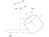
- FIG. 3 is a schematic diagram showing an example of a kneading process of an active metal paste according to an embodiment.
- 5 is a kneading vessel that contains a mixture of a binder and metal powder.
- the kneading vessel 5 rotates around an axis AX1.
- the kneading vessel 5 also revolves around an axis AX2.
- the axis AX1 is inclined with respect to the axis AX2.
- the axis AX1 is inclined with respect to the vertical direction.
- the axis AX2 is parallel to the vertical direction.
- the angle ⁇ between the axis AX1 and the axis AX2 is preferably 25 degrees or more and 50 degrees or less, and more preferably 30 degrees or more and 45 degrees or less.
- the rotation direction RD1 of the kneading vessel 5 when viewed from a direction D1 parallel to the axis AX1 is opposite to the rotation direction RD2 of the kneading vessel 5 when viewed from a direction D2 parallel to the axis AX2.
- the kneading vessel 5 rotates counterclockwise (counterclockwise) when viewed from the direction D1. Additionally, when viewed from direction D2, the kneading vessel 5 revolves clockwise.
- the kneading process includes primary kneading, secondary kneading, and tertiary kneading.
- primary kneading kneading is performed essentially by revolution only.
- secondary kneading kneading is performed by revolution and rotation.
- the revolution speed in secondary kneading is smaller than the revolution speed in primary kneading.
- the rotation speed of rotation in secondary kneading is smaller than the revolution speed in secondary kneading.
- kneading is performed by revolution and rotation.
- the revolution speed in tertiary kneading is larger than the revolution speed in secondary kneading.
- the rotation speed of rotation in tertiary kneading is smaller than the revolution speed in tertiary kneading.
- the kneading container 5 may rotate on its axis, but it is preferable that the rotation speed is sufficiently smaller than the rotation speed in secondary kneading or tertiary kneading.
- the mixture In the primary kneading, the mixture is kneaded by revolution for a preset time while maintaining the rotation speed. In the secondary and tertiary kneading, the mixture is kneaded by revolution and rotation for a preset time while maintaining the rotation speed.
- the mixture In the first kneading, the mixture is degassed by essentially only revolution. Air trapped in the mixture during the manufacturing process exists as air bubbles. If the paste with air bubbles still remains is printed, defects such as voids may occur. For this reason, it is desirable to remove the air bubbles as much as possible. If stirring is continued without sufficient degassing, the air bubbles in the mixture will be finely divided. Although the mixture appears to be degassed and the air bubbles are difficult to see, this is not desirable because it is merely a dispersion of fine defects. In order to perform sufficient degassing, it is preferable that the centrifugal acceleration of the first kneading is 80% or more of the centrifugal acceleration of the third kneading.
- the centrifugal acceleration is less than 80%, the mixture may not be sufficiently degassed. It is more preferable that the centrifugal acceleration of the first kneading is 85% or more of the centrifugal acceleration of the third kneading, and most preferably 90% or more of the centrifugal acceleration of the third kneading. On the other hand, if the centrifugal acceleration of the first kneading is too large, fine defects may be dispersed and remain as described above.
- the centrifugal acceleration of the first kneading is preferably 100% or less of the centrifugal acceleration of the third kneading, and more preferably 95% or less of the centrifugal acceleration of the third kneading.
- the time for the primary kneading is 10% or more of the total kneading time. If the kneading time is less than 10%, the mixture may not be sufficiently degassed. The longer the time for the primary kneading, the better the mixture will be degassed. However, if the primary kneading time is longer than necessary, the total time for the kneading process will be longer and the temperature of the mixture will rise. As a result, the kneading process may affect physical properties such as the paste viscosity. For this reason, the time for the primary kneading is preferably 20% or less of the total kneading time, and more preferably 15% or less.
- the degassed mixture is agitated by rotation in addition to revolution.
- the large rotation of the mixture promotes agitation of the metal powders and the binder, and the metal powder is more uniformly dispersed.
- the purpose of the secondary kneading is to agitate the entire mixture. For this reason, in the secondary kneading, kneading is performed by revolution with a smaller rotation speed than the primary kneading, and rotation with a smaller rotation speed than the revolution. By making the revolution speed smaller than that of the primary kneading, the force that moves the mixture in the centrifugal direction is suppressed.
- the mixture contains metal powder and binder. If the metal powders are not sufficiently agitated and the metal powder is not sufficiently agitated, a paste in which the metal powder is uniformly dispersed in the binder cannot be obtained. For this reason, it is desirable to agitate the metal powder in the binder as much as possible. If the paste is made without sufficient stirring, the resulting paste may contain areas that are just binder and do not contain metal powder, or may contain areas where the metal components are unevenly concentrated, which is undesirable.
- the centrifugal acceleration of the secondary kneading is 50% or more of the centrifugal acceleration of the tertiary kneading. If the centrifugal acceleration is less than 50%, the metal powder may not be sufficiently mixed. It is more preferable that the centrifugal acceleration of the secondary kneading is 60% or more of the centrifugal acceleration of the tertiary kneading, and most preferably 70% or more of the centrifugal acceleration of the tertiary kneading. On the other hand, if the centrifugal acceleration of the secondary kneading is too high, as mentioned above, pasting may proceed without mixing.
- the centrifugal acceleration of the secondary kneading is 90% or less of the centrifugal acceleration of the tertiary kneading, and more preferably 80% or less of the centrifugal acceleration of the tertiary kneading.
- the secondary kneading time is preferably 10% or more of the total kneading time. If the kneading time is less than 10%, the metal powder may not be sufficiently mixed. The longer the secondary kneading time, the more the metal powder can be mixed, but if the secondary kneading time is longer than necessary, the overall kneading time will be longer and the temperature of the mixture will rise. As a result, the kneading process may affect physical properties such as the paste viscosity. For this reason, the secondary kneading time is preferably 20% or less of the total kneading time, and more preferably 15% or less.
- tertiary kneading the mixture that has been further mixed by secondary kneading is subjected to even greater revolution and rotation to achieve greater mixing.
- the mixture is mixed by applying a shear force to it through revolution at a faster speed than in secondary kneading and rotation at a slower speed than the revolution. Mixing with shear force promotes the mixture to become a paste.
- the force applied to the mixture by tertiary kneading is greater than the force applied to the mixture by primary kneading, and preferably greater than the force applied to the mixture by secondary kneading.
- the centrifugal acceleration in tertiary kneading is greater than the centrifugal acceleration in primary kneading, and preferably greater than the centrifugal acceleration in secondary kneading.
- the kneading process includes three steps: primary kneading, secondary kneading, and tertiary kneading.
- a separate kneading step may be set between the primary and secondary kneading, between the secondary and tertiary kneading, or after the tertiary kneading.
- an increase in the overall kneading time leads to an increase in the temperature of the mixture. Therefore, if a separate step is set, it is preferable that the time of that step is short.
- the above steps produce an active metal paste.
- the paste completed by kneading is printed on a ceramic substrate.
- the printing thickness of the paste is preferably 15 to 40 ⁇ m. If the printing thickness is less than 15 ⁇ m, the thickness of the active metal brazing material layer may vary, and the bonding strength may decrease. On the other hand, if the printing thickness exceeds 40 ⁇ m, the bonding strength effect does not improve, resulting in an increase in costs.
- the paste is printed in a uniform thickness on the end surface of the ceramic component by a screen printing method or the like. If the printing thickness is not uniform, the active metal brazing material will be excessive in the thick parts, causing brazing material pools and cracks due to thermal stress.
- the difference in thickness between the thickest and thinnest parts of the printed paste is preferably 10 ⁇ m or less, and more preferably 5 ⁇ m or less.
- FIG. 4(A) to FIG. 4(E) are cross-sectional views showing an example of a manufacturing process of a ceramic circuit board according to an embodiment.
- FIG. 4(A) shows a ceramic substrate 2 before printing an active metal paste 6.
- the active metal paste 6 is printed on the upper surface of the ceramic substrate 2 and dried. In the illustrated example, the active metal paste 6 is selectively printed only in the area where the metal circuit will be provided thereafter.
- the active metal paste 6 is printed on the lower surface of the ceramic substrate 2 and dried.
- a metal plate 7 is placed on the surface of the dried active metal paste 6 and bonded. The active metal paste 6 melts and solidifies to form a bonding layer 4.
- the metal plate 7 is processed into the shape of the metal circuit by etching or the like to form the metal circuit 3.
- a ceramic circuit substrate 1 including a ceramic substrate 2 and a metal circuit 3 is manufactured.
- active metal paste 6 may be printed on the upper surface of ceramic substrate 2 over an area larger than metal circuit 3. In this case, after part of metal plate 7 is etched, part of bonding layer 4 is etched. It is also possible to prepare pre-processed metal circuits 3 and place these metal circuits 3 on top of active metal paste 6. In this case, the etching process shown in FIG. 4(D) is omitted.
- a thin metal film may be provided on the surface of the metal circuit 3 of the ceramic circuit board 1.
- the thin metal film has as its main component one selected from the group consisting of Ni (nickel), Ag (silver), and Au (gold).
- main component refers to a component that is present at 50% or more.
- the thin metal film may be a plated film, a sputtered film, etc.
- FIGS. 5(A) and 5(B) are side views showing an example of a semiconductor device according to an embodiment.
- the ceramic circuit board 1 according to the embodiment is suitable for a semiconductor device.
- a semiconductor element is mounted on a metal circuit 3 via a bonding layer.
- 1 is a ceramic circuit board.
- 8 is a bonding layer.
- 9 is a semiconductor element.
- 10 is a semiconductor device.
- 11 is wire bonding.
- 12 is a lead frame.
- 13 is a molded resin.
- FIG. 5(B) shows the semiconductor device 10 shown in FIG. 5(A) covered with molded resin 13.
- a semiconductor element 9 is mounted on the metal circuit 3 of the ceramic circuit board 1 via a bonding layer 8. Adjacent metal circuits 3 are electrically connected to each other by wire bonding 11.
- the semiconductor device 10 according to the embodiment is not limited to such a structure.
- a plurality of semiconductor elements 9 and wire bonding 11 may be provided on the metal circuit 3 on the upper surface.
- a semiconductor element, wire bonding, etc. may be bonded to the metal circuit 3 on the lower surface as necessary.
- Metal terminals such as a lead frame may be bonded to the ceramic circuit board 1. Solder, brazing material, etc. are used for the bonding layer 8 that bonds the semiconductor element 9.
- the solder is preferably a lead-free solder.
- solder refers to a bonding material with a melting point of 450°C or less.
- Brazing material refers to a bonding material with a melting point of more than 450°C.
- a bonding material with a melting point of 500°C or more is called a high-temperature brazing material.
- An example of a high-temperature brazing material is a material mainly composed of Ag.
- the ceramic circuit board 1 on which the semiconductor element 9 is mounted is required to have improved heat dissipation.
- multiple semiconductor elements 9 can be mounted on the ceramic circuit board 1. If any of the semiconductor elements 9 exceeds the intrinsic temperature of the element, the resistance changes to a negative temperature coefficient. As a result, thermal runaway occurs in which power flows intensively, and the semiconductor device 10 is instantly destroyed. Therefore, it is very effective to improve the reliability of the connection between the semiconductor element 9 and the metal circuit 3.
- the semiconductor device 10 according to the embodiment can be used in PCU, IGBT, and IPM modules.
- PCU, IGBT, and IPM modules are used in inverters for automobiles (including electric vehicles), electric railway vehicles, industrial machinery, and air conditioners.
- automobiles electric vehicles are becoming more and more popular. The more the reliability of the semiconductor device improves, the more the safety of the automobile can be improved. The same is true for electric railway vehicles, industrial equipment, and the like.
- a specific example of a method for manufacturing the ceramic circuit board 1 according to the embodiment will be described. As long as the ceramic circuit board 1 has the above-mentioned configuration, the manufacturing method is not particularly limited. Here, an example of a method for obtaining the ceramic circuit board 1 with a good yield will be given.
- the ceramic substrate 2 and the metal plate 7 are prepared.
- the ceramic substrate 2 is preferably one selected from a silicon nitride substrate, an aluminum nitride substrate, and an aluminum oxide substrate.
- the ceramic substrate 2 is preferably a silicon nitride substrate having a thermal conductivity of 50 W/(m ⁇ K) or more and a three-point bending strength of 600 MPa or more.
- the metal plate 7 is preferably made of one selected from copper or a copper alloy.
- the through holes may be provided in advance at the stage of the molded body.
- the through holes may also be provided in the ceramic substrate 2 (ceramic sintered body).
- the through holes are provided by laser processing, cutting processing, etc. Examples of cutting processing include drilling using a drill or the like.
- the ceramic substrate 2 is preferably joined to a copper plate or a copper alloy plate by an active metal joining method.
- an active metal brazing material in which an active metal such as Ti is mixed with Cu is used.
- active metal brazing materials include a mixture of Ti and Cu, and a mixture of Ti, Ag, and Cu.
- the Cu content in the inorganic components contained in the mixture is 50 mass% or more
- the Ti content is 4 mass% to 30 mass%
- the content of one or two selected from Sn and In is 5 mass% to 45 mass%
- the C content is 0 mass% to 2 mass%.
- “Inorganic components” are components other than organic components contained in organic solvents, resins, etc., and refer to metal elements such as Ag, Cu, and active metals contained in metal powder, and inorganic components other than metals such as Si and C.
- the Ag content in the inorganic components contained in the mixture is 20% by mass to 60% by mass
- the Cu content is 15% by mass to 40% by mass
- the Ti content is 1% by mass to 15% by mass
- the content of one or two selected from Sn and In is 5% by mass to 25% by mass.
- one or more selected from the group consisting of Al, Si, and Mg may be added in the range of 1 to 15% by mass.
- the active metal brazing material is made into a paste.
- the binder to be mixed with the metal powder is prepared.
- the binder is prepared by dissolving the resin component in an organic solvent.
- a preferred example of the resin used in the binder preparation is ethyl cellulose.
- a preferred example of the organic solvent is terpineol. If the binder contains a lot of resin and little organic solvent, the binder will have a high viscosity, making it difficult for the binder to mix with the metal powder. If the binder contains little resin and much organic solvent, the binder will have a low viscosity, and a paste suitable for printing will not be obtained. For this reason, the amount of resin contained in the binder is preferably 5 to 15% by mass.
- dispersants and surfactants such as sodium lauroyl sarcosine and oleic acid may be added as necessary to help dispersion and prevent aggregation.
- the amount of dispersant or surfactant added is 0.1 to 5% by mass. If the resin is not easily soluble in the organic solvent, stirring is performed using a stirrer or mixer, or stirring is performed by rotating the binder in an airtight container using a pot roller or the like to ensure that no resin components remain dissolved in the organic solvent.
- premixing the binder prepared in the binder preparation is mixed with the metal components.
- the binder and metal powder are mixed and blended using a stirrer or crusher.
- Metal powder may remain unmixed, so mixing is performed so that no lumps of metal powder are visible to the naked eye. Since premixing does not involve sufficient mixing or stirring, there is a possibility that the binder and metal components will separate if left unattended. For this reason, kneading is performed promptly after premixing.
- the mixture of premixed binder and metal powder is turned into a paste.
- the premixed mixture is placed in a kneading container with an airtight lid made of polyethylene or polypropylene.
- the mixture in the kneading container is kneaded by rotating it using a self-rotating device.
- self-rotating devices include the SK series from Shashin Kagaku and the ARE series from Thinky.
- the mixture is degassed and agitation is promoted to form a paste. It is preferable to set rotation and revolution conditions suitable for degassing, agitation, and pasting, and to knead efficiently by dividing the steps into primary kneading, secondary kneading, and tertiary kneading.
- the centrifugal acceleration of the primary kneading is preferably 80% or more of the centrifugal acceleration of the tertiary kneading required for forming a paste.
- the time of the primary kneading is preferably 10% or more of the total kneading time.
- the centrifugal acceleration is preferably 80G or more and the kneading time is preferably 45 seconds or more.
- the secondary kneading is carried out immediately after the primary kneading.
- rotation is performed in addition to revolution. This promotes the agitation of the degassed mixture by the rotation.
- the kneading is carried out by revolution with a lower rotation speed than the primary kneading and rotation with a lower rotation speed than the revolution.
- the centrifugal acceleration of the secondary kneading is preferably 50% or more of the centrifugal acceleration of the tertiary kneading.
- the time of the secondary kneading is preferably 10% or more of the total kneading time.
- the centrifugal acceleration is preferably 65G or more and the kneading time is preferably 45 seconds or more.
- the tertiary kneading is carried out immediately after the secondary kneading.
- the mixture that has been further stirred by the secondary kneading is subjected to even greater revolution and rotation to stir the mixture.
- revolution By performing revolution at a higher rotation speed than in the secondary kneading and rotation at a lower rotation speed than the revolution, the mixture is stirred with shear force applied. This stirring with shear force promotes the mixture to become a paste.
- the force applied to the mixture by the tertiary kneading is preferably greater than that of the primary kneading and secondary kneading.
- the centrifugal acceleration in the tertiary kneading is preferably greater than that of the primary kneading and secondary kneading.
- the centrifugal acceleration is preferably 100 G or more and the kneading time is preferably 250 seconds or more.
- the active metal paste completed by kneading is printed onto the ceramic substrate.
- the active metal paste is printed in a uniform thickness using a method such as screen printing.
- the printing thickness of the paste is preferably 15 to 40 ⁇ m.
- the active metal paste is printed on one side and then dried by heating in the air. The active metal paste is then printed on the other side and the paste is dried in the same manner.
- a metal plate is placed on the ceramic substrate on which the active metal paste has been printed and dried.
- the ceramic substrate on which the metal plate has been placed is heated at 700 to 900° C. to bond the ceramic substrate and the metal plate.
- the heating step is carried out in a vacuum or a non-oxidizing atmosphere as necessary.
- the pressure is preferably 1 ⁇ 10 ⁇ 2 Pa or less.
- the non-oxidizing atmosphere include a nitrogen atmosphere and an argon atmosphere.
- the active metal paste melts and solidifies by the heat bonding.
- the active metal paste functions as a bonding layer that bonds the ceramic substrate and the metal plate.
- a ceramic circuit board can be obtained by bonding the machined metal circuit to a ceramic substrate. If a metal plate that has not been machined into a circuit shape is bonded to a ceramic substrate, the metal circuit is formed by etching or other methods. Not only the metal plate, but also the bonding layer can be machined into a circuit shape by etching.
- the above-mentioned steps allow the manufacture of a ceramic circuit board.
- a step of bonding a semiconductor element or the like to the ceramic circuit board is performed.
- a bonding layer is provided at the location where the semiconductor element is to be bonded.
- the bonding layer preferably contains solder or brazing material.
- the semiconductor element is provided on the bonding layer. Wire bonding may be provided as necessary. Multiple semiconductor elements and multiple wire bonding may be provided as necessary.
- an active metal paste is obtained in which the components are more uniformly dispersed and with fewer air bubbles.
- active metals are chemically active and highly reactive. For this reason, it is desirable to disperse them uniformly in the paste efficiently and in a shorter time.
- the kneading process allows each component of the metal powder, including the active metal, to be dispersed more uniformly in the paste in a shorter time.
- an active metal paste in which the dispersibility of the copper element and the active metal element are each less than 1.0.
- the dispersibility of the copper element and the active metal element being less than 1.0 means that the copper element and the active metal element are sufficiently dispersed in the active metal paste.
- the dispersibility of the copper element and the active metal element being less than 1.0 suppresses aggregation and improves the fluidity of the paste. This makes it easier to print the active metal paste. In addition, each particle easily enters between other particles, so the reaction proceeds efficiently and bonding is improved.
- the ceramic substrates shown in Table 1 were prepared.
- the ceramic substrates were silicon nitride substrates or aluminum nitride substrates.
- the thermal conductivity of the silicon nitride substrate was 90 W/(m ⁇ K) and the three-point bending strength was 650 MPa.
- the thermal conductivity of the aluminum nitride substrate was 170 W/(m ⁇ K) and the three-point bending strength was 300 MPa.
- the size of the ceramic substrate was 30 mm long x 50 mm wide.
- the thickness of the silicon nitride substrate was 0.32 mm, and the thickness of the aluminum nitride substrate was 0.635 mm.
- the silicon nitride substrate is represented as Si 3 N 4
- the aluminum nitride substrate is represented as AlN.
- metal powders were prepared, which are the metal components of the paste shown in Table 1.
- the metal powders were silver-based powder (Ag-Cu-Sn-Ti) or copper-based powder (Cu-Sn-TiH).
- the ratios of each metal component in the silver-based powder were 58 mass% Ag, 30 mass% Cu, 10 mass% Sn, and 2 mass% Ti.
- the ratios of each metal component in the copper-based powder were 68 mass% Cu, 20 mass% Sn, and 12 mass% TiH.
- the average particle size of the Ag powder was 2 ⁇ m.
- the average particle size of the Cu powder was 1 ⁇ m.
- the average particle size of the Sn powder was 5 ⁇ m.
- the average particle size of the Ti powder was 5 ⁇ m.
- the average particle size of the TiH powder was 6 ⁇ m.
- the binder was prepared. 7% by mass of ethyl cellulose, 3% by mass of sarcosinate, and 90% by mass of terpineol were placed in a wide-mouth polyethylene bottle with a lid, and the bottle was rotated on a pot roller for 24 hours to prepare the binder.
- premixing was performed to mix the metal powder and binder. 20% by mass of binder was placed in a polyethylene cylindrical container, with the total metal powder being 100% by mass. The stirring blade was fixed vertically to the opening of the cylindrical container, and the cylindrical container was rotated at 50 rpm for 3 minutes to perform premixing and produce a mixture of metal powder and binder.
- the premixed mixture of binder and metal powder is kneaded to make a paste.
- a sealed lid is attached to the cylindrical polyethylene container containing the premixed mixture, and the first, second, and third kneading are carried out using a kneading device.
- the kneading device used is the SK-3000 made by Photo Chemical.
- the kneading conditions for each step, including the rotation speed (rpm), revolution speed (rpm), centrifugal acceleration (G), and kneading time (seconds), are shown in Tables 1 and 2.
- Table 2 lists the ratio (G2/G3) of the centrifugal acceleration of the secondary kneading (G2) to the centrifugal acceleration of the tertiary kneading (G3), and the ratio (T2/T1-3) of the secondary kneading time (T2) to the total kneading time (T1-3).
- the ratio of the centrifugal acceleration of the primary kneading to the centrifugal acceleration of the tertiary kneading (G1/G3) and the ratio of the primary kneading time to the total kneading time (T1/T1-3) were within the preferred ranges.
- the ratio of the centrifugal acceleration of the secondary kneading to the centrifugal acceleration of the tertiary kneading (G2/G3) and the ratio of the secondary kneading time to the total kneading time (T2/T1-3) were within the preferred ranges.
- these values were outside the preferred ranges.
- the maximum agglomerated particle size was measured using a grind gauge.
- the grind gauge is a metal block gauge with a groove with a sloping bottom carved into its surface. One end of the groove is zero depth.
- the maximum agglomerated particle size can be easily measured by putting paste into the deep side of the groove and pulling the paste from the deep side to the shallow side with a metal squeegee.
- Pastes with a maximum agglomerated particle size of less than 10 ⁇ m were determined to be pastes without large agglomerations.
- Table 3 examples where the measured maximum agglomerated particle size was less than 10 ⁇ m are marked as "OK", and examples where the measured maximum agglomerated particle size was 10 ⁇ m or more are marked as "NG”.
- the active metal paste completed by kneading was printed on a ceramic substrate.
- the active metal paste was printed using a screen plate measuring 320 mm x 320 mm and with a mesh size of 200 ⁇ m.
- three rectangular circuit shapes were printed on one side (top) of the ceramic substrate.
- the active metal paste printed on one side was dried by heating in air at 100°C for one minute.
- one rectangular circuit shape was printed on the other side (bottom).
- the active metal paste printed on the other side was dried by heating in air at 100°C for one minute.
- the dispersibility of Cu particles and the dispersibility of active metal particles were evaluated to confirm the dispersion of the metal powder in the paste after printing and drying.
- the paste is printed and dried on a polyethylene terephthalate (PET) film under the same conditions as the ceramic substrate.
- PET polyethylene terephthalate
- the flat surface of the paste on the film side is observed with an energy dispersive X-ray analyzer (SEM-EDX).
- SEM-EDX energy dispersive X-ray analyzer
- the size of the observation area is set to 100 ⁇ m x 80 ⁇ m. Mapping data of the Cu element and mapping data of the active metal element present in the observation area are obtained. From the mapping data of the Cu element, the particle size distribution is calculated using particle size analysis software.
- the mapping data of the Cu element is divided by Voronoi division.
- the divided area distribution is measured, and the average area and standard deviation are calculated.
- the standard deviation is divided by the average value to calculate the value as the dispersibility (standard deviation/average value).
- the particle size distribution is calculated from the mapping data of the active metal elements using particle size analysis software.
- the divided area distribution is measured, and the average area and standard deviation are calculated.
- the standard deviation is divided by the average value to calculate the dispersibility (standard deviation/average value).
- ImageJ can be used as the particle size analysis software.
- oxygen-free copper plates measuring 30 mm length x 50 mm width x 0.8 mm thickness were placed on both sides of the ceramic substrate on which the paste had been printed and dried, and thermal bonding was performed.
- silver-based paste Ag-Cu-Sn-Ti
- Cu-Sn-TiH copper-based paste
- the bonding time for each was set to 10 minutes, and bonding was performed in a vacuum (1 ⁇ 10 ⁇ 2 Pa or less).
- the oxygen-free copper plate to which the ceramic substrate was bonded was etched.
- metal circuits were formed in three places on the front surface of the ceramic substrate, and one metal circuit was formed in one place on the rear surface.
- a pullback of 5 mm was formed from the periphery of the ceramic substrate, and a non-circuit section of 5 mm was also formed between the circuit shapes.
- a pullback of 5 mm was formed from the periphery of the ceramic substrate.
- voids in the bonding layer of the surface circuit were measured using ultrasonic flaw detection (SAT: Scanning Acoustic Tomograph). Any defects with a diameter of 1 mm or more were judged to be void defects. In Table 3, those that were not judged to be void defects are marked as "OK” and those that were judged to be void defects are marked as "NG.”
- the peel strength was measured as the bonding strength between the metal circuit and the ceramic substrate.
- the peel strength was measured by fixing the ceramic circuit substrate to a jig and peeling off part of the upper surface metal circuit vertically at 50 mm/min. The respective measurement results are shown in Table 3.
- the pastes of Examples 1 to 12 did not show poor cohesion, and the dispersibility values were within the preferred range. This is thought to be because the paste mixing conditions were set within the preferred range, which prevented the occurrence of air bubbles and agglomerations in the paste. In contrast, in Comparative Examples 1 to 10, there were cases where poor cohesion was observed, and the dispersibility values were outside the preferred range. This is thought to be because air bubbles and agglomerations were not eliminated and remained in the paste.
- the ceramic circuit board according to the embodiment has few bonding defects and high bonding strength, making it ideal for semiconductor devices equipped with semiconductor elements.
- Embodiments of the invention include the following features.
- Feature 1 a pre-mixing step of mixing a metal powder containing copper and an active metal with a binder having a resin dissolved in an organic solvent to produce a mixture containing 60 to 95 mass % of the metal powder; and a kneading step of subjecting the mixture to rotation and revolution to produce an active metal paste.
- the kneading step includes a primary kneading step of kneading by revolution, a secondary kneading step of kneading by revolution and rotation after the primary kneading, and a tertiary kneading step of kneading by revolution and rotation after the secondary kneading,
- the rotation speed of the revolution in the secondary kneading is smaller than the rotation speed of the revolution in the primary kneading
- the rotation speed of the rotation in the secondary kneading is smaller than the rotation speed of the revolution in the secondary kneading
- the rotation speed of the revolution in the tertiary kneading is greater than the rotation speed of the revolution in the secondary kneading, 2.
- (Feature 3) 3.
- a centrifugal acceleration of the first kneading is 80% or more of a centrifugal acceleration of the third kneading
- a centrifugal acceleration of the second kneading is 50% or more of a centrifugal acceleration of the third kneading.
- a time for the first kneading and a time for the second kneading are each 10% or more of a total kneading time.
- (Feature 5) A step of carrying out a method for producing an active metal paste according to any one of features 1 to 4; a bonding step of bonding a metal member to a ceramic substrate via the active metal paste;
- a method for manufacturing a ceramic circuit board comprising the steps of: (Feature 6) A step of carrying out a method for producing an active metal paste according to any one of features 1 to 4; a bonding step of bonding a metal member to a ceramic substrate via the active metal paste; a mounting step of mounting a semiconductor element on the metal member on which a circuit is formed;
- a method for manufacturing a semiconductor device comprising the steps of: (Feature 7)
- An active metal paste comprising copper and at least one active metal, the active metal paste being characterized in that the dispersibility of the copper element and the active metal element are each less than 1.0.
- (Feature 8) The active metal paste according to Feature 7, wherein, among the inorganic components, the copper content is 50% by mass or more, the active metal content is 4% by mass or more and 30% by mass or less, the content of one or two selected from tin and indium is 5% by mass or more and 45% by mass or less, and the carbon content is 0% by mass or more and 2% by mass or less. (Feature 9) 8.
Landscapes
- Engineering & Computer Science (AREA)
- Mechanical Engineering (AREA)
- Chemical & Material Sciences (AREA)
- Materials Engineering (AREA)
- Metallurgy (AREA)
- Organic Chemistry (AREA)
- Composite Materials (AREA)
- Manufacturing & Machinery (AREA)
- Microelectronics & Electronic Packaging (AREA)
- Chemical Kinetics & Catalysis (AREA)
- Manufacturing Of Printed Wiring (AREA)
- Conductive Materials (AREA)
- Ceramic Engineering (AREA)
Priority Applications (4)
| Application Number | Priority Date | Filing Date | Title |
|---|---|---|---|
| CN202380038547.8A CN119173349A (zh) | 2023-01-17 | 2023-12-13 | 活性金属糊剂的制造方法、陶瓷电路基板的制造方法、半导体装置的制造方法、活性金属糊剂、陶瓷电路基板及半导体装置 |
| EP23917703.3A EP4653111A1 (en) | 2023-01-17 | 2023-12-13 | Method for producing active metal paste, method for producing ceramic circuit board, method for producing semiconductor device, active metal paste, ceramic circuit board, and semiconductor device |
| JP2024547940A JPWO2024154492A1 (cg-RX-API-DMAC7.html) | 2023-01-17 | 2023-12-13 | |
| US18/953,179 US20250073826A1 (en) | 2023-01-17 | 2024-11-20 | Method for producing active metal paste, method for producing ceramic circuit board, method for producing semiconductor device, active metal paste, ceramic circuit board, and semiconductor device |
Applications Claiming Priority (2)
| Application Number | Priority Date | Filing Date | Title |
|---|---|---|---|
| JP2023004797 | 2023-01-17 | ||
| JP2023-004797 | 2023-01-17 |
Related Child Applications (1)
| Application Number | Title | Priority Date | Filing Date |
|---|---|---|---|
| US18/953,179 Continuation US20250073826A1 (en) | 2023-01-17 | 2024-11-20 | Method for producing active metal paste, method for producing ceramic circuit board, method for producing semiconductor device, active metal paste, ceramic circuit board, and semiconductor device |
Publications (1)
| Publication Number | Publication Date |
|---|---|
| WO2024154492A1 true WO2024154492A1 (ja) | 2024-07-25 |
Family
ID=91955801
Family Applications (1)
| Application Number | Title | Priority Date | Filing Date |
|---|---|---|---|
| PCT/JP2023/044719 Ceased WO2024154492A1 (ja) | 2023-01-17 | 2023-12-13 | 活性金属ペーストの製造方法、セラミックス回路基板の製造方法、半導体装置の製造方法、活性金属ペースト、セラミックス回路基板、及び半導体装置 |
Country Status (5)
| Country | Link |
|---|---|
| US (1) | US20250073826A1 (cg-RX-API-DMAC7.html) |
| EP (1) | EP4653111A1 (cg-RX-API-DMAC7.html) |
| JP (1) | JPWO2024154492A1 (cg-RX-API-DMAC7.html) |
| CN (1) | CN119173349A (cg-RX-API-DMAC7.html) |
| WO (1) | WO2024154492A1 (cg-RX-API-DMAC7.html) |
Cited By (1)
| Publication number | Priority date | Publication date | Assignee | Title |
|---|---|---|---|---|
| WO2026014525A1 (ja) * | 2024-07-12 | 2026-01-15 | 福田金属箔粉工業株式会社 | ろう粉末およびそれを含むペースト組成物 |
Citations (5)
| Publication number | Priority date | Publication date | Assignee | Title |
|---|---|---|---|---|
| JP2004314161A (ja) * | 2003-04-21 | 2004-11-11 | Hitachi Metals Ltd | セラミックス基板用ろう材及びこれを用いたセラミックス回路基板 |
| JP5790433B2 (ja) | 2011-11-18 | 2015-10-07 | 住友金属鉱山株式会社 | 銀粉及びその製造方法 |
| WO2017056360A1 (ja) * | 2015-09-28 | 2017-04-06 | 株式会社 東芝 | 回路基板および半導体装置 |
| WO2020138283A1 (ja) * | 2018-12-28 | 2020-07-02 | デンカ株式会社 | セラミックス-銅複合体、セラミックス回路基板、パワーモジュール及びセラミックス-銅複合体の製造方法 |
| WO2021235387A1 (ja) * | 2020-05-20 | 2021-11-25 | 株式会社 東芝 | 接合体、セラミックス銅回路基板、及び半導体装置 |
Family Cites Families (2)
| Publication number | Priority date | Publication date | Assignee | Title |
|---|---|---|---|---|
| WO2012070262A1 (ja) | 2010-11-22 | 2012-05-31 | Dowaエレクトロニクス株式会社 | 接合材料および接合体、並びに接合方法 |
| EP4234517B1 (en) | 2020-10-20 | 2025-10-01 | Kabushiki Kaisha Toshiba | Bonded body, ceramic circuit board using same, and semiconductor device |
-
2023
- 2023-12-13 WO PCT/JP2023/044719 patent/WO2024154492A1/ja not_active Ceased
- 2023-12-13 CN CN202380038547.8A patent/CN119173349A/zh active Pending
- 2023-12-13 JP JP2024547940A patent/JPWO2024154492A1/ja active Pending
- 2023-12-13 EP EP23917703.3A patent/EP4653111A1/en active Pending
-
2024
- 2024-11-20 US US18/953,179 patent/US20250073826A1/en active Pending
Patent Citations (5)
| Publication number | Priority date | Publication date | Assignee | Title |
|---|---|---|---|---|
| JP2004314161A (ja) * | 2003-04-21 | 2004-11-11 | Hitachi Metals Ltd | セラミックス基板用ろう材及びこれを用いたセラミックス回路基板 |
| JP5790433B2 (ja) | 2011-11-18 | 2015-10-07 | 住友金属鉱山株式会社 | 銀粉及びその製造方法 |
| WO2017056360A1 (ja) * | 2015-09-28 | 2017-04-06 | 株式会社 東芝 | 回路基板および半導体装置 |
| WO2020138283A1 (ja) * | 2018-12-28 | 2020-07-02 | デンカ株式会社 | セラミックス-銅複合体、セラミックス回路基板、パワーモジュール及びセラミックス-銅複合体の製造方法 |
| WO2021235387A1 (ja) * | 2020-05-20 | 2021-11-25 | 株式会社 東芝 | 接合体、セラミックス銅回路基板、及び半導体装置 |
Non-Patent Citations (1)
| Title |
|---|
| See also references of EP4653111A1 |
Cited By (1)
| Publication number | Priority date | Publication date | Assignee | Title |
|---|---|---|---|---|
| WO2026014525A1 (ja) * | 2024-07-12 | 2026-01-15 | 福田金属箔粉工業株式会社 | ろう粉末およびそれを含むペースト組成物 |
Also Published As
| Publication number | Publication date |
|---|---|
| US20250073826A1 (en) | 2025-03-06 |
| EP4653111A1 (en) | 2025-11-26 |
| JPWO2024154492A1 (cg-RX-API-DMAC7.html) | 2024-07-25 |
| CN119173349A (zh) | 2024-12-20 |
Similar Documents
| Publication | Publication Date | Title |
|---|---|---|
| KR102078891B1 (ko) | 파워 모듈용 기판, 히트 싱크가 부착된 파워 모듈용 기판, 파워 모듈, 파워 모듈용 기판의 제조 방법, 및 동 부재 접합용 페이스트 | |
| CN1254160C (zh) | 陶瓷电子部件及其制造方法 | |
| JP7110410B2 (ja) | 焼結ダイアタッチ及び類似した用途のためのナノ銅ペースト及びフィルム | |
| JP7210842B2 (ja) | 接合体の製造方法、焼結銅ピラー形成用銅ペースト、及び接合用ピラー付部材 | |
| EP3778069A1 (en) | Copper paste, bonding method, and method for producing bonded body | |
| JP6056432B2 (ja) | パワーモジュール用基板、ヒートシンク付パワーモジュール用基板、パワーモジュール、パワーモジュール用基板の製造方法 | |
| KR20180004853A (ko) | 접합재료, 접합체, 및 접합방법 | |
| WO2013122126A1 (ja) | はんだ接合構造、パワーモジュール、ヒートシンク付パワーモジュール用基板及びそれらの製造方法、並びにはんだ下地層形成用ペースト | |
| WO2017138252A1 (ja) | 導電性接着フィルムおよびこれを用いたダイシング・ダイボンディングフィルム | |
| KR20170020861A (ko) | 다층 금속 나노 및 미크론 입자 | |
| CN115894064B (zh) | 一种低银含陶瓷金属化用amb浆料及其制备方法 | |
| JP5844299B2 (ja) | 接合材、接合構造体 | |
| JP2018152176A (ja) | 接合用銅ペースト及び半導体装置 | |
| JP2013041884A (ja) | 半導体装置 | |
| US20250073826A1 (en) | Method for producing active metal paste, method for producing ceramic circuit board, method for producing semiconductor device, active metal paste, ceramic circuit board, and semiconductor device | |
| CN118956290A (zh) | 一种低温无压烧结银胶 | |
| WO2020004342A1 (ja) | 銀ペースト及び接合体の製造方法 | |
| CN114173983A (zh) | 预制焊料和使用该预制焊料形成的焊料接合体 | |
| CN111033703A (zh) | 安装结构体以及纳米粒子安装材料 | |
| JP7500943B2 (ja) | 接合用金属ペースト、接合体の製造方法、及び接合体 | |
| US20260042174A1 (en) | Joining material and method of producing joined body | |
| WO2026023666A1 (ja) | セラミックス銅回路基板、半導体装置、およびセラミックス銅回路基板の製造方法 | |
| JP2025168438A (ja) | スクレイパー及びそれを用いたスクリーン印刷機、ならびに該スクレイパーを用いたセラミックス回路基板及び半導体装置の製造方法 | |
| JP2012174366A (ja) | はんだ下地層形成用ペースト |
Legal Events
| Date | Code | Title | Description |
|---|---|---|---|
| WWE | Wipo information: entry into national phase |
Ref document number: 2024547940 Country of ref document: JP |
|
| 121 | Ep: the epo has been informed by wipo that ep was designated in this application |
Ref document number: 23917703 Country of ref document: EP Kind code of ref document: A1 |
|
| NENP | Non-entry into the national phase |
Ref country code: DE |
|
| WWP | Wipo information: published in national office |
Ref document number: 2023917703 Country of ref document: EP |