WO2024154308A1 - モジュラー・マルチレベル電力変換器 - Google Patents
モジュラー・マルチレベル電力変換器 Download PDFInfo
- Publication number
- WO2024154308A1 WO2024154308A1 PCT/JP2023/001587 JP2023001587W WO2024154308A1 WO 2024154308 A1 WO2024154308 A1 WO 2024154308A1 JP 2023001587 W JP2023001587 W JP 2023001587W WO 2024154308 A1 WO2024154308 A1 WO 2024154308A1
- Authority
- WO
- WIPO (PCT)
- Prior art keywords
- arm
- positive
- control device
- negative
- current
- Prior art date
- Legal status (The legal status is an assumption and is not a legal conclusion. Google has not performed a legal analysis and makes no representation as to the accuracy of the status listed.)
- Ceased
Links
Images













Classifications
-
- H—ELECTRICITY
- H02—GENERATION; CONVERSION OR DISTRIBUTION OF ELECTRIC POWER
- H02M—APPARATUS FOR CONVERSION BETWEEN AC AND AC, BETWEEN AC AND DC, OR BETWEEN DC AND DC, AND FOR USE WITH MAINS OR SIMILAR POWER SUPPLY SYSTEMS; CONVERSION OF DC OR AC INPUT POWER INTO SURGE OUTPUT POWER; CONTROL OR REGULATION THEREOF
- H02M7/00—Conversion of AC power input into DC power output; Conversion of DC power input into AC power output
- H02M7/42—Conversion of DC power input into AC power output without possibility of reversal
- H02M7/44—Conversion of DC power input into AC power output without possibility of reversal by static converters
- H02M7/48—Conversion of DC power input into AC power output without possibility of reversal by static converters using discharge tubes with control electrode or semiconductor devices with control electrode
- H02M7/483—Converters with outputs that each can have more than two voltages levels
- H02M7/4835—Converters with outputs that each can have more than two voltages levels comprising two or more cells, each including a switchable capacitor, the capacitors having a nominal charge voltage which corresponds to a given fraction of the input voltage, and the capacitors being selectively connected in series to determine the instantaneous output voltage
-
- H—ELECTRICITY
- H02—GENERATION; CONVERSION OR DISTRIBUTION OF ELECTRIC POWER
- H02M—APPARATUS FOR CONVERSION BETWEEN AC AND AC, BETWEEN AC AND DC, OR BETWEEN DC AND DC, AND FOR USE WITH MAINS OR SIMILAR POWER SUPPLY SYSTEMS; CONVERSION OF DC OR AC INPUT POWER INTO SURGE OUTPUT POWER; CONTROL OR REGULATION THEREOF
- H02M1/00—Details of apparatus for conversion
- H02M1/0003—Details of control, feedback or regulation circuits
-
- H—ELECTRICITY
- H02—GENERATION; CONVERSION OR DISTRIBUTION OF ELECTRIC POWER
- H02M—APPARATUS FOR CONVERSION BETWEEN AC AND AC, BETWEEN AC AND DC, OR BETWEEN DC AND DC, AND FOR USE WITH MAINS OR SIMILAR POWER SUPPLY SYSTEMS; CONVERSION OF DC OR AC INPUT POWER INTO SURGE OUTPUT POWER; CONTROL OR REGULATION THEREOF
- H02M7/00—Conversion of AC power input into DC power output; Conversion of DC power input into AC power output
- H02M7/42—Conversion of DC power input into AC power output without possibility of reversal
- H02M7/44—Conversion of DC power input into AC power output without possibility of reversal by static converters
- H02M7/48—Conversion of DC power input into AC power output without possibility of reversal by static converters using discharge tubes with control electrode or semiconductor devices with control electrode
- H02M7/483—Converters with outputs that each can have more than two voltages levels
- H02M7/4833—Capacitor voltage balancing
Definitions
- the present invention relates to a modular multilevel power converter (hereinafter, in this invention, referred to as an "MMC converter").
- MMC converter modular multilevel power converter
- the present invention relates to a modular multilevel power converter suitable for forming a frequency conversion device by connecting the DC sides of two MMC converters back to back.
- the MMC converter circuit consists of a unit converter that generates the required voltage by controlling the modulation rate of a PWM converter that uses an energy storage element with voltage source characteristics, such as a capacitor, as a voltage source.
- the capacitor voltage of the unit converter fluctuates due to charging and discharging in a period determined by the AC frequency.
- Six two-terminal arms are provided with K unit converters connected in series, three of which are used as positive arms with their negative terminals connected to each phase terminal of the AC power supply and their star-connected positive terminals connected to the positive terminal of the DC power supply. The remaining three are used as negative arms with their positive terminals connected to each phase terminal of the AC power supply and their star-connected negative terminals connected to the negative terminal of the DC power supply.
- the characteristic of the MMC converter is that it requires capacitor voltage control to keep the voltages of the 6 x K capacitors in the unit converter within a specified range.
- the functions required for capacitor voltage control can be divided into three functions: a function for balancing K capacitor voltages by mutually adjusting the modulation rates of K PWM converters provided for each unit converter within the same arm (hereinafter referred to as "intra-arm balance control” in this invention); a function for balancing the average voltages of the 2 x K capacitors that make up the positive arm and negative arm of each phase between each phase (hereinafter referred to as “inter-leg balance control” in this invention); and a function for balancing the difference voltage between the average voltages of the K capacitors in the positive arm and the average voltages of the K capacitors in the negative arm (hereinafter referred to as "positive-negative balance control” in this invention).
- Patent Document 1 discloses a basic circuit configuration in which an inductive element such as a reactor is provided between the first terminal of the positive arm and the AC terminal, and between the second terminal of the negative arm and the AC terminal, in order to suppress through current from the negative arm to the positive arm of the MMC converter.
- an inductive element such as a reactor
- Patent Document 2 discloses a basic circuit configuration in which the windings of the positive arm and the negative arm of each phase are magnetically coupled by the first to third iron core legs to suppress through current from the negative arm to the positive arm of the MMC converter, and a three-phase five-leg reactor is provided in which the through current of each phase is magnetically coupled by the fourth and fifth iron core legs to reduce the size.
- Patent document 3 discloses the basic hierarchical structure of a control system consisting of a PWM modulator and converter current control provided for each unit converter of an MMC converter. It also discloses a method of adding a second harmonic circulating current command to a fundamental current command.
- Patent document 4 discloses a method for realizing a variable speed generator/motor by connecting the AC side of one of two MMC converters, the DC side of which is connected back-to-back, to an AC rotating electric machine. It also discloses a damper start method for starting a synchronous machine with an MMC converter, which in principle has the drawback of being unable to output DC current.
- Patent document 5 discloses the configuration and functional block diagram of a host control device for two MMC converters with the DC sides connected back-to-back.
- Patent Document 6 and Patent Document 7 specifically and systematically disclose a control configuration suitable for maintaining leg balance and positive/negative balance of the capacitor voltage of the unit converter that constitutes the MMC converter.
- Patent Document 8 discloses a method for achieving a variable speed device for a synchronous generator-motor using two MMC converters with the DC sides connected back to back, in which variable speed operation via the MMC converter is limited to low loads, and constant speed operation directly connected to the AC system is selected near the rated load, making it possible to switch during operation, thereby achieving both system efficiency and cost reduction by reducing the rated capacity of the MMC converter.
- Patent No. 5189105 International Publication No. 2022/044091
- Patent No. 5197623 Patent No. 6243083
- International Publication No. 2022/059211 Patent No. 6618823 PCT/JP2023/000883
- MMC converters are classified as voltage-type power converters that use self-extinguishing power semiconductor elements.
- voltage-type power converters it is considered difficult to economically ensure the overcurrent tolerance compared to separately excited power converters, let alone electric power equipment such as rotating electrical machines and transformers.
- the tolerance of power semiconductors that do not have a self-extinguishing function is limited by the junction temperature in the practical range, whereas in the case of self-extinguishing power semiconductor elements and anti-parallel high-speed diodes that make up voltage-type power converters, the voltage and current trajectory during switching must be kept within the safety range determined by the power semiconductors.
- MMC converters have the advantage of reducing losses compared to conventional three-level converters, they have the disadvantage of being large in size. This is particularly problematic when applying them to applications with strict restrictions on installation area and volume, such as pumped storage power plants and offshore wind power plants, which are often installed underground.
- MMC converters become larger is the capacitors used as the energy storage elements of the unit converter.
- the capacitors often occupy more than half of the arm volume.
- the capacitors can be made smaller by reducing the stored energy in them, but a bottleneck is the increase in the capacitor voltage pulsation rate r caused by charging and discharging at a cycle determined by the AC frequency.
- This capacitor capacity coefficient Kc is the time constant [seconds] obtained by dividing the energy when all capacitors are charged at the rated voltage by the rated capacity P0 of the MMC converter, unitized in one period of the AC frequency F0.
- the three-level converter When comparing with a conventional three-level converter, the three-level converter requires halving the DC capacitor capacity because the two power converters with their DC sides connected back-to-back share a DC capacitor.
- the capacitor capacity coefficient Kc is given by equation (1).
- the number of unit converters connected in series in the arm is K.
- the capacitor capacity coefficient Kc can still be kept below 1.
- the capacitor voltage pulsation rate r of the MMC converter When comparing the dimensions and volume of an MMC converter with a conventional three-level converter, even when including auxiliary equipment such as harmonic filters that are unnecessary in an MMC converter, in order to bring the dimensions and volume of the MMC converter closer to those of a conventional three-level converter, the capacitor voltage pulsation rate r of the MMC converter must be allowed to be 10% or more. Alternatively, the aforementioned capacitor capacity coefficient Kc must be set to less than 3.
- MMC converters with DC sides connected back to back
- AC rotating electric machine for use with a pumped storage power generation motor or a wind power generator
- these facilities are often located at the downstream end of the power grid. It is not necessarily appropriate to use MMC converters for the above facilities, as they have traditionally been implicitly assumed to be directly connected to the loop transmission network that constitutes the bulk power grid.
- the present invention is suitable for solving problems such as continuing operation when a system fault spreads, while realizing a reduction in size and weight of the MMC converter by adjusting the "capacitor capacity coefficient Kc to 3 or less" or the “capacitor voltage pulsation rate r to 0.1 or more.”
- the objective of the present invention is to solve the above problems and combine the advantage of MMC converters, which is low loss, with their disadvantages, which are compact size of the device and improved operation continuity performance when a system fault spreads.
- the gate command to the self-extinguishing element is fixed so that current flows to the anti-parallel diode when the current of the unit converter exceeds a threshold, and PWM control is restored when the current falls below the threshold.
- the rise in the capacitor of the unit converter that occurs during the gate command period is suppressed by controlling the active power of the AC current, providing an MMC converter that is suitable for continuing operation when a system fault spreads.
- Figure 30 shows the power circuit and control device of the unit converter.
- K units of this unit converter are connected in series to form a two-terminal arm, the positive terminals of three arms are connected in a star configuration to the positive terminal of the DC power supply, the negative terminals of another three arms are connected in a star configuration to the negative terminal of the DC power supply, and the remaining terminals of each arm are connected to each phase AC terminal to form a modular multilevel power converter.
- the power circuit of the unit converter is called a half-bridge power converter, with the upper self-extinguishing element IGTH and the anti-parallel diode FWDH connected to the positive terminal of capacitor 3201, and the lower self-extinguishing element IGTL and the anti-parallel diode FWDL connected to the negative terminal.
- the positive terminal (C) is drawn out from between the upper and lower self-extinguishing elements, and the negative terminal (D) is drawn out from the negative terminal of capacitor 3201.
- the control device for the unit converter is divided into a PWM modulator 3202 and a modulation command calculation circuit 3203.
- Figure 31 shows the steady-state waveforms of the inside of the MMC converter, the AC power supply connected to the MMC converter, and the DC power supply.
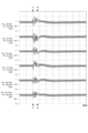
- the top three rows of Figure 31 are waveform diagrams showing the operation of the PWM modulator 3202.
- the modulation rate command ( ⁇ rf) from the modulation command calculation circuit 3203 is compared with the carrier wave in magnitude, and if the former is larger, the gate (GH) to the upper self-extinguishing element IGTH is energized, and if the former is smaller, the gate (GL) to the lower self-extinguishing element IGTL is energized. It is necessary to prevent the gates (GH) and (GL) from being energized simultaneously, as this could cause a capacitor short circuit accident due to the simultaneous current flowing through the upper and lower self-extinguishing elements.
- the unit converter current (Ib) flows from the negative terminal (D) to the positive terminal (C).
- the gate (GH) is energized during this period (from time t0 to t1, and from t2 to t3), the upper self-extinguishing element IGTH flows, and the converter output voltage (Vb) becomes the capacitor voltage (Vc).
- the unit converter current (Ib) becomes the discharge current (Ic ⁇ 0) of the capacitor 3201, so the capacitor voltage (Vc) drops.
- the unit converter current (Ib) flows from the positive terminal (C) to the negative terminal (D).
- the gate (GL) is energised during this period (from time t4 to t5, and from t6 onwards)
- the modulation command calculation circuit 3203 outputs a modulation command ( ⁇ rf) to the PWM modulator 3202.
- the modulation command ( ⁇ rf) is the time ratio of the gate (GH) activation period.
- the modulation command calculation circuit 3203 is required to have two functions. The first is to make the converter output voltage (Vb) follow the voltage command (Vcrf) obtained by dividing the voltage command (Vrf) of an arm consisting of K unit converters connected in series into K equal parts. The second is to make the deviation (Vcd) between the capacitor voltage measurement value (Vc_fB) and the average voltage (Vc_arm) of K capacitors in the same arm zero in order to maintain balance in the voltages of the K capacitors in the arm.
- the current sign detector 3204 checks the sign of the unit converter current (Ib), and when (Ib>0), the gain of the gain 3205 is made positive, and when the deviation (Vcd) is positive, the modulation command correction (Vcrf_add) is made positive to increase the modulation command ( ⁇ rf) and lower the converter output voltage (Vb).
- the gain of the gain 3205 is made negative, and when the deviation (Vcd) is positive, the modulation command correction (Vcrf_add) is made negative to decrease the modulation command ( ⁇ rf) and lower the converter output voltage (Vb).
- the gate (GL) is energized without the modulation command ( ⁇ rf) during the period (from time t0_s to t0_e) when the unit converter current (Ib) is positive and exceeds the set value (+Ib_s, +Ib_e), and the gate (GH) is energized without the modulation command ( ⁇ rf) during the period (from time t4_s to t4_e) when the unit converter current (Ib) is negative and its absolute value exceeds the set value (-Ib_s, -Ib_e).
- switching at current values that exceed the setting can be avoided.
- currents that exceed the setting are concentrated in the diode.
- diodes have a higher junction temperature tolerance than self-extinguishing elements such as IGBTs and IGCTs. This reduces the risk of equipment damage and allows continued operation.
- capacitor 3201 changes from discharge mode to open mode
- capacitor 3201 changes from open mode to charge mode.
- the capacitor voltage waveforms Vc0 and Vc in Figure 32 the capacitor voltage changes in an upward direction during both periods.
- the MMC converter of the present invention is capable of both miniaturizing the device and ensuring continued operation in the event of a system fault.
- FIG. 1 is a diagram showing the configuration of an MMC converter according to the present invention.
- FIG. 2 is a diagram showing a configuration of a leg circuit according to a first embodiment of the present invention.
- FIG. 3 is a diagram showing the configuration of a unit converter according to the present invention.
- FIG. 4 is a diagram showing a configuration of a power converter control device according to a first embodiment of the present invention.
- FIG. 5 is a diagram showing the configuration of a direct current control device according to a first embodiment of the present invention.
- FIG. 6 is a diagram showing the configuration of an AC current control device according to the present invention.
- FIG. 7 is a diagram showing the configuration of a circulating current control device according to a first embodiment of the present invention.
- FIG. 1 is a diagram showing the configuration of an MMC converter according to the present invention.
- FIG. 2 is a diagram showing a configuration of a leg circuit according to a first embodiment of the present invention.
- FIG. 3 is a diagram showing the configuration of
- FIG. 8 is a diagram showing the configuration of a first embodiment of a unit converter control device according to the present invention.
- FIG. 9 is a diagram showing the configuration of a power converter control device according to a second embodiment of the present invention.
- FIG. 10 is a diagram showing the configuration of a direct current control device according to a second embodiment of the present invention.
- FIG. 11 is a diagram showing the configuration of a positive/negative balance control device according to a second embodiment of the present invention.
- FIG. 12 is a diagram showing the configuration of a circulating current control device according to a second embodiment of the present invention.
- FIG. 13 is an explanatory diagram of a three-line ground fault condition and waveform measurement points in a two-circuit power transmission system during operation of the MMC converter of the present invention.
- FIG. 13 is an explanatory diagram of a three-line ground fault condition and waveform measurement points in a two-circuit power transmission system during operation of the MMC converter of the present invention.
- FIG. 14 is a diagram showing the accident occurrence time t1 and the circuit breaker operation time t2 in the event of a ground fault shown in FIG. 13, and the switching conditions of each part.
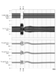
- FIG. 15 is a diagram showing AC voltage and current waveforms when a system fault occurs in the cases of FIGS. 13 and 14 and the capacitor average voltage of the unit converters of the six power arm circuits that make up the MMC converter in the second embodiment of the present invention, with the current suppression function during switching of the present invention excluded.
- FIG. 16 is a diagram showing the maximum and minimum capacitor values of the unit converters of the six power arm circuits that constitute the MMC converter when a system fault occurs in the cases of FIGS.
- FIG. 17 is a diagram showing AC voltage and current waveforms when the system fault of FIG. 13 and FIG. 14 occurs with the current suppression function during switching of the present invention operating in the MMC converter according to the second embodiment of the present invention, and also shows the capacitor average voltage of the unit converters of the six power arm circuits that make up the MMC converter.
- FIG. 18 is a diagram showing the maximum and minimum capacitor values of the unit converters of the six power arm circuits that constitute the MMC converter when a system fault occurs as shown in FIG. 13 and FIG. 14 with the current suppression function during switching of the present invention operating in the MMC converter according to the second embodiment of the present invention.
- FIG. 17 is a diagram showing AC voltage and current waveforms when the system fault of FIG. 13 and FIG. 14 occurs with the current suppression function during switching of the present invention operating in the MMC converter according to the second embodiment of the present invention, and also shows the capacitor average voltage of the unit converters of the six power arm circuits that make up the MMC converter.
- FIG. 18 is a diagram showing the
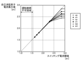
- FIG. 19 is a diagram showing a second embodiment of the MMC converter of the present invention, in which the vertical axis indicates the maximum value of the current of the 2 ⁇ K self-arc-suppressing elements constituting each arm of the six power arm circuits constituting the MMC converter, and the horizontal axis indicates the switching current setting value of the present invention.
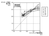
- FIG. 20 is a diagram showing a second embodiment of the MMC converter of the present invention, in which the vertical axis indicates the maximum value of the current of 2 ⁇ K anti-parallel diodes constituting each arm for each of the 66 power arm circuits constituting the MMC converter, and the horizontal axis indicates the switching current setting value of the present invention.
- FIG. 20 is a diagram showing a second embodiment of the MMC converter of the present invention, in which the vertical axis indicates the maximum value of the current of 2 ⁇ K anti-parallel diodes constituting each arm for each of the 66 power arm circuits constituting the MMC converter, and the horizontal axis indicates the switching current
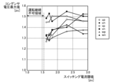
- FIG. 21 is a diagram showing a second embodiment of the MMC converter of the present invention, in which the vertical axis indicates the maximum value of the voltages of the K capacitors constituting each arm of the six power arm circuits constituting the MMC converter, and the horizontal axis indicates the switching current setting value of the present invention.
- FIG. 22 is a diagram showing a second embodiment of the MMC converter of the present invention, in which the vertical axis indicates the maximum value of the instantaneous voltage imbalance value (maximum value-minimum value) between the K capacitor voltages constituting each arm for each of the six power arm circuits constituting the MMC converter, and the horizontal axis indicates the switching current setting value of the present invention.
- FIG. 22 is a diagram showing a second embodiment of the MMC converter of the present invention, in which the vertical axis indicates the maximum value of the instantaneous voltage imbalance value (maximum value-minimum value) between the K capacitor voltages constituting each arm for each of the six power arm circuits constituting the MMC
- FIG. 23 is a diagram showing the configuration of a power converter control device according to a third embodiment of the present invention.
- FIG. 24 is a diagram showing the configuration of a positive/negative balance control device according to a third embodiment of the present invention.
- FIG. 25 is a diagram showing the configuration of a circulating current control device according to a third embodiment of the present invention.
- FIG. 26 is a diagram showing AC voltage and current waveforms when the system fault of FIG. 13 and FIG. 14 occurs with the current suppression function during switching of the present invention operating in the third embodiment of the MMC converter of the present invention, and the capacitor average voltage of the unit converters of the six power arm circuits that make up the MMC converter.
- FIG. 24 is a diagram showing the configuration of a positive/negative balance control device according to a third embodiment of the present invention.
- FIG. 25 is a diagram showing the configuration of a circulating current control device according to a third embodiment of the present invention.
- FIG. 26 is a diagram showing AC voltage and current waveforms when the
- FIG. 27 is a diagram showing the maximum and minimum capacitor values of the unit converters of the six power arm circuits that constitute the MMC converter when a system fault occurs as shown in FIG. 13 and FIG. 14 with the current suppression function during switching of the present invention operating in the MMC converter according to the third embodiment of the present invention.
- FIG. 28 is a diagram showing the configuration of a leg circuit according to a fourth embodiment of the present invention.
- FIG. 29A is a first diagram showing the configuration of Example 4 of the inductive element according to the present invention.
- FIG. 29B is a second diagram showing the configuration of the inductive element according to the fourth embodiment of the present invention.
- FIG. 30 is a diagram showing the configuration of a unit converter for explaining the means of the MMC converter of the present invention.
- FIG. 31 is a diagram showing operation waveforms of a conventional unit converter for explaining the means of the MMC converter of the present invention.
- FIG. 32 is a diagram showing operation waveforms of the unit converter of the present invention, for explaining the means of the MMC converter of the present invention.
- FIG. 1 is a diagram showing the configuration of a first embodiment of an MMC converter according to the present invention.
- the MMC converter 1 is an MMC converter, which is connected between the positive terminal (P) and negative terminal (N) of a DC power supply 101 and the three terminals (u, v, w) of a three-phase AC power supply 102.
- the MMC converter 1 has three leg circuits 2u, 2v, and 2w.
- the positive terminals (Pu, Pv, Pw) of the three leg circuits 2u, 2v, 2w are connected in a star configuration to the positive terminal (P) of the DC power supply 101, the negative terminals (Nu, Nv, Nw) are connected in a star configuration to the negative terminal (N) of the DC power supply 101, and the intermediate terminals (ACu, ACv, ACw) are connected to the three terminals (u, v, w) of the AC power supply 102.
- 103 is an AC sensor that outputs the voltage (Vac), reactive power (Qac), and reference phase ( ⁇ ) of the AC power supply 102.
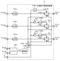
- FIG. 2 is a diagram showing the configuration of a leg circuit 2 (2u, 2v, 2w) according to a first embodiment of the present invention.
- x will be used to represent the three phases (u, v, w) of the AC power supply 102.
- Leg circuit 2 includes a two-terminal positive arm power circuit 21Px, a two-terminal negative arm power circuit 21Nx, a positive inductive element 22Px such as a reactor, a negative inductive element 22Nx, and two current transformers (23Px, 23Nx).
- the positive terminal (APx) of the positive arm power circuit 21Px is connected to the positive terminal (Px) of the leg circuit 2
- its negative terminal (BPx) is connected to the first terminal of the positive inductive element 22Px
- its second terminal is connected in parallel to the intermediate terminal (ACx) of the leg circuit 2 and the first terminal of the negative inductive element 22Nx.
- the second terminal of the negative inductive element 22Nx is connected to the positive terminal (ANx) of the negative arm power circuit 21Nx, and its negative terminal (BNx) is connected to the negative terminal (Nx) of the leg circuit 2.
- the positive side current transformer 23Px detects arm currents (I_up, I_vp, I_wp) whose positive sign is in the direction from the negative side terminal (BPx) to the positive side terminal (APx) of the positive side arm power circuit 21Px, and distributes and outputs them to the positive side arm control device 24Px and the power converter control device 4.
- the negative current transformer 23Nx detects the arm current (I_un, I_vn, I_wn) whose positive sign is in the direction from the positive terminal (ANx) to the negative terminal (BNx) of the negative arm power circuit 21Nx, and distributes and outputs it to the negative arm control device 24Nx and the power converter control device 4.
- the positive arm power circuit 21Px and the negative arm power circuit 21Nx each have K (K is a natural number of 2 or more) two-terminal unit converters 3 connected in series between their respective positive terminals (APx, ANx) and negative terminals (BPx, BNx).
- the positive arm control device 24Px is connected to the positive arm power circuit 21Px
- the negative arm control device 24Nx is connected to the negative arm power circuit 21Nx.
- the arm control device 24 consists of K unit converter control devices 8 and an average value calculator 201 that outputs the average value of K input signals.
- y will be used to represent the suffixes (P, N) of the two poles of the DC power supply 101.
- k will be used to represent the suffixes (1, 2, ..., K) of the K unit converters.
- the positive arm control device 24Px receives the arm voltage command (Vrf_xp) from the power converter control device 4 and branches off the reference phase ( ⁇ _x).
- the negative arm control device 24Nx receives the arm voltage command (Vrf_xn) from the power converter control device 4 and branches off the reference phase ( ⁇ _x).
- the arm control device 24 distributes and outputs the unit converter current (Ib) and the arm capacitor average voltage (Vc_xy) from the average value calculator 201 to the unit converter control devices 8 provided for each of the K unit converters 3. It also distributes and outputs the arm capacitor average voltage (Vc_xy_t) that is calculated by inputting the reference phase ( ⁇ _x) and calculating the moving average over the AC system period to the unit converter control devices 8.
- FIG. 3 is a diagram showing the configuration of the unit converter 3 according to the present invention.
- the unit converter 3 is equipped with a unit converter power circuit and a unit converter auxiliary circuit in a half-bridge power circuit configuration.
- the unit converter power circuit connects the positive electrode of the upper self-arc-extinguishing element 31H (the collector of the IGBT or the anode of the IGCT) to the positive electrode of the capacitor 32, and the negative electrode of the upper self-arc-extinguishing element 31H (the emitter of the IGBT or the cathode of the IGCT) to the positive terminal (C) of the unit converter 3 and the positive electrode of the lower self-arc-extinguishing element 31L in a branch connection.
- the negative electrode of the lower self-arc-extinguishing element 31L is branch-connected to the negative electrode of the capacitor 32 and the negative terminal (D) of the unit converter 3.
- An upper diode 33H is connected in anti-parallel to the upper self-arc-extinguishing element 31H.
- a half-bridge power circuit is formed by connecting a lower diode 33L in anti-parallel to the lower self-arc-extinguishing element 31L.
- the unit converter auxiliary circuit includes a gate driver 36, a capacitor voltage detector 34, and a voltage signal converter 35.
- the gate driver 36 receives gate control signals (GH, GL) from the positive arm controller 24Px and the negative arm controller 24Nx, converts their levels, and outputs gate pulses to the gate circuit of the upper self-extinguishing element 31H and the gate circuit of the lower self-extinguishing element 31L.
- the gate control signals (GH, GL) adjust the on/off period to adjust the terminal voltage (Vb) of the unit converter 3 to the required value through PWM modulation.
- the capacitor voltage detector 34 outputs the voltage of the capacitor 32 to the voltage signal converter 35, which converts it to a signal level to generate a voltage signal Vc.
- the unit converter 3 outputs the capacitor voltage signal Vc generated by the voltage signal converter 35 to the positive arm control device 24Px and the negative arm control device 24Nx as a capacitor voltage signal (Vc_xy_k).
- FIG. 4 is a diagram showing the configuration of a power converter control device 4 according to a first embodiment of the present invention.
- FIG. 4 is based on the configuration disclosed in Patent Document 6.
- 401 is an arm current calculator, which inputs the arm currents (I_up, I_vp, I_wp, I_un, I_vn, I_wn) from the current transformer 23, and calculates and outputs the AC currents (I_u, I_v, I_w) that flow from the AC power source 102 to the intermediate terminals (ACu, ACv, ACw) of the MMC converter 1, and the through currents (I_cu, I_cv, I_cw) that flow from the negative terminal (Nx) to the positive terminal (Px) of the leg circuit (2u, 2v, 2w). It also calculates and outputs the DC current (I_dc) from the positive terminal (P) of the MMC converter 1.
- the AC current (I_u, I_v, I_w) is calculated using equation (3).
- the through current (I_cu, I_cv, I_cw) is calculated using equation (4).
- the DC current (I_dc) is calculated using equation (5).
- Vc_ave the total capacitor average voltage (Vc_ave).
- Vc_up the capacitor arm average voltages (Vc_up, Vc_vp, Vc_wp, Vc_un, Vc_vn, Vc_wn) from the arm control device 24 and outputs the capacitor leg average voltages (Vc_u, Vc_v, Vc_w) of the leg circuit 2 and the capacitor positive-negative difference voltages (Vc_pnu, Vc_pnv, Vc_pnw). It also calculates and outputs the total capacitor average voltage (Vc_ave).
- the capacitor leg average voltages (Vc_u, Vc_v, Vc_w) are calculated using equation (6).
- Vc_pnu, Vc_pnv, Vc_pnw The capacitor positive/negative voltage difference (Vc_pnu, Vc_pnv, Vc_pnw) is calculated using equation (7).
- the total capacitor average voltage (Vc_ave) is calculated using equation (8).
- FIG. 6 is an AC current control device that inputs the AC current (I_u, I_v, I_w) from the arm current calculator 401, the reference phase ⁇ of the AC power source 102, and two-phase current commands (Irf_aq, Irf_ad), and outputs three-phase AC arm voltage command components (Vrf_au, Vrf_av, Vrf_aw).
- Vc_ave total capacitor average voltage
- Vcrf command value
- 404 is a reactive power regulator that inputs the reactive power (Qac) from the AC sensor 103 and the command value (Qacrf) and outputs it to the q-side input of the output switch 405.
- the 406 is an AC voltage regulator that inputs the voltage (Vac) from the AC sensor 103 and the command value (Vacrf) and outputs it to the V side input of the output switch 405.
- the output switch 405 selects the input signal from the reactive power regulator 404 connected to the q-side input or the input signal from the AC voltage regulator 406 connected to the v-side input, and outputs it to the AC current control device 6 as the reactive power component (Irf_ad) of the AC current command.
- a circulating current control device which receives the through current (I_cu, I_cv, I_cw) from the arm current calculator 401 and the three-phase current commands (Irf_cu, Irf_cv, Irf_cw) and outputs the three-phase arm voltage command circulating component (Vrf_cu, Vrf_cv, Vrf_cw). It also outputs the zero-phase component (Irf_c0) obtained by performing a three-phase to three-phase conversion on the three-phase current commands (Irf_cu, Irf_cv, Irf_cw). Details of the three-phase to three-phase conversion performed on the three-phase current commands (Irf_cu, Irf_cv, Irf_cw) will be described later.
- Vc_pnu, Vc_pnv, Vc_pnw positive/negative difference voltage
- Irf_pnu, Irf_pnv, Irf_pnw three-phase current commands
- the limiter 408 is an inter-leg balance control device that performs proportional integral calculations so that the leg voltage deviation (Vc_bu, Vc_bv, Vc_bw), which is the difference between the leg average voltage (Vc_u, Vc_v, Vc_w) from the capacitor voltage calculator 402 and the output of limiter 409, which inputs the total capacitor average voltage (Vc_ave), becomes zero, and outputs three-phase current commands (Irf_bu, Irf_bv, Irf_bw).
- the limiter 409 outputs a limiter detection signal (Sw_lmt) at level 1 when the total capacitor average voltage (Vc_ave) reaches the limit value.
- 410 is an arm voltage command calculator that energizes the three-phase arm voltage command AC components (Vrf_au, Vrf_av, Vrf_aw) from the AC current control device 6, the three-phase arm voltage command circulating components (Vrf_cu, Vrf_cv, Vrf_cw) from the circulating current control device 7, and the three-phase voltage commands (Vrf_du, Vrf_dv, Vrf_dw) that are the three-branched outputs of the DC voltage command (Vrf_dc) from the DC current control device 5 for each phase, and outputs arm voltage commands (Vrf_up, Vrf_un, Vrf_vp, Vrf_vn, Vrf_wp, Vrf_wn).
- the arm voltage commands (Vrf_up, Vrf_un, Vrf_vp, Vrf_vn, Vrf_wp, Vrf_wn) are calculated using equation (10).
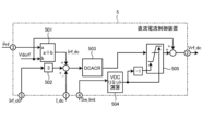
- FIG. 5 is a diagram showing the configuration of a first embodiment of a direct current control device 5 according to the present invention.
- the divider 501 inputs the active power command (Prf) and the DC voltage command (Vdcrf) and outputs the DC current command (Irf_dc).
- the zero-phase component current command (Irf_c0) from the power converter control device 4 is converted to a DC component command by the gain 502.
- the DC component command output by the gain 505 is applied to the DC current command (Irf_dc) output by the divider 501, and is compared with the DC current (I_dc) and input to the DC current regulator 503.
- the DC current regulator 503 is configured as a proportional-integral controller or a proportional controller.
- a proportional-integral controller can be used for the DC current regulator 503 of one of the MMC converters.
- the remaining side must be a proportional controller without an integral element.
- the DC voltage limiter 504 commands the DC voltage command limiter 505 to limit and output the command value from the DC current regulator 503.
- the command value output by the DC voltage command limiter 505 is biased with a DC voltage command (Vdcrf) and is output as the arm voltage command DC component (Vrf_dc).
- FIG. 6 is a diagram showing the configuration of an AC current control device 6 according to the present invention.
- 601 is a three-phase to two-phase converter that converts AC currents (I_u, I_v, I_w) into two-phase currents (I_aq, I_ad) at the reference phase ⁇ of the AC power source 102, matches them with two-phase AC current commands (Irf_aq, Irf_ad), and inputs them to a proportional-integral controller 602.
- the three-phase to two-phase converter 601 calculates the relationship between the input and output in equation (11).
- Vrf_aq, Vrf_ad two-phase voltage commands
- Vrf_au, Vrf_av, Vrf_aw three-phase arm voltage command AC components
- the two-phase to three-phase inverter 603 calculates the relationship between the input and output of equation (12).
- FIG. 7 is a diagram showing the configuration of a circulating current control device 7 according to the present invention.
- 701 is a three-phase to three-phase converter that inputs current commands (Irf_cu, Irf_cv, Irf_cw) and converts them into three-phase current commands (Irf_c ⁇ , Irf_c ⁇ , Irf_c0) including the zero phase.
- the three-phase to three-phase converter 701 calculates the relationship between the input and output of equation (13).
- 702 is a three-phase to two-phase converter that converts through currents (I_cu, I_cv, I_cw) into two-phase circulating currents (I_c ⁇ , I_c ⁇ ).
- the three-phase to two-phase converter 702 calculates the relationship between the input and output of equation (14).
- the two components other than the zero-phase component are matched with the two-phase circulating currents (I_c ⁇ , I_c ⁇ ) and input to the proportional-integral controller 703.
- Vrf_c ⁇ , Vrf_c ⁇ the two-phase voltage commands
- Vrf_cu, Vrf_cv, Vrf_cw three-phase arm voltage command AC components
- the two-phase to three-phase inverter 704 calculates the relationship between the input and output of equation (15).
- FIG. 8 is a diagram showing the configuration of a unit converter control device 8 according to a first embodiment of the present invention.
- the arm voltage command (Vrf_xy) output from the power converter control device 4 for each arm power circuit 21 is multiplied by 1/K to generate a unit converter voltage command (Vcrf_xy).
- Vc_xy capacitor arm average voltage signal
- Vc_xy_t capacitor arm moving average voltage signal
- the capacitor voltage signal (Vc_xy_k) is matched with the output of the signal switcher 802 to generate the capacitor voltage deviation (Vcd_xy_k).
- Vc_xy_k capacitor voltage signal
- the current sign detector 804 detects the sign of the unit converter current (Ib_xy), and when the unit converter current (Ib_xy) has a positive sign, the gain of the gain 805 is switched to positive, and when the unit converter current (Ib_xy) has a negative sign, the gain of the gain 805 is switched to negative.
- the output of this gain 805 is biased to the unit converter voltage command (Vcrf_xy) and input to the divider 801.
- the divider 801 outputs the modulation rate command ( ⁇ rf_xy_k) obtained by normalizing the unit converter voltage command (Vcrf_xy) after the output of the gain 805 is activated with the capacitor arm average voltage signal (Vc_xy) or the capacitor arm moving average voltage signal (Vc_xy_t).
- ⁇ rf modulation rate signal
- ⁇ rf_xy_k the input modulation rate command
- 808 is a carrier wave output device that outputs a triangular wave with a maximum value of 1 and a minimum value of 0 as a carrier wave to comparator 807.
- the comparator 807 sets the output signal (GH) to level 1 and the output signal (GL) to level 0 and outputs them.
- the comparator 807 sets the output signal (GH) to level 0 and the output signal (GL) to level 1 and outputs them.
- the switching current limiter 809H and 809L are switching current limiters. During normal operation, when the unit converter current (Ib_xy) does not exceed the threshold value described below, the switching current limiter 809H outputs the output signal (GH) as is, and the switching current limiter 809L outputs the output signal (GL) as is.
- 810H and 810L are pulse rise delay circuits that ensure a dead time determined by the characteristics of the self-extinguishing element 31 and diode 33 of the unit converter 3 shown in Figure 3, thereby preventing a short circuit of the capacitor 32.
- 811H and 811L are rise detection circuits that input the rise detection results of the outputs of the pulse rise delay circuits 810H and 810L to the pulse width securing circuits 812H and 812L to secure the level 1 period of the minimum ignition time determined by the characteristics of the self-extinguishing element 31 and diode 33, preventing damage to the self-extinguishing element 31 and diode 33 due to incomplete switching.
- the outputs of the pulse rise delay circuits 810H and 810L and the outputs of the pulse width securing circuits 812H and 812L are input to logical sum circuits 813H and 813L, which alternately output on and off the gate control command (GH_xy_k) to the upper self-extinguishing element (31H) and the gate control command (GL_xy_k) to the lower self-extinguishing element (31L).
- a comparator with hysteresis that switches the output (SH_H) from level 0 to level 1 when the unit converter current (Ib_xy) exceeds the set value (Ib_s) in the positive direction, and switches from level 1 to level 0 when it falls below a positive set value (Ib_e) whose absolute value is smaller than the set value (Ib_s).
- ⁇ 815 is a comparator with hysteresis that switches the output (SH_L) from level 0 to level 1 when the unit converter current (Ib_xy) falls below the set value (-Ib_s) in the negative direction, and switches from level 1 to level 0 when it exceeds the set value (-Ib_e).
- a mode switch 816 is a mode switch that exclusively outputs a mode switching signal (MOD_H) to level 1 when the output (SW_H) of the comparator with hysteresis 814 is at level 1, and exclusively outputs a mode switching signal (MOD_L) to level 1 when the output (SW_L) of the comparator with hysteresis 815 is at level 1.
- MOD_H mode switching signal
- MOD_L mode switching signal
- the switching current limiter 809H When the mode switching signal (MOD_H) is at level 1, the switching current limiter 809H outputs a fixed level 1, and the switching current limiter 809L outputs a fixed level 0.
- the switching current limiter 809L When the mode switching signal (MOD_L) is at level 1, the switching current limiter 809L outputs a fixed level 1, and the switching current limiter 809H outputs a fixed level 0.
- Example 1 The above configuration of Example 1 can solve the problem.
- the positive terminal (Px) of leg circuit 2 is connected in the following order: positive arm power circuit 21Px, positive inductive element 22Px, intermediate terminal (ACx) of leg circuit 2, negative inductive element 22Nx, negative arm power circuit 21Nx, and negative terminal (Nx) of leg circuit 2.
- the arm power circuits and inductive elements may be rearranged and connected in the following order: from the positive terminal (Px) of leg circuit 2 to the positive inductive element 22Px, the positive arm power circuit 21Px, the intermediate terminal (ACx) of leg circuit 2, the negative arm power circuit 21Nx, the negative inductive element 22Nx, and the negative terminal (Nx) of leg circuit 2.
- the output switch 405 selects the output of the reactive power regulator 404 as the reactive power component (Irf_ad) of the AC current command, it has the effect of relatively easily suppressing the overcurrent flowing through the MMC converter in the event of a grid accident.
- the output switch 405 selects the output of the AC voltage regulator 406, it has the effect of contributing to the stability of the grid by quickly supplying reactive power in the event of a voltage drop caused by a grid accident, just like conventional commercial power generation equipment.
- control is performed using the instantaneous capacitor voltage signal (Vc_xy_k) and the capacitor arm average voltage signal (Vc_xy), thereby realizing control with fast response.
- Vc_xy_k instantaneous capacitor voltage signal
- Vc_xy capacitor arm average voltage signal
- the reference value of the capacitor voltage deviation (Vcd_xy_k) between the unit converters 3 and the reference value for normalizing the modulation factor command ( ⁇ rf_xy_k) can be the capacitor arm moving average voltage signal (Vc_xy_t) with small temporal fluctuations, so that the operation of the unit converter control device 8 is stable when a system fault spreads, and it is possible to prevent the unit converter control device 8 from being unnecessarily limited by the limiter 806 and becoming stuck at the upper and lower limits, resulting in an uncontrollable state.
- the modulation rate signal ( ⁇ rf) is limited between the maximum value ⁇ max and the minimum value ⁇ min by the limiter 806, so that short-term gate control commands (GH_xy_k, GL_xy_k) that would damage the self-extinguishing element 31 and the diode 33 can be prevented.
- the mode switcher 816 changes the level of the mode switching signal (MOD_H, MOD_L) in a short time, thereby extending the operation delay time of the downstream pulse rise delay circuit 810 and pulse width securing circuit 812, thereby preventing problems that impair operational continuity in the event of a system accident.
- a gate control command (GL_xy_k) to the lower self-extinguishing element (31L) is activated regardless of the modulation factor command ( ⁇ rf_xy_k) to extinguish the gate control command (GL_xy_k) to the upper self-extinguishing element (31H), and during the period when the unit converter current input (Ib) is below the negative set value (-Ib_s), a gate control command (GL_xy_k) to the upper self-extinguishing element (31H) is activated regardless of the modulation factor command ( ⁇ rf_xy_k).
- the absolute current value during switching is suppressed to a set value (Ib_s) or less, and the total capacitor average voltage (Vc_ave) that rises due to the operation of the unit converter control device 8 is output to the AC current control device 6 by adjusting the active power component (Irf_aq) of the AC current command in the capacitor voltage regulator 403, and the AC current control suppresses the capacitor voltage rise, thereby achieving the objective.
- FIG. 9 is a diagram showing the configuration of a power converter control device according to a second embodiment of the present invention.
- FIG. 9 is based on the configuration disclosed in Patent Document 7.
- the same numbers are used for components common to the power converter control device 4 shown in Figure 4. Explanations of components with the same numbers as in the previous Figure 4 will be omitted to avoid duplication.
- the MMC converter of Example 2 has a configuration in which the power converter control device 4 of the MMC converter of Example 1 is replaced with a power converter control device 9, and explanations of components other than the power converter control device 9 will be omitted.
- a DC current control device 10, which will be described later, is connected to the power converter control device 9.
- the power converter control device 9 outputs a DC current (I_dc) to the DC current control device 10 and inputs a DC voltage command (Vrf_dc) from the DC current control device 10.
- the power converter control device 9 includes a positive/negative balance control device 11, a circulating current control device 12, a leg balance control device 901, and adders 902 and 903.
- the positive/negative balance control device 11 inputs the positive/negative difference voltage (Vc_pnu, Vc_pnv, Vc_pnw) from the capacitor voltage calculator 402, the two-phase AC current command values (Irf_aq, Irf_ad), and the reference phase ( ⁇ ), and outputs three-phase circulating current commands (Irf_cu, Irf_cv, Irf_cw).
- the circulating current control device 12 inputs the through current (I_cu, I_cv, I_cw), three-phase circulating current commands (Irf_cu, Irf_cv, Irf_cw), and double the reference phase angle (2 ⁇ ), and outputs three-phase arm voltage command circulating components (Vrf_cu, Vrf_cv, Vrf_cw).
- the leg balance control device 901 performs proportional integral calculations so that the leg voltage deviations (Vc_bu, Vc_bv, Vc_bw) become zero, and outputs the three-phase arm voltage command leg balance components (Vrf_bu, Vrf_bv, Vrf_bcw).
- the arm voltage command calculator 410 and adders 902 and 903 output arm voltage commands (Vrf_up, Vrf_un, Vrf_vp, Vrf_vn, Vrf_wp, Vrf_wn).
- the arm voltage commands (Vrf_up, Vrf_un, Vrf_vp, Vrf_vn, Vrf_wp, Vrf_wn) are calculated using equation (16).
- FIG. 10 is a diagram showing the configuration of a second embodiment of a direct current control device 10 according to the present invention.
- Components common to the direct current control device 5 according to the first embodiment shown in FIG. 5 are given the same numbers. To avoid duplication, explanations of components with the same numbers as those in the direct current control device 5 according to the first embodiment shown in FIG. 5 are omitted.
- 1001 is an adder that inverts the sign of the output of the DC current regulator 503, activates it as a DC voltage command (Vdcrf), and outputs it as the arm voltage command DC component (Vrf_dc_fc) to another MMC converter (not shown in Figure 1) that is connected behind the DC terminals (P, N) of the MMC converter 1.
- Vdcrf DC voltage command
- Vrf_dc_fc arm voltage command DC component
- FIG. 11 is a diagram showing the configuration of a second embodiment of the positive/negative balance control device 11 according to the present invention.
- the positive-negative difference voltage (Vc_pnu, Vc_pnv, Vc_pnw) from the capacitor voltage calculator 402 is input to gains 1101u, 1101v, and 1101w.
- the reference phase ( ⁇ ) is shifted in the order of each phase and input to cosine wave generators 1102u, 1102v, and 1102w.
- the outputs of gains 1101u, 1101v, 1101w and the outputs of cosine wave generators 1102u, 1102v, 1102w are input to the first input terminal (a) and second input terminal (b) of multipliers 1103u, 1103v, 1103w for each phase.
- 1105 is an absolute value calculator that outputs the vector absolute value of the two-phase AC current command values (Irf_aq, Irf_ad) and inputs it to a function generator 1106, whose output is input to the first terminal of a switch 1104.
- the second terminal of the switch 1104 is branched and input to the third input terminal (c) of the multipliers 1103u, 1103v, and 1103w.
- the open/close signal of the switch 1104 is input to the multipliers 1103u, 1103v, and 1103w.
- Multipliers 1103u, 1103v, and 1103w output the multiplication result (a x b x c) of the first to third inputs when switch 1104 is closed, and output the multiplication result (a x b) of the first and second inputs when switch 1104 is open.
- multipliers 1103u, 1103v, and 1103w are output as three-phase current commands (Irf_cu, Irf_cv, Irf_cw).
- FIG. 12 is a diagram showing the configuration of a circulating current control device 12 according to a second embodiment of the present invention.
- 1201 and 1202 are three-phase to two-phase converters that convert the current commands (Irf_cu, Irf_cv, Irf_cw) and through currents (I_cu, I_cv, I_cw) of each of the three phases into two-phase circulating current commands (Irf_cq, Irf_cd) and circulating currents (I_cq, I_cd) at twice the angle (2 ⁇ ) of the reference phase ( ⁇ ), and match them for each phase before inputting them to the proportional-integral controller 1203.
- the three-phase to two-phase converters 1201 and 1202 calculate the input-output relationship of equations (17) and (18).
- Vrf_cq, Vrf_cd two-phase voltage commands
- Vrf_cu, Vrf_cv, Vrf_cw three-phase arm voltage command AC components
- the two-phase to three-phase inverter 1204 calculates the relationship between the input and output of equation (19).
- Example 2 The above configuration of Example 2 can solve the problem.
- the output of the positive/negative balance control device 11 is directly connected to the circulating current control device 12 for current feedback control, and the leg balance control device 901 biases the output side of the current feedback control for feedforward control.
- the positive/negative balance control device 407 and the leg balance control device 408 both input a linear combination of the arm average voltages of six capacitors, but use input signals of opposite signs for both, and the outputs are parallel-energized and input to the circulating current control device 7, so cancellation of the effects between the two is unavoidable.
- the linear combination of the capacitor arm average voltages, which serves as the input signal includes coefficients of positive and negative signs, so it is not practical to make use of the integral gain.
- the above-described configuration of the power converter control device 9 separates the positive/negative balance control device 11 into current feedback control and the leg balance control device 901 into feedforward control, which has the effect of adjusting both to a deviation of 0 using control that includes an integral term.
- the above-described configuration of the DC current control device 10 differs from the DC current control device 5 in that it is independent of the zero-phase component output (Irf_c0) of the circulating current control device 7.
- the DC current regulator 503 is shared by two MMC converters, and the adder 1001 branches out and outputs the DC voltage command (Vrf_dc) and the DC voltage command (Vrf_dc_fc) to another MMC converter, which has the effect of realizing a DC current control device 10 for two MMC converters with the minimum equipment configuration.
- the amplitude of the three-phase circulating current commands (Irf_cu, Irf_cv, Irf_cw) can be adjusted using the absolute value calculator 1105 and function generator 1106 in addition to the positive/negative voltage difference (Vc_pnu, Vc_pnv, Vc_pnw) and reference phase ( ⁇ ), so that near the rated current, the circulating current command amplitude is adjusted according to the AC current command amplitude, keeping the circulating current to a necessary minimum, suppressing losses due to the circulating current and increasing the efficiency of the MMC converter.
- the output of the proportional-integral controller 1203 is handled by the integral term during steady-state operation, so that a wide fluctuation range can be secured for the proportional component that requires an immediate response in a transient state where the output is restricted by the limiter. This has the effect of realizing a high-speed response of the circulating current control device 12.
- Figure 13 shows a case where the DC ends of two MMC converters 1301 and 1302 are connected back-to-back to form a frequency converter.
- the delta winding of transformer 1303 is connected to the AC end of MMC converter 1301.
- the other terminal of transformer 1303 is connected to the trailing end of double-circuit transmission line 1304.
- a synchronous machine 1305 is connected to the AC end of the MMC converter 1302 to output a variable frequency, and a turbomachine (pump turbine) 1306 is directly connected to the rotating shaft.
- a turbomachine pump turbine
- the two-circuit transmission line 1304 is composed of leading end circuit breakers 52F1 and 52F2 and trailing end circuit breakers 52B1 and 52B2.
- the three phases of the first circuit are referred to as (1A, 1B, 1C)
- the three phases of the second circuit are referred to as (2A, 2B, 2C).
- a time chart is shown in FIG. 14.
- the time chart in FIG. 14 shows the operation of leading end circuit breakers 52F1 and 52F2 and trailing end circuit breakers 52B1 and 52B2 when a ground fault occurs in the double-circuit transmission line 1304 in FIG. 13.
- a three-phase ground fault occurs in the first circuit at the close end of the transformer 1303, causing 73 to short circuit.
- leading end circuit breaker 52F1 and trailing end circuit breaker 52B1 of the first circuit operate to open the circuit.
- the impedance of the transformer 1303 is set to 6% based on the capacity of the MMC converter 1302.
- This impedance value corresponds to the MMC converter described in Patent Document 8, and is the value when the capacity of the MMC converter is made smaller than the capacity of the existing synchronous machine 1305 and transformer 1303.
- the impedance converted into the self-capacity of the MMC converter 1302 is smaller than that of a transformer in a normal commercial power generation facility, so the overcurrent value when a system earth fault spreads is larger.
- the change in the capacitor voltage of the MMC converter is also large, which is a severe condition to consider.
- the generator Before the earth fault occurred, the generator was operating at rated output and rated power factor (lag 0.95).
- the peak value of the arm currents (I_up, I_vp, I_wp, I_un, I_vn, I_wn) of the MMC converter 1302 is 1, the peak value of the AC component of the arm current is 0.7, and the DC component is 0.3.
- Figures 15 and 16 show waveforms when the switching current threshold (Ib_s) of the hysteresis comparators 814 and 815 of the unit converter control device 8 according to the second embodiment of the present invention shown in Figure 8 is set to 2.85 times the rated arm current or more and the switching current is not limited.
- Ib_s switching current threshold
- Figures 17 and 18 show waveforms when the switching current threshold (Ib_s) of the hysteresis comparators 814 and 815 of the unit converter control device 8 according to the second embodiment of the present invention shown in Figure 8 is set to 1.8 times the rated arm current, limiting the switching current.
- Ib_s switching current threshold
- Figures 15 and 17 show the waveforms of the phase voltages (V_AN, V_BN, V_CN) on the transmission line side of the transformer 1303 and the AC currents (I_u, I_v, I_w) on the MMC converter 1301 side normalized to the rated values.
- the peak current (I_u, I_v, I_w) during the period from the occurrence of a ground fault at time t1 to the operation of the circuit breaker at time t2 reaches three times the rated current when the switching current is not limited in Fig. 15, whereas it is suppressed to 2.5 times the rated current when the switching current is limited in Fig. 17.
- Figures 19 to 22 show the change in characteristics when the switching current threshold (Ib_s) is gradually lowered from 2.85 times.
- the switching current threshold (Ib_s) has a lower limit, and if it is set below 1.55 times, the capacitor voltage balance cannot be maintained and the MMC converter 1302 cannot continue to operate.
- Figure 19 shows the switching current threshold (Ib_s) and the maximum value of the self-extinguishing element (31H, 31L) current for each of the six arms.
- Figure 20 shows the switching current threshold (Ib_s) and maximum value of the anti-parallel diode (33H, 33L) current for each of the six arms.
- the current of the anti-parallel diodes (31H, 31L) increases even after switching from the self-extinguishing element to the anti-parallel diode at the switching current threshold (Ib_s), and therefore exceeds the switching current threshold (Ib_s), unlike the current of the self-extinguishing element, as shown in Figure 20.
- the maximum value of the current of the anti-parallel diodes (33H, 33L) decreases with the switching current threshold (Ib_s).
- the switching current threshold (Ib_s) in the second embodiment of the present invention based on the maximum value of the current of the self-extinguishing elements (31H, 31L) shown in FIG. 19, not only is it possible to prevent damage to the self-extinguishing elements (31H, 31L) by suppressing the switching current, but it is also possible to suppress the maximum current value, thereby suppressing the rise in junction temperature and improving reliability, and it is also possible to increase the capacity of the device using the same self-extinguishing elements (31H, 31L) or to reduce the size of the self-extinguishing elements (31H, 31L).
- the switching current threshold (Ib_s) in the second embodiment of the present invention based on the maximum current value of the anti-parallel diodes (33H, 33L) shown in FIG. 20, not only is it possible to prevent damage to the anti-parallel diodes (33H, 33L) by suppressing the switching current, but it is also possible to suppress the maximum current value, thereby suppressing the rise in junction temperature and improving reliability, and it is also possible to increase the capacity of the device using the same anti-parallel diodes (33H, 33L) or reduce the size of the anti-parallel diodes (33H, 33L).
- FIG. 23 is a diagram showing the configuration of a power converter control device 25 according to a third embodiment of the present invention.
- the same numbers are used for components common to the power converter control device 4 shown in FIG. 4.
- the same numbers are used for components common to the power converter control device 9 shown in FIG. 9. Explanations of components with the same numbers as those in the previous FIGS. 4 and 9 are omitted to avoid duplication.
- the MMC converter of Example 3 has a configuration in which the power converter control device 4 of the MMC converter of Example 1 is replaced with a power converter control device 25, and explanations of components other than the power converter control device 25 are omitted.
- the power converter control device 25 is equipped with a positive/negative balance control device 26 and a circulating current control device 27.
- the positive/negative balance control device 26 inputs the positive/negative difference voltage (Vc_pnu, Vc_pnv, Vc_pnw) and the reference phase ( ⁇ ) from the capacitor voltage calculator 402, and outputs two-phase circulating current commands (Irf_cq, Irf_cd).
- the circulating current control device 27 inputs the through current (I_cu, I_cv, I_cw), two-phase circulating current commands (Irf_cq, Irf_cd), and double the reference phase angle (2 ⁇ ), and outputs three-phase arm voltage command circulating components (Vrf_cu, Vrf_cv, Vrf_cw).
- FIG. 24 is a diagram showing the configuration of a third embodiment of a positive/negative balance control device 26 according to the present invention.
- the positive-negative difference voltage (Vc_pnu, Vc_pnv, Vc_pnw) from the capacitor voltage calculator 402 is input to the moving average calculators 2401u, 2401v, 2401w, and the reference phase ( ⁇ ) is input to the one-period calculation counter 2402.
- the one-period calculation counter 2402 calculates one period of the AC power supply, and the moving average calculators 2401u, 2401v, 2401w calculate one-period moving averages (Vc_pnu_t, Vc_pnv_t, Vc_pnw_t) of the positive-negative difference voltage (Vc_pnu, Vc_pnv, Vc_pnw) based on the calculation result by the one-period calculation counter 2402, and input the one-period moving averages to the three-phase to two-phase converter 2403.
- the three-phase to two-phase converter 2403 calculates the relationship between the input and output of equation (20).
- the output (Vc_pnq_t, Vc_pnd_t) of the three-phase to two-phase converter 2403 is input to the proportional-integral controller 2404, which outputs the two-phase circulating current command values (Irf_cq, Irf_cd).
- FIG. 25 is a diagram showing the configuration of a circulating current control device 27 according to a third embodiment of the present invention.
- the two-phase circulating current commands (Irf_cq, Irf_cd) and circulating currents (I_cq, I_cd) are matched for each phase and input to the proportional-integral controller 2501.
- the two-phase voltage commands (Vrf_cq, Vrf_cd) from the proportional-integral controller 2501 are input to the two-phase to three-phase inverter 1204, which outputs the three-phase arm voltage command AC components (Vrf_cu, Vrf_cv, Vrf_cw).
- Example 3 The above configuration of Example 3 can solve the problem.
- the moving average value (Vc_pnu_t, Vc_pnv_t, Vc_pnw_t) of the positive/negative difference voltage for one period of the AC power supply frequency input to the three-phase to two-phase converter 2403 becomes DC in a steady state, which has the effect of enabling stable operation even if the measurement period of the capacitor average voltage of each arm and the calculation period of the moving average are lengthened. This has the effect of enabling this to be realized with inexpensive control devices and communication devices.
- the output of the proportional-integral controller 2501 is handled by the integral term during steady-state operation, so that a wide fluctuation range can be ensured for the proportional component that requires immediate response in a transient state where the output is limited by the limiter. This has the effect of realizing a high-speed response of the circulating current control device 27.
- a frequency converter is constructed by connecting the DC ends of two MMC converters 1301 and 1302 shown in the previous Figure 13 back to back, and the power converter control device 25 of the third embodiment of the present invention is used instead of the power converter control device 9 of the second embodiment of the present invention.
- the effects of the third embodiment of the present invention will be explained using the transient phenomenon when a near-end three-phase ground fault occurs in the time chart shown in the previous Figure 14. To avoid duplication, the explanations of Figures 13 and 14 will be omitted.
- FIG. 26 shows the waveforms of the phase voltages (V_AN, V_BN, V_CN) on the transmission line side of the transformer 1303 and the AC currents (I_u, I_v, I_w) on the MMC converter 1301 side, normalized to the rated values.
- the lower part of Figure 26 shows the average capacitor voltages of each arm (Vc_up, Vc_vp, Vc_wp, Vc_un, Vc_vn, Vc_wn) normalized by the rated voltage of the capacitor.
- Example 3 of the present invention has the same effect as Example 2 of the present invention.
- the above-described configuration of the power converter control device 25 makes it possible to suppress the switching current and the rise in the capacitor voltage, thereby achieving the objective.
- FIG. 28 shows the configuration of a fourth embodiment of a leg circuit 28 according to the present invention.
- leg circuit 2 shown in Figure 2 The same components as those in leg circuit 2 shown in Figure 2 are given the same numbers. Explanations of components with the same numbers as those in the previous Figure 2 are omitted to avoid duplication.
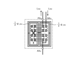
- FIGS. 29A and 29B are diagrams showing the configuration of a three-terminal inductive element 2801 according to the present invention.
- FIG. 29A shows the case where an alternating current (I_u) flows
- FIG. 29B shows the case where a through current (I_cu) flows.
- the configuration of the three-terminal inductive element 2801 is based on Patent Document 2. The configuration will be explained below using the u-phase as an example.
- the AC current (I_u) that flows from the intermediate terminal (AXu) of the three-terminal inductive element 2801 is split into two, one into a positive winding and one into a negative winding that are wound concentrically around the air gapped iron core legs, and flows from the positive terminal (PXu) and the other into the negative terminal (Nxu).
- the magnetic flux ( ⁇ _au) generated by the AC current (I_u) passes through the air gapped iron core legs and circulates through the air gap surrounded by the positive and negative windings.
- the magnetic flux ( ⁇ _cu) caused by the through current (I_cu) circulates through the air gap core leg and the auxiliary core leg.
- the magnetic path of the magnetic flux ( ⁇ _au) caused by the AC current (I_u) has a larger magnetic resistance than the magnetic path of the magnetic flux ( ⁇ _cu) caused by the through current (I_cu), because the air gap length in the magnetic path length is longer by the height of the iron core (h).
- the inductance for the AC current (I_u) is smaller than the inductance for the through current (I_cu).
- the former can be made 0.05 to 0.1 times the latter.
- the inductance for the through current (I_cu) is an indispensable inductive element for controlling the current in the MMC converter 1.
- the inductance for the AC current (I_u) is added to the inductance of the transformer that constitutes the AC power supply or the armature winding leakage inductance of the AC rotating electrical machine to suppress the AC current.
- the waveforms shown in Figures 15 to 22 have a transformer impedance of 6% and an inductive element impedance to AC current of less than 0.5%.
- the configuration of the three-terminal inductive element 2801 shown in Figures 29A and 29B makes the leakage magnetic flux of the positive winding and the negative winding equal, and the leakage inductance values equal.
- the leakage inductance imbalance between the positive winding and the negative winding can cause interference between AC current control and circulating current control. It can also cause non-theoretical harmonics.
- the three-terminal inductive element 2801 configuration shown in Figures 29A and 29B ensures non-interference between AC current control and circulating current control, and has the effect of suppressing the occurrence of non-theoretical harmonics.
Landscapes
- Engineering & Computer Science (AREA)
- Power Engineering (AREA)
- Rectifiers (AREA)
Priority Applications (3)
| Application Number | Priority Date | Filing Date | Title |
|---|---|---|---|
| PCT/JP2023/001587 WO2024154308A1 (ja) | 2023-01-19 | 2023-01-19 | モジュラー・マルチレベル電力変換器 |
| EP23917521.9A EP4654456A1 (en) | 2023-01-19 | 2023-01-19 | Modular multi-level electric power converter |
| JP2024571551A JPWO2024154308A1 (https=) | 2023-01-19 | 2023-01-19 |
Applications Claiming Priority (1)
| Application Number | Priority Date | Filing Date | Title |
|---|---|---|---|
| PCT/JP2023/001587 WO2024154308A1 (ja) | 2023-01-19 | 2023-01-19 | モジュラー・マルチレベル電力変換器 |
Publications (1)
| Publication Number | Publication Date |
|---|---|
| WO2024154308A1 true WO2024154308A1 (ja) | 2024-07-25 |
Family
ID=91955672
Family Applications (1)
| Application Number | Title | Priority Date | Filing Date |
|---|---|---|---|
| PCT/JP2023/001587 Ceased WO2024154308A1 (ja) | 2023-01-19 | 2023-01-19 | モジュラー・マルチレベル電力変換器 |
Country Status (3)
| Country | Link |
|---|---|
| EP (1) | EP4654456A1 (https=) |
| JP (1) | JPWO2024154308A1 (https=) |
| WO (1) | WO2024154308A1 (https=) |
Cited By (1)
| Publication number | Priority date | Publication date | Assignee | Title |
|---|---|---|---|---|
| WO2026062796A1 (ja) * | 2024-09-18 | 2026-03-26 | 日立三菱水力株式会社 | モジュラー・マルチレベル電力変換器 |
Citations (10)
| Publication number | Priority date | Publication date | Assignee | Title |
|---|---|---|---|---|
| JP5189105B2 (ja) | 2006-12-08 | 2013-04-24 | シーメンス アクチエンゲゼルシヤフト | 電流変換装置 |
| JP5197623B2 (ja) | 2006-12-08 | 2013-05-15 | シーメンス アクチエンゲゼルシヤフト | エネルギー蓄積器が配分されたモジュール式コンバータ |
| WO2015178376A1 (ja) * | 2014-05-21 | 2015-11-26 | 三菱電機株式会社 | 直流送電電力変換装置および直流送電電力変換方法 |
| JP6243083B2 (ja) | 2015-02-25 | 2017-12-06 | 日立三菱水力株式会社 | 可変速発電電動装置および可変速発電電動システム |
| WO2018211624A1 (ja) * | 2017-05-17 | 2018-11-22 | 三菱電機株式会社 | 電力変換装置 |
| JP6618823B2 (ja) | 2016-02-09 | 2019-12-11 | 株式会社東芝 | 電力変換装置 |
| WO2021182460A1 (ja) * | 2020-03-11 | 2021-09-16 | 株式会社日立製作所 | 周波数変換器の制御装置ならびに制御方法、及び可変速揚水発電システムの制御装置 |
| JP6995991B2 (ja) | 2018-06-07 | 2022-01-17 | 日立三菱水力株式会社 | 可変速発電電動装置 |
| WO2022044091A1 (ja) | 2020-08-24 | 2022-03-03 | 日立三菱水力株式会社 | モジュラー・マルチレベル電力変換器およびモジュラー・マルチレベル電力変換システム |
| WO2022059211A1 (ja) | 2020-09-18 | 2022-03-24 | 日立三菱水力株式会社 | モジュラー・マルチレベル電力変換器および可変速発電電動装置 |
Family Cites Families (4)
| Publication number | Priority date | Publication date | Assignee | Title |
|---|---|---|---|---|
| JP6869625B2 (ja) * | 2018-04-04 | 2021-05-12 | 東芝三菱電機産業システム株式会社 | 電力変換装置 |
| WO2021048906A1 (ja) * | 2019-09-09 | 2021-03-18 | 三菱電機株式会社 | 電力変換装置 |
| JP2021185727A (ja) * | 2020-05-25 | 2021-12-09 | 株式会社日立製作所 | 電力変換装置の制御装置及び制御方法 |
| EP4318919A4 (en) * | 2021-03-31 | 2024-02-28 | Mitsubishi Electric Corporation | Power conversion device |
-
2023
- 2023-01-19 EP EP23917521.9A patent/EP4654456A1/en active Pending
- 2023-01-19 WO PCT/JP2023/001587 patent/WO2024154308A1/ja not_active Ceased
- 2023-01-19 JP JP2024571551A patent/JPWO2024154308A1/ja active Pending
Patent Citations (10)
| Publication number | Priority date | Publication date | Assignee | Title |
|---|---|---|---|---|
| JP5189105B2 (ja) | 2006-12-08 | 2013-04-24 | シーメンス アクチエンゲゼルシヤフト | 電流変換装置 |
| JP5197623B2 (ja) | 2006-12-08 | 2013-05-15 | シーメンス アクチエンゲゼルシヤフト | エネルギー蓄積器が配分されたモジュール式コンバータ |
| WO2015178376A1 (ja) * | 2014-05-21 | 2015-11-26 | 三菱電機株式会社 | 直流送電電力変換装置および直流送電電力変換方法 |
| JP6243083B2 (ja) | 2015-02-25 | 2017-12-06 | 日立三菱水力株式会社 | 可変速発電電動装置および可変速発電電動システム |
| JP6618823B2 (ja) | 2016-02-09 | 2019-12-11 | 株式会社東芝 | 電力変換装置 |
| WO2018211624A1 (ja) * | 2017-05-17 | 2018-11-22 | 三菱電機株式会社 | 電力変換装置 |
| JP6995991B2 (ja) | 2018-06-07 | 2022-01-17 | 日立三菱水力株式会社 | 可変速発電電動装置 |
| WO2021182460A1 (ja) * | 2020-03-11 | 2021-09-16 | 株式会社日立製作所 | 周波数変換器の制御装置ならびに制御方法、及び可変速揚水発電システムの制御装置 |
| WO2022044091A1 (ja) | 2020-08-24 | 2022-03-03 | 日立三菱水力株式会社 | モジュラー・マルチレベル電力変換器およびモジュラー・マルチレベル電力変換システム |
| WO2022059211A1 (ja) | 2020-09-18 | 2022-03-24 | 日立三菱水力株式会社 | モジュラー・マルチレベル電力変換器および可変速発電電動装置 |
Non-Patent Citations (1)
| Title |
|---|
| See also references of EP4654456A1 |
Cited By (1)
| Publication number | Priority date | Publication date | Assignee | Title |
|---|---|---|---|---|
| WO2026062796A1 (ja) * | 2024-09-18 | 2026-03-26 | 日立三菱水力株式会社 | モジュラー・マルチレベル電力変換器 |
Also Published As
| Publication number | Publication date |
|---|---|
| EP4654456A1 (en) | 2025-11-26 |
| JPWO2024154308A1 (https=) | 2024-07-25 |
Similar Documents
| Publication | Publication Date | Title |
|---|---|---|
| Cupertino et al. | Comparison of DSCC and SDBC modular multilevel converters for STATCOM application during negative sequence compensation | |
| Azmi et al. | Comparative analysis between voltage and current source inverters in grid-connected application | |
| US20120163044A1 (en) | Multilevel power converter or inverter arrangement using h bridges | |
| Ale Ahmad et al. | Low-frequency current ripple reduction in front-end boost converter with single-phase inverter load | |
| JP2013115837A (ja) | 電力変換装置 | |
| US20250070673A1 (en) | Medium-voltage input dc power supply system | |
| CN114465494A (zh) | 一种大功率脉冲负载的直流电源及控制方法 | |
| JP7360559B2 (ja) | モジュラー・マルチレベル電力変換器および可変速発電電動装置 | |
| Ye et al. | Simplified four-level inverter-based single-phase DSTATCOM using model predictive control | |
| Wang et al. | Ripple analysis and capacitor voltage balancing of five-level hybrid clamped inverter (5L-HC) for medium-voltage applications | |
| JP5238772B2 (ja) | 電力変換装置 | |
| JP6113556B2 (ja) | 無効電力補償装置 | |
| US12549105B2 (en) | Non-isolated DC/DC power converter and power conversion apparatus | |
| Zhu et al. | Modified T-type three-level AC–DC converter based multifunctional compensator for three-phase AC power system with low-frequency pulsed load | |
| CN118381361A (zh) | 三端口储能复合型链式statcom拓扑结构、系统及控制方法 | |
| CN117879020A (zh) | 一种卸荷子模块、混合式直流卸荷装置及控制方法 | |
| WO2024154308A1 (ja) | モジュラー・マルチレベル電力変換器 | |
| CN114337314B (zh) | 一种低压mw级大功率直流稳压电源 | |
| Chang et al. | Analysis and design of a MMC based wind power converter for offshore DC grids | |
| CN113162436B (zh) | 一种风电变流器控制方法 | |
| Wang et al. | PWM rectifier in power cell of cascaded H-bridge multilevel converter | |
| Carpaneto et al. | A new cascaded multilevel converter based on NPC cells | |
| Liu et al. | Power-based droop control suppressing the effect of bus voltage harmonics for dc microgrids | |
| Shila et al. | An 18-Pulse Extended Delta Configured Multi-Winding Transformer to Improve the Power Quality of MLI Based Induction Motor Drives | |
| Hossain et al. | Control of power factor and reduction of THD for a three phase grid connected inverter |
Legal Events
| Date | Code | Title | Description |
|---|---|---|---|
| 121 | Ep: the epo has been informed by wipo that ep was designated in this application |
Ref document number: 23917521 Country of ref document: EP Kind code of ref document: A1 |
|
| WWE | Wipo information: entry into national phase |
Ref document number: 2024571551 Country of ref document: JP |
|
| NENP | Non-entry into the national phase |
Ref country code: DE |
|
| WWP | Wipo information: published in national office |
Ref document number: 2023917521 Country of ref document: EP |