WO2024150679A1 - 撮像装置、電子機器 - Google Patents
撮像装置、電子機器 Download PDFInfo
- Publication number
- WO2024150679A1 WO2024150679A1 PCT/JP2023/046883 JP2023046883W WO2024150679A1 WO 2024150679 A1 WO2024150679 A1 WO 2024150679A1 JP 2023046883 W JP2023046883 W JP 2023046883W WO 2024150679 A1 WO2024150679 A1 WO 2024150679A1
- Authority
- WO
- WIPO (PCT)
- Prior art keywords
- semiconductor substrate
- guard ring
- heat dissipation
- hole
- imaging device
- Prior art date
- Legal status (The legal status is an assumption and is not a legal conclusion. Google has not performed a legal analysis and makes no representation as to the accuracy of the status listed.)
- Ceased
Links
Images




Classifications
-
- H—ELECTRICITY
- H10—SEMICONDUCTOR DEVICES; ELECTRIC SOLID-STATE DEVICES NOT OTHERWISE PROVIDED FOR
- H10F—INORGANIC SEMICONDUCTOR DEVICES SENSITIVE TO INFRARED RADIATION, LIGHT, ELECTROMAGNETIC RADIATION OF SHORTER WAVELENGTH OR CORPUSCULAR RADIATION
- H10F77/00—Constructional details of devices covered by this subclass
- H10F77/60—Arrangements for cooling, heating, ventilating or compensating for temperature fluctuations
-
- H—ELECTRICITY
- H10—SEMICONDUCTOR DEVICES; ELECTRIC SOLID-STATE DEVICES NOT OTHERWISE PROVIDED FOR
- H10F—INORGANIC SEMICONDUCTOR DEVICES SENSITIVE TO INFRARED RADIATION, LIGHT, ELECTROMAGNETIC RADIATION OF SHORTER WAVELENGTH OR CORPUSCULAR RADIATION
- H10F39/00—Integrated devices, or assemblies of multiple devices, comprising at least one element covered by group H10F30/00, e.g. radiation detectors comprising photodiode arrays
- H10F39/10—Integrated devices
- H10F39/12—Image sensors
-
- H—ELECTRICITY
- H10—SEMICONDUCTOR DEVICES; ELECTRIC SOLID-STATE DEVICES NOT OTHERWISE PROVIDED FOR
- H10F—INORGANIC SEMICONDUCTOR DEVICES SENSITIVE TO INFRARED RADIATION, LIGHT, ELECTROMAGNETIC RADIATION OF SHORTER WAVELENGTH OR CORPUSCULAR RADIATION
- H10F39/00—Integrated devices, or assemblies of multiple devices, comprising at least one element covered by group H10F30/00, e.g. radiation detectors comprising photodiode arrays
- H10F39/80—Constructional details of image sensors
- H10F39/802—Geometry or disposition of elements in pixels, e.g. address-lines or gate electrodes
-
- H—ELECTRICITY
- H10—SEMICONDUCTOR DEVICES; ELECTRIC SOLID-STATE DEVICES NOT OTHERWISE PROVIDED FOR
- H10F—INORGANIC SEMICONDUCTOR DEVICES SENSITIVE TO INFRARED RADIATION, LIGHT, ELECTROMAGNETIC RADIATION OF SHORTER WAVELENGTH OR CORPUSCULAR RADIATION
- H10F39/00—Integrated devices, or assemblies of multiple devices, comprising at least one element covered by group H10F30/00, e.g. radiation detectors comprising photodiode arrays
- H10F39/80—Constructional details of image sensors
- H10F39/804—Containers or encapsulations
-
- H—ELECTRICITY
- H10—SEMICONDUCTOR DEVICES; ELECTRIC SOLID-STATE DEVICES NOT OTHERWISE PROVIDED FOR
- H10F—INORGANIC SEMICONDUCTOR DEVICES SENSITIVE TO INFRARED RADIATION, LIGHT, ELECTROMAGNETIC RADIATION OF SHORTER WAVELENGTH OR CORPUSCULAR RADIATION
- H10F39/00—Integrated devices, or assemblies of multiple devices, comprising at least one element covered by group H10F30/00, e.g. radiation detectors comprising photodiode arrays
- H10F39/80—Constructional details of image sensors
- H10F39/809—Constructional details of image sensors of hybrid image sensors
-
- H—ELECTRICITY
- H10—SEMICONDUCTOR DEVICES; ELECTRIC SOLID-STATE DEVICES NOT OTHERWISE PROVIDED FOR
- H10F—INORGANIC SEMICONDUCTOR DEVICES SENSITIVE TO INFRARED RADIATION, LIGHT, ELECTROMAGNETIC RADIATION OF SHORTER WAVELENGTH OR CORPUSCULAR RADIATION
- H10F39/00—Integrated devices, or assemblies of multiple devices, comprising at least one element covered by group H10F30/00, e.g. radiation detectors comprising photodiode arrays
- H10F39/80—Constructional details of image sensors
- H10F39/811—Interconnections
Definitions
- This technology relates to imaging devices and electronic devices, for example imaging devices and electronic devices with high heat dissipation performance.
- Imaging elements such as CCD (Charge Coupled Device) and CMOS (Complementary Metal Oxide Semiconductor) image sensors (see Patent Document 1).
- CCD Charge Coupled Device
- CMOS Complementary Metal Oxide Semiconductor
- Suggested heat dissipation measures include laying the chips flat instead of stacking them (see, for example, Patent Document 2), running a GND shield around the periphery of the interposer (see, for example, Patent Document 3), and a structure that promotes heat dissipation by providing a metal plate around the periphery of the chip (see, for example, Patent Document 4).
- This technology was developed in light of these circumstances, and makes it possible to dissipate heat efficiently even in a stacked chip configuration.
- An electronic device is an electronic device that includes an imaging device including a first semiconductor substrate including an imaging element, a second semiconductor substrate laminated on the first semiconductor substrate, a first guard ring included in the first semiconductor substrate, a second guard ring included in the second semiconductor substrate, a support substrate laminated on the second semiconductor substrate, a heat dissipation film laminated on the support substrate and formed of a material with high heat dissipation properties, a first through-hole connected to the first guard ring at one end and the heat dissipation film at the other end and penetrating the support substrate, and a second through-hole connected to the second guard ring at one end and the heat dissipation film at the other end and penetrating the support substrate, and a processing unit that processes signals from the imaging device.
- an imaging device includes a first semiconductor substrate including an imaging element, a second semiconductor substrate laminated on the first semiconductor substrate, a first guard ring included in the first semiconductor substrate, a second guard ring included in the second semiconductor substrate, a support substrate laminated on the second semiconductor substrate, a heat dissipation film laminated on the support substrate and formed of a material with high heat dissipation properties, a first through hole connected to the first guard ring at one end and the heat dissipation film at the other end and penetrating the support substrate, and a second through hole connected to the second guard ring at one end and the heat dissipation film at the other end and penetrating the support substrate.
- an electronic device is configured to include the imaging device.
- the imaging device and electronic device may be independent devices or may be internal blocks that make up a single device.
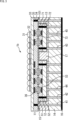
- FIG. 1 is a diagram illustrating a configuration example of an imaging device to which the present technology is applied in a first embodiment.
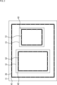
- FIG. 2 is a diagram illustrating an example of a planar configuration of an imaging device.
- FIG. 13 is a diagram illustrating a configuration example of an imaging device to which the present technology is applied in a second embodiment.
- FIG. 2 is a diagram illustrating an example of a planar configuration of an imaging device.
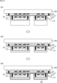
- 1A to 1C are diagrams for explaining a manufacturing process of the imaging device.
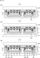
- 1A to 1C are diagrams for explaining a manufacturing process of the imaging device.
- 1A to 1C are diagrams for explaining a manufacturing process of the imaging device.
- 1A to 1C are diagrams for explaining a manufacturing process of the imaging device.
- 1A to 1C are diagrams for explaining a manufacturing process of the imaging device.
- 1A to 1C are diagrams for explaining a manufacturing process of the imaging device.
- 1A to 1C are diagrams for explaining a manufacturing process of the
- First Embodiment 1 is a diagram showing an example of a cross-sectional configuration of an imaging device 1a according to a first embodiment.
- a second semiconductor substrate 12 and a third semiconductor substrate 13 are stacked on the same plane as a first semiconductor substrate 11.
- a support substrate 14 is stacked on the surface of the second semiconductor substrate 12 and the third semiconductor substrate 13 opposite to the surface on which the first semiconductor substrate is stacked.
- the first semiconductor substrate 11 is configured such that an on-chip lens 31, a color filter 32, and an image sensor 33 are stacked in this order, with a wiring layer 34 stacked below the image sensor 33.
- the wiring layer 34 has connection terminals 36 formed thereon for connection to the second semiconductor substrate 12 and the third semiconductor substrate 13, respectively.
- the second semiconductor substrate 12 is a chip stacked on the first semiconductor substrate 11, and is, for example, a memory or logic circuit.
- the second semiconductor substrate 12 is configured to include a wiring layer 51 including a connection terminal 53.
- the connection terminal 36 of the first semiconductor substrate 11 and the connection terminal 53 of the second semiconductor substrate 12 are formed in an exposed state when in the state of a chip before being stacked, and are configured to be directly connected.
- the first semiconductor substrate 11 and the second semiconductor substrate 12 are electrically connected by connecting the connection terminal 36 of the first semiconductor substrate 11 and the connection terminal 53 of the second semiconductor substrate 12.
- the third semiconductor substrate 13 is a chip stacked on the first semiconductor substrate 11, and is, for example, a memory or logic circuit.
- the third semiconductor substrate 13 is configured to include a wiring layer 51 including a connection terminal 73.
- the connection terminal 36 of the first semiconductor substrate 11 and the connection terminal 73 of the third semiconductor substrate 13 are formed in an exposed state when in the chip state during stacking, and are configured to be directly connected.
- the first semiconductor substrate 11 and the third semiconductor substrate 13 are electrically connected by connecting the connection terminal 36 of the first semiconductor substrate 11 and the connection terminal 73 of the third semiconductor substrate 13.
- the first semiconductor substrate 11 and the second semiconductor substrate 12, and the first semiconductor substrate 11 and the third semiconductor substrate 13 are bonded by a bonding film 15.
- the second semiconductor substrate 12, the third semiconductor substrate 13, and the support substrate 14 are bonded by an insulating film 17.
- the second semiconductor substrate 12 and the third semiconductor substrate 13 are configured in a state where they are enclosed within the insulating film 17.
- the bonding film 15 and the insulating film 17 can be oxide films.
- a guard ring 35 is formed on the first semiconductor substrate 11, a guard ring 52 is formed on the second semiconductor substrate 12, and a guard ring 72 is formed on the third semiconductor substrate 13.
- Guard ring 35 is provided to protect elements in first semiconductor substrate 11 when first semiconductor substrate 11 is singulated from the wafer.
- Guard ring 52 is provided to protect elements in second semiconductor substrate 12 when second semiconductor substrate 12 is singulated from the wafer.
- Guard ring 72 is provided to protect elements in third semiconductor substrate 13 when third semiconductor substrate 13 is singulated from the wafer.
- the guard rings are provided in the semiconductor substrate (chip) and are electrically connected to GND (ground) within the chip.
- a through hole 41 is connected to the guard ring 35 of the first semiconductor substrate 11.
- a through hole 42 is connected to the guard ring 52 of the second semiconductor substrate 12.
- a through hole 43 is connected to the guard ring 52 of the third semiconductor substrate 13.
- FIG. 2 shows an example of the planar configuration of the imaging device 1a, illustrating the guard ring 35, guard ring 52, guard ring 72, through hole 41, through hole 42, and through hole 43.
- the guard ring 35 is provided on the outer periphery surrounding an element provided on the first semiconductor substrate 11, for example, the imaging element 33.
- a number of through holes 41 are connected to the guard ring 35.
- Guard ring 52 is provided on the outer periphery surrounding the elements provided on second semiconductor substrate 12. Multiple through holes 42 are connected to guard ring 52.
- Guard ring 72 is provided on the outer periphery surrounding the elements provided on third semiconductor substrate 13. Multiple through holes 43 are connected to guard ring 72.
- the through holes 41 to 43 are arranged at equal intervals. Although an example in which the through holes 41 to 43 are arranged at equal intervals has been shown, they may be arranged at non-equidistant intervals. Although the through holes 41 to 43 are shown as being circular, they may be of a shape other than circular, such as a rectangle. Furthermore, they may be provided with the same size, position, and shape as the guard ring, in other words, they may be provided in a state in which the guard ring and the through holes overlap in a plan view.
- Through holes 41 to 43 have a heat dissipation function.
- a guard ring exists within the semiconductor substrate (chip), and this is electrically connected to GND within the chip. Therefore, heat generated in the semiconductor substrate is efficiently transferred to the guard ring.
- the through holes are connected to such a guard ring.
- heat generated in the first semiconductor substrate 11 is transferred to the through-hole 41 via the guard ring 35.
- the through-hole 41 is connected to the heat dissipation film 16 formed on the bottom surface of the support substrate 14, and the heat transferred to the through-hole 41 is transferred to the heat dissipation film 16 and dissipated to the outside.
- Heat generated in the second semiconductor substrate 12 is transferred to the through hole 42 via the guard ring 52.
- the heat transferred to the through hole 42 is transferred to the heat dissipation film 16 and dissipated to the outside.
- Heat generated in the third semiconductor substrate 13 is transferred to the through hole 43 via the guard ring 72.
- the heat transferred to the through hole 43 is transferred to the heat dissipation film 16 and dissipated to the outside.
- the heat dissipation film 16 is formed as a solid film on the support substrate 14, and is configured to have as large an area as possible.
- the heat dissipation film 16 is formed using a material with high heat dissipation properties, such as metal.
- the heat dissipation film 16 may be used as the GND of the mounting substrate, and may be configured to be electrically connected to the mounting substrate.
- the through holes 42 can be structured to be filled with a material with high thermal conductivity to improve heat dissipation performance.
- the bonding film 15 that bonds the first semiconductor substrate 11 and the second semiconductor substrate 12 can be an insulating film made of a material with good heat dissipation properties.
- Al2O3 can be used as the material for the bonding film 15.
- the imaging device 1a described with reference to Figures 1 and 2, by providing through holes 41, 42, and 43 connected to the guard rings 35, 52, and 72, the heat generated in each of the first semiconductor substrate 11, the second semiconductor substrate 12, and the third semiconductor substrate 13 can be efficiently dissipated.
- FIG. 3 is a diagram showing a cross-sectional configuration example of an imaging device 1b according to the second embodiment
- Fig. 4 is a diagram showing a planar configuration example.
- the same parts as those in the imaging device 1a according to the first embodiment shown in Figs. 1 and 2 are denoted by the same reference numerals, and their description will be omitted as appropriate.
- the imaging device 1b shown in FIG. 3 is configured with a protective film 101, and differs from the imaging device 1a shown in FIG. 1 in that it has additional through holes 44 and 45 connected to the protective film 101, but is otherwise similar.
- the protective film 101 is made of a heat dissipating material, such as a metal.
- the protective film 101 is formed in the region where the first semiconductor substrate 11 and the second semiconductor substrate 12 are not in contact, and in the region where the first semiconductor substrate 11 and the third semiconductor substrate 13 are not in contact.
- the protective film 101 is also formed on the side surface of the second semiconductor substrate 12 and on the surface opposite to the surface in contact with the first semiconductor substrate 11 (referred to as the back surface).
- the protective film 101 is also formed on the side surface of the third semiconductor substrate 13 and on the surface opposite to the surface in contact with the first semiconductor substrate 11 (referred to as the back surface).
- the protective film 101 is formed over the entire surface of the imaging device 1 in a planar view.
- the through holes 44 are arranged at equal intervals within the region where the second semiconductor substrate 12 is located.
- the through holes 45 are arranged at equal intervals within the region where the third semiconductor substrate 13 is located. If there are areas where through holes can be arranged between the guard ring 35 of the first semiconductor substrate 11 and the second semiconductor substrate 12, between the second semiconductor substrate 12 and the third semiconductor substrate 13, and between the guard ring 35 of the first semiconductor substrate 11 and the third semiconductor substrate 13, the through holes may also be arranged there.
- one side of the through hole 44 is connected to the protective film 101 formed on the surface of the second semiconductor substrate 12, and the other side is connected to the heat dissipation film 16. Heat generated in the second semiconductor substrate 12 is transferred from the protective film 101 to the through hole 44, and from the through hole 44 to the heat dissipation film 16, where it is dissipated to the outside.
- the guard ring 52 of the second semiconductor substrate 12 is connected to the through hole 42, so heat also flows from this guard ring 52 to the through hole 42 and from the through hole 42 to the heat dissipation film 16, making it possible to dissipate heat generated in the second semiconductor substrate 12.
- FIG. 3 a structure in which the guard ring 52 and the through hole 42 are directly connected is described as an example, but a configuration in which the guard ring 52 and the through hole 42 are connected with a protective film 101 between them is also possible.
- One side of the through hole 45 is connected to the protective film 101 formed on the surface of the third semiconductor substrate 13, and the other side is connected to the heat dissipation film 16. Heat generated in the third semiconductor substrate 13 is transferred from the protective film 101 to the through hole 45, and from the through hole 45 to the heat dissipation film 16, where it is dissipated to the outside.
- the guard ring 72 of the third semiconductor substrate 13 is connected to the through hole 43, so that heat also flows from the guard ring 72 to the through hole 43 and from the through hole 43 to the heat dissipation film 16, allowing the heat generated in the third semiconductor substrate 13 to be dissipated.
- a structure in which the guard ring 72 and the through hole 43 are directly connected has been described as an example, but a configuration in which the guard ring 72 and the through hole 43 are connected with a protective film 101 between them is also possible.
- Heat generated in the first semiconductor substrate 11 is transferred via the bonding film 15 to the protective film 101 laminated on the bonding film 15. Because the through holes 41 to 45 are connected to the protective film 101, the heat transferred to the protective film 101 is transferred to the through holes 41 to 45, and then transferred from the through holes 41 to 45 to the heat dissipation film 16, and is dissipated to the outside.
- the guard ring 35 of the first semiconductor substrate 11 is connected to the through hole 41, so heat also flows from the guard ring 35 to the through hole 41 and from the through hole 41 to the heat dissipation film 16, allowing heat generated in the first semiconductor substrate 11 to be dissipated.
- FIG. 3 a structure in which the guard ring 35 and the through hole 41 are directly connected is described as an example, but a configuration in which the guard ring 35 and the through hole 41 are connected with a protective film 101 between them is also possible.
- through-holes 44 and 45 are shown as penetrating protective film 101 and contacting second semiconductor substrate 12 or third semiconductor substrate 13, but they may be configured to contact protective film 101 without penetrating protective film 101.
- the heat generated in each of the first semiconductor substrate 11, the second semiconductor substrate 12, and the third semiconductor substrate 13 can be efficiently dissipated.
- FIG. 5 is a diagram for explaining a CoW (Chip on Wafer) technique applied when manufacturing the imaging device 1. As shown in FIG.
- a second semiconductor substrate 12 and a third semiconductor substrate 13 corresponding to memory circuits and logic circuits that have been singulated and confirmed to be good chips are stacked on a wafer 201 corresponding to a first semiconductor substrate 11 on which multiple imaging elements (CMOS (Complementary Metal Oxide Semiconductor) image sensors and CCD (Charge Coupled Device)) are formed.
- CMOS Complementary Metal Oxide Semiconductor
- CCD Charge Coupled Device
- Wafer 201 is a plurality of first semiconductor substrates 11 on which imaging elements 33 are formed by a semiconductor process.
- a plurality of second semiconductor substrates 12 that have been formed on wafer 203 by a semiconductor process, diced, and then electrically inspected to be confirmed as good chips
- a plurality of third semiconductor substrates 13 that have been formed on wafer 204 by a semiconductor process, diced, and then electrically inspected to be confirmed as good chips are selected and rearranged.
- wafers 201, 203, and 204 are manufactured as shown in Figure 5, and the individualized second semiconductor substrate 12 and third semiconductor substrate 13 are stacked on the first semiconductor substrate 11 to manufacture the imaging device 1b.
- connection terminals 36 of the first semiconductor substrate 11 of the wafer 201 are aligned to the connection terminals 53 of the second semiconductor substrate 12 that has been singulated from the wafer 203 and confirmed to be good chips.
- the connection terminals 36 of the first semiconductor substrate 11 of the wafer 201 are aligned to the connection terminals 73 of the third semiconductor substrate 13 that has been singulated from the wafer 204 and confirmed to be good chips.
- Connection terminal 36 and connection terminal 53, and connection terminal 36 and connection terminal 73 are connected, for example, by CuCu bonding. Through this process, first semiconductor substrate 11, second semiconductor substrate 12, and third semiconductor substrate 13 are electrically connected.
- a bonding film 15 made of a heat dissipating material is formed on the first semiconductor substrate 11, and the first semiconductor substrate 11 is bonded to the second semiconductor substrate 12 and the third semiconductor substrate 13.
- step S12 the second semiconductor substrate 12 and the third semiconductor substrate 13 are each thinned, for example, by etching.
- step S13 the guard ring is engraved.
- a via 301 is formed in the guard ring 52 of the second semiconductor substrate 12.
- a via 302 is formed in the guard ring 72 of the third semiconductor substrate 13.
- protective film 101 is formed. If a material that is electrically conductive and has a high thermal conductivity is used as the material for protective film 101, it may be possible to fill vias 301 and 302 when protective film 101 is formed, so that parts of through holes 42 and 43 are formed. If vias 301 and 302 are filled with the same material as protective film 101 in this way, through holes 42 and 43 are formed in a position that contacts protective film 101 without penetrating protective film 101 in a later process.
- vias 301 and 302 are filled with a highly conductive material, and after filling is completed, protective film 101 is formed.
- the material for protective film 101 and the material in vias 301 and 302 are different materials.
- through holes 42 and 43 are formed in positions that penetrate protective film 101 and contact guard rings 52 and 72 through vias 301 and 302.
- step S15 the embedding is performed.
- the insulating film 17 is formed, so that the second semiconductor substrate 12 and the third semiconductor substrate 13 are enclosed within the insulating film 17.
- step S16 the support substrate 14 is attached onto the deposited insulating film 17.
- step S17 vias 311 to 315 that will become the through holes 41 to 45 are formed.
- step S18 ( Figure 8) a material with high heat dissipation properties is filled into vias 311 to 315 to form through holes S41 to S45.
- the through holes 41 to 43 connected to the guard ring and the through holes 44 and 45 connected to the protective film 101 instead of the guard ring may be filled with different materials.
- the through holes 41 to 43 connected to the guard ring may be filled with a material that has heat dissipation properties and electrical conductivity, and the through holes 44 and 45 connected to the protective film 101 may be filled with a material that has high heat dissipation properties.
- step S18 after the through holes 41 to S45 are formed, the heat dissipation film 16 is also formed on the support substrate 14.
- step S18 the wafer 201 is peeled off.
- step S19 the on-chip lens 31 and color filter 32 are provided on the image sensor 33, and the image sensor 1 is completed by being singulated.
- the protective film 101 and the through holes 41 to 45 are formed, and an imaging device 1 with improved heat dissipation is manufactured.
- a second manufacturing process another manufacturing process (hereinafter referred to as a second manufacturing process) until the imaging device 1b shown in FIG. 3 is manufactured by arranging the individualized second semiconductor substrate 12 and third semiconductor substrate 13 on the wafer 201 (first semiconductor substrate 11) as shown in FIG. 5 will be described.
- step S51 the second semiconductor substrate 12 and the third semiconductor substrate 13 are each placed on the wafer 201, and in step S52, the second semiconductor substrate 12 and the third semiconductor substrate 13 are each thinned.
- Steps S51 and S52 are the same as steps S11 and S12 in FIG. 6.
- step S53 protective film 101 is formed.
- Step S53 is basically the same as step S14 (FIG. 6), but differs in that the step of filling vias 301 and 302 with material is omitted because vias 301 and 302 are not formed.
- step S54 the embedding is performed.
- step S55 the support substrate 14 is affixed onto the deposited insulating film 17. Steps S54 and S55 are similar to steps S15 and S16 (FIG. 7).
- step S56 vias 331 to 335 that will become through holes 41 to 45 are formed.
- Step S56 is basically the same as step S17 (FIG. 7) in which vias 311 to 315 are formed, but the positions that are dug are different. Because vias corresponding to vias 301 and 302 have not been formed, in step S56, vias are dug to the positions that correspond to vias 301 and 302. That is, via 332 is dug in one go to the position where it contacts guard ring 52, and via 334 is dug in one go to the position where it contacts guard ring 72.
- step S56 vias 331 to 335 are formed, and then steps S18 to S20 (FIG. 8) are performed to manufacture the imaging device 1.
- the protective film 101 and the through holes 41 to 45 are formed, and an imaging device 1 with improved heat dissipation is manufactured.
- the present technology is applicable to electronic devices in general that use an imaging element in an image capture unit (photoelectric conversion unit), such as imaging devices such as digital still cameras and video cameras, portable terminal devices with imaging functions, copiers that use an imaging element in an image reading unit, etc.
- the imaging element may be in a form formed as a single chip, or in a form of a module having an imaging function in which the imaging unit and a signal processing unit or an optical system are packaged together.
- FIG. 11 is a block diagram showing an example of the configuration of an imaging device as an electronic device to which this technology is applied.
- the image sensor 1000 in FIG. 11 comprises an optical section 1001 consisting of a group of lenses etc., an image sensor (imaging device) 1002, and a DSP (Digital Signal Processor) circuit 1003 which is a camera signal processing circuit.
- the image sensor 1000 also comprises a frame memory 1004, a display section 1005, a recording section 1006, an operation section 1007, and a power supply section 1008.
- the DSP circuit 1003, frame memory 1004, display section 1005, recording section 1006, operation section 1007, and power supply section 1008 are interconnected via a bus line 1009.
- the optical unit 1001 takes in incident light (image light) from a subject and forms an image on the imaging surface of the image sensor 1002.
- the image sensor 1002 converts the amount of incident light formed on the imaging surface by the optical unit 1001 into an electrical signal on a pixel-by-pixel basis and outputs it as a pixel signal.
- the display unit 1005 is composed of a thin display such as an LCD (Liquid Crystal Display) or an organic EL (Electro Luminescence) display, and displays moving images or still images captured by the image sensor 1002.
- the recording unit 1006 records the moving images or still images captured by the image sensor 1002 on a recording medium such as a hard disk or semiconductor memory.
- the operation unit 1007 issues operation commands for the various functions of the image sensor 1000 under the operation of a user.
- the power supply unit 1008 appropriately supplies various types of power to these devices as operating power sources for the DSP circuit 1003, frame memory 1004, display unit 1005, recording unit 1006, and operation unit 1007.
- the imaging device 1 in the first and second embodiments can be applied to a part of the imaging device shown in FIG. 11.
- a system refers to an entire device that is made up of multiple devices.
- a first semiconductor substrate including an image sensor; a second semiconductor substrate laminated on the first semiconductor substrate; a first guard ring included in the first semiconductor substrate; a second guard ring included in the second semiconductor substrate; a support substrate laminated on the second semiconductor substrate; a heat dissipation film laminated on the support substrate and made of a material with high heat dissipation properties; a first through hole, one end of which is connected to the first guard ring and the other end of which is connected to the heat dissipation film, penetrating the support substrate; a second through hole, one end of which is connected to the second guard ring and the other end of which is connected to the heat dissipation film, penetrating the support substrate; and a processing unit that processes a signal from the imaging device.
- 1 imaging device 11 first semiconductor substrate, 12 second semiconductor substrate, 13 third semiconductor substrate, 14 support substrate, 15 bonding film, 16 heat dissipation film, 17 insulating film, 31 on-chip lens, 32 color filter, 33 imaging element, 34 wiring layer, 35 guard ring, 36 connection terminal, 41, 42, 43, 44, 45 through hole, 51 wiring layer, 52 guard ring, 53 connection terminal, 72 guard ring, 73 connection terminal, 101 protective film, 201, 203, 204 wafer, 301, 302, 311 to 315, 331 to 335 vias
Landscapes
- Solid State Image Pick-Up Elements (AREA)
- Internal Circuitry In Semiconductor Integrated Circuit Devices (AREA)
Abstract
Description
図1は、第1の実施の形態における撮像装置1aの断面構成例を示す図である。撮像装置1aは、第1の半導体基板11の同一平面上に、第2の半導体基板12と第3の半導体基板13が積層されている。第2の半導体基板12と第3の半導体基板13の第1の半導体基板が積層されている面とは逆側の面には、支持基板14が積層されている。
図3は、第2の実施の形態における撮像装置1bの断面構成例を示す図であり、図4は、平面構成例を示す図である。図3,4に示した第2の実施の形態における撮像装置1bにおいて、図1,2に示した第1の実施の形態における撮像装置1aと同一の部分には同一の符号を付し、その説明は適宜省略する。
図5は、撮像装置1を製造する際に適用されるCoW(Chip on Wafer)技術について説明するための図である。
図9,10を参照し、図5のようにウェハ201(第1の半導体基板11)上に、個片化された第2の半導体基板12と第3の半導体基板13がそれぞれ配置されることで、図3に示した撮像装置1bが製造されるまでの他の製造工程(第2の製造工程とする)について説明する。
本技術は、デジタルスチルカメラやビデオカメラ等の撮像装置や、撮像機能を有する携帯端末装置や、画像読取部に撮像素子を用いる複写機など、画像取込部(光電変換部)に撮像素子を用いる電子機器全般に対して適用可能である。撮像素子は、ワンチップとして形成された形態であってもよいし、撮像部と信号処理部または光学系とがまとめてパッケージングされた撮像機能を有するモジュール状の形態であってもよい。
(1)
撮像素子を含む第1の半導体基板と、
前記第1の半導体基板に積層されている第2の半導体基板と、
前記第1の半導体基板に含まれる第1のガードリングと、
前記第2の半導体基板に含まれる第2のガードリングと、
前記第2の半導体基板に積層された支持基板と、
前記支持基板に積層され、放熱性の高い材料で形成されている放熱膜と、
一方が前記第1のガードリングに接続され、他方が前記放熱膜に接続され、前記支持基板を貫通している第1の貫通孔と、
一方が前記第2のガードリングに接続され、他方が前記放熱膜に接続され、前記支持基板を貫通している第2の貫通孔と
を備える撮像装置。
(2)
前記第1の貫通孔と前記第2の貫通孔は、熱伝導率が高い材料が充填されている
前記(1)に記載の撮像装置。
(3)
前記第1の半導体基板と前記支持基板の間と、前記第2の半導体基板と前記支持基板との間に成膜された保護膜と、
一方が前記保護膜に接続され、他方が前記放熱膜に接続され、前記支持基板を貫通している第3の貫通孔と
をさらに備える
前記(1)または(2)に記載の撮像装置。
(4)
前記第1のガードリングと前記第1の貫通孔は、前記保護膜を介して接続され、
前記第2のガードリングと前記第2の貫通孔は、前記保護膜を介して接続されている
前記(3)に記載の撮像装置。
(5)
前記放熱膜は、接地されている
前記(1)乃至(4)のいずれかに記載の撮像装置。
(6)
撮像素子を含む第1の半導体基板と、
前記第1の半導体基板に積層されている第2の半導体基板と、
前記第1の半導体基板に含まれる第1のガードリングと、
前記第2の半導体基板に含まれる第2のガードリングと、
前記第2の半導体基板に積層された支持基板と、
前記支持基板に積層され、放熱性の高い材料で形成されている放熱膜と、
一方が前記第1のガードリングに接続され、他方が前記放熱膜に接続され、前記支持基板を貫通している第1の貫通孔と、
一方が前記第2のガードリングに接続され、他方が前記放熱膜に接続され、前記支持基板を貫通している第2の貫通孔と
を備える撮像装置と、
前記撮像装置からの信号を処理する処理部と
を備える電子機器。
Claims (6)
- 撮像素子を含む第1の半導体基板と、
前記第1の半導体基板に積層されている第2の半導体基板と、
前記第1の半導体基板に含まれる第1のガードリングと、
前記第2の半導体基板に含まれる第2のガードリングと、
前記第2の半導体基板に積層された支持基板と、
前記支持基板に積層され、放熱性の高い材料で形成されている放熱膜と、
一方が前記第1のガードリングに接続され、他方が前記放熱膜に接続され、前記支持基板を貫通している第1の貫通孔と、
一方が前記第2のガードリングに接続され、他方が前記放熱膜に接続され、前記支持基板を貫通している第2の貫通孔と
を備える撮像装置。 - 前記第1の貫通孔と前記第2の貫通孔は、熱伝導率が高い材料が充填されている
請求項1に記載の撮像装置。 - 前記第1の半導体基板と前記支持基板の間と、前記第2の半導体基板と前記支持基板との間に成膜された保護膜と、
一方が前記保護膜に接続され、他方が前記放熱膜に接続され、前記支持基板を貫通している第3の貫通孔と
をさらに備える
請求項1に記載の撮像装置。 - 前記第1のガードリングと前記第1の貫通孔は、前記保護膜を介して接続され、
前記第2のガードリングと前記第2の貫通孔は、前記保護膜を介して接続されている
請求項3に記載の撮像装置。 - 前記放熱膜は、接地されている
請求項1に記載の撮像装置。 - 撮像素子を含む第1の半導体基板と、
前記第1の半導体基板に積層されている第2の半導体基板と、
前記第1の半導体基板に含まれる第1のガードリングと、
前記第2の半導体基板に含まれる第2のガードリングと、
前記第2の半導体基板に積層された支持基板と、
前記支持基板に積層され、放熱性の高い材料で形成されている放熱膜と、
一方が前記第1のガードリングに接続され、他方が前記放熱膜に接続され、前記支持基板を貫通している第1の貫通孔と、
一方が前記第2のガードリングに接続され、他方が前記放熱膜に接続され、前記支持基板を貫通している第2の貫通孔と
を備える撮像装置と、
前記撮像装置からの信号を処理する処理部と
を備える電子機器。
Priority Applications (2)
| Application Number | Priority Date | Filing Date | Title |
|---|---|---|---|
| CN202380086379.XA CN120435930A (zh) | 2023-01-11 | 2023-12-27 | 摄像装置和电子设备 |
| KR1020257024627A KR20250133688A (ko) | 2023-01-11 | 2023-12-27 | 촬상 장치, 전자 기기 |
Applications Claiming Priority (2)
| Application Number | Priority Date | Filing Date | Title |
|---|---|---|---|
| JP2023-002086 | 2023-01-11 | ||
| JP2023002086A JP2024098542A (ja) | 2023-01-11 | 2023-01-11 | 撮像装置、電子機器 |
Publications (1)
| Publication Number | Publication Date |
|---|---|
| WO2024150679A1 true WO2024150679A1 (ja) | 2024-07-18 |
Family
ID=91896988
Family Applications (1)
| Application Number | Title | Priority Date | Filing Date |
|---|---|---|---|
| PCT/JP2023/046883 Ceased WO2024150679A1 (ja) | 2023-01-11 | 2023-12-27 | 撮像装置、電子機器 |
Country Status (4)
| Country | Link |
|---|---|
| JP (1) | JP2024098542A (ja) |
| KR (1) | KR20250133688A (ja) |
| CN (1) | CN120435930A (ja) |
| WO (1) | WO2024150679A1 (ja) |
Citations (3)
| Publication number | Priority date | Publication date | Assignee | Title |
|---|---|---|---|---|
| WO2016185883A1 (ja) * | 2015-05-18 | 2016-11-24 | ソニー株式会社 | 半導体装置および撮像装置 |
| JP2018006507A (ja) * | 2016-06-30 | 2018-01-11 | 株式会社デンソー | 半導体装置およびその製造方法 |
| WO2022154077A1 (ja) * | 2021-01-15 | 2022-07-21 | 株式会社村田製作所 | 半導体装置及び半導体モジュール |
Family Cites Families (6)
| Publication number | Priority date | Publication date | Assignee | Title |
|---|---|---|---|---|
| JP2015076502A (ja) | 2013-10-09 | 2015-04-20 | ソニー株式会社 | 半導体装置およびその製造方法、並びに電子機器 |
| JP6729044B2 (ja) | 2016-06-20 | 2020-07-22 | 大日本印刷株式会社 | 配線基板およびその製造方法、ならびに半導体装置の製造方法 |
| JP2018116972A (ja) | 2017-01-16 | 2018-07-26 | 富士通株式会社 | 電子回路装置及び電子回路装置の製造方法 |
| JP6443494B2 (ja) | 2017-05-25 | 2018-12-26 | 株式会社ニコン | 撮像ユニット及び撮像装置 |
| TWI905469B (zh) | 2017-10-30 | 2025-11-21 | 日商索尼半導體解決方案公司 | 固體攝像裝置及電子機器 |
| JP2020191339A (ja) | 2019-05-20 | 2020-11-26 | ソニーセミコンダクタソリューションズ株式会社 | 半導体装置及び電子機器 |
-
2023
- 2023-01-11 JP JP2023002086A patent/JP2024098542A/ja active Pending
- 2023-12-27 CN CN202380086379.XA patent/CN120435930A/zh active Pending
- 2023-12-27 WO PCT/JP2023/046883 patent/WO2024150679A1/ja not_active Ceased
- 2023-12-27 KR KR1020257024627A patent/KR20250133688A/ko active Pending
Patent Citations (3)
| Publication number | Priority date | Publication date | Assignee | Title |
|---|---|---|---|---|
| WO2016185883A1 (ja) * | 2015-05-18 | 2016-11-24 | ソニー株式会社 | 半導体装置および撮像装置 |
| JP2018006507A (ja) * | 2016-06-30 | 2018-01-11 | 株式会社デンソー | 半導体装置およびその製造方法 |
| WO2022154077A1 (ja) * | 2021-01-15 | 2022-07-21 | 株式会社村田製作所 | 半導体装置及び半導体モジュール |
Also Published As
| Publication number | Publication date |
|---|---|
| JP2024098542A (ja) | 2024-07-24 |
| KR20250133688A (ko) | 2025-09-08 |
| CN120435930A (zh) | 2025-08-05 |
Similar Documents
| Publication | Publication Date | Title |
|---|---|---|
| JP5794002B2 (ja) | 固体撮像装置、電子機器 | |
| US9373653B2 (en) | Stepped package for image sensor | |
| TWI253149B (en) | Semiconductor device, module for optical devices, and manufacturing method of semiconductor device | |
| CN1622334B (zh) | 固态成像装置及其制造方法 | |
| CN107039480B (zh) | 固体摄像器件和电子装置 | |
| US7923798B2 (en) | Optical device and method for fabricating the same, camera module using optical device, and electronic equipment mounting camera module | |
| US8902356B2 (en) | Image sensor module having image sensor package | |
| US11043436B2 (en) | Semiconductor device, manufacturing method, imaging device, and electronic apparatus for enabling component mounting with high flatness | |
| US20090283311A1 (en) | Electronic element wafer module and method for manufacturing electronic element wafer module, electronic element module, and electronic information device | |
| US10446598B2 (en) | Semiconductor device, manufacturing method, and electronic apparatus | |
| US20100315546A1 (en) | Imaging Device and Manufacturing method therefor | |
| TW200830870A (en) | Package module and electronic assembly for image sensor device and fabrication method thereof | |
| JP7158846B2 (ja) | 半導体装置および機器 | |
| TWI800487B (zh) | 固體攝像元件及製造方法、以及電子機器 | |
| JP2016033963A (ja) | 半導体パッケージ及びその製造方法、並びに撮像装置 | |
| CN102376731A (zh) | 图像拾取模块和照相机 | |
| JP2009290033A (ja) | 電子素子ウェハモジュールおよびその製造方法、電子素子モジュール、電子情報機器 | |
| WO2020039733A1 (ja) | 半導体装置、電子機器、および半導体装置の製造方法 | |
| JP2010050260A (ja) | 半導体イメージセンサ | |
| JP2007027713A (ja) | 透明カバーが付着されている光学装置の製造方法及びそれを利用した光学装置モジュールの製造方法 | |
| JP7389029B2 (ja) | 固体撮像装置、電子機器、および固体撮像装置の製造方法 | |
| WO2024150679A1 (ja) | 撮像装置、電子機器 | |
| US11393862B2 (en) | Manufacture of semiconductor module with dual molding | |
| JP2022189647A (ja) | 固体撮像装置および電子機器 | |
| CN100459140C (zh) | 固态成像器件及其制造方法和照相机模块 |
Legal Events
| Date | Code | Title | Description |
|---|---|---|---|
| 121 | Ep: the epo has been informed by wipo that ep was designated in this application |
Ref document number: 23916292 Country of ref document: EP Kind code of ref document: A1 |
|
| WWE | Wipo information: entry into national phase |
Ref document number: 202380086379.X Country of ref document: CN |
|
| ENP | Entry into the national phase |
Ref document number: 1020257024627 Country of ref document: KR Free format text: ST27 STATUS EVENT CODE: A-0-1-A10-A15-NAP-PA0105 (AS PROVIDED BY THE NATIONAL OFFICE) |
|
| WWP | Wipo information: published in national office |
Ref document number: 202380086379.X Country of ref document: CN |
|
| NENP | Non-entry into the national phase |
Ref country code: DE |
|
| 122 | Ep: pct application non-entry in european phase |
Ref document number: 23916292 Country of ref document: EP Kind code of ref document: A1 |