WO2024150428A1 - AlN単結晶基板およびデバイス - Google Patents
AlN単結晶基板およびデバイス Download PDFInfo
- Publication number
- WO2024150428A1 WO2024150428A1 PCT/JP2023/000869 JP2023000869W WO2024150428A1 WO 2024150428 A1 WO2024150428 A1 WO 2024150428A1 JP 2023000869 W JP2023000869 W JP 2023000869W WO 2024150428 A1 WO2024150428 A1 WO 2024150428A1
- Authority
- WO
- WIPO (PCT)
- Prior art keywords
- concentration
- single crystal
- carbon
- boron
- aln single
- Prior art date
- Legal status (The legal status is an assumption and is not a legal conclusion. Google has not performed a legal analysis and makes no representation as to the accuracy of the status listed.)
- Ceased
Links
Images

Classifications
-
- C—CHEMISTRY; METALLURGY
- C01—INORGANIC CHEMISTRY
- C01B—NON-METALLIC ELEMENTS; COMPOUNDS THEREOF; METALLOIDS OR COMPOUNDS THEREOF NOT COVERED BY SUBCLASS C01C
- C01B21/00—Nitrogen; Compounds thereof
- C01B21/06—Binary compounds of nitrogen with metals, with silicon, or with boron, or with carbon, i.e. nitrides; Compounds of nitrogen with more than one metal, silicon or boron
- C01B21/072—Binary compounds of nitrogen with metals, with silicon, or with boron, or with carbon, i.e. nitrides; Compounds of nitrogen with more than one metal, silicon or boron with aluminium
-
- C—CHEMISTRY; METALLURGY
- C23—COATING METALLIC MATERIAL; COATING MATERIAL WITH METALLIC MATERIAL; CHEMICAL SURFACE TREATMENT; DIFFUSION TREATMENT OF METALLIC MATERIAL; COATING BY VACUUM EVAPORATION, BY SPUTTERING, BY ION IMPLANTATION OR BY CHEMICAL VAPOUR DEPOSITION, IN GENERAL; INHIBITING CORROSION OF METALLIC MATERIAL OR INCRUSTATION IN GENERAL
- C23C—COATING METALLIC MATERIAL; COATING MATERIAL WITH METALLIC MATERIAL; SURFACE TREATMENT OF METALLIC MATERIAL BY DIFFUSION INTO THE SURFACE, BY CHEMICAL CONVERSION OR SUBSTITUTION; COATING BY VACUUM EVAPORATION, BY SPUTTERING, BY ION IMPLANTATION OR BY CHEMICAL VAPOUR DEPOSITION, IN GENERAL
- C23C16/00—Chemical coating by decomposition of gaseous compounds, without leaving reaction products of surface material in the coating, i.e. chemical vapour deposition [CVD] processes
- C23C16/22—Chemical coating by decomposition of gaseous compounds, without leaving reaction products of surface material in the coating, i.e. chemical vapour deposition [CVD] processes characterised by the deposition of inorganic material, other than metallic material
- C23C16/30—Deposition of compounds, mixtures or solid solutions, e.g. borides, carbides, nitrides
- C23C16/34—Nitrides
-
- C—CHEMISTRY; METALLURGY
- C30—CRYSTAL GROWTH
- C30B—SINGLE-CRYSTAL GROWTH; UNIDIRECTIONAL SOLIDIFICATION OF EUTECTIC MATERIAL OR UNIDIRECTIONAL DEMIXING OF EUTECTOID MATERIAL; REFINING BY ZONE-MELTING OF MATERIAL; PRODUCTION OF A HOMOGENEOUS POLYCRYSTALLINE MATERIAL WITH DEFINED STRUCTURE; SINGLE CRYSTALS OR HOMOGENEOUS POLYCRYSTALLINE MATERIAL WITH DEFINED STRUCTURE; AFTER-TREATMENT OF SINGLE CRYSTALS OR A HOMOGENEOUS POLYCRYSTALLINE MATERIAL WITH DEFINED STRUCTURE; APPARATUS THEREFOR
- C30B25/00—Single-crystal growth by chemical reaction of reactive gases, e.g. chemical vapour-deposition growth
- C30B25/02—Epitaxial-layer growth
- C30B25/18—Epitaxial-layer growth characterised by the substrate
- C30B25/20—Epitaxial-layer growth characterised by the substrate the substrate being of the same materials as the epitaxial layer
-
- C—CHEMISTRY; METALLURGY
- C30—CRYSTAL GROWTH
- C30B—SINGLE-CRYSTAL GROWTH; UNIDIRECTIONAL SOLIDIFICATION OF EUTECTIC MATERIAL OR UNIDIRECTIONAL DEMIXING OF EUTECTOID MATERIAL; REFINING BY ZONE-MELTING OF MATERIAL; PRODUCTION OF A HOMOGENEOUS POLYCRYSTALLINE MATERIAL WITH DEFINED STRUCTURE; SINGLE CRYSTALS OR HOMOGENEOUS POLYCRYSTALLINE MATERIAL WITH DEFINED STRUCTURE; AFTER-TREATMENT OF SINGLE CRYSTALS OR A HOMOGENEOUS POLYCRYSTALLINE MATERIAL WITH DEFINED STRUCTURE; APPARATUS THEREFOR
- C30B29/00—Single crystals or homogeneous polycrystalline material with defined structure characterised by the material or by their shape
- C30B29/10—Inorganic compounds or compositions
- C30B29/38—Nitrides
-
- C—CHEMISTRY; METALLURGY
- C30—CRYSTAL GROWTH
- C30B—SINGLE-CRYSTAL GROWTH; UNIDIRECTIONAL SOLIDIFICATION OF EUTECTIC MATERIAL OR UNIDIRECTIONAL DEMIXING OF EUTECTOID MATERIAL; REFINING BY ZONE-MELTING OF MATERIAL; PRODUCTION OF A HOMOGENEOUS POLYCRYSTALLINE MATERIAL WITH DEFINED STRUCTURE; SINGLE CRYSTALS OR HOMOGENEOUS POLYCRYSTALLINE MATERIAL WITH DEFINED STRUCTURE; AFTER-TREATMENT OF SINGLE CRYSTALS OR A HOMOGENEOUS POLYCRYSTALLINE MATERIAL WITH DEFINED STRUCTURE; APPARATUS THEREFOR
- C30B29/00—Single crystals or homogeneous polycrystalline material with defined structure characterised by the material or by their shape
- C30B29/10—Inorganic compounds or compositions
- C30B29/40—AIIIBV compounds wherein A is B, Al, Ga, In or Tl and B is N, P, As, Sb or Bi
- C30B29/403—AIII-nitrides
-
- H—ELECTRICITY
- H10—SEMICONDUCTOR DEVICES; ELECTRIC SOLID-STATE DEVICES NOT OTHERWISE PROVIDED FOR
- H10H—INORGANIC LIGHT-EMITTING SEMICONDUCTOR DEVICES HAVING POTENTIAL BARRIERS
- H10H20/00—Individual inorganic light-emitting semiconductor devices having potential barriers, e.g. light-emitting diodes [LED]
- H10H20/80—Constructional details
- H10H20/81—Bodies
- H10H20/822—Materials of the light-emitting regions
- H10H20/824—Materials of the light-emitting regions comprising only Group III-V materials, e.g. GaP
- H10H20/825—Materials of the light-emitting regions comprising only Group III-V materials, e.g. GaP containing nitrogen, e.g. GaN
- H10H20/8252—Materials of the light-emitting regions comprising only Group III-V materials, e.g. GaP containing nitrogen, e.g. GaN characterised by the dopants
-
- H—ELECTRICITY
- H10—SEMICONDUCTOR DEVICES; ELECTRIC SOLID-STATE DEVICES NOT OTHERWISE PROVIDED FOR
- H10P—GENERIC PROCESSES OR APPARATUS FOR THE MANUFACTURE OR TREATMENT OF DEVICES COVERED BY CLASS H10
- H10P14/00—Formation of materials, e.g. in the shape of layers or pillars
- H10P14/20—Formation of materials, e.g. in the shape of layers or pillars of semiconductor materials
- H10P14/29—Formation of materials, e.g. in the shape of layers or pillars of semiconductor materials characterised by the substrates
-
- C—CHEMISTRY; METALLURGY
- C01—INORGANIC CHEMISTRY
- C01P—INDEXING SCHEME RELATING TO STRUCTURAL AND PHYSICAL ASPECTS OF SOLID INORGANIC COMPOUNDS
- C01P2002/00—Crystal-structural characteristics
- C01P2002/80—Crystal-structural characteristics defined by measured data other than those specified in group C01P2002/70
- C01P2002/84—Crystal-structural characteristics defined by measured data other than those specified in group C01P2002/70 by UV- or VIS- data
-
- C—CHEMISTRY; METALLURGY
- C01—INORGANIC CHEMISTRY
- C01P—INDEXING SCHEME RELATING TO STRUCTURAL AND PHYSICAL ASPECTS OF SOLID INORGANIC COMPOUNDS
- C01P2006/00—Physical properties of inorganic compounds
- C01P2006/80—Compositional purity
Definitions
- the present invention relates to AlN single crystal substrates and devices.
- the present invention relates to AlN single crystal substrates used to manufacture LEDs (Light Emitting Diodes) that emit light in the ultraviolet range.
- LEDs Light Emitting Diodes
- LEDs that emit light in the ultraviolet range In recent years, there has been a demand for LEDs that emit light in the ultraviolet range. Such LEDs that emit light in the deep ultraviolet range can be used for sterilization and other applications.
- An AlN single crystal substrate is used as the base substrate.
- Patent Document 1 discloses that by substituting some of the Al atoms of an AlN crystal with a group IIIa element (Sc, Y, La, etc.) and/or a group IIIb element (B, Ga, In, etc.) and substituting one adjacent nitrogen (N) atom with an oxygen (O) atom, a shallow impurity level is formed, and a low-resistance n-type AlN crystal can be obtained.
- the total concentration (C 3A ) of the group IIIa element and/or group IIIb element is 1 ⁇ 10 18 cm -3 or more
- the O concentration (C O ) is 0.01C 3A ⁇ C O ⁇ 1.5C 3A .
- Patent Document 2 discloses an aluminum nitride single crystal containing oxygen atoms and carbon atoms, characterized in that the aluminum nitride single crystal satisfies the condition of the formula [O]-[C]>0 when the concentration of oxygen atoms is [O]cm -3 and the concentration of carbon atoms is [C]cm -3 .
- an AlN single crystal substrate When an AlN single crystal substrate is used as an LED that emits light in the ultraviolet region, it is required that the substrate has high transmittance in the ultraviolet region.
- the impurity concentration in the AlN single crystal substrate may be reduced.
- advanced control and special manufacturing equipment are required during single crystal growth to reduce the impurity concentration.
- Such manufacturing equipment is generally expensive, which increases the manufacturing cost of the AlN single crystal substrate. Therefore, there is room for improvement in the method of controlling the impurity concentration to obtain an AlN single crystal substrate with high transmittance in the ultraviolet region.
- An object of the present invention is to provide an AlN single crystal substrate or the like that can achieve high transmittance in the ultraviolet region by adjusting the impurity concentration.
- the present invention provides an AlN single crystal substrate containing carbon and boron as impurities, in which, when the carbon concentration and the boron concentration are expressed as the number of atoms per cm3 , the ratio of the carbon concentration to the boron concentration satisfies 0.22 ⁇ [boron concentration]/[carbon concentration] ⁇ 6.85.
- the present invention also provides an AlN single crystal substrate containing carbon and boron as impurities, with the carbon concentration and the boron concentration being set so that the absorption coefficient for ultraviolet light having a wavelength of 265 nm is less than 60/cm.
- the present invention further provides a device comprising the above-mentioned AlN single crystal substrate.
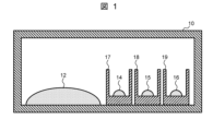
- FIG. 2 is a diagram showing an apparatus used in heat treatment of AlN polycrystalline powder.
- FIG. 2 is a diagram showing a film formation apparatus used in forming an AlN single crystal layer.
- AlN single crystal substrate refers to a substrate made of a single crystal of aluminum nitride (AlN). Note that “single crystal” does not mean that the substrate is entirely made of a single crystal, and may contain, for example, crystal defects.
- the AlN single crystal substrate of the present embodiment contains carbon (C) and boron (B) as impurities.
- C carbon
- B boron
- the ratio of the carbon concentration and the boron concentration is 0.22 ⁇ [boron concentration]/[carbon concentration] ⁇ 6.85. If the [boron concentration]/[carbon concentration] is less than 0.22, the amount of C impurity, which is considered to have absorption in the deep outer region, becomes relatively large, which is undesirable. Also, if the [boron concentration]/[carbon concentration] exceeds 6.85, it is undesirable in that very small pores are easily generated and light is scattered.
- the ratio satisfies 1.17 ⁇ [boron concentration]/[carbon concentration] ⁇ 5.09, and it is even more preferable that the ratio satisfies 1.45 ⁇ [boron concentration]/[carbon concentration] ⁇ 3.33.
- silicon (Si) may be contained as an impurity.
- the ratio of the concentration of carbon to the concentration of silicon may be 0.005 ⁇ [silicon concentration]/[carbon concentration] ⁇ 0.27. It is preferable that this ratio is 0.01 ⁇ [silicon concentration]/[carbon concentration] ⁇ 0.2, and more preferably, this ratio is 0.02 ⁇ [silicon concentration]/[carbon concentration] ⁇ 0.08.
- the transmittance of the AlN single crystal substrate in the ultraviolet region can be improved. In other words, even if impurities are contained, the transmittance of the AlN single crystal substrate in the ultraviolet region can be improved. In addition, the transmittance of the AlN single crystal substrate in the ultraviolet region can be improved without using advanced control and special manufacturing equipment during the single crystal growth of the AlN single crystal substrate. As a result, the manufacturing cost of the AlN single crystal substrate tends to be low.
- the absorption coefficient for ultraviolet light having a wavelength of 265 nm is required to be less than 60/cm. It is even more preferable that the absorption coefficient is less than 50/cm. This absorption coefficient can be measured by the following method.
- the total light transmittance Ta of the AlN single crystal is measured using a spectrophotometer. Using this measured value and the theoretical transmittance Tt of the AlN single crystal, the absorption coefficient ⁇ of the AlN single crystal is calculated using the following formula (I), and then the transmittance T100 ⁇ m converted to 100 ⁇ m is calculated using the following formula (II).
- t is the actual thickness (cm) of the sample.
- the concentrations of carbon, boron and silicon are within the ranges of the following expressions (1) to (3). 3.7 ⁇ 10 18 cm ⁇ 3 ⁇ [carbon concentration] ⁇ 5.0 ⁇ 10 19 cm ⁇ 3 ...(1) 9.4 ⁇ 10 18 cm ⁇ 3 ⁇ [boron concentration] ⁇ 8.4 ⁇ 10 19 cm ⁇ 3 ... (2) 1.0 ⁇ 10 17 cm ⁇ 3 ⁇ [silicon concentration] ⁇ 2.0 ⁇ 10 19 cm ⁇ 3 ... (3) It is more preferable that the concentrations of carbon, boron and silicon are within the ranges of the following expressions (4) to (6).
- the absorption coefficient of the AlN single crystal substrate in the ultraviolet region tends to be small.
- the AlN single crystal substrate in this embodiment is preferably an oriented layer oriented in both the c-axis and a-axis directions, and may contain mosaic crystals.
- Mosaic crystals are a collection of crystals that do not have clear grain boundaries, but whose orientation direction is slightly different from either or both of the c-axis and a-axis.
- Such an oriented layer has a configuration in which the crystal orientation is roughly aligned in the approximately normal direction (c-axis direction) and the in-plane direction (a-axis direction). With this configuration, it is possible to form a semiconductor layer thereon that has excellent quality, particularly excellent orientation. In other words, when a semiconductor layer is formed on the oriented layer, the crystal orientation of the semiconductor layer roughly follows the crystal orientation of the oriented layer. Therefore, it is easy to form a semiconductor film on the AlN single crystal substrate as an oriented film.
- the AlN single crystal substrate of this embodiment can be manufactured by various methods.
- a seed substrate may be prepared and epitaxially grown thereon, or an AlN single crystal substrate may be manufactured directly by spontaneous nucleation without using a seed substrate.
- the seed substrate used may be an AlN substrate so as to achieve homoepitaxial growth, or a substrate other than the seed substrate may be used for heteroepitaxial growth.
- any of the vapor phase film growth method, liquid phase film growth method, and solid phase film growth method may be used for the growth of the single crystal, it is preferable to grow the AlN single crystal by using the vapor phase film growth method, and then grind and remove the seed substrate portion as necessary to obtain the desired AlN single crystal substrate.
- vapor phase film formation method examples include various CVD (chemical vapor deposition) methods (for example, thermal CVD, plasma CVD, MOVPE, etc.), sputtering, hydride vapor phase epitaxy (HVPE), molecular beam epitaxy (MBE), sublimation, pulsed laser deposition (PLD), etc., preferably sublimation or HVPE.
- CVD chemical vapor deposition
- HVPE hydride vapor phase epitaxy
- MBE molecular beam epitaxy
- sublimation pulsed laser deposition
- PLD pulsed laser deposition
- liquid phase film formation method examples include solution growth (for example, flux method), etc.
- AlN single crystal substrate even if the AlN single crystal is not directly formed on the seed substrate, it is also possible to obtain an AlN single crystal substrate by a process of forming an orientation precursor layer, a process of converting the orientation precursor layer into an AlN single crystal layer by heat treatment, and a process of grinding off the seed substrate.
- the method for forming the alignment precursor layer include the AD (aerosol deposition) method and the HPPD (supersonic plasma particle deposition) method.
- a device can also be manufactured using the AlN single crystal substrate of this embodiment. That is, a device preferably equipped with an AlN single crystal substrate is provided. Examples of such devices include deep ultraviolet laser diodes, deep ultraviolet diodes, power electronic devices, high frequency devices, heat sinks, etc.
- the manufacturing method of a device using an AlN single crystal substrate is not particularly limited, and the device can be manufactured by a known method.
- AlN single crystal substrate was produced with the composition shown in Table 1 below. That is, the AlN single crystal substrate was produced so that the concentrations (C amount, B amount, Si amount) of the impurities carbon (C), boron (B), and silicon (Si) were the concentrations shown in Table 1. In addition, at this time, [boron concentration]/[silicon concentration] (Si/C) and [boron concentration]/[carbon concentration] (B/C) are as shown in Table 1. The concentrations (C amount, B amount, Si amount) are rounded off to the second decimal place.
- Si/C and B/C may not be the values shown in Table 1, but Table 1 shows Si/C and B/C calculated at accurate concentrations taking into account the second decimal place and beyond.
- Example 1 an AlN single crystal substrate was fabricated by sublimation deposition.
- the sublimation deposition method used in Example 1 includes the steps of (a) heat treating AlN polycrystalline powder, and (b) forming an AlN single crystal layer.
- FIG. 1 is a diagram showing an apparatus used in the heat treatment of AlN polycrystalline powder.
- Commercially available AlN powder 12 with an average particle size of 1 ⁇ m used as a raw material for AlN single crystals was placed in the BN sheath 10.
- Commercially available graphite powder 14 with an average particle size of 1 ⁇ m was placed in the BN crucible 17 in a ratio of 6 parts by weight per 100 parts by weight of the AlN powder.
- BN powder 15 with an average particle size of 3 ⁇ m was placed in the BN crucible 18 in a ratio of 3 parts by weight per 100 parts by weight of the AlN powder.
- Si 3 N 4 powder 16 with an average particle size of 0.1 ⁇ m was placed in the BN crucible 19 in a ratio of 1 part by weight per 100 parts by weight of the AlN powder.
- These BN crucibles 17 to 19 were placed in the BN sheath 10 so as not to directly touch the AlN powder 12.
- the BN crucibles 17 to 19 are large enough to be stored in the BN sheath 10.
- the BN sheath 10 was heat-treated in a graphite heater furnace in an N2 atmosphere at 0.1 to 10 atm and 2200° C. In this manner, the AlN powder 12, which was AlN polycrystalline powder, was heat-treated to produce AlN raw material powder.
- FIG. 2 is a diagram showing a deposition apparatus 20 used in depositing the AlN single crystal layer.
- the illustrated film formation apparatus 20 includes a heat insulating material 24 for insulating a crucible 22 , which is a crystal growth container, and a coil 26 for heating the crucible 22 .
- the crucible 22 containing the AlN raw material powder 28 produced in (a) above was placed inside the film-forming apparatus 20.
- a SiC substrate was placed as a seed substrate 30 for precipitating a sublimate of the AlN raw material powder 28 at an upper portion inside the film-forming apparatus 20 so as not to come into contact with the crucible 22.
- the crucible 22 was pressurized at 50 kPa in a N2 atmosphere, and the portion in the crucible 22 near the AlN raw material powder was heated to 100°C by high-frequency induction heating using the coil 26. Meanwhile, the portion in the crucible 22 near the SiC substrate was heated to a lower temperature (temperature difference of 200°C) and held at that temperature, thereby re-precipitating the AlN single crystal layer 32 on the SiC substrate. The holding time was 10 hours.
- an AlN single crystal substrate was produced having the composition in which the respective concentrations of carbon (C), boron (B), and silicon (Si) (C amount, B amount, and Si amount) are shown in Table 1.
- the concentration of each element was measured using a dynamic SIMS (Secondary Ion Mass Spectrometry) as a measuring device.
- the measuring device was a CAMECA IMS-7f manufactured by AMETECH Co., Ltd., with a primary ion species of Cs + , a primary acceleration voltage of 15 kV, and a detection area of 20 ⁇ m ⁇ 20 ⁇ m.
- the lower measurement limits of carbon (C), boron (B), and silicon (Si) using this measuring device were all 1.0 ⁇ 10 17 cm ⁇ 3 .
- Examples 2 to 9, Comparative Examples 1 to 3 An AlN single crystal substrate was fabricated in the same manner as in Example 1, except that the amounts of graphite powder 14 , BN powder 15, and Si3N4 powder 16 were changed. As a result, an AlN single crystal substrate was fabricated in which the concentrations of carbon (C), boron (B), and silicon (Si) (C amount, B amount, Si amount) were as shown in Table 1.
- Examples 1 to 9 are cases where carbon (C) and boron (B) are included as impurities, and the ratio of the carbon concentration and the boron concentration (B/C) is 0.22 ⁇ [boron concentration]/[carbon concentration] ⁇ 6.85.
- Examples 2 to 9 are cases where silicon (Si) is further included as an impurity, and the ratio of the carbon concentration and the silicon concentration (Si/C) is 0.005 ⁇ [silicon concentration]/[carbon concentration] ⁇ 0.27. Note that in Example 1, silicon (Si) is below the detection limit as an impurity, and Si/C is calculated to be 0.005, but is shown here as 0.00. In Examples 1 to 9, the absorption coefficient was rated A or B, which was a good result.
- Comparative Example 1 contains carbon (C) and boron (B) as impurities, but the ratio of the carbon concentration to the boron concentration (B/C) is less than 0.22.
- Comparative Example 2 is a case where boron (B) is hardly contained as an impurity. Note that, in calculation, B/C is 0.001, but is shown here as 0.00.
- Comparative Example 3 contains carbon (C) and boron (B) as impurities, but the ratio of the carbon concentration to the boron concentration (B/C) exceeds 6.85. In Comparative Examples 1 to 3, the absorption coefficient was evaluated as C, which was poor.
- Reference Signs List 12 AlN powder, 14: graphite powder, 15: BN powder, 16: Si 3 N 4 powder, 17, 18, 19: BN crucible, 20: film forming apparatus, 28: AlN raw material powder
Landscapes
- Chemical & Material Sciences (AREA)
- Organic Chemistry (AREA)
- Inorganic Chemistry (AREA)
- Engineering & Computer Science (AREA)
- Materials Engineering (AREA)
- Metallurgy (AREA)
- Crystallography & Structural Chemistry (AREA)
- General Chemical & Material Sciences (AREA)
- Chemical Kinetics & Catalysis (AREA)
- Mechanical Engineering (AREA)
- Crystals, And After-Treatments Of Crystals (AREA)
Priority Applications (4)
| Application Number | Priority Date | Filing Date | Title |
|---|---|---|---|
| JP2024569996A JPWO2024150428A1 (https=) | 2023-01-13 | 2023-01-13 | |
| PCT/JP2023/000869 WO2024150428A1 (ja) | 2023-01-13 | 2023-01-13 | AlN単結晶基板およびデバイス |
| TW112145513A TW202428507A (zh) | 2023-01-13 | 2023-11-24 | 氮化鋁單晶基板及裝置 |
| US19/256,242 US20250333877A1 (en) | 2023-01-13 | 2025-07-01 | AlN SINGLE CRYSTAL SUBSTRATE AND DEVICE |
Applications Claiming Priority (1)
| Application Number | Priority Date | Filing Date | Title |
|---|---|---|---|
| PCT/JP2023/000869 WO2024150428A1 (ja) | 2023-01-13 | 2023-01-13 | AlN単結晶基板およびデバイス |
Related Child Applications (1)
| Application Number | Title | Priority Date | Filing Date |
|---|---|---|---|
| US19/256,242 Continuation US20250333877A1 (en) | 2023-01-13 | 2025-07-01 | AlN SINGLE CRYSTAL SUBSTRATE AND DEVICE |
Publications (1)
| Publication Number | Publication Date |
|---|---|
| WO2024150428A1 true WO2024150428A1 (ja) | 2024-07-18 |
Family
ID=91896725
Family Applications (1)
| Application Number | Title | Priority Date | Filing Date |
|---|---|---|---|
| PCT/JP2023/000869 Ceased WO2024150428A1 (ja) | 2023-01-13 | 2023-01-13 | AlN単結晶基板およびデバイス |
Country Status (4)
| Country | Link |
|---|---|
| US (1) | US20250333877A1 (https=) |
| JP (1) | JPWO2024150428A1 (https=) |
| TW (1) | TW202428507A (https=) |
| WO (1) | WO2024150428A1 (https=) |
Citations (4)
| Publication number | Priority date | Publication date | Assignee | Title |
|---|---|---|---|---|
| WO2013094058A1 (ja) * | 2011-12-22 | 2013-06-27 | 国立大学法人東京農工大学 | 窒化アルミニウム単結晶基板、およびこれらの製造方法 |
| JP2014181178A (ja) * | 2013-03-15 | 2014-09-29 | Nitride Solutions Inc | 低炭素iii族窒化物結晶 |
| US20190145020A1 (en) * | 2017-11-10 | 2019-05-16 | Robert T. Bondokov | Thermal control for formation and processing of aluminum nitride |
| WO2021132491A1 (ja) * | 2019-12-24 | 2021-07-01 | 株式会社トクヤマ | Iii族窒化物単結晶基板およびその製造方法 |
-
2023
- 2023-01-13 JP JP2024569996A patent/JPWO2024150428A1/ja active Pending
- 2023-01-13 WO PCT/JP2023/000869 patent/WO2024150428A1/ja not_active Ceased
- 2023-11-24 TW TW112145513A patent/TW202428507A/zh unknown
-
2025
- 2025-07-01 US US19/256,242 patent/US20250333877A1/en active Pending
Patent Citations (4)
| Publication number | Priority date | Publication date | Assignee | Title |
|---|---|---|---|---|
| WO2013094058A1 (ja) * | 2011-12-22 | 2013-06-27 | 国立大学法人東京農工大学 | 窒化アルミニウム単結晶基板、およびこれらの製造方法 |
| JP2014181178A (ja) * | 2013-03-15 | 2014-09-29 | Nitride Solutions Inc | 低炭素iii族窒化物結晶 |
| US20190145020A1 (en) * | 2017-11-10 | 2019-05-16 | Robert T. Bondokov | Thermal control for formation and processing of aluminum nitride |
| WO2021132491A1 (ja) * | 2019-12-24 | 2021-07-01 | 株式会社トクヤマ | Iii族窒化物単結晶基板およびその製造方法 |
Non-Patent Citations (1)
| Title |
|---|
| KUMAGAI YOSHINAO, KUBOTA YUKI, NAGASHIMA TORU, KINOSHITA TORU, DALMAU RAFAEL, SCHLESSER RAOUL, MOODY BAXTER, XIE JINQIAO, MURAKAMI: "Preparation of a Freestanding AlN Substrate from a Thick AlN Layer Grown by Hydride Vapor Phase Epitaxy on a Bulk AlN Substrate Prepared by Physical Vapor Transport", APPLIED PHYSICS EXPRESS, JAPAN SOCIETY OF APPLIED PHYSICS; JP, JP, vol. 5, no. 5, 1 May 2012 (2012-05-01), JP , pages 055504, XP093192628, ISSN: 1882-0778, DOI: 10.1143/APEX.5.055504 * |
Also Published As
| Publication number | Publication date |
|---|---|
| US20250333877A1 (en) | 2025-10-30 |
| TW202428507A (zh) | 2024-07-16 |
| JPWO2024150428A1 (https=) | 2024-07-18 |
Similar Documents
| Publication | Publication Date | Title |
|---|---|---|
| US8673254B2 (en) | Monocrystalline silicon carbide ingot, monocrystalline silicon carbide wafer and method of manufacturing the same | |
| US8491719B2 (en) | Silicon carbide single crystal, silicon carbide single crystal wafer, and method of production of same | |
| Balkaş et al. | Sublimation growth and characterization of bulk aluminum nitride single crystals | |
| JP4987707B2 (ja) | 低ドーピング半絶縁性SiC結晶と方法 | |
| JP2804860B2 (ja) | SiC単結晶およびその成長方法 | |
| CN110857476B (zh) | 一种低电阻率低位错密度的n型SiC单晶的生长方法 | |
| WO2012088996A1 (zh) | 半绝缘碳化硅单晶及其生长方法 | |
| JP4460236B2 (ja) | 炭化珪素単結晶ウェハ | |
| TW202200853A (zh) | 高純度半絕緣單晶碳化矽晶片與碳化矽晶體 | |
| JP5131262B2 (ja) | 炭化珪素単結晶及びその製造方法 | |
| KR20080030570A (ko) | AlN 결정 및 그 성장 방법과 AlN 결정 기판 | |
| WO2024150428A1 (ja) | AlN単結晶基板およびデバイス | |
| KR100821360B1 (ko) | 탄화규소 단결정, 탄화규소 단결정 웨이퍼 및 그것의 제조 방법 | |
| JP7822460B2 (ja) | AlN単結晶基板及びデバイス | |
| US20260009158A1 (en) | Ain single crystal substrate and device | |
| JPH09142995A (ja) | P型単結晶炭化珪素の製造方法 |
Legal Events
| Date | Code | Title | Description |
|---|---|---|---|
| 121 | Ep: the epo has been informed by wipo that ep was designated in this application |
Ref document number: 23916048 Country of ref document: EP Kind code of ref document: A1 |
|
| WWE | Wipo information: entry into national phase |
Ref document number: 2024569996 Country of ref document: JP |
|
| NENP | Non-entry into the national phase |
Ref country code: DE |
|
| 122 | Ep: pct application non-entry in european phase |
Ref document number: 23916048 Country of ref document: EP Kind code of ref document: A1 |