WO2024150397A1 - 半導体装置 - Google Patents
半導体装置 Download PDFInfo
- Publication number
- WO2024150397A1 WO2024150397A1 PCT/JP2023/000733 JP2023000733W WO2024150397A1 WO 2024150397 A1 WO2024150397 A1 WO 2024150397A1 JP 2023000733 W JP2023000733 W JP 2023000733W WO 2024150397 A1 WO2024150397 A1 WO 2024150397A1
- Authority
- WO
- WIPO (PCT)
- Prior art keywords
- base plate
- metal base
- resin case
- semiconductor device
- protrusion
- Prior art date
- Legal status (The legal status is an assumption and is not a legal conclusion. Google has not performed a legal analysis and makes no representation as to the accuracy of the status listed.)
- Ceased
Links
Images







Classifications
-
- H—ELECTRICITY
- H10—SEMICONDUCTOR DEVICES; ELECTRIC SOLID-STATE DEVICES NOT OTHERWISE PROVIDED FOR
- H10W—GENERIC PACKAGES, INTERCONNECTIONS, CONNECTORS OR OTHER CONSTRUCTIONAL DETAILS OF DEVICES COVERED BY CLASS H10
- H10W76/00—Containers; Fillings or auxiliary members therefor; Seals
- H10W76/10—Containers or parts thereof
- H10W76/12—Containers or parts thereof characterised by their shape
- H10W76/15—Containers comprising an insulating or insulated base
Definitions
- This disclosure relates to a semiconductor device, and in particular to a semiconductor device having a package structure with a metal base plate and a resin case.
- Patent Document 1 discloses a semiconductor device having a package structure with a metal base plate for heat dissipation and a resin case.
- the metal base plate and the resin case are joined by pressing the resin case against the metal base plate to which an adhesive has been applied, and then heating the metal base plate to harden the adhesive.
- one method of pressing the resin case against the metal base plate is to fasten the metal base plate and the resin case together with a jig on which the resin case is placed using screws.
- the metal base plate and the resin case are heated while they are screwed together to harden the adhesive, and then the screws fastening the metal base plate and the resin case together are removed.
- the torque used to tighten the first screw can cause the resin case to shift relative to the metal base plate, centered around the tightening position of the first screw. If the adhesive hardens while the resin case and metal base plate are misaligned, the fastening holes in the resin case and the metal base plate will be misaligned in the finished semiconductor device. If there is such misalignment of the fastening holes, the screw will interfere with the inner wall of the fastening hole in the metal base plate when fixing the semiconductor device to the cooling fin, causing problems with attaching the cooling fin.
- This disclosure has been made to solve the above problems, and aims to provide a semiconductor device that can prevent misalignment between the fastening holes in the resin case and the fastening holes in the metal base plate.
- the semiconductor device comprises a semiconductor element, an insulating substrate on which the semiconductor element is mounted, a metal base plate on which the insulating substrate is mounted, a resin case provided on the metal base plate so as to surround the insulating substrate, a plurality of first fastening holes formed in the metal base plate, a plurality of second fastening holes formed in the resin case and arranged so as to overlap the first fastening holes, and a protrusion provided in an area between adjacent first fastening holes of the metal base plate for limiting rotation of the resin case.
- the metal base plate is provided with a protrusion that limits the rotation of the resin case, thereby preventing misalignment between the first fastening hole in the resin case and the second fastening hole in the metal base plate.
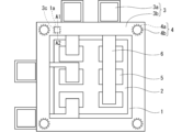
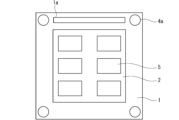
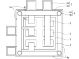
- FIG. 11 is a plan view showing a configuration of a semiconductor device according to a first embodiment
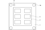
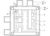
- 1 is a plan view of a semiconductor device according to a first embodiment, in which a resin case is omitted
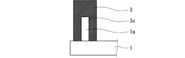
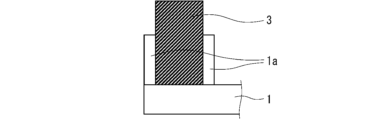
- 2 is a cross-sectional view taken along the line A1-A2 shown in FIG. 1.
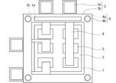
- FIG. 11 is a plan view showing a configuration of a semiconductor device according to a second embodiment.
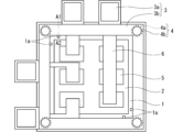
- FIG. 11 is a plan view of a semiconductor device according to a second embodiment, in which a resin case is omitted.
- FIG. 11 is a plan view showing a configuration of a semiconductor device according to a third embodiment.
- FIG. 7 is an enlarged view of a region R shown in FIG. 6 .
- FIG. 7 is an enlarged view of a region R shown in FIG. 6 .
- FIG. 13 is a plan view showing a configuration of a semiconductor device according to a fourth embodiment.
- FIG. 13 is a plan view of a semiconductor device according to a fourth embodiment, in which the resin case is omitted.
- FIG. 13 is a plan view showing a configuration of a semiconductor device according to a fifth embodiment.
- FIG. 13 is a plan view of a semiconductor device according to a fifth embodiment, in which the resin case is omitted.
- 11 is a cross-sectional view taken along the line A1-A2 shown in FIG. 10.
- FIG. 13 is a plan view showing a configuration of a semiconductor device according to a sixth embodiment.
- FIG. 13 is a plan view of a semiconductor device according to a sixth embodiment, in which the resin case is omitted.
- FIG. 14 is a cross-sectional view taken along the line A1-A2 shown in FIG. 13.
- FIG. 23 is a plan view showing a configuration of a semiconductor device according to a seventh embodiment.
- FIG. 13 is a plan view of a semiconductor device according to a seventh embodiment, in which the resin case is omitted.
- 17 is a cross-sectional view taken along the line A1-A2 shown in FIG. 16.
- Figures 1, 2 and 3 are diagrams showing the configuration of a semiconductor device according to embodiment 1.
- Figure 1 is a plan view of the semiconductor device
- Figure 2 is a plan view of the semiconductor device with a resin case omitted from Figure 1
- Figure 3 is a cross-sectional view taken along line A1-A2 shown in Figure 1.
- the semiconductor device includes a semiconductor element 5, an insulating substrate 2 on which the semiconductor element 5 is mounted, a metal base plate 1 on which the insulating substrate 2 is mounted, and a resin case 3 provided on the metal base plate 1 so as to surround the insulating substrate 2.
- the metal base plate 1 is made of a material with excellent thermal conductivity, such as aluminum alloy or copper.
- the insulating substrate 2 is made of an insulating layer and a circuit pattern bonded to both sides of the insulating layer.
- the insulating layer is made of ceramics with excellent thermal conductivity, such as aluminum nitride or silicon nitride, or resin
- the circuit pattern is made of a conductive material with excellent thermal conductivity, such as aluminum alloy or copper.
- the insulating layer and the circuit pattern are bonded by a bonding material, such as solder or soft solder.
- the semiconductor element 5 is bonded to the circuit pattern on the insulating substrate 2 using a bonding material.
- multiple semiconductor elements 5 are mounted on metal lead electrodes 6, and the multiple semiconductor elements 5 are connected via the metal lead electrodes 6 to form a circuit.
- aluminum wires may be used.
- semiconductor element 5 there are no restrictions on the type of semiconductor element 5.
- silicon (Si) IGBTs, diodes, and reverse conducting IGBTs are often used as the semiconductor elements 5.
- MOSFETs and Schottky diodes made of semiconductor materials with a larger band gap than Si, such as silicon carbide (SiC) and gallium nitride (GaN)-based semiconductors, can also be used as the semiconductor elements 5 in power control semiconductor devices.
- SiC silicon carbide
- GaN gallium nitride
- the resin case 3 consists of an external electrode 3a and a resin part 3b.
- the external electrode 3a may be insert molded into the resin part 3b, or may be inserted and placed after the resin part 3b is formed.
- the material of the resin part 3b is generally a highly heat-resistant resin such as PPS (polyphenylene sulfide) or PBT (polybutylene terephthalate), but is not limited to this, and any resin with the desired characteristics may be selected.
- the resin case 3 is filled with a highly insulating sealing resin or the like, which seals the semiconductor element 5, insulating substrate 2, metal lead electrodes 6, etc.
- Typical sealing resins are silicone gel and epoxy resin, but are not limited to these, and any resin having the desired physical properties such as elastic modulus, heat resistance, adhesiveness, and linear expansion coefficient can be selected.
- the semiconductor device has fastening holes 4 at the four corners.
- the fastening holes 4 penetrate the metal base plate 1 and the resin case 3.
- the fastening holes 4 consist of fastening hole 4a, which is a first fastening hole formed in the metal base plate 1, and fastening hole 4b, which is a second fastening hole formed in the resin case 3.
- Fastening hole 4a in the metal base plate 1 and fastening hole 4b in the resin case 3 are arranged so as to overlap.
- a protrusion 1a is provided on the upper surface of the metal base plate 1 to limit the rotation of the resin case 3.
- the protrusion 1a is provided in the area between adjacent fastening holes 4a of the metal base plate 1.
- the protrusion 1a is provided in one or more places on the metal base plate 1, and as long as it can limit the rotation of the resin case 3, its position, shape, and length (height) are not important.
- the position of the protrusion 1a may be anywhere in the area between adjacent fastening holes 4a of the metal base plate 1.
- the shape of the protrusion 1a is shown as a square prism in this example, but it may also be, for example, a cylinder, a tapered pyramid, or a cone.
- a groove 3c is provided on the bottom surface of the resin case 3 (i.e., the surface that abuts against the metal base plate 1) at a position corresponding to the protrusion 1a of the metal base plate 1.
- the resin case 3 is positioned so that the protrusion 1a fits into the groove 3c, as shown in Figure 3, and is mounted on the metal base plate 1.
- the assembly process includes the following first to fifth steps.
- the metal base plate 1, the insulating substrate 2, and the semiconductor element 5 are bonded together using a bonding material such as a solder plate, a solder paste, or other soft solder.
- a bonding material such as a solder plate, a solder paste, or other soft solder.
- solder is often used as the bonding material.
- the bonding step is carried out at a temperature exceeding the melting point of the bonding material used.
- the bonding material may be a preformed material such as a solder plate, or may be a solder paste that is applied by screen printing, dispensing, or the like.
- a silicone or epoxy adhesive is applied to the outer periphery of the metal base plate 1 to be joined to the resin case 3, and the metal base plate 1 is placed on a jig. Then, the resin case 3 is placed on the metal base plate 1, and these are fastened together with the jig with screws to pressure-weld the metal base plate 1 and the resin case 3. In this state, the metal base plate 1 and the resin case 3 are heated to cure the adhesive.
- the control electrode (not shown) of the semiconductor element 5 and an external signal terminal (not shown) for inputting a control signal are connected by ultrasonic bonding of a wire, etc.
- Aluminum which has high thermal conductivity and electrical conductivity, is often used as the material for this wire.
- the resin case 3 is filled with a sealing resin to seal the semiconductor element 5, the insulating substrate 2, the metal lead electrodes 6, etc.
- the sealing resin is often silicone gel or epoxy resin, but is not limited thereto, and any resin having the desired elastic modulus and physical properties such as heat resistance, adhesiveness, linear expansion coefficient, etc. may be selected.
- the semi-finished product is then placed in a curing furnace or the like to harden the sealing resin.
- the metal base plate 1 has a protrusion 1a
- the resin case 3 has a groove 3c into which the protrusion 1a fits. Therefore, when the metal base plate 1 and the resin case 3 are screwed together in the second step, the torque of the screws is limited to prevent the resin case 3 from rotating. This prevents misalignment between the fastening hole 4a in the metal base plate 1 and the fastening hole 4b in the resin case 3.
- FIG. 4 is a plan view of the semiconductor device
- Fig. 5 is a plan view of the semiconductor device from Fig. 4 with the resin case thereof omitted.
- the shape of the protrusion 1a provided on the metal base plate 1 is linear (i.e., a long rectangular shape) in a plan view. That is, the metal base plate 1 has linear protrusions 1a extending between adjacent fastening holes 4a. Furthermore, the resin case 3 is provided with linear grooves 3c in which the linear protrusions 1a fit at positions corresponding to the protrusions 1a of the metal base plate 1. The protrusions 1a are provided in one or more places on the metal base plate 1.
- the protrusion 1a of the metal base plate 1 limits the rotation of the resin case 3 caused by the torque of the screw tightening in the second step.
- the amount of deviation in the rotational direction of the metal base plate 1 is suppressed more than in the first embodiment, and misalignment between the fastening hole 4a of the metal base plate 1 and the fastening hole 4b of the resin case 3 is even less likely to occur.
- ⁇ Third embodiment> 6 and 7 are diagrams showing the configuration of a semiconductor device according to a third embodiment of the present invention.
- Fig. 6 is a plan view of the semiconductor device
- Fig. 7 is an enlarged view of a region R shown in Fig. 6.
- FIG. 6 shows a state in which the position of the resin case 3 is shifted relative to the metal base plate 1, but the groove 3c of the resin case 3 is caught on the protrusion 1a of the metal base plate 1, preventing the shift of the resin case 3.
- Figure 7 shows the positional relationship between the protrusion 1a of the metal base plate 1 and the groove 3c of the resin case 3 in the state shown in Figure 6, as well as the positional relationship between the fastening hole 4a of the metal base plate 1 and the fastening hole 4b of the resin case 3.
- the maximum width Wmax of the gap that can be formed between the protrusion 1a fitted into the groove 3c and the inner wall of that groove 3c is smaller than the difference between the diameter Da of the fastening hole 4a of the metal base plate 1 and the diameter Db of the fastening hole 4b of the resin case 3.
- holds.
- holds, so even if the resin case 3 rotates due to the torque of the screws tightened in the second process, the inner wall of the groove 3c of the resin case 3 catches on the protrusion 1a of the metal base plate 1 before the fastening hole 4b of the resin case 3 protrudes from the fastening hole 4a of the metal base plate 1. Therefore, there is substantially no misalignment between the fastening hole 4a of the metal base plate 1 and the fastening hole 4b of the resin case 3.
- ⁇ Fourth embodiment> 8 and 9 are diagrams showing the configuration of a semiconductor device according to the fourth embodiment.
- Fig. 8 is a plan view of the semiconductor device
- Fig. 9 is a plan view of the semiconductor device from Fig. 8 with the resin case of the semiconductor device omitted.
- a plurality of cylindrical protrusions 1a are provided on the metal base plate 1.
- the resin case 3 also has a plurality of circular grooves 3c into which the plurality of cylindrical protrusions 1a fit.
- the position of the cylindrical protrusions 1a may be anywhere in the region between adjacent fastening holes 4a on the metal base plate 1.
- Fig. 10, Fig. 11 and Fig. 12 are diagrams showing the configuration of a semiconductor device according to embodiment 5.
- Fig. 10 is a plan view of the semiconductor device
- Fig. 11 is a plan view of the semiconductor device with a resin case omitted from Fig. 10
- Fig. 12 is a cross-sectional view taken along line A1-A2 shown in Fig. 10.
- one or more pairs of protrusions 1a are provided on each of two non-parallel sides of the metal base plate 1, and the protrusions 1a are arranged to sandwich a part of the resin case 3.
- the protrusions 1a are arranged to sandwich a part of the resin case 3.
- the protrusions 1a of the metal base plate 1 limit the rotation of the resin case 3 due to the torque of the screws tightened in the second step.
- the pair of protrusions 1a are configured to clamp a part of the metal base plate 1, there is no need to form a groove 3c in the resin case 3.
- Fig. 13, Fig. 14, and Fig. 15 are diagrams showing the configuration of a semiconductor device according to embodiment 6.
- Fig. 13 is a plan view of the semiconductor device
- Fig. 14 is a plan view of the semiconductor device with the resin case of the semiconductor device omitted from Fig. 13
- Fig. 15 is a cross-sectional view taken along line A1-A2 shown in Fig. 13.
- one or more protrusions 1a are provided on each side of the metal base plate 1 and are arranged on the inside of the resin case 3.
- the metal base plate 1 has four or more protrusions 1a on the inside of the resin case 3.
- the resin case 3 is arranged on the metal base plate 1, the multiple protrusions 1a are fitted into the inside of the resin case 3.
- the protrusions 1a of the metal base plate 1 limit the rotation of the resin case 3 due to the torque of the screws tightened in the second step.
- horizontal deviation of the metal base plate 1 is also suppressed, making it even less likely that misalignment will occur between the fastening holes 4a of the metal base plate 1 and the fastening holes 4b of the resin case 3.
- the inner wall of the resin case 3 is configured to engage with the protrusions 1a, there is no need to form grooves 3c in the resin case 3. This is effective in cases where it is difficult to position some of the protrusions 1a on the outside of the resin case 3, as in the fifth embodiment.
- Fig. 16, Fig. 17, and Fig. 18 are diagrams showing the configuration of a semiconductor device according to embodiment 7.
- Fig. 16 is a plan view of the semiconductor device
- Fig. 17 is a plan view of the semiconductor device with the resin case of the semiconductor device omitted from Fig. 16
- Fig. 18 is a cross-sectional view taken along line A1-A2 shown in Fig. 16.
- one or more protrusions 1a are provided on each side of the metal base plate 1 and are arranged on the outside of the resin case 3. Therefore, the metal base plate 1 is provided with four or more protrusions 1a on the outside of the resin case 3. When the resin case 3 is placed on the metal base plate 1, the protrusions 1a on each side are positioned on the outside of the resin case 3.
- the protrusions 1a of the metal base plate 1 limit the rotation of the resin case 3 due to the torque of the screws tightened in the second step. Also, as in embodiment 6, the provision of protrusions 1a on each side of the metal base plate 1 also suppresses horizontal deviation of the metal base plate 1, making it even less likely that misalignment will occur between the fastening holes 4a of the metal base plate 1 and the fastening holes 4b of the resin case 3. Also, since the outer wall of the resin case 3 is configured to engage with the protrusions 1a, there is no need to form grooves 3c in the resin case 3. This is effective when it is difficult to arrange all of the protrusions 1a inside the resin case 3 as in embodiment 6.
- the basic configuration of the semiconductor device according to the eighth embodiment is the same as that of the fifth, sixth or seventh embodiment, and further, the maximum width of the gap that can be formed between the resin case 3 mounted on the metal base plate 1 and the protrusion 1a of the metal base plate 1 is designed to be smaller than the difference between the diameter of the fastening hole 4b and the diameter of the fastening hole 4a of the resin case 3.
- Wmax the maximum width of the gap between the resin case 3 and the protrusion 1a of the metal base plate 1
- the diameter of the fastening hole 4b of the resin case 3 is Da
- the diameter of the fastening hole 4a is Db
- is established.
- holds, so even if the resin case 3 rotates due to the torque of the screws tightened in the second process, the resin case 3 will catch on the protrusion 1a of the metal base plate 1 before the fastening hole 4b of the resin case 3 protrudes from the fastening hole 4a of the metal base plate 1. Therefore, there is substantially no misalignment between the fastening hole 4a of the metal base plate 1 and the fastening hole 4b of the resin case 3.
Landscapes
- Structures Or Materials For Encapsulating Or Coating Semiconductor Devices Or Solid State Devices (AREA)
Abstract
Description
図1、図2および図3は、実施の形態1に係る半導体装置の構成を示す図である。図1は、当該半導体装置の平面図であり、図2は、図1から半導体装置の樹脂ケースを省略した平面図であり、図3は、図1に示すA1-A2線に沿った断面図である。
第1工程では、金属ベース板1、絶縁基板2および半導体素子5を、板はんだやはんだペースト、その他の軟ろうなどの接合材を用いて接合する。一般的には、接合材としてはんだが用いられることが多い。接合工程は、用いられる接合材の融点を超える温度で行われる。接合材は、板はんだなど、あらかじめ成形されたものでもよいし、はんだペーストなど、スクリーン印刷やディスペンス等で塗布されるものでもよい。
第2工程では、樹脂ケース3と接合する金属ベース板1の外周部にシリコーン系やエポキシ系の接着剤を塗布し、金属ベース板1を治具の上に載置する。その後、金属ベース板1の上に樹脂ケース3を載せ、それらを治具とともにねじで締結することで、金属ベース板1と樹脂ケース3とを圧接させる。その状態で、金属ベース板1および樹脂ケース3を加熱して、接着剤をキュアする。
第3工程では、半導体素子5に金属リード電極6をはんだ接合することにより、回路を形成する。第2工程で取り付けたねじは、第3工程よりも後に取り外される。
第4工程では、半導体素子5の制御電極(不図示)と制御信号入力用の外部信号端子(不図示)とを、ワイヤの超音波接合などにより接続させる。このワイヤの材料としては、熱伝導性や電気伝導率の高いアルミニウム等が用いられることが多い。
第5工程では、樹脂ケース3内に封止樹脂を充填することで、半導体素子5、絶縁基板2、金属リード電極6などを封止する。封止樹脂は、シリコーンゲルやエポキシ樹脂を用いることが多いが、これに限定されず、所望の弾性率と耐熱性や接着性、線膨張係数などの物性を有しているものが選択されればよい。その後、半製品をキュア炉などに入れ、封止樹脂を硬化させる。
図4および図5は、実施の形態2に係る半導体装置の構成を示す図である。図4は、当該半導体装置の平面図であり、図5は、図4から半導体装置の樹脂ケースを省略した平面図である。
図6および図7は、実施の形態3に係る半導体装置の構成を示す図である。図6は、当該半導体装置の平面図であり、図7は、図6に示す領域Rの拡大図である。
図8および図9は、実施の形態4に係る半導体装置の構成を示す図である。図8は、当該半導体装置の平面図であり、図9は、図8から半導体装置の樹脂ケースを省略した平面図である。
図10、図11および図12は、実施の形態5に係る半導体装置の構成を示す図である。図10は、当該半導体装置の平面図であり、図11は、図10から半導体装置の樹脂ケースを省略した平面図であり、図12は、図10に示すA1-A2線に沿った断面図である。
図13、図14および図15は、実施の形態6に係る半導体装置の構成を示す図である。図13は、当該半導体装置の平面図であり、図14は、図13から半導体装置の樹脂ケースを省略した平面図であり、図15は、図13に示すA1-A2線に沿った断面図である。
図16、図17および図18は、実施の形態7に係る半導体装置の構成を示す図である。図16は、当該半導体装置の平面図であり、図17は、図16から半導体装置の樹脂ケースを省略した平面図であり、図18は、図16に示すA1-A2線に沿った断面図である。
実施の形態8に係る半導体装置の基本的な構成は、実施の形態5、6または7と同様であり、さらに、金属ベース板1に搭載された樹脂ケース3と金属ベース板1の突起1aとの間に形成され得る隙間の最大幅が、樹脂ケース3の締結穴4bの径と締結穴4aの径との差よりも小さくなるように設計されている。すなわち、樹脂ケース3と金属ベース板1の突起1aとの間の隙間の最大幅をWmax、樹脂ケース3の締結穴4bの径をDa、締結穴4aの径をDbとすると、Wmax<|Da-Db|の関係が成り立つ。
Claims (9)
- 半導体素子と、
前記半導体素子を搭載する絶縁基板と、
前記絶縁基板を搭載する金属ベース板と、
前記金属ベース板の上に前記絶縁基板を囲うように設けられた樹脂ケースと、
前記金属ベース板に形成された複数の第1の締結穴と、
前記樹脂ケースに形成され、複数の前記第1の締結穴と重なるように配置された複数の第2の締結穴と、
前記金属ベース板の隣り合う前記第1の締結穴の間の領域に設けられ、前記樹脂ケースの回動を制限する突起と、
を備える半導体装置。 - 前記樹脂ケースは、前記突起が嵌合する溝を備える、
請求項1に記載の半導体装置。 - 前記金属ベース板は、隣り合う前記第1の締結穴の間に延在するライン状の前記突起を備え、
前記樹脂ケースは、ライン状の前記突起が嵌合するライン状の前記溝を備える、
請求項2に記載の半導体装置。 - 前記金属ベース板は、円柱状の前記突起を複数備え、
前記樹脂ケースは、複数の円柱状の前記突起が嵌合する複数の円形の前記溝を備える、
請求項2に記載の半導体装置。 - 前記溝に嵌合した前記突起と前記溝の内壁との間に形成され得る隙間の最大幅は、前記第1の締結穴の径と前記第2の締結穴の径との差よりも小さい、
請求項2から請求項4のいずれか一項に記載の半導体装置。 - 前記金属ベース板は、前記金属ベース板の互いに並行でない2つの辺のそれぞれに、前記樹脂ケースの一部を挟むように配置された1対の前記突起を備える、
請求項1に記載の半導体装置。 - 前記金属ベース板は、前記金属ベース板のそれぞれの辺に、前記樹脂ケースの内側に配置された前記突起を備える、
請求項1に記載の半導体装置。 - 前記金属ベース板は、前記金属ベース板のそれぞれの辺に、前記樹脂ケースの外側に配置された前記突起を備える、
請求項1に記載の半導体装置。 - 前記金属ベース板に搭載された前記樹脂ケースと前記突起との間に形成され得る隙間の最大幅は、前記第2の締結穴の径と前記第1の締結穴の径との差よりも小さい、
請求項6から請求項8のいずれか一項に記載の半導体装置。
Priority Applications (4)
| Application Number | Priority Date | Filing Date | Title |
|---|---|---|---|
| JP2024569967A JP7822489B2 (ja) | 2023-01-13 | 2023-01-13 | 半導体装置 |
| DE112023005560.2T DE112023005560T5 (de) | 2023-01-13 | 2023-01-13 | Halbleitervorrichtung |
| CN202380085591.4A CN120435765A (zh) | 2023-01-13 | 2023-01-13 | 半导体装置 |
| PCT/JP2023/000733 WO2024150397A1 (ja) | 2023-01-13 | 2023-01-13 | 半導体装置 |
Applications Claiming Priority (1)
| Application Number | Priority Date | Filing Date | Title |
|---|---|---|---|
| PCT/JP2023/000733 WO2024150397A1 (ja) | 2023-01-13 | 2023-01-13 | 半導体装置 |
Publications (1)
| Publication Number | Publication Date |
|---|---|
| WO2024150397A1 true WO2024150397A1 (ja) | 2024-07-18 |
Family
ID=91896638
Family Applications (1)
| Application Number | Title | Priority Date | Filing Date |
|---|---|---|---|
| PCT/JP2023/000733 Ceased WO2024150397A1 (ja) | 2023-01-13 | 2023-01-13 | 半導体装置 |
Country Status (4)
| Country | Link |
|---|---|
| JP (1) | JP7822489B2 (ja) |
| CN (1) | CN120435765A (ja) |
| DE (1) | DE112023005560T5 (ja) |
| WO (1) | WO2024150397A1 (ja) |
Citations (2)
| Publication number | Priority date | Publication date | Assignee | Title |
|---|---|---|---|---|
| JPH09107059A (ja) * | 1995-10-11 | 1997-04-22 | Toshiba Corp | 半導体装置及びその製造方法 |
| JP2004103846A (ja) * | 2002-09-10 | 2004-04-02 | Mitsubishi Electric Corp | 電力用半導体装置 |
-
2023
- 2023-01-13 DE DE112023005560.2T patent/DE112023005560T5/de active Pending
- 2023-01-13 WO PCT/JP2023/000733 patent/WO2024150397A1/ja not_active Ceased
- 2023-01-13 CN CN202380085591.4A patent/CN120435765A/zh active Pending
- 2023-01-13 JP JP2024569967A patent/JP7822489B2/ja active Active
Patent Citations (2)
| Publication number | Priority date | Publication date | Assignee | Title |
|---|---|---|---|---|
| JPH09107059A (ja) * | 1995-10-11 | 1997-04-22 | Toshiba Corp | 半導体装置及びその製造方法 |
| JP2004103846A (ja) * | 2002-09-10 | 2004-04-02 | Mitsubishi Electric Corp | 電力用半導体装置 |
Also Published As
| Publication number | Publication date |
|---|---|
| CN120435765A (zh) | 2025-08-05 |
| DE112023005560T5 (de) | 2025-10-30 |
| JPWO2024150397A1 (ja) | 2024-07-18 |
| JP7822489B2 (ja) | 2026-03-02 |
Similar Documents
| Publication | Publication Date | Title |
|---|---|---|
| US6601294B1 (en) | Method for making a packaged semiconductor device | |
| CN104285294B (zh) | 半导体装置及该半导体装置的制造方法 | |
| CN104517913A (zh) | 半导体装置及其制造方法 | |
| US20130270688A1 (en) | Power module | |
| US9583407B2 (en) | Semiconductor device | |
| JP2008288414A (ja) | 半導体モジュール及び半導体モジュールの製造方法 | |
| JP6057927B2 (ja) | 半導体装置 | |
| CN105612613A (zh) | 半导体装置 | |
| JP4385324B2 (ja) | 半導体モジュールおよびその製造方法 | |
| WO2023214500A1 (ja) | 半導体装置 | |
| JP2010050395A (ja) | 半導体装置およびその製造方法 | |
| CN114078790A (zh) | 功率半导体模块装置及其制造方法 | |
| JP7152502B2 (ja) | 半導体装置及びその製造方法 | |
| JP7822489B2 (ja) | 半導体装置 | |
| CN108292642B (zh) | 电力用半导体装置 | |
| WO2024181147A1 (ja) | 半導体装置および車両 | |
| JP6906654B2 (ja) | 半導体装置およびその製造方法 | |
| JPH09237869A (ja) | 樹脂封止型パワーモジュール装置及びその製造方法 | |
| JP7482833B2 (ja) | 半導体装置および半導体装置の製造方法 | |
| WO2017077729A1 (ja) | 半導体モジュール及びその製造方法 | |
| JP7489933B2 (ja) | 半導体装置及びその製造方法 | |
| JP7496796B2 (ja) | 半導体装置 | |
| JP7672574B2 (ja) | 半導体装置 | |
| US20250285937A1 (en) | Housing, semiconductor module comprising a housing, and method for assembling a semiconductor module | |
| JP6887476B2 (ja) | 半導体パワーモジュール |
Legal Events
| Date | Code | Title | Description |
|---|---|---|---|
| 121 | Ep: the epo has been informed by wipo that ep was designated in this application |
Ref document number: 23916018 Country of ref document: EP Kind code of ref document: A1 |
|
| WWE | Wipo information: entry into national phase |
Ref document number: 2024569967 Country of ref document: JP |
|
| WWE | Wipo information: entry into national phase |
Ref document number: 202380085591.4 Country of ref document: CN |
|
| WWP | Wipo information: published in national office |
Ref document number: 202380085591.4 Country of ref document: CN |
|
| WWE | Wipo information: entry into national phase |
Ref document number: 112023005560 Country of ref document: DE |
|
| WWP | Wipo information: published in national office |
Ref document number: 112023005560 Country of ref document: DE |
|
| 122 | Ep: pct application non-entry in european phase |
Ref document number: 23916018 Country of ref document: EP Kind code of ref document: A1 |