WO2024142679A1 - 積層セラミックコンデンサ - Google Patents
積層セラミックコンデンサ Download PDFInfo
- Publication number
- WO2024142679A1 WO2024142679A1 PCT/JP2023/041870 JP2023041870W WO2024142679A1 WO 2024142679 A1 WO2024142679 A1 WO 2024142679A1 JP 2023041870 W JP2023041870 W JP 2023041870W WO 2024142679 A1 WO2024142679 A1 WO 2024142679A1
- Authority
- WO
- WIPO (PCT)
- Prior art keywords
- internal electrode
- electrode layer
- layer
- distance
- face
- Prior art date
- Legal status (The legal status is an assumption and is not a legal conclusion. Google has not performed a legal analysis and makes no representation as to the accuracy of the status listed.)
- Ceased
Links
Images








Classifications
-
- H—ELECTRICITY
- H01—ELECTRIC ELEMENTS
- H01G—CAPACITORS; CAPACITORS, RECTIFIERS, DETECTORS, SWITCHING DEVICES, LIGHT-SENSITIVE OR TEMPERATURE-SENSITIVE DEVICES OF THE ELECTROLYTIC TYPE
- H01G4/00—Fixed capacitors; Processes of their manufacture
- H01G4/002—Details
- H01G4/005—Electrodes
- H01G4/012—Form of non-self-supporting electrodes
-
- H—ELECTRICITY
- H01—ELECTRIC ELEMENTS
- H01G—CAPACITORS; CAPACITORS, RECTIFIERS, DETECTORS, SWITCHING DEVICES, LIGHT-SENSITIVE OR TEMPERATURE-SENSITIVE DEVICES OF THE ELECTROLYTIC TYPE
- H01G4/00—Fixed capacitors; Processes of their manufacture
- H01G4/002—Details
- H01G4/018—Dielectrics
- H01G4/06—Solid dielectrics
- H01G4/08—Inorganic dielectrics
- H01G4/12—Ceramic dielectrics
-
- H—ELECTRICITY
- H01—ELECTRIC ELEMENTS
- H01G—CAPACITORS; CAPACITORS, RECTIFIERS, DETECTORS, SWITCHING DEVICES, LIGHT-SENSITIVE OR TEMPERATURE-SENSITIVE DEVICES OF THE ELECTROLYTIC TYPE
- H01G4/00—Fixed capacitors; Processes of their manufacture
- H01G4/002—Details
- H01G4/228—Terminals
- H01G4/232—Terminals electrically connecting two or more layers of a stacked or rolled capacitor
-
- H—ELECTRICITY
- H01—ELECTRIC ELEMENTS
- H01G—CAPACITORS; CAPACITORS, RECTIFIERS, DETECTORS, SWITCHING DEVICES, LIGHT-SENSITIVE OR TEMPERATURE-SENSITIVE DEVICES OF THE ELECTROLYTIC TYPE
- H01G4/00—Fixed capacitors; Processes of their manufacture
- H01G4/002—Details
- H01G4/228—Terminals
- H01G4/248—Terminals the terminals embracing or surrounding the capacitive element, e.g. caps
-
- H—ELECTRICITY
- H01—ELECTRIC ELEMENTS
- H01G—CAPACITORS; CAPACITORS, RECTIFIERS, DETECTORS, SWITCHING DEVICES, LIGHT-SENSITIVE OR TEMPERATURE-SENSITIVE DEVICES OF THE ELECTROLYTIC TYPE
- H01G4/00—Fixed capacitors; Processes of their manufacture
- H01G4/30—Stacked capacitors
Definitions
- Patent Document 2 also discloses a configuration in which an auxiliary layer is provided in a recess formed by a step caused by the thickness of the internal electrode layer. This auxiliary layer is formed so that it rides up onto the edge of the internal electrode layer in order to reduce the occurrence of defects caused by the recess.
- the present invention provides a laminate having a plurality of laminated dielectric layers and a plurality of internal electrode layers laminated on the dielectric layers, the laminate having a first main surface and a second main surface opposed to each other in a lamination direction, a first end face and a second end face opposed to each other in a length direction perpendicular to the lamination direction, and a first side face and a second side face opposed to each other in a width direction perpendicular to the lamination direction and the length direction;
- a multilayer ceramic capacitor having a plurality of external electrodes
- the plurality of internal electrode layers include a plurality of first internal electrode layers and a plurality of second internal electrode layers, the first internal electrode layer has a first opposing portion opposing the second internal electrode layer via the dielectric layer, and a first lead portion extending from the first opposing portion and led to the first end face of the laminate, the first extension portion has a first transition region in which the length in the width direction gradually decreases, and a first extension region that extends from the
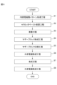
- FIG. 5A to 5C are process diagrams illustrating a manufacturing method of the multilayer ceramic capacitor 200 (second embodiment).
- 5A to 5C are process diagrams illustrating a manufacturing method of the multilayer ceramic capacitor 200 (second embodiment).
- 5A to 5C are process diagrams illustrating a manufacturing method of the multilayer ceramic capacitor 200 (second embodiment).
- 5A to 5C are process diagrams illustrating a manufacturing method of the multilayer ceramic capacitor 200 (second embodiment).
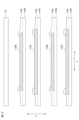
- FIG. 1 is a schematic perspective view of the multilayer ceramic capacitor 1.
- FIG. 2 shows a cross section (WT cross section) of the multilayer ceramic capacitor 1 cut along line II-II in FIG. 1 and defined by the width direction W and the stacking direction T, and shows the upper half of ...
- the embodiments are illustrative of the embodiments of the present invention, and the present invention is not limited to the contents of the embodiments. It is also possible to combine the contents described in different embodiments, and the contents of such combinations are also included in the present invention.
- the drawings are intended to aid in understanding the specification, and may be drawn diagrammatically, and the dimensional ratios of the depicted components or between the components may not match those dimensional ratios described in the specification. Components described in the specification may be omitted in the drawings, or may be drawn with the number of components omitted.
- the multilayer ceramic capacitor 1 comprises end surface external electrodes 3 provided on both end surfaces C in the length direction L of the laminate 2, and side surface external electrodes 4 provided on both side surfaces B in the width direction W of the laminate 2.
- the laminate 2 comprises an inner layer portion 11 including multiple pairs of dielectric layers 14 and internal electrode layers 15, and an outer layer portion 12.
- the dimensions of the multilayer ceramic capacitor 1 are not particularly limited, but the length direction L can be 0.6 mm or more and 3.2 mm or less, the stacking direction T can be 0.3 mm or more and 2.5 mm or less, and the width direction W can be 0.3 mm or more and 2.5 mm or less.
- the term used to indicate the orientation of the multilayer ceramic capacitor 1 refers to the direction in which the dielectric layers 14 and the internal electrode layers 15 are stacked in the multilayer ceramic capacitor 1 as the stacking direction T.
- the direction that intersects with the stacking direction T and in which the pair of end face external electrodes 3 are provided is referred to as the length direction L.
- the direction that intersects with both the length direction L and the stacking direction T is referred to as the width direction W. Note that in the embodiment, the stacking direction T, the length direction L, and the width direction W are mutually orthogonal.
- the laminate 2 includes an inner layer portion 11 and outer layer portions 12 disposed on both sides of the inner layer portion 11 in the stacking direction T. It is preferable that the corners and ridges of the laminate 2 are rounded. The corners are portions where three surfaces of the laminate intersect, and the ridges are portions where two surfaces of the laminate intersect.
- the dimensions of the laminate 2 are not particularly limited, but the length direction L can be 0.6 mm or more and 3.2 mm or less, the stacking direction T can be 0.3 mm or more and 2.5 mm or less, and the width direction W can be 0.3 mm or more and 2.5 mm or less.
- the inner layer portion 11 includes a plurality of dielectric layers 14 and a plurality of internal electrode layers 15 laminated in a lamination direction T.
- the dielectric layer 14 is made of a ceramic material.
- a dielectric ceramic containing BaTiO3 as a main component is used as the ceramic material.
- the ceramic material may be one containing at least one of a Mn compound, an Fe compound, a Cr compound, a Co compound, a Ni compound, or the like, in addition to the main component.
- the dielectric layer 14 includes a dielectric layer 14c manufactured from a ceramic green sheet 114 described below, and dielectric layers 14a and 14b manufactured from ceramic pastes 114a, 114b applied onto the ceramic green sheet 114.
- the internal electrode layers 15 are preferably made of a metal material such as Ni, Cu, Ag, Pd, an Ag-Pd alloy, or Au.
- the internal electrode layer 15 has a first internal electrode layer 15A and a second internal electrode layer 15B that are arranged alternately, and the first internal electrode layer 15A and the second internal electrode layer 15B form a capacitance via the dielectric layer 14 at the first opposing portion 15Aa and the second opposing portion 15Ba that overlap each other when viewed in a plan view from the stacking direction T.
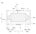
- FIG. 4 is a cross-sectional view taken along the first internal electrode layer 15A of the multilayer ceramic capacitor 1. As shown in Fig. 4, the first internal electrode layer 15A extends between both end faces C in the longitudinal direction L of the laminate 2 as a whole, and is spaced a fixed distance from both side faces B in the width direction W.
- the first internal electrode layer 15A is composed of a rectangular first opposing portion 15Aa that is a certain distance away from both end faces C and faces a second opposing portion 15Ba of the second internal electrode layer 15B described below across the dielectric layer 14, and a first lead portion 15Ab1 and a second lead portion 15Ab2 that extend from the first opposing portion 15Aa to a first end face C1 and a second end face C2, respectively.
- the first lead portion 15Ab1 is composed of a trapezoidal first transition region 15At1 whose length in the width direction W gradually decreases toward the first end face C1, and a first extension region 15Aw1 that further extends from the first transition region 15At1 to the first end face C1.
- the second draw-out portion 15Ab2 is composed of a trapezoidal second transition region 15At2 whose length in the width direction W gradually decreases toward the second end face C2, and a second extension region 15Aw2 that extends from the second transition region 15At2 to the second end face C2.
- the first extension region 15Aw1 and the second extension region 15Aw2 are exposed at the first end face C1 and the second end face C2, respectively, and are connected to the first end face external electrode 3a and the second end face external electrode 3b, respectively.
- the length in the width direction W of the first extension region 15Aw1 of the first extension portion 15Ab1 and the second extension region 15Aw2 of the second extension portion 15Ab2 is shorter than the length in the width direction W of the first opposing portion 15Aa. In this way, by shortening the length in the width direction W of the first extension region 15Aw1 and the second extension region 15Aw2, it is possible to suppress the intrusion of moisture from the outside, thereby improving the reliability of the multilayer ceramic capacitor.
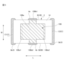
- Fig. 5 is a cross-sectional view taken along the second internal electrode layer 15B of the multilayer ceramic capacitor 1.
- the second internal electrode layer 15B is slightly smaller than the laminate 2, and has a rectangular second opposing portion 15Ba whose sides are spaced a fixed distance from the end face C and the side face B, and a first lead portion 15Bb1 and a second lead portion 15Bb2 extending from the second opposing portion 15Ba to the first side face B1 and the second side face B2, respectively.
- the second opposing portion 15Ba has a first marginal region 15Be1 along one side on the first end face C1 side, and a second marginal region 15Be2 along one side on the second end face C2 side.
- the first lead portion 15Bb1 and the second lead portion 15Bb2 are exposed to the first side surface B1 and the second side surface B2 of the laminate 2, respectively, and are connected to the first side surface external electrode 4a and the second side surface external electrode 4b.
- the length in the longitudinal direction L of the first lead portion 15Bb1 and the second lead portion 15Bb2 is shorter than the length in the longitudinal direction L of the second opposing portion 15Ba. In this way, by shortening the length in the longitudinal direction L of the first lead portion 15Bb1 and the second lead portion 15Bb2, it is possible to suppress the intrusion of moisture from the outside, thereby improving the reliability of the multilayer ceramic capacitor.
- the outer layer portion 12 is a dielectric layer of a constant thickness disposed on the first principal surface A1 side and the second principal surface A2 side of the inner layer portion 11.
- the outer layer portion 12 is made of the same material as the dielectric layer 14 of the inner layer portion 11.
- the thickness of the dielectric layer is not particularly limited, but is preferably 0.3 ⁇ m to 1.5 ⁇ m, and more preferably 0.5 ⁇ m to 1 ⁇ m.
- the laminate 2 consisting of the inner layer 11 and the outer layer 12 can be formed from 14 to 1,000 dielectric layers.
- End surface external electrode 3 A first end surface external electrode 3a is disposed on a first end surface C1 of the laminate 2, and a second end surface external electrode 3b is disposed on a second end surface C2.
- a first lead portion 15Ab1 of the first internal electrode layer 15A is connected to the first end surface external electrode 3a.
- a second lead portion 15Ab2 of the first internal electrode layer 15A is connected to the second end surface external electrode 3b.
- the first end surface external electrode 3a and the second end surface external electrode 3b cover not only the first end surface C1 and the second end surface C2, but also parts of the first main surface A1, the second main surface A2, the first side surface B1, and the second side surface B2, respectively.
- the multilayer ceramic capacitor 1 in which the first internal electrode layer 15A is connected to the first end face external electrode 3a and the second end face external electrode 3b, and the second internal electrode layer 15B is connected to the first side face external electrode 4a and the second side face external electrode 4b, can be used as a three-terminal capacitor. That is, the multilayer ceramic capacitor 1 can be used as a three-terminal capacitor by interrupting the power supply line or signal line in the circuit, connecting the first end face external electrode 3a to one of the interrupted lines, connecting the second end face external electrode 3b to the other of the interrupted lines, and connecting the first side face external electrode 4a and the second side face external electrode 4b to ground. In this case, the first internal electrode layer 15A becomes a through electrode, and the second internal electrode layer 15B becomes a ground electrode.
- the end face external electrode 3 and the side face external electrode 4 can have a structure including, for example, a base electrode layer and a plating layer disposed on the base electrode layer.
- the glass component includes at least one selected from B, Si, Ba, Mg, Al, Li, etc.
- the metal includes at least one selected from Cu, Ni, Ag, Pd, Ag-Pd alloy, Au, etc.
- the thickness of the baked layer is preferably, for example, 3 ⁇ m or more and 70 ⁇ m or less.
- the baked layer may also be multiple layers.
- the conductive resin layer is formed on the surface of the baked layer, or directly on the surface of the laminate.
- the conductive resin layer may be a multi-layered layer.
- the conductive resin layer is formed by applying a conductive resin paste containing a thermosetting resin and a metal component onto a baking layer or a laminate, and then performing a heat treatment at a temperature of 250 to 550°C or higher to thermally cure the resin and form a conductive resin layer.
- the atmosphere during the heat treatment is preferably a N2 atmosphere.
- the thickness of the conductive resin layer at the center of end face C is preferably, for example, 10 ⁇ m or more and 150 ⁇ m or less.
- the metal contained in the conductive resin layer can be Ag, Cu, or an alloy of these.
- Metal powder with an Ag-coated surface can also be used.
- metal powder with an Ag-coated surface it is preferable to use Cu or Ni as the metal powder.
- Cu that has been treated to prevent oxidation can also be used.
- the metal contained in the conductive resin layer is preferably contained in an amount of 35 vol% or more and 75 vol% or less relative to the total volume of the conductive resin.
- the shape of the metal contained in the conductive resin layer is not particularly limited.
- the conductive filler may be spherical, flat, etc.
- the average particle size of the metal contained in the conductive resin layer is not particularly limited, but can be, for example, about 0.3 ⁇ m or more and 10 ⁇ m or less.
- the plating layer preferably contains at least one metal selected from, for example, Cu, Ni, Sn, Pb, Au, Ag, Pd, Bi, or Zn, or an alloy containing the metal.
- the direct plating layer is preferably formed using Cu, which has good bonding properties with Ni.
- each plating layer is preferably 2 ⁇ m or more and 15 ⁇ m or less.
- the plating layer preferably does not contain glass.
- the metal ratio per unit volume of the plating layer is preferably 99 volume % or more.
- the thin film layer is formed by a thin film formation method such as sputtering or vapor deposition, and is a layer of 1 ⁇ m or less in thickness in which metal particles are deposited.
- a first distance T1 which is the distance between adjacent second internal electrode layers 15B in the stacking direction T and which is the distance between the second internal electrode layers that overlap the first internal electrode layer 15A in the stacking direction T in the first edge region 15Be1, has a portion that is longer than a second distance T2, which is the distance between adjacent first internal electrode layers 15A in the stacking direction T and which is the distance between the first internal electrode layers that do not overlap the second internal electrode layer 15B in the stacking direction T in the first transition region 15At1.
- the first distance T1, the second distance T2, the third distance T3, the fourth distance T4, and the fifth distance T5 can be measured at each location by polishing the multilayer ceramic capacitor 1 parallel to the side B along line III-III shown in FIG. 1 to expose the cross section, and observing the cross section with a scanning electron microscope. Specifically, the first distance T1 is measured on a cross section of the multilayer ceramic capacitor 1 that has been polished perpendicular to its width to a position that is half the width of the multilayer ceramic capacitor 1. The cross section is divided into three regions such that the thickness of the inner layer is equally divided into three, and the dimension T1 is measured at 20 points in each region using a scanning electron microscope (SEM). Finally, the average value of these measurements is taken to determine the first distance T1.
- SEM scanning electron microscope
- the second distance T2 is measured by dividing the cross section into three regions so that the thickness dimension of the inner layer is divided into three equal parts, and measuring the T2 dimension at 20 points in each region using a scanning electron microscope (SEM). Finally, the average value of these measurements is taken as the second distance T2.
- the third distance T3 is determined by dividing the cross section into three regions such that the thickness dimension of the inner layer portion is divided into three equal parts, and measuring the dimension T3 at 20 points in each region using a scanning electron microscope (SEM). Finally, the average value of these measurements is taken to determine the third distance T3.
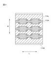
- a second internal electrode layer pattern 115B which becomes the second internal electrode layer 15B is formed from a conductive paste on a second ceramic green sheet 114B which becomes the dielectric layer 14c.
- the second internal electrode layer pattern 115B has a shape in which a plurality of second internal electrode layers 15B are continuous in the width direction W but discontinuous in the length direction L.
- the ceramic green sheet 114 is a strip-shaped sheet formed by forming a ceramic slurry containing ceramic powder, binder, and solvent onto a carrier film using a die coater, gravure coater, microgravure coater, etc.
- the first internal electrode layer pattern 115A and the second internal electrode layer pattern 115B are formed by printing, for example, screen printing, gravure printing, letterpress printing, etc.
- the ceramic paste 114a fills the entire portion of the first ceramic green sheet 114A where the first internal electrode layer pattern 115A is not arranged, and On both sides of the first internal electrode layer 15A in the longitudinal direction L, The extension regions 15Aw1 and 15Aw2 are arranged to overlap a range excluding a virtual region connecting the first extension region 15Aw1 and the second extension region 15Aw2, from a region corresponding to a part of the first end face C1 side of the first opposing portion 15Aa and the first transition region 15At1 overlapping with the first edge region 15Be1 of the second internal electrode layer 15B when viewed in a plane from the stacking direction T, and a region corresponding to a part of the second end face C2 side of the first opposing portion 15Aa and the second transition region 15At2 overlapping with the second edge region 15Be2 of the second internal electrode layer 15B when viewed in a plane from the stacking direction T.
- a ceramic paste 114b to become the dielectric layer 14b is applied onto the sheet on which the second internal electrode layer pattern 115B is formed on the second ceramic green sheet 114B shown in Fig. 8.
- the thickness of the dielectric layer 14b is 0.4 to 0.8 times the thickness of the dielectric layer 14c.
- the ceramic paste 114b fills the entire portion of the second ceramic green sheet 114B where the second internal electrode layer pattern 115B is not arranged, and is further arranged so as to overlap the portions corresponding to the first edge region 15Be1 and the second edge region 15Be2 on both side edges in the longitudinal direction L of the second opposing portion 15Ba of the second internal electrode layer pattern 115B.
- the multilayer ceramic capacitor 200 in which the first internal electrode layer 15A is connected to the first end surface external electrode 3a and the second internal electrode layer 15B is connected to the second end surface external electrode 3b can be used as a two-terminal capacitor.
Landscapes
- Engineering & Computer Science (AREA)
- Power Engineering (AREA)
- Manufacturing & Machinery (AREA)
- Microelectronics & Electronic Packaging (AREA)
- Chemical & Material Sciences (AREA)
- Ceramic Engineering (AREA)
- Inorganic Chemistry (AREA)
- Fixed Capacitors And Capacitor Manufacturing Machines (AREA)
- Ceramic Capacitors (AREA)
Priority Applications (4)
| Application Number | Priority Date | Filing Date | Title |
|---|---|---|---|
| KR1020257018700A KR20250102087A (ko) | 2022-12-28 | 2023-11-21 | 적층 세라믹 콘덴서 |
| JP2024567294A JPWO2024142679A1 (https=) | 2022-12-28 | 2023-11-21 | |
| CN202380089413.9A CN120380560A (zh) | 2022-12-28 | 2023-11-21 | 层叠陶瓷电容器 |
| US19/251,874 US20250329497A1 (en) | 2022-12-28 | 2025-06-27 | Multilayer ceramic capacitor |
Applications Claiming Priority (2)
| Application Number | Priority Date | Filing Date | Title |
|---|---|---|---|
| JP2022212598 | 2022-12-28 | ||
| JP2022-212598 | 2022-12-28 |
Related Child Applications (1)
| Application Number | Title | Priority Date | Filing Date |
|---|---|---|---|
| US19/251,874 Continuation US20250329497A1 (en) | 2022-12-28 | 2025-06-27 | Multilayer ceramic capacitor |
Publications (1)
| Publication Number | Publication Date |
|---|---|
| WO2024142679A1 true WO2024142679A1 (ja) | 2024-07-04 |
Family
ID=91717197
Family Applications (1)
| Application Number | Title | Priority Date | Filing Date |
|---|---|---|---|
| PCT/JP2023/041870 Ceased WO2024142679A1 (ja) | 2022-12-28 | 2023-11-21 | 積層セラミックコンデンサ |
Country Status (5)
| Country | Link |
|---|---|
| US (1) | US20250329497A1 (https=) |
| JP (1) | JPWO2024142679A1 (https=) |
| KR (1) | KR20250102087A (https=) |
| CN (1) | CN120380560A (https=) |
| WO (1) | WO2024142679A1 (https=) |
Citations (5)
| Publication number | Priority date | Publication date | Assignee | Title |
|---|---|---|---|---|
| JP2004047536A (ja) * | 2002-07-09 | 2004-02-12 | Murata Mfg Co Ltd | 積層セラミックコンデンサ及びその製造方法 |
| JP2008294298A (ja) * | 2007-05-25 | 2008-12-04 | Murata Mfg Co Ltd | 電子部品 |
| JP2012099786A (ja) * | 2010-10-29 | 2012-05-24 | Samsung Electro-Mechanics Co Ltd | 積層型セラミックキャパシタ及びその製造方法 |
| JP2022053271A (ja) * | 2020-09-24 | 2022-04-05 | 株式会社村田製作所 | 積層セラミックコンデンサ |
| JP2022075191A (ja) * | 2020-11-06 | 2022-05-18 | 株式会社村田製作所 | 積層セラミックコンデンサ及び積層セラミックコンデンサの製造方法 |
Family Cites Families (1)
| Publication number | Priority date | Publication date | Assignee | Title |
|---|---|---|---|---|
| JP3885962B2 (ja) | 2003-05-21 | 2007-02-28 | Tdk株式会社 | セラミック電子部品の製造方法 |
-
2023
- 2023-11-21 WO PCT/JP2023/041870 patent/WO2024142679A1/ja not_active Ceased
- 2023-11-21 KR KR1020257018700A patent/KR20250102087A/ko active Pending
- 2023-11-21 JP JP2024567294A patent/JPWO2024142679A1/ja active Pending
- 2023-11-21 CN CN202380089413.9A patent/CN120380560A/zh active Pending
-
2025
- 2025-06-27 US US19/251,874 patent/US20250329497A1/en active Pending
Patent Citations (5)
| Publication number | Priority date | Publication date | Assignee | Title |
|---|---|---|---|---|
| JP2004047536A (ja) * | 2002-07-09 | 2004-02-12 | Murata Mfg Co Ltd | 積層セラミックコンデンサ及びその製造方法 |
| JP2008294298A (ja) * | 2007-05-25 | 2008-12-04 | Murata Mfg Co Ltd | 電子部品 |
| JP2012099786A (ja) * | 2010-10-29 | 2012-05-24 | Samsung Electro-Mechanics Co Ltd | 積層型セラミックキャパシタ及びその製造方法 |
| JP2022053271A (ja) * | 2020-09-24 | 2022-04-05 | 株式会社村田製作所 | 積層セラミックコンデンサ |
| JP2022075191A (ja) * | 2020-11-06 | 2022-05-18 | 株式会社村田製作所 | 積層セラミックコンデンサ及び積層セラミックコンデンサの製造方法 |
Also Published As
| Publication number | Publication date |
|---|---|
| CN120380560A (zh) | 2025-07-25 |
| US20250329497A1 (en) | 2025-10-23 |
| JPWO2024142679A1 (https=) | 2024-07-04 |
| KR20250102087A (ko) | 2025-07-04 |
Similar Documents
| Publication | Publication Date | Title |
|---|---|---|
| JP7536620B2 (ja) | セラミック電子部品、実装基板およびセラミック電子部品の製造方法 | |
| JP2024099773A (ja) | 電子部品、回路基板および電子部品の製造方法 | |
| US10186381B2 (en) | Composite electronic component and resistance element | |
| CN115881434B (zh) | 层叠陶瓷电容器 | |
| JP2022077451A (ja) | 積層セラミックコンデンサ | |
| WO2024142679A1 (ja) | 積層セラミックコンデンサ | |
| WO2023210465A1 (ja) | 積層セラミックコンデンサ及び積層セラミックコンデンサの実装方法 | |
| JP2024162476A (ja) | 積層セラミックコンデンサ | |
| JP7852745B2 (ja) | 積層セラミックコンデンサ | |
| JP7751261B2 (ja) | 積層セラミックコンデンサ | |
| WO2024142672A1 (ja) | 積層セラミックコンデンサ | |
| JP2022166463A (ja) | セラミック電子部品および実装基板 | |
| US20260128216A1 (en) | Multilayer ceramic electronic component | |
| US20230343521A1 (en) | Multilayer ceramic capacitor and mounting structure of multilayer ceramic capacitor | |
| US20250166926A1 (en) | Multilayer ceramic electronic component | |
| WO2025150229A1 (ja) | 積層セラミックコンデンサ | |
| WO2025052706A1 (ja) | 積層セラミック電子部品 | |
| JP2024022341A (ja) | 積層セラミックコンデンサおよび積層セラミックコンデンサの実装構造 | |
| WO2025018007A1 (ja) | 積層セラミック電子部品 | |
| WO2024247445A1 (ja) | 積層セラミックコンデンサ | |
| CN120600530A (zh) | 层叠陶瓷电子部件 | |
| WO2025018005A1 (ja) | 積層セラミック電子部品 | |
| CN121532842A (zh) | 层叠陶瓷电容器 | |
| WO2025121052A1 (ja) | 電子部品の実装構造 | |
| WO2025004486A1 (ja) | 積層セラミックコンデンサ |
Legal Events
| Date | Code | Title | Description |
|---|---|---|---|
| 121 | Ep: the epo has been informed by wipo that ep was designated in this application |
Ref document number: 23911461 Country of ref document: EP Kind code of ref document: A1 |
|
| ENP | Entry into the national phase |
Ref document number: 20257018700 Country of ref document: KR Kind code of ref document: A |
|
| WWE | Wipo information: entry into national phase |
Ref document number: 1020257018700 Country of ref document: KR |
|
| WWE | Wipo information: entry into national phase |
Ref document number: 2024567294 Country of ref document: JP |
|
| WWE | Wipo information: entry into national phase |
Ref document number: 202380089413.9 Country of ref document: CN |
|
| WWP | Wipo information: published in national office |
Ref document number: 1020257018700 Country of ref document: KR |
|
| WWP | Wipo information: published in national office |
Ref document number: 202380089413.9 Country of ref document: CN |
|
| NENP | Non-entry into the national phase |
Ref country code: DE |
|
| 122 | Ep: pct application non-entry in european phase |
Ref document number: 23911461 Country of ref document: EP Kind code of ref document: A1 |