WO2024136365A1 - 포지티브형 감광성 수지 조성물 및 이를 포함하는 전자 소자 - Google Patents
포지티브형 감광성 수지 조성물 및 이를 포함하는 전자 소자 Download PDFInfo
- Publication number
- WO2024136365A1 WO2024136365A1 PCT/KR2023/020862 KR2023020862W WO2024136365A1 WO 2024136365 A1 WO2024136365 A1 WO 2024136365A1 KR 2023020862 W KR2023020862 W KR 2023020862W WO 2024136365 A1 WO2024136365 A1 WO 2024136365A1
- Authority
- WO
- WIPO (PCT)
- Prior art keywords
- group
- formula
- photosensitive resin
- resin composition
- positive
- Prior art date
- Legal status (The legal status is an assumption and is not a legal conclusion. Google has not performed a legal analysis and makes no representation as to the accuracy of the status listed.)
- Ceased
Links
Images


Classifications
-
- G—PHYSICS
- G03—PHOTOGRAPHY; CINEMATOGRAPHY; ANALOGOUS TECHNIQUES USING WAVES OTHER THAN OPTICAL WAVES; ELECTROGRAPHY; HOLOGRAPHY
- G03F—PHOTOMECHANICAL PRODUCTION OF TEXTURED OR PATTERNED SURFACES, e.g. FOR PRINTING, FOR PROCESSING OF SEMICONDUCTOR DEVICES; MATERIALS THEREFOR; ORIGINALS THEREFOR; APPARATUS SPECIALLY ADAPTED THEREFOR
- G03F7/00—Photomechanical, e.g. photolithographic, production of textured or patterned surfaces, e.g. printing surfaces; Materials therefor, e.g. comprising photoresists; Apparatus specially adapted therefor
- G03F7/004—Photosensitive materials
-
- G—PHYSICS
- G03—PHOTOGRAPHY; CINEMATOGRAPHY; ANALOGOUS TECHNIQUES USING WAVES OTHER THAN OPTICAL WAVES; ELECTROGRAPHY; HOLOGRAPHY
- G03F—PHOTOMECHANICAL PRODUCTION OF TEXTURED OR PATTERNED SURFACES, e.g. FOR PRINTING, FOR PROCESSING OF SEMICONDUCTOR DEVICES; MATERIALS THEREFOR; ORIGINALS THEREFOR; APPARATUS SPECIALLY ADAPTED THEREFOR
- G03F7/00—Photomechanical, e.g. photolithographic, production of textured or patterned surfaces, e.g. printing surfaces; Materials therefor, e.g. comprising photoresists; Apparatus specially adapted therefor
- G03F7/004—Photosensitive materials
- G03F7/016—Diazonium salts or compounds
-
- G—PHYSICS
- G03—PHOTOGRAPHY; CINEMATOGRAPHY; ANALOGOUS TECHNIQUES USING WAVES OTHER THAN OPTICAL WAVES; ELECTROGRAPHY; HOLOGRAPHY
- G03F—PHOTOMECHANICAL PRODUCTION OF TEXTURED OR PATTERNED SURFACES, e.g. FOR PRINTING, FOR PROCESSING OF SEMICONDUCTOR DEVICES; MATERIALS THEREFOR; ORIGINALS THEREFOR; APPARATUS SPECIALLY ADAPTED THEREFOR
- G03F7/00—Photomechanical, e.g. photolithographic, production of textured or patterned surfaces, e.g. printing surfaces; Materials therefor, e.g. comprising photoresists; Apparatus specially adapted therefor
- G03F7/004—Photosensitive materials
- G03F7/016—Diazonium salts or compounds
- G03F7/0163—Non ionic diazonium compounds, e.g. diazosulphonates; Precursors thereof, e.g. triazenes
-
- G—PHYSICS
- G03—PHOTOGRAPHY; CINEMATOGRAPHY; ANALOGOUS TECHNIQUES USING WAVES OTHER THAN OPTICAL WAVES; ELECTROGRAPHY; HOLOGRAPHY
- G03F—PHOTOMECHANICAL PRODUCTION OF TEXTURED OR PATTERNED SURFACES, e.g. FOR PRINTING, FOR PROCESSING OF SEMICONDUCTOR DEVICES; MATERIALS THEREFOR; ORIGINALS THEREFOR; APPARATUS SPECIALLY ADAPTED THEREFOR
- G03F7/00—Photomechanical, e.g. photolithographic, production of textured or patterned surfaces, e.g. printing surfaces; Materials therefor, e.g. comprising photoresists; Apparatus specially adapted therefor
- G03F7/004—Photosensitive materials
- G03F7/016—Diazonium salts or compounds
- G03F7/021—Macromolecular diazonium compounds; Macromolecular additives, e.g. binders
-
- G—PHYSICS
- G03—PHOTOGRAPHY; CINEMATOGRAPHY; ANALOGOUS TECHNIQUES USING WAVES OTHER THAN OPTICAL WAVES; ELECTROGRAPHY; HOLOGRAPHY
- G03F—PHOTOMECHANICAL PRODUCTION OF TEXTURED OR PATTERNED SURFACES, e.g. FOR PRINTING, FOR PROCESSING OF SEMICONDUCTOR DEVICES; MATERIALS THEREFOR; ORIGINALS THEREFOR; APPARATUS SPECIALLY ADAPTED THEREFOR
- G03F7/00—Photomechanical, e.g. photolithographic, production of textured or patterned surfaces, e.g. printing surfaces; Materials therefor, e.g. comprising photoresists; Apparatus specially adapted therefor
- G03F7/004—Photosensitive materials
- G03F7/016—Diazonium salts or compounds
- G03F7/021—Macromolecular diazonium compounds; Macromolecular additives, e.g. binders
- G03F7/0212—Macromolecular diazonium compounds; Macromolecular additives, e.g. binders characterised by the polymeric binder or the macromolecular additives other than the diazo resins or the polymeric diazonium compounds
- G03F7/0217—Polyurethanes; Epoxy resins
-
- G—PHYSICS
- G03—PHOTOGRAPHY; CINEMATOGRAPHY; ANALOGOUS TECHNIQUES USING WAVES OTHER THAN OPTICAL WAVES; ELECTROGRAPHY; HOLOGRAPHY
- G03F—PHOTOMECHANICAL PRODUCTION OF TEXTURED OR PATTERNED SURFACES, e.g. FOR PRINTING, FOR PROCESSING OF SEMICONDUCTOR DEVICES; MATERIALS THEREFOR; ORIGINALS THEREFOR; APPARATUS SPECIALLY ADAPTED THEREFOR
- G03F7/00—Photomechanical, e.g. photolithographic, production of textured or patterned surfaces, e.g. printing surfaces; Materials therefor, e.g. comprising photoresists; Apparatus specially adapted therefor
- G03F7/004—Photosensitive materials
- G03F7/039—Macromolecular compounds which are photodegradable, e.g. positive electron resists
Definitions
- the present invention relates to a positive photosensitive resin composition and an electronic device containing the same. More specifically, it relates to a positive photosensitive resin composition with excellent solubility and no swelling during development and an electronic device containing the same.
- Photosensitive resin is a representative functional polymer material that has been used in the production of various precision electronic and information industrial products, and is currently being used importantly in the high-tech industry, especially in the production of semiconductors and displays.
- photosensitive resin refers to a polymer compound in which a chemical change in the molecular structure occurs within a short period of time due to light irradiation, resulting in changes in physical properties such as solubility in a specific solvent, coloring, and curing.
- micro-precision processing is possible, energy and raw materials can be greatly reduced compared to thermal reaction processes, and work can be performed quickly and accurately in a small installation space, so it can be used in advanced printing fields, semiconductor production, and display production. It is widely used in various precision electronic and information industries, such as photocurable surface coating materials.
- photosensitive resins can be broadly divided into negative type and positive type.
- the negative type photosensitive resin is a type in which the light-irradiated portion is insoluble in the developer
- positive type photosensitive resin is a type in which the light-irradiated portion is solubilized in the developer. am.
- the polymer used in positive photosensitive resin requires that after selective exposure, the exposed portion must have low or no solubility in the developer, and the unexposed portion must have high solubility in the developer. These requirements are required for precision electronics . In the information industry, there is an increasing need to be able to form extremely fine patterns.
- the present invention seeks to provide a positive photosensitive resin composition containing polyimide of a closed ring structure with excellent solubility and no swelling phenomenon during the development process when forming a pattern using the positive photosensitive composition.
- the present invention is to provide an electronic device including an organic insulating film or a photosensitive pattern formed from the positive photosensitive resin composition.
- An exemplary embodiment of the present specification includes a polyimide resin represented by the following formula (1); A thermosetting agent containing an epoxy ring; and a development control agent of the following formula (3).
- X1 and X2 are the same or different from each other and are each independently a tetravalent organic group
- Y is a divalent to tetravalent organic group
- R 3 to R 6 are the same as or different from each other, and are each independently hydrogen; Or a substituted or unsubstituted alkyl group,
- n 1 , m 2 , k 1 and k 2 are the same as or different from each other and are each independently 0 or 1, and 1 ⁇ m 1 +m 2 +k 1 +k 2 ⁇ 2,
- Z is represented by the following formula 2-1, the following formula 2-2, or a combination thereof,
- the sum of the molar ratios of Y and Z is 1, the sum of the molar ratios of Z is 0.05 or more and 0.3 or less,
- n is a real number from 1 to 50
- m is a real number from 0 to 50
- R 7 and R 8 are the same as or different from each other and are each independently hydrogen; heavy hydrogen; hydroxyl group; It is an alkoxy or carboxy group,
- t is a real number from 1 to 4,
- s is a real number from 1 to 5
- L1 and L2 are the same or different from each other and are each independently a divalent or tetravalent organic group
- the sum of o and p is a real number between 2 and 100.
- another embodiment of the present invention provides an electronic device including an organic insulating film or a photosensitive pattern formed from the positive photosensitive resin composition.
- the resolution of the pattern is improved by improving the developability of the exposed area during development after selective exposure, and the polyimide main chain of Formula 1 is formed in the heat curing process. Flexibility can be improved by forming a crosslink with the carboxy group (-COOH) of the development regulator of Formula 3. This improves chemical resistance and mechanical properties, and enables low-temperature curing.
- an electronic device including an organic insulating film or photosensitive pattern with excellent performance formed from the positive photosensitive resin composition according to the present specification can be provided.
- Figure 1 shows an example of an organic insulating film for a semiconductor containing a photosensitive resin composition according to an exemplary embodiment of the present invention.
- Figure 2 shows an example of an organic insulating film for an organic light-emitting device containing a photosensitive resin composition according to an exemplary embodiment of the present invention.
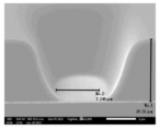
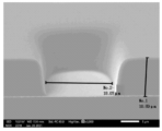
- FIG. 3 and 4 are photographs of a photosensitive pattern using a photosensitive resin composition according to an exemplary embodiment of the present invention.
- the aromatic (organic) group may be a C6 to C20 arylene group, and the aliphatic group may be a C1 to C20 alkylene group, or a C3 to C20 cycloalkylene group.
- the arylene group includes a phenylene group and the like.
- the halogen group may be F, Cl, Br, or I.
- substituted or unsubstituted refers to deuterium; halogen group; hydroxyl group; -COOH; Alkyl group; Cycloalkyl group; Aryl group; and is substituted with one or more substituents selected from the group containing heteroaryl groups or does not have any substituents.
- the alkyl group may be straight chain or branched, and the number of carbon atoms is not particularly limited, but is preferably 1 to 60. According to one embodiment, the carbon number of the alkyl group is 1 to 30. According to another embodiment, the carbon number of the alkyl group is 1 to 20. According to another embodiment, the carbon number of the alkyl group is 1 to 10. Specific examples of alkyl groups include methyl group, ethyl group, n-propyl group, isopropyl group, n-butyl group, isobutyl group, tert-butyl group, n-pentyl group, n-hexyl group, n-heptyl group, and n-oxyl group. There is a til group, etc., but it is not limited to these.
- the cycloalkyl group is not particularly limited, but preferably has 3 to 60 carbon atoms, and according to one embodiment, the cycloalkyl group has 3 to 30 carbon atoms. According to another embodiment, the carbon number of the cycloalkyl group is 3 to 20. According to another embodiment, the carbon number of the cycloalkyl group is 3 to 6. Specifically, it includes cyclopropyl group, cyclobutyl group, cyclopentyl group, cyclohexyl group, cycloheptyl group, cyclooctyl group, etc., but is not limited thereto.
- the aryl group is not particularly limited, but preferably has 6 to 60 carbon atoms and may be a monocyclic aryl group or a polycyclic aryl group. According to one embodiment, the aryl group has 6 to 30 carbon atoms. According to one embodiment, the aryl group has 6 to 20 carbon atoms.
- the aryl group may be a monocyclic aryl group, such as a phenyl group, biphenyl group, or terphenyl group, but is not limited thereto.
- the polycyclic aryl group may include a naphthyl group, anthracenyl group, indenyl group, phenanthrenyl group, pyrenyl group, perylenyl group, triphenyl group, chrysenyl group, fluorenyl group, etc., but is not limited thereto.
- the heterocyclic group is a heterocyclic group containing O, N, or S as a heteroatom, and the number of carbon atoms is not particularly limited, but has 2 to 30 carbon atoms, specifically 2 to 20 carbon atoms.
- heterocyclic groups include thiophene group, furan group, pyrrole group, imidazole group, thiazole group, oxazole group, oxadiazole group, triazole group, pyridyl group, bipyridyl group, triazine group, acridyl group, and pyridazine group.
- quinolinyl group isoquinoline group, indole group, carbazole group, benzoxazole group, benzoimidazole group, benzothiazole group, benzocarbazole group, benzothiophene group, dibenzothiophene group, benzofuranyl group, dibenzofuran There are others, but it is not limited to these.
- the heterocyclic group may be an aliphatic or aromatic ring group.
- heterocyclic group described above can be applied, except that the heteroaryl group is aromatic.
- An exemplary embodiment of the present invention includes a polyimide resin represented by the following formula (1); A thermosetting agent containing an epoxy ring; and a development control agent of the following formula (3).
- X1 and X2 are the same or different from each other and are each independently a tetravalent organic group
- Y is a divalent to tetravalent organic group
- R 3 to R 6 are the same as or different from each other, and are each independently hydrogen; Or a substituted or unsubstituted alkyl group,
- n 1 , m 2 , k 1 and k 2 are the same as or different from each other and are each independently 0 or 1, and 1 ⁇ m 1 +m 2 +k 1 +k 2 ⁇ 2,
- Z is represented by the following formula 2-1, the following formula 2-2, or a combination thereof,
- the sum of the molar ratios of Y and Z is 1, the sum of the molar ratios of Z is 0.05 or more and 0.3 or less,
- n is a real number from 1 to 50
- m is a real number from 0 to 50
- R 7 and R 8 are the same as or different from each other and are each independently hydrogen; heavy hydrogen; hydroxyl group; It is an alkoxy or carboxy group,
- t is a real number from 1 to 4,
- s is a real number from 1 to 5
- L1 and L2 are the same or different from each other and are each independently a divalent or tetravalent organic group
- the sum of o and p is a real number between 2 and 100
- the present inventors have found that the terminal structure (Z) of the polyimide resin having the structure of Formula 1 and the carboxyl group (-COOH) of the development regulator of Formula 3 form a cross linker, providing the effect of improving flexibility, and as a result It was confirmed through experiments that not only the mechanical properties were improved, but also the chemical resistance was improved and ultra-fine patterns could be easily formed, and the invention was completed based on this.
- the positive photosensitive resin composition does not use a polyimide precursor that requires a high-temperature heat curing process (imidization process), but uses a polyimide resin that can be solution processed at low temperature, thereby replacing the high-temperature imidization process. there is.
- At least one of X1 and X2 may be a tetravalent aromatic organic group.
- At least one of X1 and X2 may be a tetravalent aliphatic organic group.
- At least one of X1 and X2 may be a tetravalent organic group in which an aromatic group and an aliphatic group are connected to each other.
- both X1 and X2 may be tetravalent aromatic organic groups.
- both X1 and X2 may be tetravalent aliphatic organic groups.
- both X1 and X2 may be tetravalent organic groups in which an aromatic group and an aliphatic group are connected to each other.
- each carbonyl group may be a portion connected to another structure (specifically, each carbonyl group) in Formula 1 above.
- At least one of X1 and X2 may be selected from the group consisting of the following structures.
- At least one of X1 and X2 may be selected from the group consisting of the following structures.
- Y in Formula 1 is selected from the group consisting of a divalent to tetravalent aromatic organic group, a divalent to tetravalent aliphatic organic group, and a divalent to tetravalent organic group in which an aromatic group and an aliphatic group are linked to each other. It can be.
- Y may be a divalent to tetravalent aromatic organic group.
- Y may be a divalent to tetravalent aliphatic organic group.
- Y may be a divalent to tetravalent organic group in which an aromatic group and an aliphatic group are connected to each other.
- Y may be selected from the group consisting of the following structures.
- A is a divalent organic group
- N in Formula 1 may be a portion connected to another structure in Formula 1 (specifically, N in Formula 1).
- either -OH in the above structure may be replaced with -COOH.
- Y may be any one of the following structures.
- A may be selected from the group consisting of the following structures.
- A may be any one of the following structures.
- A may have the following structure.
- R 3 to R 6 in Formula 1 are the same as or different from each other, and are each independently hydrogen; Alternatively, it may be a substituted or unsubstituted alkyl group having 1 to 60 carbon atoms.
- R 3 to R 6 are the same as or different from each other, and are each independently hydrogen; Alternatively, it may be a substituted or unsubstituted alkyl group having 1 to 40 carbon atoms.
- R 3 to R 6 are the same as or different from each other, and are each independently hydrogen; Alternatively, it may be a substituted or unsubstituted alkyl group having 1 to 20 carbon atoms.
- R 3 to R 6 are the same as or different from each other, and are each independently hydrogen; Or, it may be an unsubstituted alkyl group having 1 to 20 carbon atoms.
- R 3 to R 6 are the same as or different from each other, and may each independently be hydrogen.
- R 7 and R 8 of Formulas 2-1 and 2-2 are the same as or different from each other, and are each independently hydrogen; heavy hydrogen; hydroxyl group; It may be an alkoxy group or a carboxy group, and at least one may be a hydroxy group or a carboxy group.
- R 7 and R 8 of Formulas 2-1 and 2-2 are the same as or different from each other, and are each independently hydrogen; heavy hydrogen; hydroxyl group; or a carboxyl group, and at least one may be a hydroxy group or a carboxyl group.
- R 7 and R 8 are the same as or different from each other, and are each independently hydrogen; hydroxyl group; or a carboxyl group, and at least one may be a hydroxy group or a carboxyl group.
- Q in Formula 3 may be CH 2 or S.
- Q in Formula 3 may be CH 2 .
- the polyimide resin has the effect of reducing light blocking of the 365 nm wavelength by the polyimide resin during the exposure process, thereby improving fine processing and sensitivity.
- the polyimide resin may further include a structure represented by the following formula E as an end group.
- Re1 is hydrogen; Or a substituted or unsubstituted alkyl group,
- re1 is a real number from 0 to 4, and if re1 is 2 or more, Re1 is the same or different,
- Re1 is hydrogen; Or it is a substituted or unsubstituted alkyl group having 1 to 60 carbon atoms.
- Re1 is hydrogen; Or it is a substituted or unsubstituted alkyl group having 1 to 40 carbon atoms.
- Re1 is hydrogen; Or it is a substituted or unsubstituted alkyl group having 1 to 20 carbon atoms.
- Re1 is hydrogen
- the polyimide resin may have a weight average molecular weight of 5,000 g/mol to 200,000 g/mol.
- the weight average molecular weight is less than 5,000, it may be difficult to implement the desired coating properties and mechanical properties when applying the polyimide copolymer, and if it is more than 200,000, the solubility in the developer may be low, making it difficult to apply it as a photosensitive material. .
- the weight average molecular weight is one of the average molecular weights that are used as a standard for the molecular weight of certain polymer materials whose molecular weight is not uniform. It is a value obtained by averaging the molecular weights of the component molecular species of a polymer compound with a molecular weight distribution by weight fraction.
- the weight average molecular weight may be a value measured by gel permeation chromatography, that is, GPC.
- thermosetting agent may include two or more epoxy rings.
- thermosetting agent may include additional functional groups such as an aromatic ring, an amine group, and an ether group in addition to two or more epoxy rings.
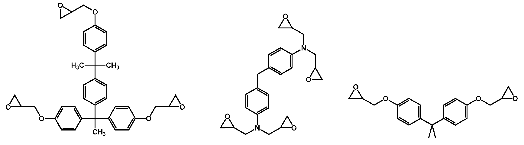
- thermosetting agent may have the following structure, but is not limited thereto.
- a photosensitizer may further include a surfactant and a solvent, but is not limited thereto.
- the surfactant is a silicone-based surfactant or a fluorine-based surfactant.
- the silicone-based surfactant is BYK-077, BYK-085, BYK-300, BYK-301, BYK-302, BYK-306, BYK-307 manufactured by BYK-Chemie.
- BYK-310, BYK-320, BYK-322, BYK-323, BYK-325, BYK-330, BYK-331, BYK-333, BYK-335, BYK-341, BYK-344, BYK-345, BYK -346, BYK-348, BYK-354, BYK-355, BYK-356, BYK-358, BYK-361, BYK-370, BYK-371, BYK-375, BYK-380, BYK-390, etc. are available.
- Fluorine-based surfactants include F-114, F-177, F-410, F-411, F-450, F-493, F-494, F-443, and F-444 from DIC (DaiNippon Ink & Chemicals). , F-445, F-446, F-470, F-471, F-472SF, F-474, F-475, F-477, F-478, F-479, F-480SF, F-482, F -483, F-484, F-486, F-487, F-172D, MCF-350SF, TF-1025SF, TF-1117SF, TF-1026SF, TF-1128, TF-1127, TF-1129, TF-1126 , TF-1130, TF-1116SF, TF-1131, TF1132, TF1027SF, TF-1441, TF-1442, etc. can be used, but are not limited to these.
- the solvent any compound known in the technical field to which the present invention pertains to enable the formation of a photosensitive resin composition may be used without particular limitation.
- the solvent may be one or more compounds selected from the group consisting of esters, ethers, ketones, aromatic hydrocarbons, and sulfoxides.
- the ester solvents include ethyl acetate, n-butyl acetate, isobutyl acetate, amyl formate, isoamyl acetate, isobutyl acetate, butyl propionate, isopropyl butyrate, ethyl butyrate, butyl butyrate, methyl lactate, ethyl lactate, gamma- Butyrolactone, epsilon-caprolactone, delta-valerolactone, alkyl oxyacetate (e.g. methyl oxyacetate, ethyl oxyacetate, butyl oxyacetate (e.g.
- 3-oxypropionic acid alkyl esters e.g., methyl 3-oxypropionate, ethyl 3-oxypropionate, etc. (e.g., methyl 3-methoxypropionate, 3 -Ethyl methoxypropionate, methyl 3-ethoxypropionate, ethyl 3-ethoxypropionate, etc.
- 2-oxypropionate alkyl esters e.g.
- methyl 2-oxypropionate, ethyl 2-oxypropionate, propyl 2-oxypropionate) e.g., methyl 2-methoxypropionate, ethyl 2-methoxypropionate, propyl 2-methoxypropionate, methyl 2-ethoxypropionate, ethyl 2-ethoxypropionate
- 2-oxy-2-methyl Methyl propionate and 2-oxy-2-methylethylpropionate e.g., methyl 2-methoxy-2-methylpropionate, ethyl 2-ethoxy-2-methylpropionate, etc.
- methyl pyruvate, ethyl pyruvate, propyl pyruvate It may be methyl acetoacetate, ethyl acetoacetate, methyl 2-oxobutanoate, ethyl 2-oxobutanoate, etc.
- the ether solvents include diethylene glycol dimethyl ether, tetrahydrofuran, ethylene glycol monomethyl ether, ethylene glycol monoethyl ether, methyl cellosolve acetate, ethyl cellosolve acetate, Ethylene glycol monomethyl ether, diethylene glycol monoethyl ether, diethylene glycol monobutyl ether, propylene glycol monomethyl ether, propylene glycol monomethyl ether acetate, propylene glycol It may be lycol monoethyl ether acetate, propylene glycol monopropyl ether acetate, etc.
- the ketone solvent may be methyl ethyl ketone, cyclohexanone, cyclopentanone, 2-heptanone, 3-heptanone, N-methyl-2-pyrrolidone, etc.
- the aromatic hydrocarbon solvent may be toluene, xylene, anisole, limonene, etc.
- the sulfoxide-based solvent may be dimethyl sulfoxide or the like.
- the positive photosensitive resin composition may further include additives known in the art depending on its intended use.
- the positive photosensitive resin composition may further include an adhesion promoter, an antifoaming agent, a leveling agent, an anti-gel agent, or a mixture thereof.
- a silane coupling agent having a functional group such as epoxy, carboxyl, or isocyanate can be used, and specific examples thereof include trimethoxysilyl benzoic acid, triethoxysilyl benzoic acid, and gamma.
- This adhesion promoter may be included in an amount of 0.1 to 10 parts by weight based on 100 parts by weight of the polyimide resin.
- the surfactant may be used without any restrictions as long as it is known to be used in photosensitive resin compositions, but it is preferable to use a fluorine-based surfactant or a silicone-based surfactant. These surfactants may be included in an amount of 0.1 to 5 parts by weight based on 100 parts by weight of the polyimide resin.
- the photosensitizer may include one or more diazonaphthoquinone structures.
- the photosensitizer with a diazonaphthoquinone structure has the property of inhibiting development with a developer by hydrogen bonding with phenol in the Bis-APAF diamine of the polyimide chain in the non-exposed area, while in the exposed area
- the photosensitizer of the diazonaphthoquinone structure is released in the form of N 2 and absorbs moisture around the area, changing into -COOH.
- the -COOH causes a faster developing speed with the developer than the unexposed area, so no Developability for miners can be further improved.
- the polyimide resin may include one or two or more types of polyimide resin.
- the above-mentioned polyimide resin can be used to produce one type of polyimide (example of the polyimide of Chemical Formula 1) using a dianhydride compound and a diamine compound.
- examples of polyimides materials and polymerization methods known in the art can be used.
- Another embodiment of the present invention provides an electronic device including an organic insulating film or a photosensitive pattern formed from the positive photosensitive resin composition described above.
- an electronic device wherein the organic insulating film includes an interlayer insulating film and a surface protective film, and the electronic device further includes a memory component.
- m 1 +m 2 +k 1 +k 2 is 1 or 2 and includes an OH or COOH group, it is advantageous to improve the surface condition when forming a photosensitive film.
- the organic insulating film or photosensitive pattern includes a polyimide of a specific structure and an acrylic compound containing one or more photocurable acrylic functional groups, and can be used as a substrate used in semiconductor devices, such as Au, Cu, Ni, Ti, etc. It can achieve high adhesion to metal substrates or inorganic substrates such as SiO2 or SiNx, while also having improved mechanical properties such as excellent heat resistance, insulation, or chemical resistance.
- the electronic devices include a plasma display panel (PDP), a touch panel, a light emitting diode (LED), an organic light emitting diode (OLED), and a liquid crystal display (LCD). , a thin film transistor liquid crystal display (LCD-TFT), a cathode ray tube (CRT), and a semiconductor, but is not limited thereto.
- PDP plasma display panel
- touch panel a touch panel
- LED light emitting diode
- OLED organic light emitting diode
- LCD liquid crystal display
- LCD-TFT thin film transistor liquid crystal display
- CRT cathode ray tube
- semiconductor but is not limited thereto.
- an electronic device including an organic insulating film or photosensitive pattern formed from the positive photosensitive resin composition can realize excellent performance such as high resolution and high sensitivity, and exhibit excellent film properties and high mechanical properties, as well as excellent heat resistance properties. For example, even when used for a long time or exposed to high temperature conditions for a long time, the adhesion of the organic insulating film or photosensitive pattern is not deteriorated and can be maintained firmly.
- Figure 1 shows an example of an organic insulating film for a semiconductor containing a photosensitive resin composition according to an exemplary embodiment of the present invention.
- the positive photosensitive resin composition according to an embodiment of the present invention is coated on a silicon wafer 1 and then exposed to form a first photosensitive pattern (referred to as PID1) 2, and a pad is in contact with this pattern.
- PID1 a first photosensitive pattern
- a pad is in contact with this pattern.
- a pad e.g. Cu pad
- a solder ball (4) is partially provided on the top of the pad.
- This PID1(2) can be used as an organic insulating film corresponding to the outermost layer of semiconductor packaging materials.
- FIG. 2 shows an example of an organic insulating film for an organic light-emitting device containing a photosensitive resin composition according to an exemplary embodiment of the present invention.
- a substrate 6 e.g., TFT glass or TFT plastic (here, TFT refers to a thin film transistor) is formed with a positive photosensitive resin composition according to an embodiment of the present invention.
- a first photosensitive pattern (referred to as a redistributed layer (RDL)) 7 is provided, and a pad 8 (eg, Ag pad) is provided in contact with this pattern.
- RDL redistributed layer
- a second photosensitive pattern (referred to as PDL (Pixel diffine layer)) 9 is formed using a negative photosensitive resin composition according to an embodiment of the present invention.
- the PDL 9 emits organic light. It can be used as an organic insulating film for devices.
- Figure 4 shows a 15 um square pattern and a thickness of 10 um
- Figure 3 shows a 5 um hole pattern and a thickness of 8 um.
- the organic insulating film may include various insulating films of a semiconductor device, for example, an interlayer insulating film, a surface protective film, a substrate electrode protective layer, a buffer coat film, or a passivation film.
- the electrical element may include various components of a semiconductor device.
- the interlayer insulating film and surface protective film are not particularly limited, and those commonly used in the art may be employed.
- the memory components are not particularly limited, and those commonly used in the art may be employed.
- the organic insulating film or photosensitive pattern includes the steps of applying the positive photosensitive resin composition on a support substrate and drying it to form a resin film; exposing the resin film to light; It may be formed through developing the exposed resin film with a developer and heat-treating the developed photosensitive resin film.
- a patterned photosensitive resin film can be easily formed on a substrate such as glass or silicon wafer.
- the method of applying the positive photosensitive resin composition is spin coating. coating, bar coating, screen printing, etc. can be used.
- Support substrates that can be used in the process of forming the photosensitive resin film can be used without particular limitations as long as they are known to be commonly used in the electronic communication field or semiconductor field. Specific examples include silicon wafers, glass substrates, metal substrates, ceramic substrates, A polymer substrate, etc. can be mentioned.
- a prebaked film can be formed by prebaking at 50°C to 150°C for 1 to 20 minutes to volatilize the solvent. If the drying temperature is too low, the amount of remaining solvent may become too large, resulting in film loss in the exposed area during development, which may lower the remaining film. If the drying temperature is too high, the curing reaction may be accelerated and the unexposed area may not be developed. there is.
- ultraviolet rays or visible light with a wavelength of 200 nm to 500 nm can be irradiated using a photomask on which the pattern to be processed is formed, and the exposure amount during irradiation is preferably 10 mJ/cm2 to 4,000 mJ/cm2.
- the exposure time is also not particularly limited and can be appropriately changed depending on the exposure device used, the wavelength of the irradiation light, or the exposure amount. Specifically, the exposure time can be changed within the range of 1 second to 150 seconds.
- an alkaline aqueous developer known to be commonly used in the semiconductor or display production step can be used without any restrictions.
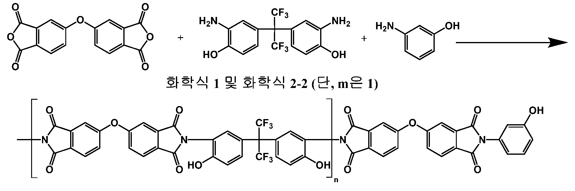
- n is a real number of 20 to 40, which indicates that the weight average molecular weight of the polymer is 15,000 g/mol.
- n is a real number of 20 to 40, which indicates that the weight average molecular weight of the polymer is 15,000 g/mol.
- a positive photosensitive resin composition was prepared using the components listed in Table 1 below. Specifically, a photosensitive resin composition was prepared including the prepared polyimide resin and each component listed in Table 1 below. Table 1 below is based on 100 parts by weight of the resin composition containing Synthesis Example 1 or 2, a photosensitive agent, a cross-linking agent, a surfactant, and a solvent.
- TPA529 (Miwon company)
- the photosensitive resin compositions of Examples 1 to 8 and Comparative Examples 1 to 3 were evaluated under the following process conditions, and the results are shown in Table 2 below. Specifically, the prepared photosensitive resin composition was applied on a Cu/Si wafer by spin coating. After soft baking at 120 o C for 120 seconds, exposure was performed at an appropriate exposure amount (i-line (365 nm)), and the development process was performed with a developer (2.38 wt% TMAH sol.) . Post bake was performed at 200°C for 1 hour each to confirm pattern properties. In addition, in order to measure the cured film temperature and mechanical properties, each prepared photosensitive resin composition was additionally coated on the Si wafer, subjected to full-scale exposure, and then soft-baked, followed by post-bake at 200°C for 1 hour. did.
- Resist evaluation conditions PrB 120 °C/120s, thickness 10 ⁇ m
- TMAH Tetramethylammonium hydroxide
- the minimum size of the pattern was measured through a SEM (Scanning Electron Microscope) of post-baked samples of each photosensitive resin composition produced at the same exposure dose.
- the cured film fully exposed on the previously prepared substrate was peeled from the substrate with an aqueous hydrogen fluoride solution, and then a cured film was manufactured.
- the Tg (glass transition temperature) and CTE (coefficient of thermal expansion) of the cured film were measured using TMA (Thermomechanical analysis) on an insulating film with a thickness of 10 ⁇ m dried in an oven, and the test was performed using a UTM (Universal Testing Machine) at room temperature and a speed of 5 cm/min. Elongation at break was measured.
- the polyimide resin according to the present specification and the photosensitive resin compositions of Examples 1 to 8 containing the same have high resolution pattern characteristics, and the cured film has excellent adhesion to the substrate.
- the cured film of the photosensitive resin composition has a relatively high elongation at break while maintaining a good Tg (glass transition temperature) and CTE (coefficient of thermal expansion), so it can secure excellent heat resistance and excellent mechanical properties, while at the same time maintaining a good Tg (glass transition temperature) and CTE (coefficient of thermal expansion). It was confirmed that pattern formation was possible.
Landscapes
- Physics & Mathematics (AREA)
- General Physics & Mathematics (AREA)
- Spectroscopy & Molecular Physics (AREA)
- Macromolecular Compounds Obtained By Forming Nitrogen-Containing Linkages In General (AREA)
- Materials For Photolithography (AREA)
- Epoxy Resins (AREA)
- Formation Of Insulating Films (AREA)
Abstract
Description







Claims (15)
- 하기 화학식 1로 표시되는 폴리이미드 수지; 에폭시 고리를 포함하는 열경화제; 및 하기 화학식 3의 현상 조절제를 포함하는 포지티브형 감광성 수지 조성물:[화학식 1]
 상기 화학식 1에 있어서,는 다른 구조에 결합되는 부분을 의미하고,
 X1 및 X2는 서로 같거나 상이하고, 각각 독립적으로 4가 유기기이고,Y는 2가 내지 4가 유기기이고,R3 내지 R6은 서로 같거나 상이하고, 각각 독립적으로 수소; 또는 치환 또는 비치환된 알킬기이고,m1, m2, k1 및 k2는 서로 같거나 상이하고, 각각 독립적으로 0 또는 1이며, 1 ≤ m1+m2+k1+k2 ≤ 2이고,Z는 하기 화학식 2-1, 하기 화학식 2-2, 또는 이들의 결합으로 표시되고,Y 및 Z의 몰(mol) 비율의 합이 1일 때, Z의 몰 비율의 합이 0.05 이상 0.3 이하이고,n은 1 내지 50의 실수이고,m은 0 내지 50의 실수이고,[화학식 2-1]
 [화학식 2-2]
 상기 화학식 2-1 및 화학식 2-2에 있어서,은 상기 화학식 1에 연결되는 부위이고,
 R7 및 R8은 서로 같거나 상이하고, 각각 독립적으로, 수소; 중수소; 히드록시기; 알콕시 또는 카르복시기이고,t는 1 내지 4의 실수이고,s는 1 내지 5의 실수이고,[화학식 3]
 상기 화학식 3에 있어서,L1 및 L2는 서로 같거나 상이하고, 각각 독립적으로 2가 또는 4가 유기기이고,Q는 CH2; O; C=O; S; 또는 N=N이고,o 및 p의 합은 2 내지 100의 실수이다.
 - 청구항 1에 있어서,X1 및 X2는 서로 같거나 상이하고, 각각 독립적으로 4가 방향족 유기기, 4가 지방족 유기기 및 방향족기와 지방족기가 서로 연결된 4가 유기기로 이루어진 군에서 선택되는 것인 포지티브형 감광성 수지 조성물.
- 청구항 1에 있어서,X1 및 X2는 서로 같거나 상이하고, 각각 독립적으로 하기 구조로 이루어진 군에서 선택되고,
 상기 구조에 있어서,는 상기 화학식 1에서 다른 구조에 연결되는 부위인 포지티브형 감광성 수지 조성물.
- 청구항 1에 있어서,Y는 2가 내지 4가 방향족 유기기, 2가 내지 4가 지방족 유기기 및 방향족기와 지방족기가 서로 연결된 2가 내지 4가 유기기로 이루어진 군으로부터 선택되는 것인 포지티브형 감광성 수지 조성물.
- 청구항 1에 있어서,Y는 하기 구조로 이루어진 군에서 선택되고,
 상기 구조에 있어서,A는 2가 유기기이고,는 상기 화학식 1에서 다른 구조에 연결되는 부위인 포지티브형 감광성 수지 조성물.
- 청구항 5에 있어서,A는 하기 구조로 이루어진 군에서 선택되는 것인 포지티브형 감광성 수지 조성물:
 상기 구조에 있어서,*는 다른 구조에 연결되는 부위이다.
 - 청구항 1에 있어서,R7 및 R8는 서로 같거나 상이하고, 각각 독립적으로 수소; 중수소; 히드록시기; 알콕시 또는 카르복시기이고, 적어도 하나는 히드록시기 또는 카르복시기인 포지티브형 감광성 수지 조성물.
- 청구항 1에 있어서,상기 폴리이미드 수지는 말단기로서 하기 화학식 E로 표시되는 구조를 더 포함하는 것인 포지티브형 감광성 수지 조성물:[화학식 E]
 상기 화학식 E에 있어서,*은 상기 화학식 1에 연결되는 부위이고,Re1은 수소; 또는 치환 또는 비치환된 알킬기이고,re1은 0 내지 4의 실수이고, re1이 2 이상인 경우 Re1은 서로 같거나 상이하고,Re는 수소이다.
 - 청구항 1에 있어서,상기 폴리이미드 수지는 중량평균 분자량이 5,000 g/mol 내지 200,000 g/mol인 것인 포지티브형 감광성 수지 조성물.
- 청구항 1에 있어서,상기 열경화제는 에폭시 고리를 2개 이상 포함하는 것인 포지티브형 감광성 수지 조성물.
- 청구항 1에 있어서,감광제; 계면활성제 및 용매를 더 포함하는 것인 포지티브형 감광성 수지 조성물.
- 청구항 11에 있어서,상기 감광제는 디아조나프토퀴논 구조를 1종 이상 포함하는 것인 포지티브형 감광성 수지 조성물.
- 청구항 1에 있어서,상기 폴리이미드 수지는 1종 또는 2종 이상의 폴리이미드 수지를 포함하는 것인 포지티브형 감광성 수지 조성물.
- 청구항 1 내지 13 중 어느 한 항에 따른 포지티브형 감광성 수지 조성물로부터 형성된 유기 절연막 또는 감광성 패턴을 포함하는 전자 소자.
- 청구항 14에 있어서,상기 유기 절연막은 층간 절연막 및 표면 보호막을 포함하고, 상기 전자 소자는 메모리 부품을 더 포함하는 것인 전자 소자.
Priority Applications (2)
| Application Number | Priority Date | Filing Date | Title |
|---|---|---|---|
| JP2025533417A JP2025538906A (ja) | 2022-12-23 | 2023-12-18 | ポジ型感光性樹脂組成物、およびこれを含む電子素子 |
| CN202380084158.9A CN120344915A (zh) | 2022-12-23 | 2023-12-18 | 正型光敏树脂组合物和包含其的电子装置 |
Applications Claiming Priority (2)
| Application Number | Priority Date | Filing Date | Title |
|---|---|---|---|
| KR1020220182702A KR102967275B1 (ko) | 2022-12-23 | 포지티브형 감광성 수지 조성물 및 이를 포함하는 전자 소자 | |
| KR10-2022-0182702 | 2022-12-23 |
Publications (1)
| Publication Number | Publication Date |
|---|---|
| WO2024136365A1 true WO2024136365A1 (ko) | 2024-06-27 |
Family
ID=91589316
Family Applications (1)
| Application Number | Title | Priority Date | Filing Date |
|---|---|---|---|
| PCT/KR2023/020862 Ceased WO2024136365A1 (ko) | 2022-12-23 | 2023-12-18 | 포지티브형 감광성 수지 조성물 및 이를 포함하는 전자 소자 |
Country Status (4)
| Country | Link |
|---|---|
| JP (1) | JP2025538906A (ko) |
| CN (1) | CN120344915A (ko) |
| TW (1) | TWI894741B (ko) |
| WO (1) | WO2024136365A1 (ko) |
Citations (5)
| Publication number | Priority date | Publication date | Assignee | Title |
|---|---|---|---|---|
| US5635563A (en) * | 1991-04-01 | 1997-06-03 | Tomoegawa Paper Co., Ltd. | Polyaniline derivatives and their production process |
| KR20080070924A (ko) * | 2007-01-29 | 2008-08-01 | 에스케이씨 주식회사 | 가교화된 폴리이미드 필름 및 이의 제조방법 |
| JP2011077251A (ja) * | 2009-09-30 | 2011-04-14 | Toray Ind Inc | ディスプレイ用部材および製造方法 |
| JP2011184508A (ja) * | 2010-03-05 | 2011-09-22 | Nippon Steel Chem Co Ltd | ポリイミド樹脂硬化膜及び光学補償部材 |
| KR20200010121A (ko) * | 2018-07-20 | 2020-01-30 | 주식회사 엘지화학 | 폴리이미드 수지 및 이를 포함하는 네거티브형 감광성 수지 조성물 |
-
2023
- 2023-12-18 WO PCT/KR2023/020862 patent/WO2024136365A1/ko not_active Ceased
- 2023-12-18 JP JP2025533417A patent/JP2025538906A/ja active Pending
- 2023-12-18 CN CN202380084158.9A patent/CN120344915A/zh active Pending
- 2023-12-21 TW TW112150112A patent/TWI894741B/zh active
Patent Citations (5)
| Publication number | Priority date | Publication date | Assignee | Title |
|---|---|---|---|---|
| US5635563A (en) * | 1991-04-01 | 1997-06-03 | Tomoegawa Paper Co., Ltd. | Polyaniline derivatives and their production process |
| KR20080070924A (ko) * | 2007-01-29 | 2008-08-01 | 에스케이씨 주식회사 | 가교화된 폴리이미드 필름 및 이의 제조방법 |
| JP2011077251A (ja) * | 2009-09-30 | 2011-04-14 | Toray Ind Inc | ディスプレイ用部材および製造方法 |
| JP2011184508A (ja) * | 2010-03-05 | 2011-09-22 | Nippon Steel Chem Co Ltd | ポリイミド樹脂硬化膜及び光学補償部材 |
| KR20200010121A (ko) * | 2018-07-20 | 2020-01-30 | 주식회사 엘지화학 | 폴리이미드 수지 및 이를 포함하는 네거티브형 감광성 수지 조성물 |
Also Published As
| Publication number | Publication date |
|---|---|
| TW202432710A (zh) | 2024-08-16 |
| KR20240100752A (ko) | 2024-07-02 |
| CN120344915A (zh) | 2025-07-18 |
| JP2025538906A (ja) | 2025-12-02 |
| TWI894741B (zh) | 2025-08-21 |
Similar Documents
| Publication | Publication Date | Title |
|---|---|---|
| WO2018159975A1 (ko) | 고분자 수지 화합물 및 이를 포함하는 블랙 뱅크용 감광성 수지 조성물 | |
| WO2020111522A1 (ko) | 감광성 수지 조성물, 필름 및 전자장치 | |
| WO2017119645A1 (ko) | 필름 터치 센서 및 이의 제조 방법 | |
| WO2017119761A1 (ko) | 필름 터치 센서 및 이의 제조 방법 | |
| WO2013129864A1 (ko) | 내열성이 우수한 화학증폭형 포지티브 감광형 고감도 유기절연막 조성물 및 이를 이용한 유기절연막의 형성방법 | |
| WO2019164157A1 (ko) | 화합물, 이를 포함하는 색재 조성물 및 이를 포함하는 수지 조성물 | |
| WO2022098199A1 (ko) | 감광성 수지 조성물, 이를 포함하는 감광재, 이를 포함하는 블랙 매트릭스 및 이를 포함하는 전자 소자 | |
| WO2022197110A1 (ko) | 포지티브형 감광성 수지 조성물, 절연막 및 이를 포함하는 표시장치 | |
| WO2017119764A1 (ko) | 필름 터치 센서 및 이의 제조 방법 | |
| WO2019132138A1 (ko) | 잔텐계 화합물 및 이를 포함하는 감광성 수지 조성물 | |
| WO2019107824A1 (ko) | 네거티브 감광성 수지 조성물, 이를 사용한 유기절연막을 갖는 전자장치 | |
| WO2020159174A1 (ko) | 폴리이미드계 수지 필름 및 이를 이용한 디스플레이 장치용 기판, 및 광학 장치 | |
| WO2022045737A1 (ko) | 포지티브형 감광성 수지 조성물 | |
| WO2022108046A1 (ko) | 폴리이미드 수지 필름, 이를 이용한 플렉서블 디스플레이 장치용 기판, 및 플렉서블 디스플레이 장치 | |
| WO2024091025A1 (ko) | 폴리이미드 수지, 이를 포함하는 네거티브형 감광성 수지 조성물 및 전자 소자 | |
| WO2020130261A1 (ko) | 가교제 화합물, 이를 포함하는 감광성 조성물, 및 이를 이용한 감광 재료 | |
| WO2024014689A1 (ko) | 감광성 수지 조성물, 경화막 및 이를 포함하는 표시장치 | |
| WO2023013923A1 (ko) | 포지티브형 감광성 수지 조성물 및 이를 포함하는 표시 장치 | |
| KR102931204B1 (ko) | 폴리이미드 수지, 이를 포함하는 네거티브형 감광성 수지 조성물 및 전자 소자 | |
| WO2020022670A1 (ko) | 바인더 수지, 감광성 수지 조성물, 감광재, 컬러필터 및 디스플레이 장치 | |
| WO2018147496A1 (ko) | 퍼릴렌 비스이미드계 화합물 및 이를 포함하는 염료 | |
| WO2023022472A1 (ko) | 감광성 수지 조성물 및 이를 포함하는 표시 장치 | |
| WO2022059971A1 (ko) | 플렉서블 디스플레이 장치 제조용 복합 기판, 이를 이용한 플렉서블 디스플레이 장치의 제조 방법, 및 플렉서블 디스플레이 장치용 적층체 | |
| KR102967275B1 (ko) | 포지티브형 감광성 수지 조성물 및 이를 포함하는 전자 소자 | |
| WO2020184972A1 (ko) | 폴리이미드 공중합체, 폴리이미드 공중합체의 제조방법, 이를 이용한 감광성 수지 조성물, 감광성 수지 필름 및 광학 장치 |
Legal Events
| Date | Code | Title | Description |
|---|---|---|---|
| 121 | Ep: the epo has been informed by wipo that ep was designated in this application |
Ref document number: 23907650 Country of ref document: EP Kind code of ref document: A1 |
|
| WWE | Wipo information: entry into national phase |
Ref document number: 202380084158.9 Country of ref document: CN |
|
| ENP | Entry into the national phase |
Ref document number: 2025533417 Country of ref document: JP Kind code of ref document: A |
|
| WWE | Wipo information: entry into national phase |
Ref document number: 2025533417 Country of ref document: JP |
|
| WWP | Wipo information: published in national office |
Ref document number: 202380084158.9 Country of ref document: CN |
|
| NENP | Non-entry into the national phase |
Ref country code: DE |
|
| 122 | Ep: pct application non-entry in european phase |
Ref document number: 23907650 Country of ref document: EP Kind code of ref document: A1 |