WO2024134748A1 - 基板搬送装置、部品実装機および基板搬送方法 - Google Patents
基板搬送装置、部品実装機および基板搬送方法 Download PDFInfo
- Publication number
- WO2024134748A1 WO2024134748A1 PCT/JP2022/046795 JP2022046795W WO2024134748A1 WO 2024134748 A1 WO2024134748 A1 WO 2024134748A1 JP 2022046795 W JP2022046795 W JP 2022046795W WO 2024134748 A1 WO2024134748 A1 WO 2024134748A1
- Authority
- WO
- WIPO (PCT)
- Prior art keywords
- substrate
- contact surface
- clamp member
- board
- transport
- Prior art date
- Legal status (The legal status is an assumption and is not a legal conclusion. Google has not performed a legal analysis and makes no representation as to the accuracy of the status listed.)
- Ceased
Links
Images







Classifications
-
- H—ELECTRICITY
- H05—ELECTRIC TECHNIQUES NOT OTHERWISE PROVIDED FOR
- H05K—PRINTED CIRCUITS; CASINGS OR CONSTRUCTIONAL DETAILS OF ELECTRIC APPARATUS; MANUFACTURE OF ASSEMBLAGES OF ELECTRICAL COMPONENTS
- H05K13/00—Apparatus or processes specially adapted for manufacturing or adjusting assemblages of electric components
- H05K13/0061—Tools for holding the circuit boards during processing; handling transport of printed circuit boards
Definitions
- This invention relates to a technology for transporting a substrate to perform processes such as component mounting, solder printing, or reflow on the substrate, and to a technology for dealing with charging of the substrate being transported.
- Patent Documents 1 and 2 disclose techniques for preventing the charging of circuit boards. That is, in Patent Document 1, in order to prevent the charging of the circuit boards transported on the component mounting line, the parts that come into contact with the circuit boards are grounded. In Patent Document 2, the surface resistivity of the antistatic material provided on the case that houses the circuit boards is set to 5.0 ⁇ 10 ⁇ 6 ( ⁇ / ⁇ ) or more, thereby preventing the pattern of the circuit board from being short-circuited by the antistatic material. In this specification, 10 ⁇ N (N is a natural number equal to or greater than 1) means 10 to the Nth power (10 N ).
- the board is transported in a predetermined transport direction in order to perform processes such as component mounting, solder printing, or reflow on the board.
- processes such as component mounting, solder printing, or reflow on the board.
- the board is transported in a predetermined transport direction in order to perform processes such as component mounting, solder printing, or reflow on the board.
- the board is transported in a predetermined transport direction in order to perform processes such as component mounting, solder printing, or reflow on the board.
- damage to components caused by charges flowing out of the board due to earthing has become a problem.
- damage to components could also be caused by charges flowing out of the board when the board comes into contact with metal members other than the earth.
- This invention was developed in consideration of the above problems, and aims to provide technology that makes it possible to suppress the charging of boards while slowing down the outflow of electric charge from the boards transported on a component mounting line.
- the substrate transport device comprises a substrate transport section that transports a substrate along a predetermined transport path, and a substrate transport auxiliary section that has a substrate contact surface and supports or guides the substrate by contacting the substrate contact surface with the substrate located on the transport path, the substrate contact surface being made of a material other than metal and being conductive.
- the substrate transport method includes a step of transporting a substrate along a predetermined transport path, and a step of supporting or guiding the substrate by contacting the substrate located on the transport path with a substrate contact surface, the substrate contact surface being made of a material other than metal and being conductive.
- a substrate is transported along a predetermined transport path. Furthermore, a substrate positioned on the transport path is supported or guided by a substrate contact surface that contacts the substrate. At this time, the substrate contact surface is conductive. Therefore, charges accumulated on the substrate flow out to the substrate contact surface that contacts the substrate, and the substrate is de-charged. Furthermore, because the substrate contact surface is not metal, the outflow of charges from the substrate to the substrate contact surface is gently suppressed. In this way, it is possible to suppress the charging of the substrate while easing the outflow of charges from the substrate transported on the component mounting line.
- the electrical resistance value of the substrate contact surface may be within a range that provides electrostatic dissipation. This makes it possible to suppress the electrostatic build-up of substrates while slowing down the outflow of electric charge from substrates transported on component mounting lines.
- the electrical resistance value of the board contact surface may be 1x10 ⁇ 4 ⁇ or more and less than 1x10 ⁇ 11 ⁇ .
- an electrical resistance value in the range of 1x10 ⁇ 4 ⁇ or more and less than 1x10 ⁇ 11 ⁇ is indicated as an electrical resistance value having electrostatic dissipation properties in IEC61340-5-1 (standard).
- the electrical resistance value of the board contact surface is less than 1x10 ⁇ 11 ⁇ , the charge accumulated on the board flows out to the board contact surface that contacts the board, and the board is de-charged.
- the electrical resistance value of the board contact surface is 1x10 ⁇ 4 ⁇ or more, the outflow of charge from the board to the board contact surface is gently suppressed. In this way, it is possible to suppress the charging of the board while easing the outflow of charge from the board transported on the component mounting line.
- the substrate transport device may also be configured so that the substrate transport auxiliary section has a base section on which a substrate contact surface is provided, and the hardness of the substrate contact surface is greater than the hardness of the base section. In this configuration, the durability of the substrate contact surface can be increased, and deterioration of the substrate contact surface due to contact with the substrate can be suppressed.
- the substrate may be a metal.
- the substrate contact surface may also be made of ceramics. Ceramics have high friction resistance and do not rust. This eliminates the need to replace the substrate contact surface for a long period of time, reducing the burden of maintenance.
- the substrate contact surface may also be made of coated ceramics.
- the ceramics can be applied to form a very thin layer, making it possible to form a substrate contact surface made of ceramics even for complex shapes.
- the substrate contact surface may also be formed by anodizing.
- Anodizing allows the substrate contact surface to be formed even for complex shapes, and because anodizing is inexpensive, it also reduces the cost of the substrate transport device.
- the substrate contact surface may also be formed by DLC processing.
- DLC processing can form a substrate contact surface with high precision even for complex shapes. It can also form a substrate contact surface with high hardness and wear resistance. Furthermore, it can form a substrate contact surface with a low coefficient of friction, so the substrate contact surface does not impede smooth transportation of the substrate.
- the substrate transport auxiliary unit may be configured so that it has a substrate guide disposed adjacent to the transport path, and the side end face of the substrate guide contacts the edge of the substrate as a substrate contact surface to guide the substrate.
- the side end face of the substrate guide comes into contact with the substrate frequently. Therefore, it is particularly preferable to configure the side end face of the substrate guide as a substrate contact surface that is made of a material other than metal and has electrical conductivity.
- the substrate transport auxiliary unit may also be configured to have a lower clamp member that faces the substrate supported by the substrate transport unit from below, and an upper clamp member that faces the substrate supported by the substrate transport unit from above, and to perform a clamping operation in which the substrate lifted from the substrate transport unit by the lower clamp member is clamped between the lower clamp member and the upper clamp member by raising the lower clamp member from the substrate transport unit, and a clamp release operation in which the clamping operation is released by lowering the lower clamp member from the substrate transport unit, and during the clamping operation, the upper end surface of the lower clamp member contacts the lower surface of the substrate as the substrate contact surface, and the lower end surface of the upper clamp member contacts the upper surface of the substrate as the substrate contact surface.
- the upper end surface of the lower clamp member and the lower end surface of the upper clamp member contact the substrate to clamp the substrate.
- the front and back surfaces of the substrate that are in contact with the upper end surface of the lower clamp member and the lower end surface of the upper clamp member, respectively correspond to the surface on which components are mounted (i.e., the surface on which lands are provided). Therefore, from the standpoint of preventing damage to components, it is particularly preferable to configure the upper end surface of the lower clamp member and the lower end surface of the upper clamp member as substrate contact surfaces that are made of a material other than metal and have electrical conductivity.
- the substrate transport auxiliary unit may have a backup pin that faces the substrate supported by the substrate transport unit from below, and may perform a backup operation in which the backup pin is raised from the substrate transport unit to support the substrate lifted from the substrate transport unit by the backup pin, and a backup release operation in which the backup pin is lowered from the substrate transport unit to release the backup operation, and the substrate transport device may be configured so that the upper end surface of the backup pin contacts the lower surface of the substrate as a substrate contact surface during the backup operation.
- the upper end surface of the backup pin contacts the substrate to support the substrate.
- the backup pin contacts the substrate relatively close to the center of the substrate, in other words, near the mounting position of the component (i.e., the land). Therefore, from the viewpoint of preventing damage to the components, it is particularly preferable to configure the upper end surface of the backup pin as a substrate contact surface made of a material other than metal and having conductivity.
- the component mounter according to the present invention comprises the above-mentioned board transport device and a mounting unit that mounts components on the board brought in by the board transport device. Therefore, it is possible to suppress the charging of the board while slowing down the outflow of electric charge from the board transported on the component mounting line equipped with the component mounter.
- the present invention makes it possible to suppress the charging of boards while slowing down the outflow of electric charge from the boards transported on the component mounting line.
- FIG. 1 is a block diagram showing an example of a component mounting line.
- FIG. 2 is a front view showing a schematic diagram of a solder printer;
- FIG. 2 is a plan view showing a component mounter.
- FIG. 1 is a plan view illustrating an example of a substrate transport device.
- FIG. 5 is a side view showing the substrate transport apparatus of FIG. 4 .
- FIG. 5 is a side view showing the substrate transport apparatus of FIG. 4 .
- FIG. 5 is a front view showing the substrate transport apparatus of FIG. 4 .
- FIG. 5 is a front view showing the substrate transport apparatus of FIG. 4 .
- FIG. 5 is a front view showing the substrate transport apparatus of FIG. 4 .
- FIG. 5 is a front view showing the substrate transport apparatus of FIG. 4 .
- FIG. 5 is a front view showing the substrate transport apparatus of FIG. 4 .
- FIG. 1 is a block diagram showing an example of a component mounting line.
- the component mounting line 1 comprises a solder printer 2, a component mounter 4, and a reflow oven 6.
- the solder printer 2 prints solder on a board B (FIG. 2)
- the component mounter 4 mounts a component P (FIG. 3) on the board B on which the solder has been printed by the solder printer 2
- the reflow oven 6 heats the board B on which the component P has been mounted by the component mounter 4, thereby melting the solder printed on the board B.
- the component mounting line 1 produces boards B on which components have been mounted (board production).
- the component mounting line 1 includes a board transport system 7 that transports the board B in the Y direction (transport direction) to the solder printer 2, the component mounter 4, and the reflow furnace 6 in that order.
- This board transport system 7 has board transport devices 72, 74, and 76 that are arranged in series in the Y direction.
- the board transport devices 72, 74, and 76 are arranged corresponding to the solder printer 2, the component mounter 4, and the reflow furnace 6, respectively, and transport the board B in the Y direction.
- the solder printer 2 prints solder on the board B that has been brought into the solder printer 2 by the board transport device 72
- the component mounter 4 mounts the components P on the board B that has been brought into the component mounter 4 from the solder printer 2 by the board transport device 74
- the reflow furnace 6 heats the board B that has been brought into the reflow furnace 6 from the component mounter 4 by the board transport device 76.
- FIG. 2 is a front view showing a schematic of a solder printer.
- the solder printer 2 prints solder on the lands of the substrate B using a mask M penetrating with pattern holes provided corresponding to the lands of the substrate B.
- the solder printer 2 includes a mask holding unit 21 that holds the mask M, a substrate holding unit 23 arranged below the mask M, and a squeegee unit 29 arranged above the mask M.
- the solder printer 2 uses the substrate holding unit 23 to position the substrate B facing the mask M from below while sliding the squeegee 291 of the squeegee unit 29 over the top surface of the mask M in the X direction, thereby printing the solder supplied to the top surface of the mask M onto the top surface of the substrate B through the pattern holes in the mask M (printing process).
- the substrate holding unit 23 is disposed below the mask M held by the mask holding unit 21, and aligns the position of the substrate B with respect to the mask M.
- the substrate holding unit 23 has a substrate holding section 25 that receives and holds the substrate B brought in by the substrate transport device 76 from the substrate transport device 76, and a flat movable table 26 that supports the substrate holding section 25.
- the substrate holding unit 25 has a flat lift table 251 and a slide support 252 that can slide in the Z direction relative to the movable table 26, and the lift table 251 is supported on the upper end of the slide support 252.
- a plurality of backup pins 253 erected in the Z direction are arranged at intervals in the X and Y directions on the upper surface of the lift table 251. Then, as the slide support 252 rises and falls, the backup pins 253 rise and fall together with the lift table 251. For example, before the substrate B is carried in by the substrate transport device 76, the upper end of each backup pin 253 is located below the substrate B held by the substrate transport device 76.
- the backup pin 253 rises and the upper end of the backup pin 253 protrudes upward from the substrate transport device 76. As a result, the substrate B is transferred from the substrate transport device 76 to the upper end of each backup pin 253.
- the substrate holding unit 25 also has a pair of clamp plates 254 spaced apart in the X direction above the substrate transport device 76.
- the upper surface of each clamp plate 254 is a plane parallel to the X and Y directions and is located at the same height. At least one of these clamp plates 254 is movable in the X direction.
- the substrate B on the backup pin 253 rises up to between the pair of clamp plates 254, and the movable clamp plates 254 move in the X direction, narrowing the gap between the clamp plates 254 and clamping the substrate B from the X direction (horizontal direction) by the clamp plates 254.
- the substrate holding unit 23 has a table driving mechanism 27 that drives the movable table 26.
- This table driving mechanism 27 has an X-axis table 271, a Y-axis table 272 attached to the upper surface of the X-axis table 271, an R-axis table 273 attached to the upper surface of the Y-axis table 272, and a ball screw 274 that raises and lowers the movable table 26 relative to the R-axis table 273.
- This table driving mechanism 27 drives the X-axis table 271 in the X direction, drives the Y-axis table 272 in the Y direction, drives the R-axis table 273 in the R direction (a rotation direction about an axis parallel to the Z direction), and drives the movable table 26 in the Z direction by rotating the ball screw 274.
- the table driving mechanism 27 can drive the substrate holding part 25 in the X, Y, Z, and R directions. For example, when positioning the substrate B relative to the mask M, the table drive mechanism 27 raises the substrate B clamped to the clamp plate 254 in the Z direction while adjusting the position of the substrate B in the X, Y, and R directions. This causes the upper surfaces of the clamp plate 254 and the substrate B to come into contact with the lower surface of the mask M.
- the squeegee unit 29 adjusts the rotation angle of the squeegee 291 to bring the squeegee 291 into contact with the upper surface of the mask M at a predetermined angle (attack angle) and presses the squeegee 291 against the mask M with a predetermined pressure (printing pressure). From this state, the squeegee unit 29 moves the squeegee 291 in the X direction at a predetermined speed (squeegee speed), printing solder onto the lands of the substrate B through the pattern holes in the mask M.
- squeegee speed predetermined speed
- FIG. 3 is a plan view showing a component mounter.
- a board transport device 74 of a board transport system 7 is arranged for the component mounter 4.
- This board transport device 74 transports the board B received from the board transport device 72 arranged for the solder printer 2 to a mounting processing position (the position of the board B in FIG. 3), and transports the board B from the mounting processing position to a board transport device 76 arranged for the reflow furnace 6.
- the board B that the board transport device 74 transports to the component mounter 4 may include both a board B with a component P mounted on its underside (rear surface) and a board B with no component P mounted on its underside (rear surface).
- the board B that the board transport device 74 transports out of the component mounter 4 has a component P mounted on its upper surface (front surface) by the component mounter 4.
- a pair of X-axis rails 421 parallel to the X direction, an X-axis ball screw 422 parallel to the X direction, and an X-axis motor 423 (servo motor) that rotates and drives the X-axis ball screw 422 are provided, and a Y-axis rail 424 parallel to the Y direction is supported by the pair of X-axis rails 421 so as to be movable in the X direction and is fixed to the nut of the X-axis ball screw 422.
- a Y-axis ball screw 425 parallel to the Y direction and a Y-axis motor 426 (servo motor) that rotates and drives the Y-axis ball screw 425 are attached to the Y-axis rail 424, and the head unit 43 is supported by the Y-axis rail 424 so as to be movable in the Y direction and is fixed to the nut of the Y-axis ball screw 425. Therefore, the X-axis motor 423 rotates the X-axis ball screw 422 to move the head unit 43 in the X direction, and the Y-axis motor 426 rotates the Y-axis ball screw 425 to move the head unit 43 in the Y direction.
- the head unit 43 has a so-called rotary type mounting head 431.
- the mounting head 431 has multiple (8) nozzles 432 arranged at equal angular intervals in a circular shape centered on a rotation axis, and the multiple nozzles 432 can rotate around the rotation axis.
- two component supply units 44 are arranged in the Y direction on each side of the board transport device 74 in the X direction.
- a plurality of tape feeders 441 are arranged in the Y direction and detachably attached to each component supply unit 44.
- the tape feeders 441 extend in the X direction and have a component supply point 442 at the tip on the board transport device 74 side in the X direction.
- a component supply reel around which a tape is wound containing small pieces of components P such as integrated circuits, transistors, and capacitors at predetermined intervals is arranged for each tape feeder 441, and the tape pulled out from the component supply reel is loaded into the tape feeder 441.
- the tape feeder 441 intermittently feeds the tape in the X direction toward the board transport device 74. As a result, the components P in the tape are fed in the X direction (feed direction) and supplied in order to the component supply points 442 of the tape feeder 441.
- the mounting head 431 picks up and places the component P using each nozzle 432. Specifically, the mounting head 431 moves above the tape feeder 441 and brings the nozzle 432 into contact with the component P supplied to the component supply point 442 by the tape feeder 441. The mounting head 431 then generates a predetermined negative pressure in the mounting head 431, causing the nozzle 432 to pick up the component P. While holding the component P in this way, the mounting head 431 moves above the board B at the mounting processing position and places the component P on the board B. In this way, the mounting process of picking up the component P and placing it on the board B is executed by the component mounter 4.
- a board B on which a component P is mounted is produced through printing of solder by the solder printer 2 (printing process), mounting of the component P by the component mounter 4 (mounting process), and melting of the solder by the reflow furnace 6 (reflow process).
- the board B is transported in the Y direction by the board transport system 7.
- the configuration of the board transport system 7, and in particular the configuration of the board transport device 74 provided for the component mounter 4, will be described.
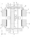
- FIG. 4 is a plan view showing an example of a substrate transport device
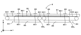
- FIGS. 5A and 5B are side views showing the substrate transport device of FIG. 4
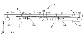
- FIGS. 6A, 6B, 7A, and 7B are front views showing the substrate transport device of FIG. 4
- FIGS. 8A and 8B are diagrams showing backup members used in the substrate transport device of FIG. 4.
- the board transport device 74 has a pair of conveyor units 8 spaced apart in the X direction, and a transport path Tb along which the board B passes in the Y direction is provided between the pair of conveyor units 8.
- the difference between the pair of conveyor units 8 is that one is provided at one end of the board B in the X direction, while the other is provided at the other end (opposite the one end) of the board B in the X direction, but they have a common configuration. Therefore, the explanation here will focus on one of the conveyor units 8.
- the conveyor unit 8 has a board guide 81 extending parallel to the Y direction along the transport path Tb.
- the board guide 81 has a side end face 811 at the end on the inside in the X direction (the transport path Tb side), and the side end face 811 is a vertical surface parallel to the Y direction and the Z direction.
- This side end face 811 is adjacent to the transport path Tb from the X direction, that is, it faces the end Be of the board B transported along the transport path Tb from the X direction.
- This board guide 81 is composed of the side end face 811 and a base part 812 that holds the side end face 811, and the side end face 811 and the base part 812 have different electrical characteristics, specifically, electrical resistance values.
- the side end face 811 is a static electricity diffusion surface that is composed of a conductive material other than metal (ceramics in this example) and has static electricity diffusion properties
- the base part 812 is metal and has a lower electrical resistance value than the side end face 811.
- a surface treatment process such as ceramic coating by thermal spraying or heat coating
- a thin layer that has static electricity diffusion properties can be formed on the base material of the base portion 812.
- the surface of this static electricity diffusion layer functions as the side end surface 811 (static diffusion surface).
- the conveyor unit 8 also has a belt conveyor 83 that is provided at the end of the transport path Tb in the X direction and supports the end of the substrate B located on the transport path Tb.
- the belt conveyor 83 has a plurality of pulleys 831 spaced apart in the Y direction and an endless belt 832 stretched around the pulleys 831.
- the upper surface of the endless belt 832 is a horizontal surface extending parallel to the Y direction.
- a plurality of (two) belt conveyors 83 are arranged in series in the Y direction, and the conveyor unit 8 transports the substrate B in the Y direction while transferring the substrate B between these belt conveyors 83. In this way, the substrate B transported in the Y direction by the belt conveyor 83 of the conveyor unit 8 passes through the transport path Tb.
- the endless belt 832 protrudes inward (towards the transport path Tb) from the side end surface 811 of the board guide 81, and the end Be of the board B is placed on the part of the endless belt 832 protruding from the side end surface 811. Therefore, the side end surface 811 of the board guide 81 faces the end Be of the board B placed on the endless belt 832 from the X direction. This side end surface 811 of the board guide 81 contacts the end Be of the board B displaced outward in the X direction (the opposite side of the transport path Tb), thereby guiding the board B along the transport path Tb.
- the conveyor unit 8 has a clamper 84 provided at the end of the transport path Tb in the X direction.
- the clamper 84 has an upper clamp member 85 that faces from above the upper surface Bu of the substrate B placed on the belt conveyor 83, and a lower clamp member 86 that faces from below the lower surface Bd of the substrate B placed on the belt conveyor 83.
- a plurality of upper clamp members 85 are arranged at intervals in the Y direction, and one lower clamp member 86 is provided corresponding to the plurality of upper clamp members 85.
- the upper clamp member 85 is attached to the upper surface of the board guide 81 and protrudes inward (toward the transport path Tb) from the side end surface 811 of the board guide 81 and the endless belt 832 in the X direction.
- the upper clamp member 85 is composed of a horizontal lower end surface 851 and a base portion 852 that holds the lower end surface 851, and the lower end surface 851 and the base portion 852 have different electrical characteristics, specifically, electrical resistance values.
- the lower end surface 851 is a static electricity diffusion surface that is composed of a conductive material other than metal (ceramics in this example) and has static electricity diffusion properties
- the base portion 852 is a metal that has a lower electrical resistance value than the lower end surface 851.
- the lower clamp member 86 is provided inward (on the transport path Tb side) from the side end surface 811 of the substrate guide 81 and the endless belt 832 in the X direction.
- the lower clamp member 86 is a plate that extends in the Y direction and is parallel to the Y and Z directions.
- the lower clamp member 86 is composed of an upper end surface 861 parallel to the Y direction and a base portion 862 that holds the upper end surface 861, and the upper end surface 861 and the base portion 862 have different electrical characteristics, specifically, electrical resistance values.
- a plurality (two) of lower clamp members 86 are arranged in the Y direction in correspondence with the plurality (two) of belt conveyors 83 arranged in the Y direction.
- a plurality (two) of upper clamp members 85 are provided for each of the two lower clamp members 86.
- the lower end surface 851 of the upper clamp member 85 and the upper end surface 861 of the lower clamp member 86 face each other in the Z direction, sandwiching the substrate B placed on the endless belt 832.
- the clamper 84 has a drive unit 87 that drives the lower clamp member 86 in the Z direction.
- the drive unit 87 is an actuator such as a solenoid or cylinder, and may be provided commonly to the multiple upper clamp members 85 or may be provided individually. This drive unit 87 drives the lower clamp member 86 in the Z direction between a lowered position 86L and an elevated position 86U that is above the lowered position 86L.
- the lower clamp member 86 which is located at the lowered position 86L, moves downward away from the substrate B supported by the belt conveyor 83.
- the drive unit 87 raises the lower clamp member 86 from the lowered position 86L, the upper end surface 861 of the lower clamp member 86 comes into contact with the lower surface of the substrate B, lifting the substrate B from the belt conveyor 83.
- the drive unit 87 lowers the lower clamp member 86 from the raised position 86U, the upper surface of the substrate B moves downward away from the lower end surface 851 of the upper clamp member 85, and the substrate B is transferred from the upper end surface 861 of the lower clamp member 86 to the belt conveyor 83. Furthermore, when the lower clamp member 86 moves downward to the lowered position 86L, the upper end surface 861 of the lower clamp member 86 moves downward away from the substrate B supported by the belt conveyor 83 (clamp release operation). As a result, the substrate B moves downward from the clamp position B2 to the belt placement position B1.
- the substrate transport device 74 includes a backup unit 9 disposed between a pair of conveyor units 8 in the X direction.
- the backup unit 9 includes a metal lift table 91 and a drive unit 92 that drives the lift table 91 in the Z direction.
- a plurality (two) of lift tables 91 are arranged in the Y direction in correspondence with a plurality (two) of belt conveyors 83 arranged in the Y direction.
- the drive unit 92 is, for example, an actuator such as a solenoid or cylinder, and may be provided commonly to the plurality of lift tables 91 or may be provided individually.
- the upper surface of the lift table 91 is a horizontal pin arrangement plane 911, and the backup unit 9 includes one or more backup members 93 arranged on the pin arrangement plane 911.
- the backup member 93 has a base plate 931, a metallic pin support 932 extending upward from the base plate 931, and a backup pin 94 attached to the pin support 932.
- the base plate 931 has a magnet, and when placed on the pin arrangement plane 911 of the lift table 91, it is attracted to the pin arrangement plane 911 by magnetic force.
- the pin support 932 has a plate fastening portion 933 fastened to the upper surface of the base plate 931, an erect portion 934 erected upward in the Z direction from the plate fastening portion 933, and a pin fastening portion 935 extending horizontally from the upper end of the erect portion 934, and the backup pin 94 is fastened to the pin fastening portion 935.
- the backup pin 94 has a metal shaft 95 erected from the pin fastening portion 935 upward in the Z direction, and a sphere 96 attached to the upper end of the shaft 95.
- the sphere 96 is composed of a sphere surface 961 and a base portion 962 that holds the sphere surface 961, and the sphere surface 961 and the base portion 962 have different electrical characteristics, specifically, electrical resistance values.
- the sphere surface 961 is an electrostatic diffusion surface that is composed of a conductive material (ceramics in this example) different from metal and has electrostatic diffusion properties
- the base portion 962 is a metal that has a lower electrical resistance value than the sphere surface 961.
- a thin layer (electrostatic diffusion layer) having electrostatic diffusion properties can be formed on the base material of the base portion 962 by performing a surface treatment process such as ceramic coating by thermal spraying or thermal coating on the surface of the metal that serves as the base material of the base portion 962.
- the surface of this electrostatic diffusion layer functions as the sphere surface 961 (electrostatic diffusion surface).
- the base material of the base portion 962 can be, for example, a ball used in a ball bearing.
- the backup pin 94 can be completed simply by pressing the ball into the shaft 95, and by using a ball having a sphere, there is no need to consider the orientation of the ball when pressing it, and the backup pin 94 can be easily assembled.
- the sphere 96 is fixed to the upper end of the shaft 95 and does not function as a bearing. In this way, the sphere 96 is provided at the tip of the backup pin 94, and the backup pin 94 supports the substrate B from below by the spherical surface 961 of the sphere 96.
- the backup pin 94 which is located at the lowered position 94L, moves downward away from the substrate B supported at the belt placement position B1 by the belt conveyor 83.
- the drive unit 92 raises the backup pin 94 from the lowered position 94L, the spherical surface 961 (upper end surface) of the backup pin 94 abuts against the underside of the substrate B at the belt placement position B1, lifting the substrate B from the belt conveyor 83. Then, as shown in FIGS.
- the spherical surface 961 of the backup pin 94 abuts against the underside of the substrate B clamped at the clamp position B2, supporting the substrate B from below (backup operation).
- This backup operation is performed simultaneously with the clamp operation described above.
- the backup position where the spherical surface 961 of the backup pin 94 abuts on the substrate B is on the inside (center) in the X direction relative to the clamp position (edge of substrate B) where the upper clamp member 85 and the lower clamp member 86 that clamp the substrate B abut on the substrate B.
- the drive unit 92 lowers the backup pin 94 from the raised position 94U, the substrate B is lowered and the substrate B is transferred from the spherical surface 961 of the backup pin 94 to the belt conveyor 83.
- the backup pin 94 is lowered to the lowered position 94L, the spherical surface 961 of the backup pin 94 moves downward away from the substrate B supported by the belt conveyor 83 at the belt placement position B1 (backup release operation). This backup release operation is performed simultaneously with the clamp release operation described above.
- the substrate B is transported along a predetermined transport path Tb.
- the substrate B located on the transport path Tb is supported or guided by the substrate contact surfaces (the side end surface 811 of the substrate guide 81, the lower end surface 851 of the upper clamp member 85, the upper end surface 861 of the lower clamp member 86, and the spherical surface 961 of the backup member 93) that contact the substrate B.
- the substrate contact surfaces 811, 851, 861, and 961 are conductive. Therefore, the electric charge accumulated on the substrate B flows out to the substrate contact surfaces 811, 851, 861, and 961 that contact the substrate B, and the electric charge on the substrate B is eliminated.
- the substrate contact surfaces 811, 851, 861, and 961 are not metal, the flow of electric charge from the substrate B to the substrate contact surfaces 811, 851, 861, and 961 is gently suppressed. In this way, it is possible to suppress the charging of the board B while slowing down the outflow of electric charge from the board B transported on the component mounting line 1.
- the electrical resistance of the board contact surfaces 811, 851, 861, and 961 can be set within a range that provides electrostatic dissipation. This makes it possible to suppress the charging of board B while easing the outflow of electric charge from board B being transported on component mounting line 1.
- the electrical resistance of the substrate contact surfaces 811, 851, 861, and 961 can be set to 1 ⁇ 10 ⁇ 4 ⁇ or more and less than 1 ⁇ 10 ⁇ 11 ⁇ .
- electrical resistance values in the range of 1 ⁇ 10 ⁇ 4 ⁇ or more and less than 1 ⁇ 10 ⁇ 11 ⁇ are indicated as electrical resistance values having electrostatic dissipation properties in IEC 61340-5-1 (standard).
- IEC 61340-5-1 standard
- the electrical resistance of the board contact surfaces 811, 851, 861, and 961 is 1 ⁇ 10 ⁇ 4 ⁇ or more, the outflow of electric charge from the board B to the board contact surfaces 811, 851, 861, and 961 is gently suppressed. In this way, it is possible to suppress the charging of the board B while easing the outflow of electric charge from the board B transported on the component mounting line 1.
- the substrate guide 81, the upper clamp member 85, the lower clamp member 86 and the sphere 96 have substrate parts (base parts 812, 852, 862 and 962) on which the substrate contact surfaces 811, 851, 861 and 961 are provided.
- the substrate guide 81, the upper clamp member 85, the lower clamp member 86 and the sphere 96 are not all made of ceramics, so that costs can be reduced.
- the hardness of the substrate contact surfaces 811, 851, 861 and 961 is higher than the hardness of the substrate parts 812, 852, 862 and 962. In this configuration, the durability of the substrate contact surfaces 811, 851, 861 and 961 can be increased, and deterioration of the substrate contact surfaces 811, 851, 861 and 961 due to contact with the substrate B can be suppressed.
- the substrate contact surfaces 811, 851, 861, and 961 are made of ceramics, which are highly resistant to friction and do not rust. This eliminates the need to replace the substrate contact surfaces 811, 851, 861, and 961 for a long period of time, reducing the burden of maintenance.
- the substrate contact surfaces 811, 851, 861, 961 may be made of coated ceramics as described above. By coating, the ceramics can be applied to form a very thin layer, and the substrate contact surfaces 811, 851, 861, 961 made of ceramics can be formed even for complex shapes.
- a board guide 81 is provided adjacent to the transport path Tb, and a side end surface 811 of the board guide 81 contacts the edge Be of the board B as a board contact surface having static electricity dissipation properties, i.e., a static electricity dissipation surface, to guide the board B.
- a board contact surface having static electricity dissipation properties i.e., a static electricity dissipation surface
- the side end surface 811 of the board guide 81 comes into contact with the board B frequently. Therefore, it is particularly preferable to configure the side end surface 811 of the board guide 81 as a board contact surface made of a material other than metal and having conductivity, i.e., a static electricity dissipation surface.
- a lower clamp member 86 that faces from below the substrate B supported by the belt conveyor 83 (substrate transport section), and an upper clamp member 85 that faces from above the substrate B supported by the belt conveyor 83.
- a clamping operation is performed in which the substrate B lifted from the belt conveyor 83 by the lower clamp member 86 is clamped between the lower clamp member 86 and the upper clamp member 85 by raising the lower clamp member 86 above the belt conveyor 83, and a clamp release operation is performed in which the clamping operation is released by lowering the lower clamp member 86 below the belt conveyor 83.
- an upper end surface 861 of the lower clamp member 86 contacts the lower surface of the substrate B as a substrate contact surface (static electricity diffusion surface), and a lower end surface 851 of the upper clamp member 85 contacts the upper surface of the substrate B as a substrate contact surface (static electricity diffusion surface). That is, the upper end surface 861 of the lower clamp member 86 and the lower end surface 851 of the upper clamp member 85 come into contact with the board B in order to clamp the board B.
- the upper surface (front surface) and the lower surface (back surface) of the board with which the upper end surface 861 of the lower clamp member 86 and the lower end surface 851 of the upper clamp member 85 come into contact correspond to the surface on which the component P is mounted (i.e., the surface on which the land is provided). Therefore, from the viewpoint of preventing damage to the component P, it is particularly preferable to configure the upper end surface 861 of the lower clamp member 86 and the lower end surface 851 of the upper clamp member 85 as a board contact surface (static electricity dissipation surface) made of a material other than metal and having conductivity.
- a backup pin 94 is provided that faces the board B supported by the belt conveyor 83 from below.
- a backup operation is performed in which the backup pin 94 is raised above the belt conveyor 83 to support the board B lifted from the belt conveyor 83 by the backup pin 94, and a backup release operation is performed in which the backup pin 94 is lowered below the belt conveyor 83 to release the backup operation.
- the spherical surface 961 (upper end surface) of the backup pin 94 contacts the lower surface of the board B as a board contact surface (static electricity diffusion surface). In other words, the spherical surface 961 of the backup pin 94 contacts the board B to support the board B.
- the backup pin 94 contacts the board B relatively close to the center of the board B, in other words, near the mounting position (i.e., the land) of the component P. Therefore, from the viewpoint of preventing damage to the component P, it is particularly preferable to configure the spherical surface 961 of the backup pin 94, which is a board contact surface (static electricity diffusion surface) made of a material other than metal and has conductivity.
- the component mounter 4 corresponds to an example of a "component mounter” of the present invention
- the head unit 43 corresponds to an example of a “mounting unit” of the present invention
- the board transport device 74 corresponds to an example of a "board transport device” of the present invention
- the belt conveyor 83 corresponds to an example of a "board transport section” of the present invention
- each of the side end surface 811, the lower end surface 851, the upper end surface 861 and the spherical surface 961 corresponds to an example of a "board contact surface” of the present invention
- the board guide 81, the clamper 84 and the backup unit 9 work together to form an example of a "board transport auxiliary section" of the present invention.
- base portion 812, base portion 852, base portion 862, and base portion 962 corresponds to an example of a "substrate portion" of the present invention
- board guide 81 corresponds to an example of a "board guide” of the present invention
- lower clamp member 86 corresponds to an example of a “lower clamp member” of the present invention
- upper clamp member 85 corresponds to an example of an “upper clamp member” of the present invention
- backup pin 94 corresponds to an example of a "backup pin” of the present invention
- board B corresponds to an example of a "board” of the present invention
- transport path Tb corresponds to an example of a "transport path” of the present invention.
- the substrate contact surfaces 811, 851, 861, 961 may be formed by anodizing.
- Anodizing allows the substrate contact surfaces 811, 851, 861, 961 to be formed even for complex shapes, and since anodizing is inexpensive, it is also possible to reduce the cost of the substrate transport device 74.
- the substrate contact surfaces 811, 851, 861, 961 may also be formed by DLC processing. DLC processing can form the substrate contact surfaces 811, 851, 861, 961 with high precision even for complex shapes. It can also form the substrate contact surfaces 811, 851, 861, 961 with high hardness and wear resistance. Furthermore, since the substrate contact surfaces 811, 851, 861, 961 can be formed with a low coefficient of friction, the substrate contact surfaces 811, 851, 861, 961 do not impede smooth transport of the substrate B.
- the number of belt conveyors 83 in the conveyor unit 8 is not limited to two, and may be one or three or more. Furthermore, when multiple belt conveyors 83 are provided, as in the above example, multiple belt conveyors 83 may support one board B, or each of the multiple belt conveyors 83 may support one board B.
- the shape of the substrate B is not limited to the rectangular shape described above, and may be any shape other than rectangular.
Landscapes
- Engineering & Computer Science (AREA)
- Manufacturing & Machinery (AREA)
- Microelectronics & Electronic Packaging (AREA)
- Supply And Installment Of Electrical Components (AREA)
Priority Applications (3)
| Application Number | Priority Date | Filing Date | Title |
|---|---|---|---|
| DE112022007819.7T DE112022007819T5 (de) | 2022-12-20 | 2022-12-20 | Leiterplattentransportvorrichtung, Bestückungsautomat und Leiterplattentransportverfahren |
| PCT/JP2022/046795 WO2024134748A1 (ja) | 2022-12-20 | 2022-12-20 | 基板搬送装置、部品実装機および基板搬送方法 |
| JP2024565427A JPWO2024134748A1 (https=) | 2022-12-20 | 2022-12-20 |
Applications Claiming Priority (1)
| Application Number | Priority Date | Filing Date | Title |
|---|---|---|---|
| PCT/JP2022/046795 WO2024134748A1 (ja) | 2022-12-20 | 2022-12-20 | 基板搬送装置、部品実装機および基板搬送方法 |
Publications (1)
| Publication Number | Publication Date |
|---|---|
| WO2024134748A1 true WO2024134748A1 (ja) | 2024-06-27 |
Family
ID=91588123
Family Applications (1)
| Application Number | Title | Priority Date | Filing Date |
|---|---|---|---|
| PCT/JP2022/046795 Ceased WO2024134748A1 (ja) | 2022-12-20 | 2022-12-20 | 基板搬送装置、部品実装機および基板搬送方法 |
Country Status (3)
| Country | Link |
|---|---|
| JP (1) | JPWO2024134748A1 (https=) |
| DE (1) | DE112022007819T5 (https=) |
| WO (1) | WO2024134748A1 (https=) |
Cited By (1)
| Publication number | Priority date | Publication date | Assignee | Title |
|---|---|---|---|---|
| WO2026069477A1 (ja) * | 2024-09-25 | 2026-04-02 | ヤマハ発動機株式会社 | バックアップピン配置支援装置、半田印刷機、バックアップピン配置支援方法、バックアップピン配置支援プログラムおよび記録媒体 |
Citations (8)
| Publication number | Priority date | Publication date | Assignee | Title |
|---|---|---|---|---|
| JPS6467999A (en) * | 1987-09-08 | 1989-03-14 | Sanyo Electric Co | Printed board positioning device |
| JPH10139091A (ja) * | 1996-11-11 | 1998-05-26 | Dainichi Shoji Kk | 基板用カセットにおけるサイドレール |
| JP2011091460A (ja) * | 2011-02-09 | 2011-05-06 | Fuji Mach Mfg Co Ltd | 基板保持装置 |
| JP2014232802A (ja) * | 2013-05-29 | 2014-12-11 | 京セラ株式会社 | 部品吸着装置およびそれに用いる吸着ノズル |
| JP2019140353A (ja) * | 2018-02-15 | 2019-08-22 | 京セラ株式会社 | バックアップピン、バックアップピン組み立て体および部品実装機 |
| WO2020152766A1 (ja) * | 2019-01-22 | 2020-07-30 | 株式会社Fuji | 搬送装置 |
| JP2021174879A (ja) * | 2020-04-24 | 2021-11-01 | ヤマハ発動機株式会社 | 基板作業システム、基板作業ライン用の電源スイッチおよび基板作業ラインの電源管理方法。 |
| JP2021180237A (ja) * | 2020-05-13 | 2021-11-18 | 株式会社Fuji | 部品実装機 |
-
2022
- 2022-12-20 WO PCT/JP2022/046795 patent/WO2024134748A1/ja not_active Ceased
- 2022-12-20 DE DE112022007819.7T patent/DE112022007819T5/de active Pending
- 2022-12-20 JP JP2024565427A patent/JPWO2024134748A1/ja active Pending
Patent Citations (8)
| Publication number | Priority date | Publication date | Assignee | Title |
|---|---|---|---|---|
| JPS6467999A (en) * | 1987-09-08 | 1989-03-14 | Sanyo Electric Co | Printed board positioning device |
| JPH10139091A (ja) * | 1996-11-11 | 1998-05-26 | Dainichi Shoji Kk | 基板用カセットにおけるサイドレール |
| JP2011091460A (ja) * | 2011-02-09 | 2011-05-06 | Fuji Mach Mfg Co Ltd | 基板保持装置 |
| JP2014232802A (ja) * | 2013-05-29 | 2014-12-11 | 京セラ株式会社 | 部品吸着装置およびそれに用いる吸着ノズル |
| JP2019140353A (ja) * | 2018-02-15 | 2019-08-22 | 京セラ株式会社 | バックアップピン、バックアップピン組み立て体および部品実装機 |
| WO2020152766A1 (ja) * | 2019-01-22 | 2020-07-30 | 株式会社Fuji | 搬送装置 |
| JP2021174879A (ja) * | 2020-04-24 | 2021-11-01 | ヤマハ発動機株式会社 | 基板作業システム、基板作業ライン用の電源スイッチおよび基板作業ラインの電源管理方法。 |
| JP2021180237A (ja) * | 2020-05-13 | 2021-11-18 | 株式会社Fuji | 部品実装機 |
Cited By (1)
| Publication number | Priority date | Publication date | Assignee | Title |
|---|---|---|---|---|
| WO2026069477A1 (ja) * | 2024-09-25 | 2026-04-02 | ヤマハ発動機株式会社 | バックアップピン配置支援装置、半田印刷機、バックアップピン配置支援方法、バックアップピン配置支援プログラムおよび記録媒体 |
Also Published As
| Publication number | Publication date |
|---|---|
| DE112022007819T5 (de) | 2025-07-10 |
| JPWO2024134748A1 (https=) | 2024-06-27 |
Similar Documents
| Publication | Publication Date | Title |
|---|---|---|
| JP3778159B2 (ja) | 印刷回路基板の移送装置 | |
| EP2185362B1 (en) | Workpiece processing system and method | |
| KR101470996B1 (ko) | 땜납 볼 인쇄 탑재 장치 | |
| KR102152009B1 (ko) | 볼 탑재 장치 | |
| KR101740493B1 (ko) | 납빠짐성이 개선된 스크린프린터와 이것의 제어방법 | |
| KR20000073365A (ko) | 표면실장기의 인쇄회로기판 평면도 보정장치 | |
| WO2024134748A1 (ja) | 基板搬送装置、部品実装機および基板搬送方法 | |
| JP4950831B2 (ja) | 基板搬送コンベヤ | |
| JP4995977B2 (ja) | 基板保持装置 | |
| KR101251562B1 (ko) | 칩 트레이 공급장치 | |
| JP7507395B2 (ja) | フィーダ及びキャリアテープの搬送方法 | |
| JP4494910B2 (ja) | 表面実装装置 | |
| JP4527131B2 (ja) | 実装機 | |
| CN219592982U (zh) | 多点贴合装置及贴合设备 | |
| JP4992871B2 (ja) | 電子部品実装システム | |
| KR101133124B1 (ko) | 부품실장기용 기판지지장치 | |
| JP2002299857A (ja) | 脆性材料製基板支持方法および回路基板支持装置ならびに電気回路製造方法 | |
| JP3101485U (ja) | プリント基板クリーニング装置 | |
| JP2016004964A (ja) | 基板搬送装置 | |
| JP3957157B2 (ja) | 実装機 | |
| JP2019021853A (ja) | 部品実装装置および部品実装方法ならびにペースト供給装置 | |
| JP7109076B2 (ja) | 基板吸着固定ステージ及びボール搭載装置 | |
| JP2000340995A (ja) | 基板支持装置 | |
| JPWO2020152735A1 (ja) | 搬送装置 | |
| JP2017195228A (ja) | 部品実装装置および部品実装装置用ヘッドユニット |
Legal Events
| Date | Code | Title | Description |
|---|---|---|---|
| 121 | Ep: the epo has been informed by wipo that ep was designated in this application |
Ref document number: 22969137 Country of ref document: EP Kind code of ref document: A1 |
|
| WWE | Wipo information: entry into national phase |
Ref document number: 2024565427 Country of ref document: JP |
|
| WWE | Wipo information: entry into national phase |
Ref document number: 112022007819 Country of ref document: DE |
|
| WWP | Wipo information: published in national office |
Ref document number: 112022007819 Country of ref document: DE |
|
| 122 | Ep: pct application non-entry in european phase |
Ref document number: 22969137 Country of ref document: EP Kind code of ref document: A1 |